JP2017116885A - LED display device - Google Patents
LED display device Download PDFInfo
- Publication number
- JP2017116885A JP2017116885A JP2015255374A JP2015255374A JP2017116885A JP 2017116885 A JP2017116885 A JP 2017116885A JP 2015255374 A JP2015255374 A JP 2015255374A JP 2015255374 A JP2015255374 A JP 2015255374A JP 2017116885 A JP2017116885 A JP 2017116885A
- Authority
- JP
- Japan
- Prior art keywords
- led
- substrate
- display device
- led element
- flexible transparent
- Prior art date
- Legal status (The legal status is an assumption and is not a legal conclusion. Google has not performed a legal analysis and makes no representation as to the accuracy of the status listed.)
- Pending
Links
Images


Landscapes
- Led Device Packages (AREA)
- Devices For Indicating Variable Information By Combining Individual Elements (AREA)
- Structure Of Printed Boards (AREA)
Abstract
Description
本発明は、LED表示装置に関する。詳しくは、フレキシブル透明基板を用いたカラー表示型のLED表示装置に関する。 The present invention relates to an LED display device. Specifically, the present invention relates to a color display type LED display device using a flexible transparent substrate.
平面又は曲面上に実装されたLED素子を選択的に発光させることにより、所望の文字、記号、又は図柄を構成して表示するドットマトリックス表示装置等、各種のLED表示装置の普及が進んでいる。例えば、電子部品を収納した筐体面に表示窓を形成し、複数のLED素子をマトリックス状に配線基板上に配列したLED表示パネルを設け、表示制御装置でこのLED表示パネルのLED素子を表示制御するように構成されているLED表示装置等が知られている(特許文献1参照)。 Various LED display devices such as a dot matrix display device that forms and displays a desired character, symbol, or pattern by selectively emitting LED elements mounted on a plane or a curved surface have been widely used. . For example, a display window is formed on the surface of a housing containing electronic components, an LED display panel in which a plurality of LED elements are arranged in a matrix on a wiring board is provided, and the display control device controls display of the LED elements of the LED display panel. An LED display device or the like configured to do this is known (see Patent Document 1).
このようなLED表示装置の一形態として、近年では、赤(R)、緑(G)、青(B)の高輝度発光が可能なLED素子を用いて混色発光させることによりフルカラーでの表示を行うことができるLED表示装置の普及も進んでいる(特許文献2及び3参照)。 As one form of such an LED display device, in recent years, full-color display can be performed by emitting mixed colors using LED elements capable of high-luminance emission of red (R), green (G), and blue (B). LED display devices that can be used are also spreading (see Patent Documents 2 and 3).
RGB方式によるフルカラー表示型のLED表示装置は、RGB3原色の発光が可能なLED素子を単位画素としてフルカラーで絵や文字等の情報を表示する。このようなフルカラー表示型のLED表示装置は、例えば、特許文献2に開示されているように、3色の発光チップを1パッケージの素子内に一体化した所謂3in1タイプのマルチチップLED素子を単位画素として、これらを配線基板上にマトリクス状に実装することによって構成することができる。 A full color display type LED display device using the RGB method displays information such as pictures and characters in full color using LED elements capable of emitting light of RGB three primary colors as unit pixels. Such a full-color display type LED display device is, for example, a so-called 3 in 1 type multi-chip LED element in which three color light emitting chips are integrated in one package element as disclosed in Patent Document 2. The pixels can be configured by mounting them in a matrix on a wiring board.
しかしながら、3in1タイプのマルチチップLED素子は、一般に素子の単価が高額で、又、各単色のチップの輝度にも制約がある場合が多く、往々にして十分に高い輝度を得ることができない。特に屋外に設置する大型の表示装置等、大きな輝度が求められる場合に、十分に輝度の高いLED素子を選択できない場合が多い。この場合には、赤色(R)、緑色(G)、青色(B)のそれぞれの単色発光のLED素子各1つずつ、計3つを1組として、配線基板上に近接して配置することにより、RGB方式によるフルカラー表示のための単位画素を構成することもできる(特許文献3参照)。 However, the 3-in-1 type multi-chip LED element generally has a high unit price, and there are many cases where the luminance of each single-color chip is also limited, so that a sufficiently high luminance cannot often be obtained. In particular, when large luminance is required, such as a large display device installed outdoors, it is often impossible to select an LED element with sufficiently high luminance. In this case, each LED element for single-color emission of red (R), green (G), and blue (B) is arranged in a close proximity on the wiring board, a total of three. Thus, a unit pixel for full color display by the RGB method can be configured (see Patent Document 3).
ただし、R、G、Bのそれぞれの単色発光のLED素子を、汎用的な配線基板であるリジット基板等に実装するためには極めて複雑な回路形成が余儀なくされ、又、製造の難易度とコストも著しく上昇する。又、同一平面状においてこれらの複数のLED素子を近接配置することについては、各LED素子の全体形状やサイズに起因する物理的制約により、発光原である各LED素子内の発光チップ間の距離を十分に小さくできない場合がある。各LED素子内の発光チップ間の距離を十分に小さくできないと、RGB混色によるフルカラー表示に係る色品位を十分に向上させることができないという問題が生じる。 However, in order to mount each R, G, B single color light emitting LED element on a rigid substrate, which is a general-purpose wiring substrate, it is necessary to form an extremely complicated circuit, and the difficulty and cost of manufacturing. Also rises significantly. In addition, regarding the close placement of these LED elements in the same plane, the distance between the light emitting chips in each LED element that is the light source is due to physical restrictions due to the overall shape and size of each LED element. May not be sufficiently small. If the distance between the light emitting chips in each LED element cannot be made sufficiently small, there arises a problem that the color quality relating to full color display by RGB color mixing cannot be sufficiently improved.
本発明は、以上のような状況に鑑みてなされたものであり、例えばRGB方式のフルカラー表示タイプのLED表示装置等、カラー表示が可能なLED表示装置であって、高輝度且つ高品位の表示が可能でありながら、経済性にも優れるLED表示装置を提供することを目的とする。 The present invention has been made in view of the above situation, and is an LED display device capable of color display, such as a RGB full-color display type LED display device, for example, having high luminance and high quality display. An object of the present invention is to provide an LED display device that is excellent in economic efficiency.
本発明者らは、鋭意研究を重ねた結果、カラー表示型のLED表示装置において、発光色の異なる複数種類且つ複数のLED素子を実装する配線基板を、複数のフレキシブル透明基板を積層してなる多層LED素子基板とし、複数種類のLED素子を、発光色毎に各フレキシブル透明基板からなる層に、垂直分離配置することにより、上記課題を解決できることを見出すに至った。具体的に本発明は以下のものを提供する。 As a result of intensive research, the present inventors have laminated a plurality of flexible transparent substrates on a wiring board on which a plurality of types and a plurality of LED elements having different emission colors are mounted in a color display type LED display device. The present inventors have found that the above-described problems can be solved by arranging a plurality of types of LED elements in a layer composed of each flexible transparent substrate for each emission color, as a multilayer LED element substrate. Specifically, the present invention provides the following.
(1) 発光色が異なる複数のLED素子の組合せによって、多色表示可能な単位画素を構成し、該単位画素を、複数配置することにより、多色表示を行うLED表示装置であって、LED素子を実装する回路基板が、前記単位画素を構成するLED素子の色の種類数と同数以上の枚数のフレキシブル透明基板が積層されてなる多層LED素子基板であり、前記フレキシブル透明基板の表面には、各前記フレキシブル透明基板毎にそれぞれ異なる、同一発光色のLED素子が実装されており、発光色が異なる複数の前記LED素子が、前記多層LED素子基板の平面視上において、相互に近接して配置されていることによって、多色表示可能な前記単位画素を構成しているLED表示装置。 (1) An LED display device that performs multicolor display by configuring a unit pixel capable of multicolor display by combining a plurality of LED elements having different emission colors, and arranging a plurality of the unit pixels. The circuit board on which the element is mounted is a multilayer LED element substrate in which a number of flexible transparent substrates equal to or more than the number of types of colors of the LED elements constituting the unit pixel are laminated, and on the surface of the flexible transparent substrate The LED elements having the same emission color are mounted on the respective flexible transparent substrates, and the plurality of LED elements having different emission colors are close to each other in a plan view of the multilayer LED element substrate. An LED display device constituting the unit pixel capable of multicolor display by being arranged.
(1)の発明は、従来、当然に回路基板の同一面上に配置されていた一の単位画素を構成する複数のLED素子を、発光色別に多層LED素子基板を構成する各フレキシブル透明基板層にふり分けて、即ち、垂直方向に分離配置して、これとともに、多層LED素子基板の平面視上、即ち、水平方向においては、発光色の混色が可能な程度に近接配置することにより、RGB混色によるフルカラー発光が可能な単位画素を構成した。これにより、3in1タイプの素子を用いる場合に問題となっていた輝度不足の制約から逃れ、又、回路基板の同一面上に全ての必要な回路を形成する場合よりも、各層毎の回路構成は格段にシンプルな構成とすることができる。以上より、複数色の混色によりカラー表示が可能なLED表示装置について、生産コストの上昇を抑制しながら、表示色の品位を十分に向上させることができる。尚、「発光色が異なる」とは、例えば、分光分布のピーク波長が異なることを言うものとする。 According to the invention of (1), a plurality of LED elements constituting one unit pixel, which is naturally arranged on the same surface of a circuit board, are each flexible transparent substrate layer constituting a multilayer LED element substrate for each emission color. In other words, by arranging them separately in the vertical direction, and arranging them in close proximity to each other in a plan view of the multilayer LED element substrate, that is, in the horizontal direction, as close as possible to color mixing of the luminescent colors. A unit pixel capable of full color light emission by color mixing was constructed. This avoids the limitation of insufficient brightness that has been a problem when using 3 in 1 type elements, and the circuit configuration for each layer is less than when all necessary circuits are formed on the same surface of the circuit board. A much simpler configuration can be achieved. As described above, the quality of the display color can be sufficiently improved while suppressing an increase in production cost for the LED display device capable of performing color display by mixing a plurality of colors. Note that “the emission colors are different” means, for example, that the peak wavelengths of the spectral distribution are different.
(2) 前記単位画素を構成するLED素子の組合せが、RGB3原色を含む3種の色の組合せであって、前記多層LED素子基板が3層構造を有する多層基板であって、RGB3原色混光によるフルカラー表示が可能な(1)に記載のLED表示装置。 (2) The combination of the LED elements constituting the unit pixel is a combination of three kinds of colors including RGB three primary colors, and the multilayer LED element substrate is a multilayer substrate having a three-layer structure, and the RGB three primary color mixed light The LED display device according to (1), which is capable of full color display.
(2)の発明は、(1)のLED表示装置であって、RGB3原色混光によるフルカラー表示が可能なLED表示装置である。多層LED素子基板の各層を構成する材料基板を薄くて透明なフレキシブル透明基板とすることにより、RGBそれぞれのLED素子群の上記の垂直方向への適切な分離配置を容易に行うことが可能となっている。これにより、表示色の品位を保持したまま、従来よりも経済的にRGB方式によるフルカラー表示が可能なLED表示装置を得ることができる。 The invention of (2) is the LED display device of (1), which is capable of full-color display by RGB three primary color mixed light. By making the material substrate constituting each layer of the multilayer LED element substrate a thin and transparent flexible transparent substrate, it becomes possible to easily perform appropriate separation and arrangement in the vertical direction of each LED element group of RGB. ing. Thereby, it is possible to obtain an LED display device capable of full-color display by the RGB method more economically than in the past while maintaining the display color quality.
(3) 前記フレキシブル透明基板は、波長360nm以上830nm以下の光線透過率が80%以上である透明樹脂基板と、前記透明樹脂基板の表面に形成される金属配線部と、を含んで構成されている(1)又は(2)に記載のLED表示装置。 (3) The flexible transparent substrate includes a transparent resin substrate having a light transmittance of not less than 80% and a wavelength of not less than 360 nm and not more than 830 nm, and a metal wiring portion formed on the surface of the transparent resin substrate. The LED display device according to (1) or (2).
(3)の発明は、LED素子用のフレキシブル透明基板において、支持基板を可視光域における光線透過率が80%以上の極めて優れた透光性を有する樹脂基板で構成としたものである。これにより、表示色の品位のバラツキを極めて小さくすることができ、更に高品位での表示が可能なフルカラー表示型のLED表示装置を得ることができる。尚、上記波長域の光線透過率、即ち、可視光線透過率は、JIS R3212に準拠する方法により測定することができる。 According to the invention (3), in the flexible transparent substrate for LED elements, the support substrate is composed of a resin substrate having extremely excellent translucency with a light transmittance of 80% or more in the visible light region. As a result, the variation in display color quality can be made extremely small, and a full-color display type LED display device capable of displaying with higher quality can be obtained. In addition, the light transmittance of the said wavelength range, ie, visible light transmittance, can be measured by the method based on JISR3212.
(4) 前記フレキシブル透明基板は、ヘーズ値が8%以下である透明樹脂基板と、前記透明樹脂基板の表面に形成される金属配線部と、を含んで構成されている(1)又は(2)に記載のLED表示装置。 (4) The flexible transparent substrate includes a transparent resin substrate having a haze value of 8% or less and a metal wiring portion formed on the surface of the transparent resin substrate (1) or (2 LED display device described in).
(4)の発明は、LED素子用のフレキシブル透明基板において、支持基板をヘーズ値が8%以下の極めて優れた透光性を有する樹脂基板で構成としたものである。これにより、単位画素の色彩設計がより容易且つ厳密にできるようになり、更に高品位での表示が可能なフルカラー表示型のLED表示装置を得ることができる。尚、本明細書における「ヘーズ値」とは、JISK7136に準じた透明性試験によって測定したヘーズ値(%)のことを言うものとする。 Invention of (4) WHEREIN: In the flexible transparent substrate for LED elements, a support substrate is comprised with the resin substrate which has the very outstanding translucency whose haze value is 8% or less. As a result, the color design of the unit pixel can be made more easily and strictly, and a full color display type LED display device capable of displaying with higher quality can be obtained. The “haze value” in this specification refers to a haze value (%) measured by a transparency test according to JISK7136.
(5) 前記金属配線部は銅箔である(3)又は(4)に記載のLED表示装置。 (5) The LED display device according to (3) or (4), wherein the metal wiring portion is a copper foil.
(5)の発明は、(3)又は(4)の発明におけるフレキシブル透明基板の金属配線部を電気抵抗が極めて小さく、熱伝導性が高い銅箔で形成したものである。よって、金属配線部の基板表面の被覆率に対する相対的な電気供給安定性と放熱性は極めて高い水準となる。これにより、様々な製造条件、使用条件に係る所望の回路設計の下で、電気供給安定性と放熱性を好ましい範囲に保持することができる。 In the invention of (5), the metal wiring part of the flexible transparent substrate in the invention of (3) or (4) is formed of a copper foil having an extremely small electric resistance and high thermal conductivity. Therefore, relative power supply stability and heat dissipation with respect to the coverage of the substrate surface of the metal wiring portion are extremely high. Thereby, it is possible to maintain the electric supply stability and the heat dissipation within a preferable range under a desired circuit design according to various manufacturing conditions and use conditions.
(6) 前記フレキシブル透明基板上における前記金属配線部による表面被覆率が、いずれも2%以上10%以下であることにより、前記多層LED素子基板の基板開口率が、80%以上である(1)から(5)のいずれかに記載のLED表示装置。 (6) When the surface coverage by the metal wiring part on the flexible transparent substrate is 2% or more and 10% or less, the substrate aperture ratio of the multilayer LED element substrate is 80% or more (1 The LED display device according to any one of (5) to (5).
(6)の発明は、(1)から(5)のいずれかに記載のフレキシブル透明基板において、金属配線部による支持基板の表面被覆率を10%以下とした。フレキシブル透明基板において、十分な透光性を有する部分の割合である基板開口率が概ね80%以上となることによって、例えば、図6に示すような、表示画面の背面側に配置される視覚情報の視認性が高いシースルー型のLED表示装置とすることができる。 According to the invention (6), in the flexible transparent substrate according to any one of (1) to (5), the surface coverage of the support substrate by the metal wiring portion is set to 10% or less. Visual information arranged on the back side of the display screen as shown in FIG. 6, for example, as shown in FIG. The see-through type LED display device with high visibility can be obtained.
(7) 前記フレキシブル透明基板上の前記金属配線部による表面被覆率が、いずれも80%以上95%以下である(1)から(5)のいずれかに記載のLED表示装置。 (7) The LED display device according to any one of (1) to (5), wherein the surface coverage by the metal wiring portion on the flexible transparent substrate is 80% or more and 95% or less.
(7)の発明は、(1)から(5)のいずれかに記載のフレキシブル透明基板において、金属配線部による支持基板の表面被覆率を80%以上とした。LED素子において発生する熱の放出経路となる金属配線部の表面被覆率が高いことによって、放熱性と低電気抵抗性に優れた基板となる。これにより、それぞれのLED素子の消費電力が小さく、且つ、発光輝度のバラツキも抑えることができる。又、熱による基板等の周辺部材の劣化も防止して製品寿命を延長することができる。 In the invention of (7), in the flexible transparent substrate according to any one of (1) to (5), the surface coverage of the support substrate by the metal wiring portion is set to 80% or more. Since the surface coverage of the metal wiring portion serving as a path for releasing heat generated in the LED element is high, the substrate has excellent heat dissipation and low electrical resistance. Thereby, the power consumption of each LED element is small, and the variation in light emission luminance can also be suppressed. Further, deterioration of peripheral members such as a substrate due to heat can be prevented and the product life can be extended.
(8) 前記LED素子が表面実装用のチップ型LED素子であって、前記多層LED素子基板の平面視上において相互に近接して配置されて前記単位画素を構成している前記LED素子の発光チップ同士が、該平面視上においては重ならない位置に配置されていて、尚且つ、該LED素子の発光チップ以外の部分の一部が、該平面視上において相互に重なる位置に配置されている(1)から(7)のいずれかに記載のLED表示装置。 (8) The LED element is a chip-type LED element for surface mounting, and light emission of the LED element which is arranged close to each other in a plan view of the multilayer LED element substrate and constitutes the unit pixel The chips are arranged at positions where they do not overlap in the plan view, and parts of the LED elements other than the light emitting chips are arranged at positions where they overlap each other in the plan view. The LED display device according to any one of (1) to (7).
(8)の発明は、表面実装用のチップ型LED素子を基板の同一面上に近接して実装する場合のLED素子の全体形状やサイズによる制約(図5(a)参照)から逃れて、単位画素内における発光チップ間の水平方向における距離を、上記の制約による限界よりも更に縮小したものである。これにより、更に、混色によるフルカラー表示の品位を向上させることができる。 The invention of (8) escapes from restrictions due to the overall shape and size of the LED element when the surface-mounted chip type LED element is mounted close to the same surface of the substrate (see FIG. 5A), The distance in the horizontal direction between the light emitting chips in the unit pixel is further reduced from the limit due to the above-mentioned restrictions. Thereby, the quality of full color display by color mixture can be further improved.
(9) 前記多層LED素子基板の厚さが10mm以下である(1)から(8)のいずれかに記載のLED表示装置。 (9) The LED display device according to any one of (1) to (8), wherein the multilayer LED element substrate has a thickness of 10 mm or less.
(8)の発明によれば、(1)から(8)のいずれかに記載のLED表示装置を、基板材料として、フレキシブル基板を採用することによるメリットを享受して、極めて薄型の表示装置としたものである。LED素子の配置位置の垂直方向のずれのデメリットを最小化することができる。又、薄型化、軽量化によって、設置条件の自由度が著しく拡大する。 According to the invention of (8), the LED display device according to any one of (1) to (8) can enjoy the advantages of adopting a flexible substrate as a substrate material, It is a thing. The demerit of the vertical deviation of the arrangement position of the LED elements can be minimized. In addition, the degree of freedom in installation conditions is significantly increased by reducing the thickness and weight.
本発明によれば、多色表示が可能なLED表示装置であって、高輝度で高い色品位の表示が可能でありながら、経済性に優れるLED表示装置を提供することができる。 ADVANTAGE OF THE INVENTION According to this invention, it is an LED display apparatus which can display multicolor, Comprising: While being able to display high brightness and high color quality, the LED display apparatus excellent in economical efficiency can be provided.
以下、本発明のLED表示装置及び同LED表示装置に用いる多層LED素子基板について順次説明する。本発明は、以下の実施形態に何ら限定されず、本発明の目的の範囲内において、適宜変更を加えて実施することができる。 Hereinafter, the LED display device of the present invention and the multilayer LED element substrate used in the LED display device will be sequentially described. The present invention is not limited to the following embodiments, and can be implemented with appropriate modifications within the scope of the object of the present invention.
<LED表示装置>
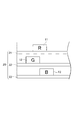
本発明のLED表示装置は、任意の多色、好ましくはフルカラーで発光可能な表示単位である複数の単位画素が、多層LED素子基板に実装されてなるカラー表示装置である。LED表示装置は、上記の単位画素の発光を制御することにより、所望の文字又は映像をカラー表示することができる。特に図1に示す、本発明に係るLED表示装置1は、単位画素10がRGBの3色のLED素子11、12、13で構成されていることにより、フルカラーでの表示が可能な表示装置である。
<LED display device>
The LED display device of the present invention is a color display device in which a plurality of unit pixels, which are display units capable of emitting light in any multicolor, preferably full color, are mounted on a multilayer LED element substrate. The LED display device can display a desired character or image in color by controlling the light emission of the unit pixel. In particular, the LED display device 1 according to the present invention shown in FIG. 1 is a display device capable of full-color display because the
本発明のLED表示装置は、図6に示すように、LED素子を実装する基板の透明性を生かして、シースルータイプのLED表示装置1Aとして実施することもできる。シースルータイプのLED表示装置1Aは、例えば図6に示すように、ショーウインドー等の前面に配置して用いられる実施形態が想定される。この場合、LED表示装置1Aの前面側に位置する者が、LED表示装置1Aに表示される情報の認知と同時並行的に、LED表示装置1Aの背面側にある視覚情報を視認することができる。
As shown in FIG. 6, the LED display device of the present invention can also be implemented as a see-through type
本発明のLED表示装置を、シースルータイプのLED表示装置1Aとして用いる場合には、後に詳述する通り、同LED表示装置を構成する多層LED素子基板の各層を構成するフレキシブル透明基板は、その金属配線部による表面被覆率が、いずれも2%以上10%以下であることが好ましい。金属配線部による表面被覆率が、いずれも2%以上10%以下であることにより、多層LED素子基板の基板開口率を、80%以上95%以下として、十分なシースルー機能をLED表示装置に備えさせることができる。尚、「多層LED素子基板の基板開口率」とは、多層LED素子基板の基板開口率の表面のうち、平面視上、金属配線部が存在しない部分の面積比率として定義される比率のことを言うものとする。
When the LED display device of the present invention is used as a see-through type
[単位画素]
単位画素10は、近接配置される複数の単色発光のLED素子の組合せによって構成される。1つの単位画素10を構成する複数のLED素子の具体的な個数は特定の個数に限定されない。例えば、赤(R)色のLED素子11、緑(G)色のLED素子12、及び青(B)色のLED素子13との、3個のLED素子の組合せにより、RGB方式によるフルカラーでの発光が可能な単位画素10を構成する例を好ましい例として挙げることができる。以下、単位画素10がRGBの3個のLED素子を組合せて1つの単位画素10を構成するLED表示装置1を、本発明の好ましい実施形態の一例として、その詳細を説明する。
[Unit pixel]
The
(LED素子)
LED表示装置1においては、LED素子として、表面実装用のチップ型LED素子を好ましく用いることができる。チップ型LED素子とは、回路上に直接実装するための電極(アノード及びカソード)や反射板等を一体化した樹脂製等の微細な梱包体に、P型半導体とN型半導体が接合されてなる発光体であるダイオード型の発光チップを内蔵した素子である。このチップ型LED素子を、発光色毎に、多層LED素子基板20を構成するフレキシブル透明基板21、22、23の所定位置に実装することにより単位画素10を構成することができる。
(LED element)
In the LED display device 1, a chip-type LED element for surface mounting can be preferably used as the LED element. A chip-type LED element is a P-type semiconductor and an N-type semiconductor bonded to a fine packing made of resin, etc., in which electrodes (anode and cathode) and a reflector for mounting directly on a circuit are integrated. It is an element having a built-in diode-type light-emitting chip as a light emitter. The
LED素子11、12、13としては、赤色発光する発光チップ111を内蔵した赤色のLED素子11と、緑発光する発光チップ121を内蔵した緑色のLED素子12と、青色発光する発光チップ131を内蔵した青色のLED素子13(以上図4及び図5参照)との組合せが好ましく用いられる。これら各色のLED素子11、12、13は、各色1個ずつ計3個の組合せによって、1つの単位画素10を形成することができるように、一定の配列パターンに基づいて、多層LED素子基板20に実装される。
The
[多層LED素子基板]
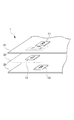
図2及び図3に示す通り、LED表示装置1においては、LED素子11、12、13を実装するための回路基板として、多層LED素子基板20が用いられる。多層LED素子基板20は、実装されるLED素子の発光色の種類数(本実施形態では3種類)と同数以上の枚数のフレキシブル透明基板(21、22、23)が積層されてなる多層構成の回路基板である。図2及び3においては、LED素子がR、G、Bの3色3種類のLED素子11、12、13からなり、3枚のフレキシブル透明基板21、22、23が積層されてなる多層LED素子基板20が用いられている。そして、フレキシブル透明基板21、22、23からなる各層に、これらのLED素子11、12、13がそれぞれ分離配置されている。
[Multilayer LED element substrate]
As shown in FIGS. 2 and 3, in the LED display device 1, a multilayer
多層LED素子基板20のサイズについては、特段の限定はない。但し、基板材料としてフレキシブル基板を用いていることより、基板のサイズ加工の自由度が高いため、特に屋外での使用を前提とした大型のLED表示装置に好ましく用いることができる。例えば、対角線の長さが32インチ以上、より好ましくは65インチ以上の大型の表示画面を備えるLED表示装置においても、多層LED素子基板20を回路基板として好ましく用いることができる。
There is no special limitation on the size of the multilayer
図2及び図3に示す通り、1つの単位画素10を構成するために近接配置される複数のそれぞれ異なる光を発光するLED素子11、12、13は、各色のLED素子毎に、多層LED素子基板20を構成するフレキシブル透明基板21、22、23の表面に実装されている。例えば、表示面側から順にフレキシブル透明基板21、22、23がこの順で積層されている図2及び図3の例においては、赤色のLED素子11を、全てフレキシブル透明基板21上に、緑色のLED素子12が、全てフレキシブル透明基板22上に、そして、青色のLED素子13が、全てフレキシブル透明基板23上に配置されている。このようなLED素子11、12、13の配置により、高品位でフルカラーの発光が可能な単位画素10を構成することができる。尚、RGBの各素子の垂直方向における配置の順序は、必ずしもこの順序に限られない。
As shown in FIG. 2 and FIG. 3, a plurality of
3層の各フレキシブル透明基板21、22、23に分離配置される、発光色の異なる各LED素子間の垂直方向における配置位置の差異は、実装されるLED素子の発光性能、例えば輝度や発光の指向性にもよって異なるが、概ね、各LED素子(例えば、図2におけるLED素子11と12)の、それぞれの発光面側の表面の垂直位置の差異が10mm以内であることが好ましい。例えば、各LED素子の厚さが1mm以上3mm以下程度であれば、各フレキシブル透明基板21、22、23の厚さを、50μm以上200μm以下の範囲とすることで、上記の通り、LED素子間の垂直方向における配置位置の差異を10mm程度とすることができる。従来の汎用的なリジット基板では、この厚さの基板を形成することは実質的に不可能であるが、基板材料をフレキシブル基板とすることにより、上記厚さ範囲にある多層LED素子基板を容易に形成することができる。
The difference in the arrangement position in the vertical direction between the LED elements having different emission colors that are separately arranged on the three layers of the flexible
複数種類のLED素子は、垂直方向においては、上記の通り発光色毎に多層LED素子基板20の内部において垂直方向に分配されるが、図1及び図3に示す通り、多層LED素子基板20の水平方向においては、一組のLED素子11、12、13が、1つの単位画素10を構成してフルカラーの表示機能を発現可能な程度に、平面視上において相互に十分に近接するように配置される。1つの単位画素10を構成するLED素子間の平面視上における距離については、チップ型LED素子を用いる場合においては、上記の通り、LED素子の垂直位置の差異が10mm以内であることを前提とした場合には、平面視上における、発光チップ(例えば、図2における発光チップ111と121)の各中心間の距離が、概ね10mm以内であることが好ましい。
In the vertical direction, the plurality of types of LED elements are distributed in the vertical direction inside the multilayer
図5に示す通り、LED素子が、チップ型LED素子である場合、1つの単位画素10を構成する各LED素子11、12、13は、多層LED素子基板20の平面視上において各LED素子の発光チップ111、121、131同士が、いずれも、それぞれ、上記平面視上において重ならない位置に配置することが必要である。更に、従来品においては、図5(a)に示す通り、各LED素子11、12、13の発光チップ以外の部分、具体的には上述した電極(アノード及びカソード)や反射板等を一体化した梱包体の外縁が、LED素子同士で相互に干渉しない位置にまで各LED素子を引き離して配置する必要があった。しかし、LED表示装置1においては、図5(b)に示す通り、各LED素子の発光チップ以外の部分の一部を、上記平面視上において相互に重なる位置に配置することもできる(単位画素10A)。これにより、この重なり部分の分だけ、従来品よりも、各LED素子の発光チップ同士の距離を短くして、単位画素毎のカラー発光の色品位を更に向上させることができる。又、それぞれの単位画素10の外縁が縮小されることにより、画素10の間のピッチを縮小して、表示画面単位面積当りの画素数を増やして、表示品位を向上させることもできる。
As shown in FIG. 5, when the LED element is a chip-type LED element, the
又、図4に示す通り、多層LED素子基板20において、各LED素子を実装するための金属配線部30(31、32、33)は、各LED素子11、12、13がそれぞれ積層されるフレキシブル透明基板21、22、23の各表面に形成される。図4に示すように、例えば、最下層側に配置される青色のLED素子13が実装される金属配線部33については、平面視において他の色のLED素子の発光チップと垂直方向に置いて重なっていたとしても、その他のLED素子からの発光の障害とはならない。ところが、例えば、緑色のLED素子12が実装される金属配線部32については図4に示す通り、それよりも下層に配置されるLED素子13の発光チップ131と、平面視において重なる位置を回避させて形成させる。
In addition, as shown in FIG. 4, in the multilayer
多層LED素子基板20は、複数のフレキシブル透明基板を、LED素子11、12、13が実装された状態で、重ね合わせる方法や或いは積層することによって積層一体化し製造することができる。
The multilayer
(フレキシブル透明基板)
多層LED素子基板20の各層を形成するフレキシブル透明基板21、22、23としては、透明性を有する樹脂基板の表面に金属配線部30が形成されているものであれば、従来公知のフレキシブル基板を適宜用いることができる。又、通常、フレキシブル透明基板21、22、23は、絶縁保護膜(図視せず)が、支持基板及び金属配線部30上におけるLED素子11、12、13の実装領域を除く領域を覆って積層されている。
(Flexible transparent substrate)
As the flexible
フレキシブル透明基板21、22、23は、「透明性」を有する回路基板であることが必要である。但し、必ずしもその全体が透明であることを必須とはしない。少なくとも、単位画素10から発光される光を、外部から視認するために必要な範囲が「透明」であればよい。本明細書においては、フレキシブル基板において、「透明性を有する」とは、当該部分の可視光域(波長360nm以上830nm以下)の光線透過率が80%以上、好ましくは、90%以上であることを言うものとする。上記光線透過率が80%以上であれば、表示色の品位のバラツキを極めて小さくすることができ、更に高品位での表示が可能なフルカラー表示型のLED表示装置を得ることができる。更に同光線透過率が90%以上であれば、より高品位、傾向としては、よりハイコントラストでよりシャープな映像の表示が可能となる。
The flexible
又、フレキシブル基板の透明性の他の指標として、上記同様の部分における、ヘーズ値が8%以下であることが好ましく、4%以下であることがより好ましい。ヘーズ値が8%以下であれば、下層側に配置される各単位画素からの様々な発光色を、異なる色として認識可能である。更にヘーズ値が4%以下であれば、RGB方式によるフルカラーの表示品位を見かけ上、ほぼ減衰させることなく視認者に認識させることができる。 Further, as another index of the transparency of the flexible substrate, the haze value in the same part as described above is preferably 8% or less, more preferably 4% or less. If the haze value is 8% or less, various emission colors from each unit pixel arranged on the lower layer side can be recognized as different colors. Further, if the haze value is 4% or less, it is possible to make the viewer recognize the display without any substantial attenuation in terms of the full color display quality by the RGB method.
透明性、耐熱性、絶縁性等が求められるフレキシブル透明基板21、22、23の支持基板として用いる樹脂の好ましい例として、ポリイミド(PI)、ポリエチレンナフタレート(PEN)、ポリエチレンテレフタレート(PET)、非晶ポリアリレート、ポリサルフォン、ポリエーテルサルフォン、ポリエーテルイミド、フッ素樹脂、液晶ポリマー等を挙げることができる。中でも、アニール処理等の耐熱性向上処理を施すことによって耐熱性と寸法安定性を向上させたポリエチレンナフタレート(PEN)を特に好ましく用いることができる。
Preferred examples of the resin used as the support substrate for the flexible
フレキシブル透明基板21、22、23の支持基板の厚さは、特に限定されないが、多層LED素子基板20として積層された際におけるLED素子の垂直方向への分離配置を上述の垂直位置の差異の範囲に保持する観点から、概ね50μm以上200μm以下程度であることが好ましい。又、ロール・トゥ・ロール方式による製造を行う場合の生産性を良好に維持する観点からも上記厚さ範囲であることが好ましい。
The thickness of the support substrate of the flexible
フレキシブル透明基板21、22、23の表面には、金属箔等の導電性基材によって金属配線部30が形成される。金属配線部30は、LED素子間を導通して必要な電流を流して電気を供給する機能を有するとともに、フレキシブル透明基板21、22、23における放熱部としての作用をも発揮する。
On the surface of the flexible
尚、フレキシブル透明基板のシースルー機能を最大化するために、金属配線部を透明電極で形成することも考えられる。しかしながら、透明電極は、LED素子用基板の全面に配置される回路全体に安定的に均一な電圧を正確にかける上での信頼性や、製造コストの面で、従来、広く用いられている銅箔等の金属配線に劣る。又、基板からの放熱を促進するために金属配線は熱伝導性が高いものであることが好ましいが、この点においても、銅箔等が明らかに優位である。この金属箔優位の傾向は、特に、表示面の画面サイズが大型になるほど顕著となる。よって、本発明のLED表示装置1においては、シースルータイプのもととして用いる場合であっても、金属配線部は銅等の熱伝導率の高い金属であることがより好ましい。 In order to maximize the see-through function of the flexible transparent substrate, it is conceivable to form the metal wiring portion with a transparent electrode. However, the transparent electrode is a copper that has been widely used in the past in terms of reliability and manufacturing cost in accurately applying a stable and uniform voltage to the entire circuit disposed on the entire surface of the LED element substrate. Inferior to metal wiring such as foil. In order to promote heat dissipation from the substrate, it is preferable that the metal wiring has high thermal conductivity. In this respect, the copper foil is clearly superior. The tendency of the metal foil to be dominant becomes more remarkable as the screen size of the display surface increases. Therefore, in the LED display device 1 of the present invention, the metal wiring part is more preferably a metal having a high thermal conductivity such as copper even when used as a see-through type.
金属配線部30を構成する金属の熱伝導率λは200W/(m・K)以上500W/(m・K)以下が好ましく、300W/(m・K)以上500W/(m・K)以下がより好ましい。金属配線部30を構成する金属の電気抵抗率Rは3.00×10−8Ωm以下が好ましく、2.50×10−8Ωm以下がより好ましい。ここで、熱伝導率λの測定は、例えば、京都電子工業社製の熱伝導率計QTM−500を用いることができ、電気抵抗率Rの測定は、例えば、ケースレー社製の6517B型エレクトロメータを用いることができる。これによれば、例えば、銅の場合、熱伝導率λは403W/(m・K)であり、電気抵抗率Rは1.55×10−8Ωmとなる。これにより、LED素子間の発光バラツキが小さくなってLED表示装置としての安定した発光が可能となり、又、LED素子の寿命も延長される。
The thermal conductivity λ of the metal constituting the
フレキシブル透明基板21、22、23においては、支持基板の一表面における金属配線部30による基板表面被覆率が40%以下、好ましくは10%以下となるような配置とすることにより、LED表示装置1を図6に示すようなシースルー型のLED表示装置1Aとして十分なシースルー機能を発揮するものとすることができる。
In the flexible
金属配線部30を構成する金属としては、アルミニウム、金、銀、銅等の金属箔が例示できる。金属配線部30の厚さは、フレキシブル透明基板21、22、23に要求される耐電流の大きさ等に応じて適宜設定すればよく、特に限定されないが、一例として厚さ10μm以上50μm以下の厚さが挙げられる。放熱性向上の観点から、金属配線部30の厚さは、10μm以上であることが好ましい。又、金属層厚みが上記下限値に満たないと、支持基板の熱収縮の影響が大きく、はんだリフロー処理時に処理後の反りが大きくなりやすいため、この観点からも金属配線部30の厚さは10μm以上であることが好ましい。一方、同厚さが、50μm以下であることによって、フレキシブル透明基板21、22、23の十分な可撓性を保持することができ、重量増大によるハンドリング性の低下も防止できる。
Examples of the metal constituting the
金属配線部30は、各フレキシブル透明基板21、22、23の一方の表面に形成されている構成のみならず、各フレキシブル透明基板21、22、23の両面に形成されているものであってもよい。フレキシブル透明基板21、22、23の両面、即ち、計6層構成の金属配線部30からなる多層回路を備える多層透明基板とすることによって、フルカラーのドットマトリックス表示等、より多彩な表示が可能となる。尚、この場合には、LED素子としてドライバIC付LED素子を用いることにより回路構成をより簡素化することも可能である。
The
金属配線部30と支持基板の表面上の電気的接合が必要となる一部分を除いた他の部分には、必要に応じて絶縁保護膜が積層される。絶縁保護膜には、支持基板と同様、フレキシブル透明基板21、22、23の透明性を保持しうるものであることが求められる。絶縁保護膜に求められる光線透過率及びその他の光学特性は、支持基板に求められる同特性と同様であり、可視光域における光線透過率が80%以上、好ましくは90%以上とする。
An insulating protective film is laminated as necessary on the other portions except the portion where electrical connection on the surface of the
LED表示装置1においては、各フレキシブル透明基板21、22、23の間には微細な空隙が形成されるが、この空隙部分については、必要に応じて透明な樹脂封止材を充填することが好ましい。
In the LED display device 1, a fine gap is formed between the flexible
フレキシブル透明基板の製造方法については、特に限定されるものではなく、従来公知のフレキシブル基板を用いた電子基板の製造方法によって製造することができる。具体的な製造方法の例を以下に説明する。先ず、支持基板の表面に、金属配線部30の材料とする銅箔等の金属配線部30をドライラミネーション法により積層してフレキシブル透明基板21、22、23の材料とする積層体を得る。次に、上記の積層体に対して公知のエッチング処理を行なうことにより所望の形状の金属配線部30を形成することができる。
It does not specifically limit about the manufacturing method of a flexible transparent substrate, It can manufacture with the manufacturing method of the electronic substrate using a conventionally well-known flexible substrate. An example of a specific manufacturing method will be described below. First, the
尚、フレキシブル透明基板21、22、23における金属配線部30へのLED素子11、12、13の接合は、ハンダ層を介したハンダ接合により好ましく行うことができる。このハンダ接合は、リフロー方式、或いは、レーザー方式によることができる。リフロー方式は、金属配線部30にハンダを介してLED素子11、12、13を搭載し、その後、フレキシブル透明基板をリフロー炉内に搬送して、リフロー炉内で金属配線部30に所定温度の熱風を吹きつけることで、ハンダペーストを融解させ、LED素子11、12、13を金属配線部30にハンダ付けする方法である。又、レーザー方式とは、レーザーによってハンダを局所的に加熱して、LED素子11、12、13を金属配線部30にハンダ付けする手法である。
In addition, joining of the
金属配線部30の形成後、絶縁保護膜を更に積層する。この積層は公知の方法によって行うことができる。採用する材料によりスクリーン印刷等の印刷法或いは、ドライラミネーション、熱ラミネーション法等、各種のラミネート処理方法によることができる。以上の工程を経ることによってLED表示装置1を製造することができる。
After forming the
1 LED表示装置
1A シースルー型のLED表示装置
10 単位画素
11、12、13 LED素子
111、121、131 発光チップ
20 多層LED素子基板
21、22、23 フレキシブル透明基板
30(31、32、33) 金属配線部
DESCRIPTION OF SYMBOLS 1
Claims (9)
LED素子を実装する回路基板が、前記単位画素を構成するLED素子の色の種類数と同数以上の枚数のフレキシブル透明基板が積層されてなる多層LED素子基板であり、
前記フレキシブル透明基板の表面には、各前記フレキシブル透明基板毎にそれぞれ異なる、同一発光色のLED素子が実装されており、
発光色が異なる複数の前記LED素子が、前記多層LED素子基板の平面視上において、相互に近接して配置されていることによって、多色表示可能な前記単位画素を構成しているLED表示装置。 A unit pixel capable of multicolor display is configured by a combination of a plurality of LED elements having different emission colors, and an LED display device that performs multicolor display by arranging a plurality of the unit pixels,
The circuit board on which the LED element is mounted is a multilayer LED element board in which flexible transparent substrates of the same number or more as the number of types of colors of the LED elements constituting the unit pixel are laminated,
On the surface of the flexible transparent substrate, LED elements of the same luminescent color, which are different for each flexible transparent substrate, are mounted,
A plurality of the LED elements having different emission colors are arranged close to each other in plan view of the multilayer LED element substrate, thereby constituting the unit pixel capable of multicolor display. .
前記多層LED素子基板が3層構造を有する多層基板であって、
RGB3原色混光によるフルカラー表示が可能な請求項1に記載のLED表示装置。 The combination of LED elements is a combination of three types including RGB three primary colors,
The multilayer LED element substrate is a multilayer substrate having a three-layer structure,
The LED display device according to claim 1, wherein full-color display using RGB three primary color mixed light is possible.
前記多層LED素子基板の平面視上において相互に近接して配置されて前記単位画素を構成している前記LED素子の発光チップ同士が、該平面視上においては重ならない位置に配置されていて、尚且つ、該LED素子の発光チップ以外の部分の一部が、該平面視上において相互に重なる位置に配置されている請求項1から7のいずれかに記載のLED表示装置。 The LED element is a chip-type LED element for surface mounting,
The light emitting chips of the LED elements that are arranged close to each other in the plan view of the multilayer LED element substrate and constitute the unit pixel are arranged in positions that do not overlap in the plan view, The LED display device according to any one of claims 1 to 7, wherein a part of the LED element other than the light emitting chip is disposed at a position overlapping each other in the plan view.
Priority Applications (1)
| Application Number | Priority Date | Filing Date | Title |
|---|---|---|---|
| JP2015255374A JP2017116885A (en) | 2015-12-25 | 2015-12-25 | LED display device |
Applications Claiming Priority (1)
| Application Number | Priority Date | Filing Date | Title |
|---|---|---|---|
| JP2015255374A JP2017116885A (en) | 2015-12-25 | 2015-12-25 | LED display device |
Publications (1)
| Publication Number | Publication Date |
|---|---|
| JP2017116885A true JP2017116885A (en) | 2017-06-29 |
Family
ID=59234204
Family Applications (1)
| Application Number | Title | Priority Date | Filing Date |
|---|---|---|---|
| JP2015255374A Pending JP2017116885A (en) | 2015-12-25 | 2015-12-25 | LED display device |
Country Status (1)
| Country | Link |
|---|---|
| JP (1) | JP2017116885A (en) |
Cited By (9)
| Publication number | Priority date | Publication date | Assignee | Title |
|---|---|---|---|---|
| JP2018010169A (en) * | 2016-07-13 | 2018-01-18 | 大日本印刷株式会社 | LED display device |
| CN109064893A (en) * | 2018-08-07 | 2018-12-21 | 广东迅扬科技股份有限公司 | A kind of flexible full-colored LED display screen |
| CN109494234A (en) * | 2017-09-11 | 2019-03-19 | 东芝北斗电子株式会社 | Luminescent panel |
| KR102045676B1 (en) * | 2018-06-21 | 2019-11-15 | 케이알에코스타 주식회사 | Transparent Display Having Improved Resolution |
| JP2020038895A (en) * | 2018-09-03 | 2020-03-12 | 東芝ホクト電子株式会社 | Light-emitting device |
| WO2019231307A3 (en) * | 2019-09-23 | 2020-08-06 | 엘지전자 주식회사 | Electronic device |
| JPWO2020196134A1 (en) * | 2019-03-22 | 2020-10-01 | ||
| CN114333618A (en) * | 2021-12-21 | 2022-04-12 | 深圳市蝉翼科技有限公司 | Ultrathin flexible transparent LED display screen, manufacturing process thereof and display |
| WO2023085747A1 (en) * | 2021-11-09 | 2023-05-19 | 서울바이오시스주식회사 | Led display pixel element and display device comprising same |
Citations (14)
| Publication number | Priority date | Publication date | Assignee | Title |
|---|---|---|---|---|
| JPH0757873A (en) * | 1993-08-20 | 1995-03-03 | Matsushita Electric Ind Co Ltd | Organic light emitting element and image display device |
| JPH0784545A (en) * | 1993-09-14 | 1995-03-31 | Toshiba Corp | Stereoscopic video device and display device |
| JP2003036973A (en) * | 2001-07-19 | 2003-02-07 | Pioneer Electronic Corp | Color display panel |
| JP2005071693A (en) * | 2003-08-21 | 2005-03-17 | Semiconductor Energy Lab Co Ltd | Light emitting device, its manufacturing method, and three-dimensional display device |
| JP2007531321A (en) * | 2004-03-29 | 2007-11-01 | アーティキュレイテッド・テクノロジーズ、エル・エル・シー | Roll-to-roll optical sheets and encapsulated semiconductor circuit devices |
| JP2008034473A (en) * | 2006-07-26 | 2008-02-14 | Toyoda Gosei Co Ltd | Surface light source |
| JP2009010272A (en) * | 2007-06-29 | 2009-01-15 | Oki Data Corp | Light-emitting panel, display unit, and light source device |
| WO2009116500A1 (en) * | 2008-03-19 | 2009-09-24 | Jsr株式会社 | Polyimide material, polyimide film, method for producing the polyimide material and method for producing the polyimide film |
| JP2009295874A (en) * | 2008-06-06 | 2009-12-17 | Shirai Electronics Industrial Co Ltd | Flexible printed circuit board and method of manufacturing the same |
| US20100244732A1 (en) * | 2007-07-03 | 2010-09-30 | Peter Kracht | Display device, in particular transparent multimedia facade |
| JP2010238720A (en) * | 2009-03-30 | 2010-10-21 | Teijin Ltd | Flexible printed wiring board |
| JP2012131231A (en) * | 2005-03-17 | 2012-07-12 | Dupont Teijin Films Us Lp | Composite film suitable for use in opto-electronic and electronic device |
| JP2014512980A (en) * | 2011-02-02 | 2014-05-29 | スリーエム イノベイティブ プロパティズ カンパニー | Patterned substrate with darkened conductor traces |
| JP2015072750A (en) * | 2013-10-01 | 2015-04-16 | 株式会社カネカ | Conductive film substrate and method of producing the same |
-
2015
- 2015-12-25 JP JP2015255374A patent/JP2017116885A/en active Pending
Patent Citations (14)
| Publication number | Priority date | Publication date | Assignee | Title |
|---|---|---|---|---|
| JPH0757873A (en) * | 1993-08-20 | 1995-03-03 | Matsushita Electric Ind Co Ltd | Organic light emitting element and image display device |
| JPH0784545A (en) * | 1993-09-14 | 1995-03-31 | Toshiba Corp | Stereoscopic video device and display device |
| JP2003036973A (en) * | 2001-07-19 | 2003-02-07 | Pioneer Electronic Corp | Color display panel |
| JP2005071693A (en) * | 2003-08-21 | 2005-03-17 | Semiconductor Energy Lab Co Ltd | Light emitting device, its manufacturing method, and three-dimensional display device |
| JP2007531321A (en) * | 2004-03-29 | 2007-11-01 | アーティキュレイテッド・テクノロジーズ、エル・エル・シー | Roll-to-roll optical sheets and encapsulated semiconductor circuit devices |
| JP2012131231A (en) * | 2005-03-17 | 2012-07-12 | Dupont Teijin Films Us Lp | Composite film suitable for use in opto-electronic and electronic device |
| JP2008034473A (en) * | 2006-07-26 | 2008-02-14 | Toyoda Gosei Co Ltd | Surface light source |
| JP2009010272A (en) * | 2007-06-29 | 2009-01-15 | Oki Data Corp | Light-emitting panel, display unit, and light source device |
| US20100244732A1 (en) * | 2007-07-03 | 2010-09-30 | Peter Kracht | Display device, in particular transparent multimedia facade |
| WO2009116500A1 (en) * | 2008-03-19 | 2009-09-24 | Jsr株式会社 | Polyimide material, polyimide film, method for producing the polyimide material and method for producing the polyimide film |
| JP2009295874A (en) * | 2008-06-06 | 2009-12-17 | Shirai Electronics Industrial Co Ltd | Flexible printed circuit board and method of manufacturing the same |
| JP2010238720A (en) * | 2009-03-30 | 2010-10-21 | Teijin Ltd | Flexible printed wiring board |
| JP2014512980A (en) * | 2011-02-02 | 2014-05-29 | スリーエム イノベイティブ プロパティズ カンパニー | Patterned substrate with darkened conductor traces |
| JP2015072750A (en) * | 2013-10-01 | 2015-04-16 | 株式会社カネカ | Conductive film substrate and method of producing the same |
Cited By (13)
| Publication number | Priority date | Publication date | Assignee | Title |
|---|---|---|---|---|
| JP2018010169A (en) * | 2016-07-13 | 2018-01-18 | 大日本印刷株式会社 | LED display device |
| CN109494234A (en) * | 2017-09-11 | 2019-03-19 | 东芝北斗电子株式会社 | Luminescent panel |
| JP2019050298A (en) * | 2017-09-11 | 2019-03-28 | 東芝ホクト電子株式会社 | Light-emitting panel |
| KR102045676B1 (en) * | 2018-06-21 | 2019-11-15 | 케이알에코스타 주식회사 | Transparent Display Having Improved Resolution |
| CN109064893A (en) * | 2018-08-07 | 2018-12-21 | 广东迅扬科技股份有限公司 | A kind of flexible full-colored LED display screen |
| JP2020038895A (en) * | 2018-09-03 | 2020-03-12 | 東芝ホクト電子株式会社 | Light-emitting device |
| JP7420136B2 (en) | 2019-03-22 | 2024-01-23 | Agc株式会社 | Transparent display device, glass plate with transparent display device, laminated glass with transparent display device, and moving object |
| JPWO2020196134A1 (en) * | 2019-03-22 | 2020-10-01 | ||
| WO2020196134A1 (en) * | 2019-03-22 | 2020-10-01 | Agc株式会社 | Transparent display device, glass sheet with transparent display device, laminated glass with transparent display device, and mobile body |
| WO2019231307A3 (en) * | 2019-09-23 | 2020-08-06 | 엘지전자 주식회사 | Electronic device |
| US11398461B2 (en) | 2019-09-23 | 2022-07-26 | Lg Electronics Inc. | Electronic device |
| WO2023085747A1 (en) * | 2021-11-09 | 2023-05-19 | 서울바이오시스주식회사 | Led display pixel element and display device comprising same |
| CN114333618A (en) * | 2021-12-21 | 2022-04-12 | 深圳市蝉翼科技有限公司 | Ultrathin flexible transparent LED display screen, manufacturing process thereof and display |
Similar Documents
| Publication | Publication Date | Title |
|---|---|---|
| JP2017116885A (en) | LED display device | |
| US20200154564A1 (en) | Light-emitting module | |
| KR102605973B1 (en) | Pixel module and display apparatus having thereof | |
| JP6082922B2 (en) | Display device | |
| US11024609B2 (en) | Four-in-one mini-LED module, display screen and manufacturing method | |
| JP2018010169A (en) | LED display device | |
| JP2009094017A (en) | Backlight device, and liquid crystal display device | |
| JP2016197669A (en) | Flexible multilayer circuit board for LED element and LED dot matrix display device using the same | |
| JP6659993B2 (en) | Flexible substrate for LED elements | |
| WO2013047742A1 (en) | Planar light emitting device | |
| JP2015023220A (en) | Display device | |
| KR101764409B1 (en) | A Flexible LED Display Device with Transparent PCB And Manufacturing Method Thereof | |
| WO2016104616A1 (en) | Led-mounted module and led display device | |
| JP2011023620A (en) | Wiring board | |
| JP6872769B2 (en) | LED display device | |
| CN113921673B (en) | Light emitting diode for display | |
| WO2016104609A1 (en) | Led element substrate, led-mounted module and led display device using these | |
| JP2015023221A (en) | Display device | |
| JP2018087928A (en) | LED display device | |
| JP2016122815A (en) | Substrate for LED element | |
| JP2016197675A (en) | Flexible multilayer circuit board for LED element | |
| JP6458492B2 (en) | LED element substrate and manufacturing method of LED mounting module using the same | |
| JP2017116887A (en) | LED display device | |
| JP6904551B2 (en) | LED display device | |
| TW201742236A (en) | LED element substrate and LED display device for reducing cost of bending damage caused by flexibility of the resin substrate and difference between bending flexible coefficients of the resin substrate and metal wiring portion |
Legal Events
| Date | Code | Title | Description |
|---|---|---|---|
| RD04 | Notification of resignation of power of attorney |
Free format text: JAPANESE INTERMEDIATE CODE: A7424 Effective date: 20160928 |
|
| A621 | Written request for application examination |
Free format text: JAPANESE INTERMEDIATE CODE: A621 Effective date: 20181029 |
|
| A977 | Report on retrieval |
Free format text: JAPANESE INTERMEDIATE CODE: A971007 Effective date: 20190731 |
|
| A131 | Notification of reasons for refusal |
Free format text: JAPANESE INTERMEDIATE CODE: A131 Effective date: 20190806 |
|
| A02 | Decision of refusal |
Free format text: JAPANESE INTERMEDIATE CODE: A02 Effective date: 20200225 |