JP2017108155A - High pressure chemical vapor deposition apparatuses and methods, and compositions produced therewith - Google Patents
High pressure chemical vapor deposition apparatuses and methods, and compositions produced therewith Download PDFInfo
- Publication number
- JP2017108155A JP2017108155A JP2017019410A JP2017019410A JP2017108155A JP 2017108155 A JP2017108155 A JP 2017108155A JP 2017019410 A JP2017019410 A JP 2017019410A JP 2017019410 A JP2017019410 A JP 2017019410A JP 2017108155 A JP2017108155 A JP 2017108155A
- Authority
- JP
- Japan
- Prior art keywords
- reactive
- reactor
- group iii
- reactive fluids
- fluids
- Prior art date
- Legal status (The legal status is an assumption and is not a legal conclusion. Google has not performed a legal analysis and makes no representation as to the accuracy of the status listed.)
- Pending
Links
Images


Classifications
-
- C—CHEMISTRY; METALLURGY
- C23—COATING METALLIC MATERIAL; COATING MATERIAL WITH METALLIC MATERIAL; CHEMICAL SURFACE TREATMENT; DIFFUSION TREATMENT OF METALLIC MATERIAL; COATING BY VACUUM EVAPORATION, BY SPUTTERING, BY ION IMPLANTATION OR BY CHEMICAL VAPOUR DEPOSITION, IN GENERAL; INHIBITING CORROSION OF METALLIC MATERIAL OR INCRUSTATION IN GENERAL
- C23C—COATING METALLIC MATERIAL; COATING MATERIAL WITH METALLIC MATERIAL; SURFACE TREATMENT OF METALLIC MATERIAL BY DIFFUSION INTO THE SURFACE, BY CHEMICAL CONVERSION OR SUBSTITUTION; COATING BY VACUUM EVAPORATION, BY SPUTTERING, BY ION IMPLANTATION OR BY CHEMICAL VAPOUR DEPOSITION, IN GENERAL
- C23C16/00—Chemical coating by decomposition of gaseous compounds, without leaving reaction products of surface material in the coating, i.e. chemical vapour deposition [CVD] processes
- C23C16/22—Chemical coating by decomposition of gaseous compounds, without leaving reaction products of surface material in the coating, i.e. chemical vapour deposition [CVD] processes characterised by the deposition of inorganic material, other than metallic material
- C23C16/30—Deposition of compounds, mixtures or solid solutions, e.g. borides, carbides, nitrides
- C23C16/301—AIII BV compounds, where A is Al, Ga, In or Tl and B is N, P, As, Sb or Bi
- C23C16/303—Nitrides
-
- C—CHEMISTRY; METALLURGY
- C23—COATING METALLIC MATERIAL; COATING MATERIAL WITH METALLIC MATERIAL; CHEMICAL SURFACE TREATMENT; DIFFUSION TREATMENT OF METALLIC MATERIAL; COATING BY VACUUM EVAPORATION, BY SPUTTERING, BY ION IMPLANTATION OR BY CHEMICAL VAPOUR DEPOSITION, IN GENERAL; INHIBITING CORROSION OF METALLIC MATERIAL OR INCRUSTATION IN GENERAL
- C23C—COATING METALLIC MATERIAL; COATING MATERIAL WITH METALLIC MATERIAL; SURFACE TREATMENT OF METALLIC MATERIAL BY DIFFUSION INTO THE SURFACE, BY CHEMICAL CONVERSION OR SUBSTITUTION; COATING BY VACUUM EVAPORATION, BY SPUTTERING, BY ION IMPLANTATION OR BY CHEMICAL VAPOUR DEPOSITION, IN GENERAL
- C23C16/00—Chemical coating by decomposition of gaseous compounds, without leaving reaction products of surface material in the coating, i.e. chemical vapour deposition [CVD] processes
- C23C16/44—Chemical coating by decomposition of gaseous compounds, without leaving reaction products of surface material in the coating, i.e. chemical vapour deposition [CVD] processes characterised by the method of coating
- C23C16/455—Chemical coating by decomposition of gaseous compounds, without leaving reaction products of surface material in the coating, i.e. chemical vapour deposition [CVD] processes characterised by the method of coating characterised by the method used for introducing gases into reaction chamber or for modifying gas flows in reaction chamber
- C23C16/45502—Flow conditions in reaction chamber
-
- C—CHEMISTRY; METALLURGY
- C23—COATING METALLIC MATERIAL; COATING MATERIAL WITH METALLIC MATERIAL; CHEMICAL SURFACE TREATMENT; DIFFUSION TREATMENT OF METALLIC MATERIAL; COATING BY VACUUM EVAPORATION, BY SPUTTERING, BY ION IMPLANTATION OR BY CHEMICAL VAPOUR DEPOSITION, IN GENERAL; INHIBITING CORROSION OF METALLIC MATERIAL OR INCRUSTATION IN GENERAL
- C23C—COATING METALLIC MATERIAL; COATING MATERIAL WITH METALLIC MATERIAL; SURFACE TREATMENT OF METALLIC MATERIAL BY DIFFUSION INTO THE SURFACE, BY CHEMICAL CONVERSION OR SUBSTITUTION; COATING BY VACUUM EVAPORATION, BY SPUTTERING, BY ION IMPLANTATION OR BY CHEMICAL VAPOUR DEPOSITION, IN GENERAL
- C23C16/00—Chemical coating by decomposition of gaseous compounds, without leaving reaction products of surface material in the coating, i.e. chemical vapour deposition [CVD] processes
- C23C16/44—Chemical coating by decomposition of gaseous compounds, without leaving reaction products of surface material in the coating, i.e. chemical vapour deposition [CVD] processes characterised by the method of coating
- C23C16/455—Chemical coating by decomposition of gaseous compounds, without leaving reaction products of surface material in the coating, i.e. chemical vapour deposition [CVD] processes characterised by the method of coating characterised by the method used for introducing gases into reaction chamber or for modifying gas flows in reaction chamber
- C23C16/45523—Pulsed gas flow or change of composition over time
- C23C16/45525—Atomic layer deposition [ALD]
- C23C16/45544—Atomic layer deposition [ALD] characterized by the apparatus
-
- C—CHEMISTRY; METALLURGY
- C23—COATING METALLIC MATERIAL; COATING MATERIAL WITH METALLIC MATERIAL; CHEMICAL SURFACE TREATMENT; DIFFUSION TREATMENT OF METALLIC MATERIAL; COATING BY VACUUM EVAPORATION, BY SPUTTERING, BY ION IMPLANTATION OR BY CHEMICAL VAPOUR DEPOSITION, IN GENERAL; INHIBITING CORROSION OF METALLIC MATERIAL OR INCRUSTATION IN GENERAL
- C23C—COATING METALLIC MATERIAL; COATING MATERIAL WITH METALLIC MATERIAL; SURFACE TREATMENT OF METALLIC MATERIAL BY DIFFUSION INTO THE SURFACE, BY CHEMICAL CONVERSION OR SUBSTITUTION; COATING BY VACUUM EVAPORATION, BY SPUTTERING, BY ION IMPLANTATION OR BY CHEMICAL VAPOUR DEPOSITION, IN GENERAL
- C23C16/00—Chemical coating by decomposition of gaseous compounds, without leaving reaction products of surface material in the coating, i.e. chemical vapour deposition [CVD] processes
- C23C16/44—Chemical coating by decomposition of gaseous compounds, without leaving reaction products of surface material in the coating, i.e. chemical vapour deposition [CVD] processes characterised by the method of coating
- C23C16/458—Chemical coating by decomposition of gaseous compounds, without leaving reaction products of surface material in the coating, i.e. chemical vapour deposition [CVD] processes characterised by the method of coating characterised by the method used for supporting substrates in the reaction chamber
- C23C16/4582—Rigid and flat substrates, e.g. plates or discs
- C23C16/4583—Rigid and flat substrates, e.g. plates or discs the substrate being supported substantially horizontally
- C23C16/4584—Rigid and flat substrates, e.g. plates or discs the substrate being supported substantially horizontally the substrate being rotated
-
- C—CHEMISTRY; METALLURGY
- C23—COATING METALLIC MATERIAL; COATING MATERIAL WITH METALLIC MATERIAL; CHEMICAL SURFACE TREATMENT; DIFFUSION TREATMENT OF METALLIC MATERIAL; COATING BY VACUUM EVAPORATION, BY SPUTTERING, BY ION IMPLANTATION OR BY CHEMICAL VAPOUR DEPOSITION, IN GENERAL; INHIBITING CORROSION OF METALLIC MATERIAL OR INCRUSTATION IN GENERAL
- C23C—COATING METALLIC MATERIAL; COATING MATERIAL WITH METALLIC MATERIAL; SURFACE TREATMENT OF METALLIC MATERIAL BY DIFFUSION INTO THE SURFACE, BY CHEMICAL CONVERSION OR SUBSTITUTION; COATING BY VACUUM EVAPORATION, BY SPUTTERING, BY ION IMPLANTATION OR BY CHEMICAL VAPOUR DEPOSITION, IN GENERAL
- C23C16/00—Chemical coating by decomposition of gaseous compounds, without leaving reaction products of surface material in the coating, i.e. chemical vapour deposition [CVD] processes
- C23C16/44—Chemical coating by decomposition of gaseous compounds, without leaving reaction products of surface material in the coating, i.e. chemical vapour deposition [CVD] processes characterised by the method of coating
- C23C16/52—Controlling or regulating the coating process
-
- C—CHEMISTRY; METALLURGY
- C30—CRYSTAL GROWTH
- C30B—SINGLE-CRYSTAL GROWTH; UNIDIRECTIONAL SOLIDIFICATION OF EUTECTIC MATERIAL OR UNIDIRECTIONAL DEMIXING OF EUTECTOID MATERIAL; REFINING BY ZONE-MELTING OF MATERIAL; PRODUCTION OF A HOMOGENEOUS POLYCRYSTALLINE MATERIAL WITH DEFINED STRUCTURE; SINGLE CRYSTALS OR HOMOGENEOUS POLYCRYSTALLINE MATERIAL WITH DEFINED STRUCTURE; AFTER-TREATMENT OF SINGLE CRYSTALS OR A HOMOGENEOUS POLYCRYSTALLINE MATERIAL WITH DEFINED STRUCTURE; APPARATUS THEREFOR
- C30B25/00—Single-crystal growth by chemical reaction of reactive gases, e.g. chemical vapour-deposition growth
- C30B25/02—Epitaxial-layer growth
- C30B25/14—Feed and outlet means for the gases; Modifying the flow of the reactive gases
-
- C—CHEMISTRY; METALLURGY
- C30—CRYSTAL GROWTH
- C30B—SINGLE-CRYSTAL GROWTH; UNIDIRECTIONAL SOLIDIFICATION OF EUTECTIC MATERIAL OR UNIDIRECTIONAL DEMIXING OF EUTECTOID MATERIAL; REFINING BY ZONE-MELTING OF MATERIAL; PRODUCTION OF A HOMOGENEOUS POLYCRYSTALLINE MATERIAL WITH DEFINED STRUCTURE; SINGLE CRYSTALS OR HOMOGENEOUS POLYCRYSTALLINE MATERIAL WITH DEFINED STRUCTURE; AFTER-TREATMENT OF SINGLE CRYSTALS OR A HOMOGENEOUS POLYCRYSTALLINE MATERIAL WITH DEFINED STRUCTURE; APPARATUS THEREFOR
- C30B25/00—Single-crystal growth by chemical reaction of reactive gases, e.g. chemical vapour-deposition growth
- C30B25/02—Epitaxial-layer growth
- C30B25/16—Controlling or regulating
- C30B25/165—Controlling or regulating the flow of the reactive gases
-
- C—CHEMISTRY; METALLURGY
- C30—CRYSTAL GROWTH
- C30B—SINGLE-CRYSTAL GROWTH; UNIDIRECTIONAL SOLIDIFICATION OF EUTECTIC MATERIAL OR UNIDIRECTIONAL DEMIXING OF EUTECTOID MATERIAL; REFINING BY ZONE-MELTING OF MATERIAL; PRODUCTION OF A HOMOGENEOUS POLYCRYSTALLINE MATERIAL WITH DEFINED STRUCTURE; SINGLE CRYSTALS OR HOMOGENEOUS POLYCRYSTALLINE MATERIAL WITH DEFINED STRUCTURE; AFTER-TREATMENT OF SINGLE CRYSTALS OR A HOMOGENEOUS POLYCRYSTALLINE MATERIAL WITH DEFINED STRUCTURE; APPARATUS THEREFOR
- C30B29/00—Single crystals or homogeneous polycrystalline material with defined structure characterised by the material or by their shape
- C30B29/10—Inorganic compounds or compositions
- C30B29/40—AIIIBV compounds wherein A is B, Al, Ga, In or Tl and B is N, P, As, Sb or Bi
- C30B29/403—AIII-nitrides
-
- G—PHYSICS
- G05—CONTROLLING; REGULATING
- G05D—SYSTEMS FOR CONTROLLING OR REGULATING NON-ELECTRIC VARIABLES
- G05D11/00—Control of flow ratio
- G05D11/02—Controlling ratio of two or more flows of fluid or fluent material
- G05D11/13—Controlling ratio of two or more flows of fluid or fluent material characterised by the use of electric means
- G05D11/135—Controlling ratio of two or more flows of fluid or fluent material characterised by the use of electric means by sensing at least one property of the mixture
-
- H—ELECTRICITY
- H01—ELECTRIC ELEMENTS
- H01L—SEMICONDUCTOR DEVICES NOT COVERED BY CLASS H10
- H01L21/00—Processes or apparatus adapted for the manufacture or treatment of semiconductor or solid state devices or of parts thereof
- H01L21/02—Manufacture or treatment of semiconductor devices or of parts thereof
- H01L21/02104—Forming layers
- H01L21/02365—Forming inorganic semiconducting materials on a substrate
- H01L21/02518—Deposited layers
- H01L21/02521—Materials
- H01L21/02538—Group 13/15 materials
- H01L21/0254—Nitrides
-
- H—ELECTRICITY
- H01—ELECTRIC ELEMENTS
- H01L—SEMICONDUCTOR DEVICES NOT COVERED BY CLASS H10
- H01L33/00—Semiconductor devices with at least one potential-jump barrier or surface barrier specially adapted for light emission; Processes or apparatus specially adapted for the manufacture or treatment thereof or of parts thereof; Details thereof
- H01L33/02—Semiconductor devices with at least one potential-jump barrier or surface barrier specially adapted for light emission; Processes or apparatus specially adapted for the manufacture or treatment thereof or of parts thereof; Details thereof characterised by the semiconductor bodies
- H01L33/26—Materials of the light emitting region
- H01L33/30—Materials of the light emitting region containing only elements of group III and group V of the periodic system
- H01L33/32—Materials of the light emitting region containing only elements of group III and group V of the periodic system containing nitrogen
Abstract
Description
政府支援研究または開発
本発明は、AFOSR Award # FA9550-07-1-0345の下、米国政府の支援により行われた。米国政府は、本発明に特定の権利を有し得る。
Government Assisted Research or Development This invention was made with US Government support under AFOSR Award # FA9550-07-1-0345. The US government may have certain rights in the invention.
本開示は、超大気圧化学蒸着を行うための方法およびシステム、ならびにそれにより得られる組成物に関する。 The present disclosure relates to methods and systems for performing superatmospheric pressure chemical vapor deposition and compositions obtained thereby.
広いスペクトル範囲(赤外(IR)から紫外(UV)まで)の光電子エミッタおよび検出器デバイス構造、ならびに高出力および高温で動作する高周波トランジスタを開発できる可能性が、III族窒化物化合物(例えば窒化インジウム、窒化ガリウム、および窒化アルミニウム)への大きな関心を引き起こしている。これらの材料は、主に、有機金属化学気相エピタキシ(MOVPE)(時として有機金属化学気相成長(MOCVDまたはOMCVD)とも呼ばれる)および分子線エピタキシ(MBE)によって、エピタキシャル堆積被膜として製造される。ハロゲン化合物が利用されるとき、プロセスは、ハロゲン化物蒸気輸送エピタキシ(HVTE)またはハロゲン化物気相エピタキシ(HVPE)と呼ばれることもある。MOCVDでは、反応性ガス流は、反応領域(堆積領域とも呼ばれる)を通して輸送され、気相分解反応を受け、反応生成物が基板表面に向かって拡散し、表面反応が基板上の堆積領域内で生じる。反応性前駆体フラグメントは、成長表面に物理吸着および/または化学吸着され、拡散し、反応部位で核生成し、被膜成長をもたらす。 The possibility of developing a wide spectral range (infrared (IR) to ultraviolet (UV)) photoelectron emitter and detector device structure, and high frequency transistors operating at high power and high temperature, such as group III nitride compounds (eg, nitriding) Has caused great interest in indium, gallium nitride, and aluminum nitride). These materials are produced as epitaxially deposited films, primarily by metal organic chemical vapor deposition (MOVPE) (sometimes also called metal organic chemical vapor deposition (MOCVD or OMCVD)) and molecular beam epitaxy (MBE). . When halogen compounds are utilized, the process is sometimes referred to as halide vapor transport epitaxy (HVTE) or halide vapor phase epitaxy (HVPE). In MOCVD, a reactive gas stream is transported through a reaction region (also called a deposition region), undergoes a gas phase decomposition reaction, the reaction product diffuses toward the substrate surface, and the surface reaction occurs in the deposition region on the substrate. Arise. The reactive precursor fragments are physisorbed and / or chemisorbed on the growth surface, diffuse and nucleate at the reaction site, resulting in film growth.
しかし、インジウムリッチIII族窒化物、および酸素含有合金を含む多くの他の化合物は、それらの最適な運動力学的成長温度で熱分解を非常に受けやすい。インジウム窒化物(InN)は、InNの上方での窒素の平衡蒸気圧が、窒化アルミニウム(AlN)の上方での窒素、および窒化ガリウム(GaN)の上方での窒素に比べてはるかに高いため、最も合成が難しいIII族窒化物半導体合金の1つであり、これが、GaNまたはAlNベースのデバイス構造にInNを組み込むのを難しくしている。図1は、温度の関数としての二元化合物AlN、GaN、およびInNに関する熱分解圧力を示す。 However, many other compounds, including indium-rich III-nitrides and oxygen-containing alloys, are very susceptible to thermal decomposition at their optimal kinematic growth temperatures. Indium nitride (InN) has a much higher equilibrium vapor pressure of nitrogen above InN than nitrogen above aluminum nitride (AlN) and nitrogen above gallium nitride (GaN). It is one of the most difficult group III-nitride semiconductor alloys, which makes it difficult to incorporate InN into GaN or AlN based device structures. FIG. 1 shows the pyrolysis pressure for the binary compounds AlN, GaN, and InN as a function of temperature.
熱力学的な安定化に関する制限に起因して、MBEやMOCVDなどの低圧堆積技術を使用して、より高濃度のインジウムをIn1-xGaxNなどのIII族窒化物合金に導入することが大きな挑戦である。インジウムリッチIII族窒化物合金を一時的に安定化するためにプラズマアシストMBEなどの非平衡手法が適用されているが、これらの技術は、熱力学的に安定な生成物を形成するための根本的な問題を解決していない。例えば、広いバンドギャップのIII族窒化物ヘテロ構造にインジウムリッチIn1-xGaxN層を組み込むためには、インジウムリッチIn1-xGaxN層は、800℃〜1100℃の間の温度を使用する典型的なMOCVD条件で安定化させなければならない。しかし、通常の低圧プロセスでは、合金を安定化するためにはInN成長温度を650℃以下にする必要がある。In1-xGaxNでのインジウム含有量が増加するにつれて、成長温度を高めなければならず、III−V族前駆体比率を調節しなければならない。したがって、様々なインジウム分率に対する成長温度の調節の必要性が、In1-xGaN層および/またはそれらの同じデバイス構造内部での一体化の品質を制限する。現在、少量のインジウム(x≧0.75)を含む材料のみがかなり良い品質で作製されているが、より高いインジウムのモル分率では溶解度ギャップがあるとみられている。F. K. Yam and Z. Hassan, InGaN: An overview of the growth kinetics, physical properties and emission mechanisms, Superlattices and Microstructures 43(1), pp.1-23 (2008)を参照されたい。したがって、有用な半導体材料を得ることができるように、様々な分圧および熱安定性を有するヘテロ層を組み込む熱力学的に安定な合金を提供するための新規のシステムおよび方法が必要とされる。 Introducing higher concentrations of indium into group III nitride alloys such as In 1-x Ga x N using low pressure deposition techniques such as MBE or MOCVD due to limitations on thermodynamic stabilization Is a big challenge. Non-equilibrium techniques such as plasma assisted MBE have been applied to temporarily stabilize indium-rich group III-nitride alloys, but these techniques are fundamental to the formation of thermodynamically stable products. Does not solve the general problem. For example, to incorporate an indium-rich In 1-x Ga x N layer into a wide bandgap III-nitride heterostructure, the indium-rich In 1-x Ga x N layer has a temperature between 800 ° C. and 1100 ° C. It must be stabilized at typical MOCVD conditions using. However, in a normal low-pressure process, the InN growth temperature needs to be 650 ° C. or lower in order to stabilize the alloy. As the indium content in In 1-x Ga x N increases, the growth temperature must be increased and the III-V precursor ratio must be adjusted. Thus, the need for growth temperature adjustment for various indium fractions limits the quality of integration of In 1-x GaN layers and / or their inside the same device structure. Currently, only materials containing small amounts of indium (x ≧ 0.75) are made with fairly good quality, but it is believed that there is a solubility gap at higher indium mole fractions. See FK Yam and Z. Hassan, InGaN: An overview of the growth kinetics, physical properties and emission mechanisms, Superlattices and Microstructures 43 (1), pp.1-23 (2008). Accordingly, new systems and methods are needed to provide thermodynamically stable alloys that incorporate heterolayers with varying partial pressures and thermal stability so that useful semiconductor materials can be obtained. .
一つの態様では、第1のIII族窒化物合金を含む第1のエピタキシャル層と、第1の層の上にあり接触する第2のIII族窒化物合金を含む第2のエピタキシャル層とを含む熱力学的に安定な半導体ヘテロ構造が提供される。第1のIII族窒化物合金は、第2のIII族窒化物合金が大気圧で堆積する最低温度において、大気圧で分解する合金である。第1のIII族窒化物合金は、超大気圧、および第2のIII族窒化物合金が堆積する温度では分解しない合金である。 In one aspect, a first epitaxial layer comprising a first group III nitride alloy and a second epitaxial layer comprising a second group III nitride alloy on and in contact with the first layer A thermodynamically stable semiconductor heterostructure is provided. The first group III nitride alloy is an alloy that decomposes at atmospheric pressure at the lowest temperature at which the second group III nitride alloy deposits at atmospheric pressure. The first group III nitride alloy is an alloy that does not decompose at superatmospheric pressure and the temperature at which the second group III nitride alloy is deposited.
別の態様では、反応器装置が提供される。反応器装置は、最大約100barの圧力を閉じ込めることができる囲包体(enclosure:エンクロージャ)を含む。反応器装置はさらに、フローチャネル成長反応器(flow channel growth reactor)内部で反応領域内に基板を保持するように適合されている基板キャリアと、エピタキシャル層を成長させるための基板上の成長表面と、第1の組の反応性流体の流れを、成長表面の上方の第1の流れ方向に沿って向けるように適合されているフローチャネルと、反応領域に隣接する注入器とを備え、注入器が、反応領域内に第2の組の反応性流体を注入するように適合され、それにより、第2の組の反応性流体が第1の組の反応性流体と反応するか、または分解して反応生成物の被膜を成長表面上に堆積する。 In another aspect, a reactor apparatus is provided. The reactor apparatus includes an enclosure that can contain a pressure of up to about 100 bar. The reactor apparatus further includes a substrate carrier adapted to hold the substrate in a reaction region within a flow channel growth reactor, a growth surface on the substrate for growing an epitaxial layer, and A flow channel adapted to direct a flow of the first set of reactive fluids along a first flow direction above the growth surface and an injector adjacent to the reaction region, the injector Is adapted to inject a second set of reactive fluids into the reaction zone, whereby the second set of reactive fluids reacts or decomposes with the first set of reactive fluids. A film of reaction product is deposited on the growth surface.
別の態様では、反応領域内に成長表面を提供するステップと、第1の組の反応性流体を、成長表面に実質的に平行な第1の流れ方向で反応領域内へ成長表面全体にわたって供給するステップと、第2の組の反応性流体を、第2の流れ方向で反応領域内へ、成長表面上に供給するステップであって、第2の流れ方向が、第1の流れ方向に対して角度をずらされるステップと、成長表面上でエピタキシャル層を形成するために、第1の組の反応性流体と第2の組の反応性流体とを反応領域内で反応させる又は分解するステップとを含む方法が提供される。 In another aspect, providing a growth surface in the reaction region and supplying a first set of reactive fluids across the growth surface into the reaction region in a first flow direction substantially parallel to the growth surface. Supplying a second set of reactive fluids into the reaction region in a second flow direction onto the growth surface, wherein the second flow direction is relative to the first flow direction. Shifting the angle and reacting or decomposing a first set of reactive fluids and a second set of reactive fluids in the reaction region to form an epitaxial layer on the growth surface; Is provided.
別の態様では、制御システムが提供され、超大気圧反応器にキャリアガスを供給するように適合されているキャリアガス源と、超大気圧反応器に複数の反応性流体を供給するように適合されている複数の反応性流体源であって、超大気圧反応器に第1の組の反応性流体を供給するように適合されている第1の反応性流体源と、超大気圧反応器に第2の組の反応性流体を供給するように適合されている第2の反応性流体源とを含む複数の反応性流体源と、第1の組の反応性流体の超大気圧反応器への流れを開始、停止、または変調するための第1のアクチュエータと、第2の組の反応性流体の超大気圧反応器への流れを開始、停止、または変調するための第2のアクチュエータとを含む複数のアクチュエータと、超大気圧反応器内部にある成長表面を備える反応領域と、反応領域内での実質的に一定の圧力と反応領域を通る総体積流量とを維持しながら、第1の組の反応性流体と第2の組の反応性流体とをキャリアガスに挿入するために複数のアクチュエータを制御するように構成された制御装置とを備える。 In another aspect, a control system is provided and adapted to supply a plurality of reactive fluids to a superatmospheric reactor and a carrier gas source adapted to supply a carrier gas to the superatmospheric reactor. A plurality of reactive fluid sources, wherein the first reactive fluid source is adapted to supply a first set of reactive fluids to the superatmospheric reactor, and the second to the superatmospheric reactor. A plurality of reactive fluid sources including a second reactive fluid source adapted to supply a set of reactive fluids and initiating a flow of the first set of reactive fluids to the superatmospheric reactor; A plurality of actuators including: a first actuator for stopping, modulating, or a second actuator for starting, stopping, or modulating a flow of a second set of reactive fluids to the superatmospheric reactor And the growth inside the superatmospheric pressure reactor A first set of reactive fluids and a second set of reactive fluids while maintaining a reaction zone comprising a surface, and a substantially constant pressure within the reaction zone and a total volume flow through the reaction zone, And a control device configured to control a plurality of actuators for inserting the gas into the carrier gas.
高圧を使用する成長技術が、高品質III族窒化物合金層のエピタキシャル成長での既存の限界を克服する手段を提供することが発見されている。さらに、インジウムリッチIII族窒化物エピタキシャル層の高圧領域(すなわち大気圧よりも高い、または「超大気圧」)での成長がいくつかの利点を提供することが発見されている。III族窒化物合金エピタキシャル層は、熱分解させずに、より高い成長温度で成長させることができる。例えば、InNは、(低圧MOCVDに関する600℃未満と比較して)750℃〜850℃、約15atmでの分子窒素のブランケット(blanket)の下で成長させることができる。そのような条件下で形成されたエピタキシャル層の分析から、高い成長温度での核生成反応速度の改良、表面形態の改良、および微細構造の改良が示される。 It has been discovered that growth techniques using high pressure provide a means to overcome the existing limitations in epitaxial growth of high quality III-nitride alloy layers. Furthermore, it has been discovered that the growth of indium-rich III-nitride epitaxial layers in the high pressure region (ie, higher than atmospheric pressure, or “superatmospheric pressure”) provides several advantages. The group III nitride alloy epitaxial layer can be grown at a higher growth temperature without thermal decomposition. For example, InN can be grown under a blanket of molecular nitrogen at 750 ° C. to 850 ° C., about 15 atm (compared to less than 600 ° C. for low pressure MOCVD). Analysis of epitaxial layers formed under such conditions shows improved nucleation kinetics at higher growth temperatures, improved surface morphology, and improved microstructure.
また、そのような条件下では、AlN、GaN、および/またはInN二元層(binary layer)の上に、In1-xGaxN、In1-xAlxN、および/またはIn1-x-yAlxGayNを成長させて、有用な高品質のヘテロ構造半導体を製造してもよい。そのようにして形成されたヘテロ構造半導体の上に、さらに、In1-xGaxN、In1-xAlxN、In1-x-yAlxGayN、AlN、GaN、および/またはInNの追加の層を成長させてもよい。特に、より高い温度およびより高い圧力での操作は、In1-xGaxN、In1-xAlxN、および/またはIn1-x-yAlxGayNの成長温度を最適なAlN、GaN、および/またはInN処理温度とより良く合致させることができるようにする。 Also, under such conditions, In 1-x Ga x N, In 1-x Al x N, and / or In 1- are deposited on the AlN, GaN, and / or InN binary layer. xy Al x Ga y N may be grown to produce useful high quality heterostructure semiconductors. On the heterostructure semiconductor thus formed, further, In 1-x Ga x N, In 1-x Al x N, In 1-xy Al x Ga y N, AlN, GaN, and / or InN Additional layers of may be grown. In particular, operation at higher temperatures and higher pressures allows the growth temperature of In 1-x Ga x N, In 1-x Al x N, and / or In 1-xy Al x Ga y N to be optimized AlN, To better match GaN and / or InN processing temperatures.
ヘテロ構造
全組成範囲でのIn1-xGaxN三元合金の形成は、この合金が、近赤外(例えば約0.7eVでのInN)から近UV波長領域(例えば3.5eVでのGaN)までの直接のバンドギャップの調整を可能にするため、非常に興味深いものである。しかし、実験的および理論的な予測から、In1-xGaxN三元合金が、クラスタ化および相分離に向かう傾向をもち、熱力学的および/または運動力学的に不安定であり得ることが示されている。具体的には、InNとGaNの四面体半径の大きな差が歪みを誘発することがあり、この歪みが、特定の副格子の形成(相分離)を引き起こし得ることや、副格子内部での原子秩序をもたらして、それにより均質性からの逸脱が生じ得ること(ナノクラスタ化)が示されている。Ayan Kar, Dimitri Alexson, Mitra Dutta. and Michael. A. Stroscio, Evidence of compositional inhomogeneity in InxGa1-xN alloys using ultraviolet and visible Raman spectroscopy, J. Appl. Phys. 104, 073502 (2008)、およびI. H. Ho, G. B. Stringfellow, Incomplete solubility in nitride alloys, Materials Research Society Symposium Proceedings 449, p. 871 (1997)を参照されたい。
Heterostructure The formation of In 1-x Ga x N ternary alloy over the entire composition range is achieved when the alloy is in the near infrared (eg InN at about 0.7 eV) to near UV wavelength region (eg 3.5 eV It is very interesting because it allows direct bandgap tuning to GaN). However, from experimental and theoretical predictions, In 1-x Ga x N ternary alloys have a tendency towards clustering and phase separation and can be thermodynamically and / or kinematically unstable. It is shown. Specifically, a large difference in tetrahedral radii between InN and GaN can induce strain, and this strain can cause the formation of a specific sublattice (phase separation), and the atoms within the sublattice. It has been shown that it can lead to ordering and thereby a departure from homogeneity (nanoclustering). Ayan Kar, Dimitri Alexson, Mitra Dutta. And Michael.A. Stroscio, Evidence of compositional inhomogeneity in In x Ga 1-x N alloys using ultraviolet and visible Raman spectroscopy, J. Appl.Phys. 104, 073502 (2008), and See IH Ho, GB Stringfellow, Incomplete solubility in nitride alloys, Materials Research Society Symposium Proceedings 449, p. 871 (1997).
一つの態様では、熱力学的に安定な半導体ヘテロ構造組成物が提供される。本明細書で使用するとき、用語「ヘテロ構造」は、互いに異なる組成を含む半導体材料の2つ以上のエピタキシャル層から構成される半導体材料の層を表す。本明細書で使用するとき、用語「熱力学的に安定なヘテロ構造」は、高温および超大気圧で調製された後、大気圧および大気温度で熱力学的にも運動力学的にも安定な半導体ヘテロ構造組成物を表す。III族窒化物合金のエピタキシャル層は、そのような材料が、半導体材料での使用に適するように効果的な構造品質を有するときには、「半導体ヘテロ構造組成物」とみなされる。本明細書で使用するとき、「構造品質」は、III族窒化物組成物に関して、X線回折グラフにおいて半値全幅(「FWHM」)ピーク幅で測定したエピタキシャル層の結晶完全度を表す。発光ダイオード(「LED」)に関して、良好な構造品質は、約200秒(arcsecond)未満のFWHMによって表される。レーザダイオード(「LD」)に関して、良好な構造品質は、約50秒未満のFWHMによって表される。 In one embodiment, a thermodynamically stable semiconductor heterostructure composition is provided. As used herein, the term “heterostructure” refers to a layer of semiconductor material comprised of two or more epitaxial layers of semiconductor material that contain different compositions. As used herein, the term “thermodynamically stable heterostructure” refers to a semiconductor that is prepared at high temperature and superatmospheric pressure and then thermodynamically and kinematically stable at atmospheric and atmospheric temperatures. Represents a heterostructure composition. An epitaxial layer of a III-nitride alloy is considered a “semiconductor heterostructure composition” when such a material has an effective structural quality to be suitable for use in a semiconductor material. As used herein, “structural quality” refers to the crystal perfection of an epitaxial layer as measured by the full width at half maximum (“FWHM”) peak width in an X-ray diffraction graph for a Group III nitride composition. For light emitting diodes ("LEDs"), good structural quality is represented by a FWHM of less than about 200 seconds (arcsecond). For laser diodes (“LD”), good structural quality is represented by a FWHM of less than about 50 seconds.
本明細書で使用するとき、用語「エピタキシャル層」と「エピタキシャル被膜」は同義であり、適切な基板上で成長させた堆積した材料の単結晶(single crystal ("monocrystalline"))エピタキシャル層を表す。エピタキシャル層は、気体または液体前駆体から成長させてもよい。基板が種結晶として働くので、堆積されるエピタキシャル被膜は、基板と同じ格子構造および配向を取る。この被膜成長プロセスは、単結晶基板上であっても多結晶または非晶質被膜を堆積する他の薄膜堆積法とは異なる。 As used herein, the terms “epitaxial layer” and “epitaxial coating” are synonymous and refer to a single crystal (“monocrystalline”) epitaxial layer of deposited material grown on a suitable substrate. . The epitaxial layer may be grown from a gas or liquid precursor. Since the substrate acts as a seed crystal, the deposited epitaxial film takes the same lattice structure and orientation as the substrate. This film growth process differs from other thin film deposition methods that deposit polycrystalline or amorphous films even on single crystal substrates.
熱力学的に安定な半導体ヘテロ構造組成物は、第1のIII族窒化物合金からなる第1のエピタキシャル層を含む。本明細書で使用するとき、用語「III族窒化物合金」は、In1-xGaxN、In1-xAlxN、In1-x-yAlxGayN、AlN、GaN、またはInNの任意の1つを表す。組成物はさらに、前記第1の層の上にあり接触する第2のIII族窒化物合金からなる第2のエピタキシャル層を含む。本明細書で使用するとき、用語「上にあり接触する」とは、第1の層が第2の層に覆われており、または組み込まれており、両方の層が互いに接触することを表す。第1のIII族窒化物合金は、第2のIII族窒化物合金が大気圧で堆積する最低温度において、大気圧で分解する合金である。さらに、第1のIII族窒化物合金は、超大気圧、および第2のIII族窒化物合金が堆積する温度では、運動力学的にも熱力学的にも安定である(すなわち分解しない)。 The thermodynamically stable semiconductor heterostructure composition includes a first epitaxial layer made of a first Group III nitride alloy. As used herein, the term “Group III nitride alloy” refers to In 1-x Ga x N, In 1-x Al x N, In 1-xy Al x Ga y N, AlN, GaN, or InN. Represents any one of The composition further includes a second epitaxial layer comprising a second group III-nitride alloy overlying and in contact with the first layer. As used herein, the term “over and in contact” means that the first layer is covered or incorporated in the second layer and both layers are in contact with each other. . The first group III nitride alloy is an alloy that decomposes at atmospheric pressure at the lowest temperature at which the second group III nitride alloy deposits at atmospheric pressure. Furthermore, the first Group III nitride alloy is stable (ie, does not decompose) kinetically and thermodynamically at superatmospheric pressure and the temperature at which the second Group III nitride alloy is deposited.
一実施形態では、組成物は、AlN、GaN、またはInNである第1のIII族窒化物合金を含む。別の実施形態では、組成物は、AlN、GaN、またはInNである第2のIII族窒化物合金を含む。さらに他の実施形態では、組成物は、AlN、GaN、またはInNである第1のエピタキシャル層と、AlN、GaN、またはInNである第2のエピタキシャル層とを含む。 In one embodiment, the composition comprises a first group III-nitride alloy that is AlN, GaN, or InN. In another embodiment, the composition comprises a second group III-nitride alloy that is AlN, GaN, or InN. In yet another embodiment, the composition includes a first epitaxial layer that is AlN, GaN, or InN and a second epitaxial layer that is AlN, GaN, or InN.
本発明による組成物の一実施形態は、In1-xGaxN、In1-xAlxN、またはIn1-x-yAlxGayNであり、変数xおよびyによってさらに定義される第1のIII族窒化物合金を含む。一つの態様では、変数xおよびyは、約0.65未満、約0.50未満、約0.35未満、約0.25未満、約0.15未満、または約0.10未満である。 One embodiment of the composition according to the invention is In 1-x Ga x N, In 1-x Al x N, or In 1-xy Al x Ga y N, which is further defined by variables x and y. 1 Group III nitride alloy. In one embodiment, the variables x and y are less than about 0.65, less than about 0.50, less than about 0.35, less than about 0.25, less than about 0.15, or less than about 0.10.
本発明による組成物の別の実施形態は、In1-xGaxN、In1-xAlxN、またはIn1-x-yAlxGayNであり、変数xおよびyによってさらに定義される第2のIII族窒化物合金を含む。一つの態様では、変数xおよびyは、約0.65未満、約0.50未満、約0.35未満、約0.25未満、約0.15未満、または約0.10未満である。 Another embodiment of the composition according to the invention is In 1-x Ga x N, In 1-x Al x N, or In 1-xy Al x Ga y N, further defined by the variables x and y Includes a second group III-nitride alloy. In one embodiment, the variables x and y are less than about 0.65, less than about 0.50, less than about 0.35, less than about 0.25, less than about 0.15, or less than about 0.10.
一実施形態では、組成物は、In1-xGaxN、In1-xAlxN、またはIn1-x-yAlxGayNである第1のIII族窒化物合金と、In1-xGaxN、In1-xAlxN、またはIn1-x-yAlxGayNである第2のIII族窒化物合金とを含む。別の実施形態では、組成物は、AlN、GaN、またはInNである第1のIII族窒化物合金と、In1-xGaxN、In1-xAlxN、またはIn1-x-yAlxGayNである第2のIII族窒化物合金とを含む。さらに別の実施形態では、組成物は、In1-xGaxN、In1-xAlxM、またはIn1-x-yAlxGayNである第1のIII族窒化物合金と、AlN、GaN、またはInNである第2のIII族窒化物合金とを含む。 In one embodiment, the composition includes a In 1-x Ga x N, In 1-x Al x N , or In 1-xy Al x Ga y N first group III nitride alloy is,, an In 1- and a second group III-nitride alloy that is x Ga x N, In 1-x Al x N, or In 1-xy Al x Ga y N. In another embodiment, the composition comprises a first Group III nitride alloy that is AlN, GaN, or InN, and In 1-x Ga x N, In 1-x Al x N, or In 1-xy Al. and a second group III nitride alloy that is x Ga y N. In yet another embodiment, the composition comprises a first group III nitride alloy that is In 1-x Ga x N, In 1-x Al x M, or In 1-xy Al x Ga y N, and AlN , GaN, or InN.
図2Aは、ヘテロ構造組成物の例示的実施形態を示す。第1のエピタキシャル層13を基板材料12の上に堆積してもよい。基板材料12は、サファイア、炭化ケイ素、酸化亜鉛、またはシリコンを含む、しかしそれらに限定されない任意の適切な核生成テンプレート材料であってもよい。いくつかの実施形態では、第1のエピタキシャル層13は、AlN、GaN、およびInNからなる群から選択されるIII族窒化物合金であってもよい。図2Aは、さらに、第1のエピタキシャル層13の上に接触して堆積される第2のエピタキシャル層15を示し、ここで第2のエピタキシャル層15は、In1-xGaxN、In1-xAlxN、およびIn1-x-yAlxGayNからなる群から選択されるIII族窒化物合金である。図2Aに示されるように、さらに、追加のエピタキシャル層17が、第2のエピタキシャル層15の上に接触して堆積されてもよい。追加のエピタキシャル層17は、AlN、GaN、およびInNからなる群から選択されるIII族窒化物合金(図示)であってもよく、またはIn1-xGaxN、In1-xAlxN、およびIn1-x-yAlxGayNからなる群から選択されるIII族窒化物合金(図示せず)であってもよい。
FIG. 2A shows an exemplary embodiment of a heterostructure composition. A first epitaxial layer 13 may be deposited on the
ヘテロ構造組成物の別の例示的な実施形態が図2Bに示されている。第1のエピタキシャル層19を基板材料12の上に堆積してもよい。基板材料12は、サファイア、炭化ケイ素、酸化亜鉛、またはシリコンを含む、しかしそれらに限定されない任意の適切な核生成テンプレート材料であってもよい。いくつかの実施形態では、第1のエピタキシャル層19は、AlN、GaN、およびInNからなる群から選択されるIII族窒化物合金であってもよい。図2Bは、さらに、第1のエピタキシャル層19の上に接触して堆積された第2のエピタキシャル層21を示し、ここで第2のエピタキシャル層19は、In1-xGaxN、In1-xAlxN、およびIn1-x-yAlxGayNからなる群から選択されるIII族窒化物合金である。図2Bで見られるように、さらに、追加のエピタキシャル層23が、第2のエピタキシャル層21の上に接触して堆積されてもよい。追加のエピタキシャル層23は、AlN、GaN、およびInNからなる群から選択されるIII族窒化物合金(図示)であってもよく、またはIn1-xGaxN、In1-xAlxN、およびIn1-x-yAlxGayN(図示せず)からなる群から選択されるIII族窒化物合金であってもよい。
Another exemplary embodiment of a heterostructure composition is shown in FIG. 2B. A
反応器設計
一つの態様では、半導体材料で使用するのに適した効果的な構造品質を有するIII族窒化物合金のエピタキシャル層を成長させるために反応器装置が提供される。超大気圧でのエピタキシャル被膜成長のための反応器の設計は、流体力学、化学反応、反応速度、および大量輸送原理を考慮する。さらに具体的には、この設計は、エピタキシャル被膜成長条件下での反応物のガスおよび表面反応化学を考慮に入れる。
Reactor Design In one aspect, a reactor apparatus is provided for growing a III-nitride alloy epitaxial layer having an effective structural quality suitable for use with semiconductor materials. The design of a reactor for epitaxial film growth at superatmospheric pressure takes into account hydrodynamics, chemical reactions, reaction rates, and mass transport principles. More specifically, this design takes into account reactant gas and surface reaction chemistry under epitaxial film growth conditions.
成長表面を有する基板上でエピタキシャル層を成長させるための反応器装置は、反応器内部の反応領域内で基板を保持するように適合されている基板キャリアと、基板が基板キャリアに取り付けられたときに、第1の組の反応性流体の流れを、基板の成長表面の上方の第1の流れ方向に沿って向けるように適合されているフローチャネルとを含んでもよい。注入器を反応領域に隣接して備え、第2の組の反応性流体を反応領域内に注入するように適合させてもよく、それにより、第2の組の反応性流体が第1の組の反応性流体と反応するか、または分解して反応生成物の被膜を成長表面上に堆積する。反応器装置はさらに、最大約100barの圧力を閉じ込めることができる囲包体を備えてもよい。 A reactor apparatus for growing an epitaxial layer on a substrate having a growth surface includes a substrate carrier adapted to hold the substrate in a reaction region within the reactor, and when the substrate is attached to the substrate carrier And a flow channel adapted to direct a flow of the first set of reactive fluids along a first flow direction above the growth surface of the substrate. An injector may be provided adjacent to the reaction zone and adapted to inject a second set of reactive fluids into the reaction zone so that the second set of reactive fluids is in the first set. The reactive fluid is reacted or decomposed to deposit a film of reaction product on the growth surface. The reactor apparatus may further comprise an enclosure capable of confining a pressure of up to about 100 bar.
用語「組」は、本明細書で反応性流体への言及で使用するとき、1つまたは複数の成分を有する反応性流体を概して表す。したがって、「1組の流体」は、キャリアガスまたは単一の反応性流体のみからなるある体積の反応性流体を含んでもよい。また、これは、複数の成分または反応性流体を含む流体を含んでもよい。 The term “set”, as used herein with reference to a reactive fluid, generally represents a reactive fluid having one or more components. Thus, a “set of fluids” may include a volume of reactive fluid consisting only of a carrier gas or a single reactive fluid. It may also include a fluid comprising a plurality of components or reactive fluids.
いくつかの実施形態では、基板キャリアは、第1の流れ方向に平行な第1の平面内で基板を保持するように適合されている。本明細書で使用するとき、用語「平行」および「実質的に平行」は、実質的に平坦な基板の平面にわたって基板の上流端から基板の下流端に向けて反応性流体を搬送するような流れのベクトルを有する流体流れ方向を表す。 In some embodiments, the substrate carrier is adapted to hold the substrate in a first plane parallel to the first flow direction. As used herein, the terms “parallel” and “substantially parallel” are intended to convey reactive fluid from the upstream end of the substrate toward the downstream end of the substrate over a substantially flat substrate plane. Represents a fluid flow direction with a flow vector.
いくつかの実施形態では、流れのベクトルは、基板の平面に対して入射角を有することがあるが、成長表面に対する入射角は、約45度よりも大きい、約60度よりも大きい、約75度よりも大きい、または約90度よりも大きくてもよい。約90度の入射角は、平行とみなされる。 In some embodiments, the flow vector may have an angle of incidence relative to the plane of the substrate, but the angle of incidence relative to the growth surface is greater than about 45 degrees, greater than about 60 degrees, about 75 degrees. It may be greater than or greater than about 90 degrees. An incident angle of about 90 degrees is considered parallel.
いくつかの実施形態では、第2の組の反応性流体を反応領域内に注入するための注入器は、基板の成長表面全体にわたって第2の組の反応性流体を一様に分散させるように適合されている。いくつかの実施形態では、注入器は多孔質セラミック材料を含んでもよい。あるいは、注入器は、貫通する複数の管路を有する分散ブロックを備えてもよい。別の実施形態では、注入器は、反応領域または成長表面に反応性流体を向けるように適合されている。 In some embodiments, the injector for injecting the second set of reactive fluids into the reaction region is such that the second set of reactive fluids is uniformly distributed across the growth surface of the substrate. Have been adapted. In some embodiments, the injector may include a porous ceramic material. Alternatively, the injector may comprise a dispersion block having a plurality of conduits therethrough. In another embodiment, the injector is adapted to direct the reactive fluid to the reaction region or growth surface.
さらに、いくつかの実施形態では、注入器は、第1の流れ方向に実質的に垂直な方向で第2の反応性流体を反応器内に注入するように構成されてもよい。本明細書で使用するとき、用語「垂直」および「実質的に垂直」は、流れのベクトルが基板または第1の反応性流体の流れ方向に対して大きな入射角を成す流体流れ方向を表す。 Further, in some embodiments, the injector may be configured to inject the second reactive fluid into the reactor in a direction substantially perpendicular to the first flow direction. As used herein, the terms “vertical” and “substantially vertical” refer to a fluid flow direction in which the flow vector forms a large angle of incidence with respect to the flow direction of the substrate or first reactive fluid.
いくつかの実施形態では、流れのベクトルは、実質的に平坦な基板の表面(すなわち被膜が堆積される平面)内に反応性流体を向ける。基板の平面に対する入射角は、約45度未満、約30度未満、約15度未満、または約0度未満であってもよい。約0度の入射角は、垂直とみなされる。 In some embodiments, the flow vector directs the reactive fluid into a substantially flat substrate surface (ie, the plane on which the coating is deposited). The angle of incidence relative to the plane of the substrate may be less than about 45 degrees, less than about 30 degrees, less than about 15 degrees, or less than about 0 degrees. An incident angle of about 0 degrees is considered vertical.
いくつかの実施形態では、フローチャネルがV族前駆体供給源に流体接続されてもよく、注入器がIII族前駆体供給源に流体接続されてもよい。あるいは、フローチャネルがIII族前駆体供給源に流体接続されることがあり、注入器がV族前駆体供給源に流体接続されてもよい。本明細書で使用するとき、用語「前駆体供給源」は、反応性流体の生成源を意味する。例えば、前駆体供給源は、限定はしないが、トリメチルインジウムやトリメチルガリウムなどの有機金属前駆体、ヒドラジンなどの液体前駆体、および/またはアンモニアやシランなど気体前駆体を含んでもよい。 In some embodiments, the flow channel may be fluidly connected to the Group V precursor source and the injector may be fluidly connected to the Group III precursor source. Alternatively, the flow channel may be fluidly connected to the group III precursor source and the injector may be fluidly connected to the group V precursor source. As used herein, the term “precursor source” means a source of reactive fluid. For example, the precursor source may include, but is not limited to, organometallic precursors such as trimethylindium and trimethylgallium, liquid precursors such as hydrazine, and / or gaseous precursors such as ammonia and silane.
いくつかの実施形態では、第1の組の反応性流体と第2の組の反応性流体とがパルスまたは変調された流れとして時間的におよび空間的に制御されて反応領域に輸送されるように、第1の組の反応性流体および第2の組の反応性流体の流れを制御するための制御装置が提供される。本明細書で使用するとき、用語「パルス」は、時間的および/または空間的に制御された流束(flux)を有するある体積の反応性流体を概して表し、したがってパルスは、パルスが挿入される連続キャリアガス流とは別個の開始点および終了点を有する。したがって、一実施形態では、制御装置は、反応領域への輸送のために反応性流体をキャリアガスの連続供給流にパルスとして挿入するように適合されてもよく、このパルスは、連続供給流の中での反応性流体の分布を時間的および空間的に集中させる。 In some embodiments, the first set of reactive fluids and the second set of reactive fluids are transported to the reaction region in a temporally and spatially controlled manner as a pulsed or modulated flow. And a control device for controlling the flow of the first set of reactive fluids and the second set of reactive fluids. As used herein, the term “pulse” generally refers to a volume of reactive fluid having a temporally and / or spatially controlled flux, and thus a pulse is a pulse inserted into it. Having a starting and ending point that is separate from the continuous carrier gas stream. Thus, in one embodiment, the controller may be adapted to pulse the reactive fluid into a continuous supply stream of carrier gas for transport to the reaction zone, which pulse is It concentrates the distribution of reactive fluid in it in time and space.
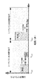
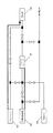
超大気圧反応器の一実施形態が、図3Aおよび図3Bに示される。成長反応器10は、外部圧力容器(図示せず)内に組み込まれてもよい。成長反応器10は、基板12の方向に反応性流体を輸送するフローチャネル26を含む。基板12は、例えばサファイア、炭化ケイ素、シリコン、または酸化亜鉛など、III族窒化物合金のエピタキシャル層の成長に適した任意の基板であってもよい。いくつかの例では、III族窒化物合金を含む第1のエピタキシャル層が堆積され、それにより、第2のエピタキシャル層の成長のための基板として機能する。他の実施形態では、III族窒化物合金を含む追加のエピタキシャル層が、後続のエピタキシャル層の成長のための基板として機能してもよい。基板12は基板キャリア18に取り付けられ、基板キャリア18は、基板12の成長表面がフローチャネル26の流れ方向に実質的に平行な平面内に位置するように基板12を保持する。成長表面での化学反応を最適化するための効果的なガス流反応速度および表面補給物質供給を提供するために、基板がフローチャネルに対して小さな傾斜角を有してもよい。
One embodiment of a superatmospheric reactor is shown in FIGS. 3A and 3B. The
シャフト16が、基板キャリア18に取り付けられてもよく、モータに機械的に連結されてもよく、それにより、基板キャリア18と基板12とが、成長表面の平面内で角度をもって回転する。本発明のいくつかの実施形態では、シャフト16は、好ましくは1〜20Hzの間の低い回転速度で基板12および基板キャリア18を回転させる。他の実施形態では、成長速度、表面化学反応、および/または被膜一様性を改良する必要が生じた場合および時にそのような必要性を満し得るように、より高い回転速度が使用されてもよい。したがって、一実施形態では、成長反応器10はさらに、基板キャリアを回転させるように適合されているデバイスを備えてもよい。
The shaft 16 may be attached to a
エピタキシャル層を成長させるための反応領域32が基板12の上方に備えられる。シャワーヘッド注入器24が、基板12とは反対側の反応領域32の上方に配置されてもよい。シャワーヘッド注入器24は、フローチャネル26に垂直な方向で基板の表面上に第2の組の反応性流体を注入するように適合されてもよい。シャワーヘッド注入器24は、一般には、第2の組の反応性流体を成長表面全体にわたって一様に分散させるように適合されてもよい。いくつかの実施形態では、シャワーヘッド注入器24は、多孔質ガラス、セラミック、または金属材料を含んでもよい。他の実施形態では、シャワーヘッド注入器24は、チャンバ22から反応領域32に延びる複数の管路を有する分散ブロックを備えてもよい。第2の組の反応性流体をチャンバ22に供給するために管路20が提供されてもよい。
A
いくつかの実施形態では、フローチャネル26を通して輸送される反応性流体は、限定はしないが、アンモニア[NH3]、ジメチルヒドラジン[(CH3)2N(NH2)]、またはt−ブチルアミン[(CH3)3CNH2]を含むV族前駆体であってもよい。第2の組の反応性流体は、限定はしないが、トリメチルインジウム[In(CH3)3](「TMI」)、トリメチルアルミニウム[Al(CH3)3](「TMA」)、またはトリメチルガリウム[Ga(CH3)3](「TMG」)など有機金属前駆体を含むIII族反応性前駆体を含んでもよい。反応性流体は、キャリアガスストリームに挿入されて、または液状で注入されて、反応領域または基板に輸送されてもよい。
In some embodiments, the reactive fluid transported through the
反応領域32の温度および基板12の温度は、加熱要素14を介して基板キャリア18に誘導的または伝導的に熱を加えることによって制御されてもよい。反応領域32の圧力は、成長反応器10と外部圧力容器との間のキャリアガスおよび不活性ガスの圧力を調節することによって制御し得る。安定した操作のために、成長反応器10と外部圧力容器との間で差圧制御を採用し得る。成長反応器10は、大気圧または大気圧未満で操作可能であってもよいが、好ましくは2〜100barの反応器圧力領域を含む超大気圧で操作させてもよい。さらに別の実施形態では、成長反応器10は、2〜30barの反応圧力領域内で操作させてもよい。
The temperature of the
第1の組の反応性流体を予熱できるようにするために、第2の加熱要素28が基板12の上流に備えられてもよい。この加熱要素は、第1の組の反応性流体の分解反応速度の独立制御を提供し得る。同様に、第2の組の反応性流体を予熱するために第3の加熱要素30が備えられてもよく、これは、第2の組の反応性流体の分解反応速度の制御を可能にする。加熱要素30は、フローチャネル26を通して注入される反応性流体には作用しないように反応領域32から隔離されてもよく、各組の反応性流体の分解反応速度の独立制御を可能にし得る。
A
図3Aおよび図3Bに示されるように、成長反応器10を周囲大気にさらすことなく成長反応器10に基板12を装入するためおよび/または成長反応器10から基板12を取り出すために、「ロードロック」システムが提供されてもよい。このシステムは、基板12を成長反応器10に挿入するか、または成長反応器10から取り出すための隔離チャンバ34を利用してもよい。
As shown in FIGS. 3A and 3B, in order to load and / or remove the
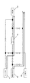
超大気圧反応器80の別の実施形態が図5に示されている。この実施形態では、基板キャリア86は、基板キャリア86を取り囲むRFコイル84によって、RF結合により誘導的に加熱されてもよい。第2の加熱器82は、反応性流体の流路に隣接して配置されてもよく、反応性流体が反応領域に達する前に反応性流体を加熱してもよい。
Another embodiment of a
成長法
別の態様では、基板上でエピタキシャル層およびヘテロ構造を成長させる方法が提供される。まず、基板キャリア上に配置されていてもよい基板の成長表面が、反応領域に対向する。その後、第1の反応性流体が、成長表面に平行な第1の流れ方向で反応領域内へ、成長表面全体にわたって成長表面の上方に供給されてもよく、第2の反応性流体が、第2の流れ方向で反応領域内へ成長表面上に供給されてもよく、ここで、第2の流れ方向は、第1の流れ方向から角度をずらされる。いかなる構造化学理論によっても制限されずに、次いで、第1の反応性流体および第2の反応性流体は、反応領域内で分解されて前駆体フラグメントとなってもよく、これらが次いで、成長表面に拡散し、基板の成長表面に化学吸着および/または物理吸着し得る。用語「角度をずらす」は、本明細書では流れ方向を特徴付けるために使用され、ある角度で交わってもよい流れベクトルを表す。
Growth Methods In another aspect, a method for growing epitaxial layers and heterostructures on a substrate is provided. First, the growth surface of the substrate, which may be arranged on the substrate carrier, faces the reaction region. Thereafter, a first reactive fluid may be supplied into the reaction region in a first flow direction parallel to the growth surface, over the growth surface, and above the growth surface. Two flow directions may be fed onto the growth surface into the reaction zone, where the second flow direction is offset in angle from the first flow direction. Without being limited by any structural chemistry theory, the first reactive fluid and the second reactive fluid may then be decomposed into precursor fragments within the reaction zone, which are then grown on the growth surface. And can be chemisorbed and / or physisorbed onto the growth surface of the substrate. The term “shift angle” is used herein to characterize the flow direction and represents a flow vector that may intersect at an angle.
いくつかの実施形態では、この方法はさらに、反応領域内で超大気圧を維持するステップを含む。いくつかの実施形態では、III族窒化物合金のエピタキシャル層の成長は、反応領域内で2〜100barの間の超大気圧で行われてもよい。別の実施形態では、III族窒化物合金のエピタキシャル層の成長は、反応領域内で2〜30barの間の超大気圧で行われてもよい。一般には、成長反応器の圧力は、キャリアガスを所望の圧力および流量で反応領域内に供給することによって維持し得る。 In some embodiments, the method further comprises maintaining a superatmospheric pressure within the reaction zone. In some embodiments, the growth of the III-nitride alloy epitaxial layer may be performed at superatmospheric pressures between 2 and 100 bar in the reaction region. In another embodiment, the growth of the III-nitride alloy epitaxial layer may be performed at superatmospheric pressure between 2 and 30 bar in the reaction region. In general, the growth reactor pressure can be maintained by supplying a carrier gas into the reaction zone at the desired pressure and flow rate.
後でより詳細に論じるように、いくつかの実施形態では、反応領域の圧力、およびキャリアガスと反応性流体との総体積流量は、特定のIII族窒化物合金のエピタキシャル被膜成長中に一定に保たれるように制御し得る。これを達成するために、反応領域内の全体の流速が一定に保たれるように反応性流体をキャリアガスに挿入してもよい。挿入および注入スキームは、反応領域を通るキャリアガスと反応性流体との総体積流量の変動を防止するように厳密に制御し得る。したがって、反応性流体のパルスは、操作圧力でパルスが占める体積に実質的に等しいキャリアガスの体積部分に取って代わる。成長させるべきIII族窒化物合金の各特定のエピタキシャル層が、異なる圧力領域を必要としてもよい。異なる圧力領域で成長させる異なるIII族窒化物合金間の遷移は、制御された圧力遷移領域を利用することによって達成してもよく、この圧力遷移領域では、成長するエピタキシャル層の品質に影響を及ぼす可能性のある圧力変動を生じることなく、圧力が増加/減少する。 As will be discussed in more detail later, in some embodiments, the pressure in the reaction region, and the total volume flow rate of the carrier gas and reactive fluid are constant during the epitaxial film growth of a particular group III-nitride alloy. It can be controlled to be kept. To accomplish this, a reactive fluid may be inserted into the carrier gas so that the overall flow rate in the reaction zone is kept constant. The insertion and injection scheme can be tightly controlled to prevent variations in the total volume flow rate of the carrier gas and reactive fluid through the reaction region. Thus, the pulse of reactive fluid replaces a volume of carrier gas that is substantially equal to the volume occupied by the pulse at the operating pressure. Each particular epitaxial layer of group III nitride alloy to be grown may require a different pressure region. Transitions between different Group III-nitride alloys grown in different pressure regions may be achieved by utilizing a controlled pressure transition region, which affects the quality of the growing epitaxial layer The pressure increases / decreases without causing possible pressure fluctuations.
いくつかの実施形態では、この方法はさらに、第1の反応性流体および第2の反応性流体を反応領域に供給しながら反応領域内で成長表面を回転させるステップを含む。回転は、成長表面にわたる反応性流体の一様な分散を実現する助けとなり得る。 In some embodiments, the method further includes rotating the growth surface within the reaction zone while supplying the first reactive fluid and the second reactive fluid to the reaction zone. Rotation can help achieve uniform distribution of the reactive fluid across the growth surface.
さらに、いくつかの実施形態では、この方法は、前記第1の反応性流体と第2の反応性流体とが実質的に同時に反応領域内に存在するように、第1の時点で第1の反応性流体を反応器内に注入するステップと、第2の時点で第2の反応性流体を反応器内に注入するステップとを含む。用語「実質的に同時」は、反応性流体の相対的な到着時間を表すために本明細書で使用するとき、たとえ、反応性流体の一方が反応領域内に先に到着しても、または他方の反応性流体よりも長い期間にわたって反応領域内に存在しても、第1の反応性流体と第2の反応性流体とが同時に反応領域内に存在することを概して意味する。いくつかの実施形態では、この方法はさらに、反応領域内での気相成分および/または反応性流体の組成をリアルタイムで監視および制御するステップを含む。 Further, in some embodiments, the method includes the first reactive fluid at the first time point such that the first reactive fluid and the second reactive fluid are present in the reaction zone at substantially the same time. Injecting a reactive fluid into the reactor and injecting a second reactive fluid into the reactor at a second time point. The term “substantially simultaneous” as used herein to denote the relative arrival time of a reactive fluid, even if one of the reactive fluids arrives first in the reaction region, or It generally means that the first reactive fluid and the second reactive fluid are present in the reaction region at the same time, even if they exist in the reaction region for a longer period of time than the other reactive fluid. In some embodiments, the method further includes monitoring and controlling the composition of the gas phase components and / or reactive fluid in the reaction zone in real time.
いくつかの実施形態では、第1の組の反応性流体と第2の組の反応性流体とが、III族反応性流体とV族反応性流体とを交互に含む。 In some embodiments, the first set of reactive fluids and the second set of reactive fluids comprise alternating Group III and Group V reactive fluids.
再び図3Aを参照すると、この方法は、第1の組の反応性流体を、成長表面に平行な流れ方向で反応領域32へ、基板12の成長表面全体にわたって成長表面の上方に輸送するステップを含んでもよい。例えば、第1の組の反応性流体は、図3Aおよび図3Bに示されるようにフローチャネル26を通して反応領域32に輸送されてもよい。第2の組の反応性流体は、第2の流れ方向で反応領域32内へ基板12の成長表面上に注入されてもよい。例えば、第2の組の反応性流体は、図3Aに示されるように密結合シャワーヘッド注入器24を通して反応領域32内に注入されてもよい。第2の流れ方向は、第1の組の反応性流体の流れ方向に実質的に垂直であってもよい。
Referring again to FIG. 3A, the method includes transporting a first set of reactive fluids to the
いくつかの実施形態では、反応性流体は、タイミングパルスとして反応領域32内に注入されてもよい(すなわち成分ガスの流束が時間的に制御される)。図3Aおよび図3Bの成長反応器10は、そのような注入方法に特に十分適し得る。
In some embodiments, the reactive fluid may be injected into the
図4は、共通の流路内に反応性流体が注入されるパルス注入スキームを示す。読者は、例示として、図3の成長反応器10のフローチャネル26を通して各反応性流体が交互のパルスとして注入されることを想定することができよう。図4に示されるように、TMIのパルスがキャリアガスストリーム(例えばN2)に注入され、その後、アンモニアのパルスが注入されてもよい。この例では、総ガス流量(キャリアガスと挿入された反応性流体との和)、および反応領域内の圧力を常に一定に保ってもよい。
FIG. 4 shows a pulse injection scheme in which reactive fluid is injected into a common flow path. The reader may assume by way of example that each reactive fluid is injected as alternating pulses through the
所定の期間後、各反応成分は、反応領域および基板12の成長表面に達する。パルスが注入器から基板12に輸送される間に、フローチャネル26の境界での流速の低下によりパルスが広がっていてもよい。これにより、アンモニアとTMIとがどちらもフローチャネル26内に存在する本例の場合などには、挿入された反応性流体パルスがいくらか重なり合ってもよく、したがって、反応性流体が基板12に達する前に反応性流体に関与する気相反応が生じてもよい。
After a predetermined period, each reaction component reaches the reaction region and the growth surface of the
III族反応性流体とV族反応性流体とを異なる経路を通して反応領域32に注入することによって、図3Aおよび図3Bの成長反応器10を、エピタキシャル層が製造される条件を厳密に制御するのに十分適したものにし得ることを理解すべきである。例えば、反応性流体(例えばIII族およびV族反応性流体)の注入経路の分離は、フローチャネル26内での反応性流体の反応の可能性を大幅に減少させる、または完全になくすことができ、最適なパルスのタイミングおよび/またはより狭いパルスの間隔での各反応性流体の導入を可能にし得る。これは、各パルスでの反応性流体材料の使用の最適化、およびより速い成長速度を実現できるようにし得る。
By injecting the Group III and V reactive fluids into the
いくつかの実施形態では、反応領域の圧力、および反応器を通る反応性流体とキャリアガスとの総体積流量は、特定の成分の被膜/合金配置の成長プロセス全体を通じて一定のままにし得る。反応器を通る実質的に一定の総体積流量、実質的に一定の平均流速、および/または実質的に一定の反応領域内の圧力を維持するようにキャリアガスの流量のバランスを取りながら、反応器内に反応性流体の計量されたパルスを注入するために、制御システムが提供されてもよい。したがって、反応性流体は、計量されたパルスとしてキャリアガスストリームに注入してもよく、各パルスの持続時間と振幅とを計量してもよい。パルスの振幅は、パルス中の反応性流体の平均体積流量に対応し、持続時間と振幅との積が、そのパルスに関する反応性流体の総体積に相当する。さらに、各パルスは、所定の時間だけ後続のパルスと間隔を空けてもよく、この時間中はキャリアガスのみが反応器内に注入される。これらの制御パラメータ(持続時間、振幅、および/または間隔)はそれぞれ、各層の合金およびその組成の所定のプロセスパラメータに応じて自動的に調節および制御され得る。したがって、本発明によって行われる方法の一実施形態は、反応領域内での気体成分の組成的および空間的分布をリアルタイムで監視および制御するステップを含む。 In some embodiments, the pressure in the reaction zone, and the total volume flow of reactive fluid and carrier gas through the reactor, may remain constant throughout the growth process of a particular component coating / alloy configuration. The reaction while balancing the carrier gas flow rate to maintain a substantially constant total volume flow through the reactor, a substantially constant average flow rate, and / or a substantially constant pressure in the reaction zone. A control system may be provided to inject metered pulses of reactive fluid into the vessel. Accordingly, the reactive fluid may be injected into the carrier gas stream as metered pulses, and the duration and amplitude of each pulse may be metered. The amplitude of the pulse corresponds to the average volume flow of the reactive fluid during the pulse, and the product of duration and amplitude corresponds to the total volume of reactive fluid for that pulse. In addition, each pulse may be spaced from a subsequent pulse by a predetermined time during which only carrier gas is injected into the reactor. Each of these control parameters (duration, amplitude, and / or interval) can be automatically adjusted and controlled depending on the predetermined process parameters of each layer alloy and its composition. Accordingly, one embodiment of the method performed by the present invention includes monitoring and controlling the compositional and spatial distribution of gaseous components within the reaction zone in real time.
制御システム
別の態様では、超大気圧成長条件を使用する半導体品質ヘテロ構造を成長させるための制御システムが提供されてもよい。制御システムは、基板上で被膜を成長させるための反応領域を有する成長反応器内への第1および第2の反応性流体の注入を制御してもよい。制御システムは、超大気圧反応器にキャリアガスを供給するように適合されているキャリアガス源と、超大気圧反応器に複数の反応性流体を供給するように適合されている複数の反応性流体源とを備え、反応性流体源は、超大気圧反応器に第1の反応性流体を供給するように適合されている第1の反応性流体源と、超大気圧反応器に第2の反応性流体を供給するように適合されている第2の反応性流体源とを含む。また、複数のアクチュエータを提供してもよく、それらは、超大気圧反応器に第1の組の反応性流体を流すための第1のアクチュエータと、超大気圧反応器への第2の組の反応性流体の流れを開始および停止するための第2のアクチュエータとを含む。また、反応領域内での実質的に一定の圧力と、反応領域を通る総体積流量とを維持しながら、第1の組の反応性流体と第2の組の反応性流体とをキャリアガスに挿入する複数のアクチュエータを制御するために、制御装置が提供されてもよく、構成されてもよい。
Control System In another aspect, a control system for growing semiconductor quality heterostructures using superatmospheric growth conditions may be provided. The control system may control the injection of the first and second reactive fluids into a growth reactor having a reaction region for growing a film on the substrate. The control system includes a carrier gas source adapted to supply a carrier gas to the superatmospheric reactor and a plurality of reactive fluid sources adapted to supply a plurality of reactive fluids to the superatmospheric reactor. And the reactive fluid source is adapted to supply a first reactive fluid to the superatmospheric reactor and a second reactive fluid to the superatmospheric reactor. And a second reactive fluid source adapted to supply the second reactive fluid source. A plurality of actuators may also be provided, the first actuator for flowing a first set of reactive fluids in the superatmospheric reactor and a second set of reactions to the superatmospheric reactor. And a second actuator for starting and stopping the flow of the sexual fluid. Also, the first set of reactive fluids and the second set of reactive fluids are used as carrier gases while maintaining a substantially constant pressure in the reaction zone and a total volume flow through the reaction zone. A control device may be provided or configured to control a plurality of actuators to be inserted.
いくつかの実施形態では、制御システムは、非反応段階で、キャリアガスを第1の一定の体積流量で反応領域を通して供給するように構成されてもよく、第1の一定の体積流量は前記総体積流量に実質的に等しい。反応段階の間、反応領域を通過するキャリアガスの体積流量は、反応領域を通過する反応性流体の体積流量を相殺するように減少されてもよい。さらに、制御システムは、約2bar〜約100bar、または約2bar〜約30barの反応領域内での一定の圧力を維持するように構成されてもよい。本明細書で使用するとき、用語「一定の圧力」と「実質的に一定の圧力」は、交換可能に使用されてもよく、基板上で被膜を成長させるときに反応領域内の圧力が大幅には変化または変動しない方法およびシステムを概して表す。したがって、反応領域内の圧力が、非反応段階の間(すなわちキャリアガスのみが反応領域を通して供給されるとき)に、反応段階の間(すなわち反応性流体がキャリアガスに挿入されるとき)と同じであるか、または約0.01bar未満だけ異なる場合に、反応領域の圧力が「実質的に一定」である。 In some embodiments, the control system may be configured to supply a carrier gas at a first constant volumetric flow rate through the reaction zone in a non-reactive phase, wherein the first constant volumetric flow rate is the total constant flow rate. It is substantially equal to the volume flow rate. During the reaction phase, the volume flow of the carrier gas through the reaction zone may be reduced to offset the volume flow of the reactive fluid through the reaction zone. Furthermore, the control system may be configured to maintain a constant pressure in the reaction zone of about 2 bar to about 100 bar, or about 2 bar to about 30 bar. As used herein, the terms “constant pressure” and “substantially constant pressure” may be used interchangeably, and the pressure in the reaction zone is greatly increased when a film is grown on a substrate. Generally represents methods and systems that do not change or vary. Thus, the pressure in the reaction zone is the same during the non-reaction phase (ie when only the carrier gas is fed through the reaction zone) and during the reaction phase (ie when the reactive fluid is inserted into the carrier gas). Or differ by less than about 0.01 bar, the pressure in the reaction zone is “substantially constant”.
いくつかの実施形態では、制御システムは、III族およびV族反応性流体を反応器に注入するために使用してもよい。 In some embodiments, the control system may be used to inject Group III and Group V reactive fluids into the reactor.
反応性流体のパルスをキャリアガスストリームに注入するための制御システムが図9A〜図9Eに示されている。制御システムは、流体回路を通って反応器100に向かうキャリアガス(例えば窒素)および反応性流体の流れを制御するために複数の弁を含む。あるいは、複数の弁の機能を模した回転シリンダ注入器または他のタイプのマニホルドなど、より洗練された機械的な注入システムが同等物として使用されてもよい。キャリアガスは、プッシュガス供給源104および圧縮ガス供給源108から回路に供給されてもよい。プッシュガス供給源104は、反応器100のための所定の流量に合う十分な流量でキャリアガスを回路に供給してもよい。圧縮ガス供給源108は、反応領域内での所要の圧力を維持するため、および/または流体回路の一部を加圧するために必要とされるときに、必要に応じてキャリアガスを回路に供給し得る。図9A〜図9Eに示される制御システムは、キャリアガスに反応ガスのパルスを挿入するための1つの可能な制御システムを例示する意図のものにすぎないことに留意すべきである。本明細書に記載する方法を実施するために、キャリアガスストリームに反応性流体を挿入するための様々な他の流体回路構成を使用してもよい。
A control system for injecting a pulse of reactive fluid into a carrier gas stream is shown in FIGS. 9A-9E. The control system includes a plurality of valves to control the flow of carrier gas (eg, nitrogen) and reactive fluid toward the
図9Aは、デフォルト位置で複数の弁が開放または閉鎖されているときの、キャリアガスと反応性流体との流路を制御し得る1つの可能な弁制御構成を示す。この構成では、一定の流量のキャリアガスを反応器100に供給し得、一方、反応性流体は、排出口に向けて流路を定め得る。
FIG. 9A illustrates one possible valve control configuration that can control the flow path of carrier gas and reactive fluid when multiple valves are open or closed in the default position. In this configuration, a constant flow of carrier gas can be supplied to the
反応性流体の「パルス」を準備するために、図9Bの流路によって示されるように弁を開閉してもよい。キャリアガスの流れは変わらないが、反応性流体の流れは、チャージリザーバ102(供給物貯留器102)を備える流体回路を開くように弁を開閉することによって流路を画定し直してもよく、チャージリザーバ102は、反応器100に供給されるキャリアガスに、厳密に計量された体積の反応性流体を含めるまたは挿入するように構成されてもよい。回路がパージされた直後、図9Cに示されるように、前駆体供給源106からの所定の体積および圧力の反応性流体をチャージリザーバ102に満たすように弁を閉じてもよい。所定の体積の反応性流体がチャージリザーバ102に供給された後、図9Dに示されるように、圧縮ガス供給源108からのキャリアガスで反応性流体の体積を圧縮し得、プッシュガス供給源104によって供給される反応器領域100および流体回路の圧力に厳密に一致させ得る。
To prepare a “pulse” of reactive fluid, the valve may be opened and closed as shown by the flow path in FIG. 9B. Although the carrier gas flow does not change, the reactive fluid flow may redefine the flow path by opening and closing a valve to open a fluid circuit comprising the charge reservoir 102 (feed reservoir 102); The
チャージリザーバ102内の反応性流体のパルスを反応器100に供給するために、図9Eに示されるように、チャージリザーバ102を通して反応器100に流れを向けるように適切な弁を開閉することによって、プッシュガス供給源104からのキャリアガス流の流路を画定し直してもよい。キャリアガスは、反応器100への反応性流体のパルスを、反応領域に向けて搬送し、反応領域内で反応性流体は別の反応性流体と反応してもよい。
To supply a pulse of reactive fluid in the
ここで、反応性流体の連続パルスを反応器100に供給するために必要に応じて前述のプロセスを繰り返してもよいことを理解すべきである。さらに、チャージリザーバ102は、様々なレベルに充填して、反応器100の反応器領域に供給される反応性流体パルスの体積濃度を変えてもよい。また、パルスの振幅または体積流量を変えるために、プッシュガス供給源104からのキャリアガスの一部がチャージリザーバ102を迂回してもよい。
It should now be understood that the above process may be repeated as necessary to supply a continuous pulse of reactive fluid to the
制御システムは、プログラム可能な制御装置を含んでもよく、これは、プログラム可能なスケジュールに従って弁を作動させる。例えば、制御装置は、パルス持続時間、パルス振幅、およびパルス間隔の前述のパラメータの制御を提供し得る。 The control system may include a programmable controller that operates the valves according to a programmable schedule. For example, the controller may provide control of the aforementioned parameters of pulse duration, pulse amplitude, and pulse interval.
さらに、高度なリアルタイム光学診断(例えばUV−VIS−IR、FTIR、ラマン分光法)を制御装置と一体化させてもよく、制御装置への入力として、エピタキシャル被膜のリアルタイム特性データおよび閉ループフィードバック制御データを提供する。そのような特性解析プロセスおよび制御法は、V. Woods and N. Dietz. InN growth by high-pressures chemical vapor deposition: Real-time optical growth characterization, Mater. Sci. & Eng. B 127(2-3) pp 239-250 (2006)、I. P. Herman, Optical Diagnositcs for thin Film Processing (Academic Press Inc., New York, 1996)、D. E, Aspnes and N. Dietz, Optical Approaches for Controlling Epitaxial Growth, Applied Surface Science 130-132 pp. 367-376 (1998)、およびN. Dietz, Real-time optical Characterization of thin film growth, Mater. Sci. & Eng. B87(l), pp.1 - 22 (2001)に概して記載されている。 In addition, advanced real-time optical diagnostics (e.g. UV-VIS-IR, FTIR, Raman spectroscopy) may be integrated with the controller, and as input to the controller, real-time characteristic data of the epitaxial film and closed-loop feedback control data. I will provide a. Such characterization processes and control methods are described in V. Woods and N. Dietz. InN growth by high-pressures chemical vapor deposition: Real-time optical growth characterization, Mater. Sci. & Eng. B 127 (2-3) pp 239-250 (2006), IP Herman, Optical Diagnositcs for thin Film Processing (Academic Press Inc., New York, 1996), D. E, Aspnes and N. Dietz, Optical Approaches for Controlling Epitaxial Growth, Applied Surface Science 130 -132 pp. 367-376 (1998) and N. Dietz, Real-time optical Characterization of thin film growth, Mater. Sci. & Eng. B87 (l), pp. 1-22 (2001) ing.
本発明を説明してきたが、インジウムリッチIII族窒化物合金の成長への本発明の適用例を説明するために以下の実施例を提示する。これらの具体的な実施例および組成物は、III族窒化物またはヘテロ構造に関する範囲を限定する意図のものではない。本明細書に記載する方法、反応器、および制御システムは、酸化物ベースの誘電体または他の化合物の半導体など、被膜合金成分の分圧が大きく異なる任意の材料系に適用し得る。 Having described the invention, the following examples are presented to illustrate the application of the invention to the growth of indium-rich group III-nitride alloys. These specific examples and compositions are not intended to limit the scope for Group III nitrides or heterostructures. The methods, reactors, and control systems described herein may be applied to any material system that has significantly different partial pressures of coating alloy components, such as oxide-based dielectrics or other compound semiconductors.
実施例1:ガスおよび表面反応化学の制御
上記のHPCVD反応器について、UV−Vis吸光分光法など様々な吸光分光法を利用して、成長表面の上方での気相成分の反応速度を分析し得る。いくつかの分析法が、V. Woods and N. Dietz, InN growth by high-pressures chemical vapor deposition: Real-time optical growth characterization, Mater. Sci. & Eng. B 127(2-3) pp.239-250 (2006)に、より詳細に記載されている。
Example 1: Control of Gas and Surface Reaction Chemistry For the above HPCVD reactor, various absorption spectroscopy methods such as UV-Vis absorption spectroscopy were used to analyze the reaction rate of gas phase components above the growth surface. obtain. Several analytical methods are described in V. Woods and N. Dietz, InN growth by high-pressures chemical vapor deposition: Real-time optical growth characterization, Mater. Sci. & Eng. B 127 (2-3) pp.239- 250 (2006).
図6は、InGaN成長中に使用される代表的な反応性流体流束注入スキームと、定常状態のInGaN成長条件下において、222.8nmで成長表面の上方で監視されるリアルタイムUV−Vis吸収波形とを例示する。この実施例では、TMI反応性流体とTMG反応性流体とを同時に注入した。 FIG. 6 shows a typical reactive fluid flux injection scheme used during InGaN growth and a real-time UV-Vis absorption waveform monitored above the growth surface at 222.8 nm under steady state InGaN growth conditions. Is illustrated. In this example, a TMI reactive fluid and a TMG reactive fluid were injected simultaneously.
グラフの上部は、反応性流体とキャリアガスとの前駆体流束(前駆体フラックス)を時間に対して示す。このグラフに示されるように、反応器を通る総体積流量は、注入サイクルシーケンスを通じて一定のままであった。3つの注入サイクルが示される。各サイクルは、キャリアガスに挿入されたNH3のパルスで始まった。パルスの幅は、パルスの持続時間(この実施例では1.5秒)を表し、パルス内の面積は、キャリアガスに挿入されるNH3の総体積を表す。NH3のパルスの後に、キャリアガスのみを反応器内に注入する期間が続いた。その直後、第2の反応性流体、すなわちTMIおよびTMGのパルスをキャリアガスに注入した。NH3およびTMI/TMGのパルス間の期間は、パルス間隔と呼ばれてもよい。第2のパルス間隔を、TMI/TMGの注入と次のNH3のパルスとの間に設けた。NH3の次の注入は、新たな注入サイクルの開始を示した。 The upper part of the graph shows the precursor flux (precursor flux) of the reactive fluid and the carrier gas with respect to time. As shown in this graph, the total volume flow through the reactor remained constant throughout the injection cycle sequence. Three injection cycles are shown. Each cycle began with a pulse of NH 3 inserted into the carrier gas. The width of the pulse represents the duration of the pulse (1.5 seconds in this example) and the area within the pulse represents the total volume of NH 3 inserted into the carrier gas. The NH 3 pulse was followed by a period in which only the carrier gas was injected into the reactor. Immediately thereafter, a pulse of the second reactive fluid, namely TMI and TMG, was injected into the carrier gas. The period between NH 3 and TMI / TMG pulses may be referred to as a pulse interval. A second pulse interval was provided between the TMI / TMG injection and the next NH 3 pulse. The next injection of NH 3 indicated the start of a new injection cycle.
図6のグラフの下部は、反応性流体が特性吸収を示す波長(この例ではλmax=222.8nm)でのリアルタイムでのUV吸収波形を示す。成長表面の上方への反応性流体の到着は、UV−Vis波形で観察することができ、各反応性流体成分に相関させることができる。リアルタイムUV−Vis波形解析を利用するグラフ上部の注入シーケンスの制御は、気相および表面反応の厳密な設計を可能にし、これは、プロセス条件を最適化するために不可欠な要素である。成長条件を最適化するために、反応性流体間のパルス間隔および各反応性流体パルスの長さの調節をプロセス制御パラメータとして使用してもよい。 The lower part of the graph of FIG. 6 shows the UV absorption waveform in real time at a wavelength where the reactive fluid exhibits characteristic absorption (λ max = 222.8 nm in this example). The arrival of the reactive fluid above the growth surface can be observed with a UV-Vis waveform and can be correlated to each reactive fluid component. Control of the injection sequence at the top of the graph utilizing real-time UV-Vis waveform analysis allows for rigorous design of gas phase and surface reactions, which is an essential element for optimizing process conditions. To optimize growth conditions, adjustment of the pulse interval between reactive fluids and the length of each reactive fluid pulse may be used as process control parameters.
図7に示されるように、さらなる別のプロセス制御パラメータを提供するために、TMIとTMGとを個別のパルスとして注入してもよい。個別のパルス注入は、InAlGaNなど三元合金の成長に特に有益であり得る。特に、そのような成長スキームは、相分離を制御するため、また、準単分子層のレベルでのTMIとTMGとの異なる成長化学を補償するために、三元InGaN合金形成について採用されてもよい。例えば、各シーケンスを、形成される合金のガスおよび表面化学に合わせて独特に調整してもよく、例えば各シーケンスはパルス間隔について独特のタイミングを有することができる。また、前駆体パルス長を調節することによって、各シーケンスが、特定の分圧に調整された独特のV/III族反応性流体比率を有することができる。各シーケンスを複数回繰り返して、特定量の材料を堆積して目標の材料組成物を形成してもよく、さらに、各シーケンスを調節して、材料合金化/混合プロセス、異なる材料の相分離プロセス、または2次元および3次元ナノ複合材、量子ドット、もしくは量子井戸の形成に対処してもよい。 As shown in FIG. 7, TMI and TMG may be injected as separate pulses to provide additional process control parameters. Individual pulse implantation may be particularly beneficial for the growth of ternary alloys such as InAlGaN. In particular, such growth schemes may be employed for ternary InGaN alloy formation to control phase separation and to compensate for the different growth chemistry of TMI and TMG at the quasi-monolayer level. Good. For example, each sequence may be uniquely tailored to the gas and surface chemistry of the alloy being formed, for example, each sequence may have a unique timing for the pulse interval. Also, by adjusting the precursor pulse length, each sequence can have a unique group V / III reactive fluid ratio adjusted to a specific partial pressure. Each sequence may be repeated multiple times to deposit a specific amount of material to form the target material composition, and each sequence can be adjusted to material alloying / mixing process, phase separation process of different materials Or the formation of 2D and 3D nanocomposites, quantum dots, or quantum wells.
実施例2:HPCVDによるInGaN成長
HPCVDによって成長させたIn1-xGaxN層の構造的特性についての初期の結果を図8に示す。図8は、同じ成長温度で、15barの反応器圧力で成長させたIn1-xGaxN層のX線回折(XRD)結果を示す。ガリウム組成は、x=0.0、0.04、0.09、0.18、0.31、および0.63で変えた。成長温度は、x=0.4よりも小さいx値に関しては一定に保ち、x=0.63に関しては50℃上げた。InGaN(0002)ブラッグ反射の位置および半値全幅(FWHM)が、成長した層の組成および構造品質に関する尺度である。本明細書で使用するとき、「構造品質」は、FWHMによって測定されるエピタキシャル層の結晶完全度を表す。LEDについて、良好な構造品質は、約200秒未満のFWHMによって表される。LDについて、良好な構造品質は、約50秒未満のFWHMによって表される。二元InN合金(x=0.0)は、200秒未満のFWHMを有するInN(0002)ブラッグ反射を有し、MBE成長層について報告されておりLEDで使用するのに適した値と同様の値であった。図7に示されるように、ガリウムの導入を増加するにつれて、より高い2Θ値へ移行するInGaN(0002)ブラッグ反射(格子定数の減少)、およびブラッグ反射のFWHMの増加が観察された。
Example 2: InGaN growth by HPCVD The initial results for the structural properties of In 1-x Ga x N layers grown by HPCVD are shown in FIG. FIG. 8 shows the X-ray diffraction (XRD) results of an In 1-x Ga x N layer grown at the same growth temperature and with a reactor pressure of 15 bar. The gallium composition was varied at x = 0.0, 0.04, 0.09, 0.18, 0.31, and 0.63. The growth temperature was kept constant for x values less than x = 0.4 and increased by 50 ° C. for x = 0.63. The position and full width at half maximum (FWHM) of the InGaN (0002) Bragg reflection is a measure for the composition and structural quality of the grown layer. As used herein, “structural quality” refers to the crystal perfection of an epitaxial layer as measured by FWHM. For LEDs, good structural quality is represented by a FWHM of less than about 200 seconds. For LD, good structural quality is represented by a FWHM of less than about 50 seconds. The binary InN alloy (x = 0.0) has an InN (0002) Bragg reflection with a FWHM of less than 200 seconds and is similar to a value suitable for use in LEDs reported for MBE growth layers. Value. As shown in FIG. 7, with increasing gallium incorporation, an InGaN (0002) Bragg reflection (decrease in lattice constant) transitioning to a higher 2Θ value and an increase in Bragg reflection FWHM were observed.
x=0.1からx=0.30の範囲内のガリウム濃度について、異なる組成の異なる相の存在を示す2つのブラッグ反射が観察された。しかし、サファイア基板上で成長させた同じ組成範囲内のInGaN層は、InGaN(0002)ブラッグ反射によって示したときに単相挙動を示した。 Two Bragg reflections were observed indicating the presence of different phases of different compositions for gallium concentrations in the range of x = 0.1 to x = 0.30. However, InGaN layers within the same composition range grown on sapphire substrates showed single-phase behavior when demonstrated by InGaN (0002) Bragg reflection.
実施例3:反応器圧力と成長温度との関係
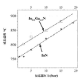
InNおよびIn0.85Ga0.15Nについての成長温度と反応器圧力との関係に関する初期の結果が図10に示される。図10に示されるように、InNについての可能な成長温度は、約6.6℃/barで増加させることができ、20barの反応器圧力で約880℃のInN成長温度になる。x=0.15でのIn1-xGaxNについて、(圧力の増加の線形関数としての成長温度の増加によって表される)傾きはわずかに減少し、約6.0℃/barとなる。図10に示される反応器圧力と共に増加する成長温度は、広い組成範囲(x)でIn1-xGaxNエピタキシャル層を一体化しなければならないIn1-xGaxNデバイス構造の成長についてのHPCVDの利益を示している。
Example 3 Relationship between Reactor Pressure and Growth Temperature Initial results regarding the relationship between growth temperature and reactor pressure for InN and In 0.85 Ga 0.15 N are shown in FIG. As shown in FIG. 10, the possible growth temperature for InN can be increased at about 6.6 ° C./bar, resulting in an InN growth temperature of about 880 ° C. at a reactor pressure of 20 bar. For In 1-x Ga x N at x = 0.15, the slope (represented by an increase in growth temperature as a linear function of pressure increase) decreases slightly to about 6.0 ° C./bar. . The growth temperature increasing with reactor pressure shown in FIG. 10 is for growth of In 1-x Ga x N device structures that must integrate In 1-x Ga x N epitaxial layers with a wide composition range (x). It shows the benefits of HPCVD.
以上、本発明を説明してきたが、同じ方法を多くの様式で変形し得ることは明らかである。そのような変形は、本発明の趣旨および範囲からの逸脱とみなすべきではなく、当業者に明らかな修正形態はすべて、添付の特許請求の範囲の範囲内に含まれるものと意図される。 Although the present invention has been described above, it is clear that the same method can be modified in many ways. Such variations are not to be regarded as a departure from the spirit and scope of the invention, and all modifications apparent to those skilled in the art are intended to be included within the scope of the appended claims.
Claims (40)
前記第1の層の上にあり接触する第2のIII族窒化物合金を含む第2のエピタキシャル層と
を備え、
前記第1のIII族窒化物合金は、前記第2のIII族窒化物合金が大気圧で堆積する最低温度において、大気圧で分解する合金であり、
前記第1のIII族窒化物合金は、超大気圧、および前記第2のIII族窒化物合金が堆積する温度では分解しない合金である
熱力学的に安定な半導体ヘテロ構造。 A first epitaxial layer comprising a first group III nitride alloy;
A second epitaxial layer comprising a second III-nitride alloy overlying and in contact with the first layer;
The first group III nitride alloy is an alloy that decomposes at atmospheric pressure at the lowest temperature at which the second group III nitride alloy deposits at atmospheric pressure;
The first group III nitride alloy is a thermodynamically stable semiconductor heterostructure that is an alloy that does not decompose at superatmospheric pressure and the temperature at which the second group III nitride alloy is deposited.
フローチャネル成長反応器内部で反応領域内に基板を保持するように適合されている基板キャリアと、
エピタキシャル層を成長させるための前記基板上の成長表面と、
第1の組の反応性流体の流れを、前記成長表面の上方の第1の流れ方向に沿って向けるように適合されているフローチャネルと、
前記反応領域に隣接する注入器と
を備え、前記注入器が、前記反応領域内に第2の組の反応性流体を注入するように適合され、それにより、前記第2の組の反応性流体が前記第1の組の反応性流体と反応するか、または分解して反応生成物の被膜を前記成長表面上に堆積する
反応器装置。 An enclosure capable of confining a pressure of up to about 100 bar;
A substrate carrier adapted to hold the substrate in the reaction region within the flow channel growth reactor;
A growth surface on the substrate for growing an epitaxial layer;
A flow channel adapted to direct a flow of a first set of reactive fluids along a first flow direction above the growth surface;
An injector adjacent to the reaction zone, the injector being adapted to inject a second set of reactive fluids into the reaction zone, whereby the second set of reactive fluids Reactor apparatus that reacts with or decomposes with the first set of reactive fluids to deposit a film of reaction product on the growth surface.
第1の組の反応性流体を、前記成長表面に実質的に平行な第1の流れ方向で前記反応領域内へ前記成長表面全体にわたって供給するステップと、
第2の組の反応性流体を、第2の流れ方向で前記反応領域内へ、前記成長表面上に供給するステップであって、前記第2の流れ方向が、前記第1の流れ方向に対して角度をずらされるステップと、
前記成長表面上でエピタキシャル層を形成するために、前記第1の組の反応性流体と前記第2の組の反応性流体とを前記反応領域内で反応させる又は分解するステップと
を含む方法。 Providing a growth surface in the reaction region;
Supplying a first set of reactive fluids across the growth surface into the reaction region in a first flow direction substantially parallel to the growth surface;
Supplying a second set of reactive fluids onto the growth surface in a second flow direction into the reaction region, wherein the second flow direction is relative to the first flow direction. Step to shift the angle,
Reacting or decomposing the first set of reactive fluids and the second set of reactive fluids in the reaction region to form an epitaxial layer on the growth surface.
前記超大気圧反応器に複数の反応性流体を供給するように適合されている複数の反応性流体源であって、前記超大気圧反応器に第1の組の反応性流体を供給するように適合されている第1の反応性流体源と、前記超大気圧反応器に第2の組の反応性流体を供給するように適合されている第2の反応性流体源とを含む複数の反応性流体源と、
前記第1の組の反応性流体の前記超大気圧反応器への流れを開始、停止、または変調するための第1のアクチュエータと、前記第2の組の反応性流体の前記超大気圧反応器への流れを開始、停止、または変調するための第2のアクチュエータとを含む複数のアクチュエータと、
前記超大気圧反応器内部にある成長表面を備える反応領域と、
前記反応領域内での実質的に一定の圧力と、前記反応領域を通る総体積流量とを維持しながら、前記第1の組の反応性流体と前記第2の組の反応性流体とを前記キャリアガスに挿入するために前記複数のアクチュエータを制御するように構成された制御装置と
を備える制御システム。 A carrier gas source adapted to supply a carrier gas to the superatmospheric pressure reactor;
A plurality of reactive fluid sources adapted to supply a plurality of reactive fluids to the superatmospheric reactor, adapted to supply a first set of reactive fluids to the superatmospheric reactor. A plurality of reactive fluids including a first reactive fluid source being adapted and a second reactive fluid source adapted to supply a second set of reactive fluids to the superatmospheric pressure reactor The source,
A first actuator for initiating, stopping, or modulating the flow of the first set of reactive fluids to the superatmospheric reactor, and the second set of reactive fluids to the superatmospheric reactor. A plurality of actuators including a second actuator for starting, stopping or modulating the flow of
A reaction zone comprising a growth surface inside the superatmospheric pressure reactor;
Maintaining the first set of reactive fluids and the second set of reactive fluids while maintaining a substantially constant pressure in the reaction zone and a total volume flow through the reaction zone; A control system configured to control the plurality of actuators for insertion into a carrier gas.
Applications Claiming Priority (2)
| Application Number | Priority Date | Filing Date | Title |
|---|---|---|---|
| US23323809P | 2009-08-12 | 2009-08-12 | |
| US61/233,238 | 2009-08-12 |
Related Parent Applications (1)
| Application Number | Title | Priority Date | Filing Date |
|---|---|---|---|
| JP2015105648A Division JP6358983B2 (en) | 2009-08-12 | 2015-05-25 | High pressure chemical vapor deposition apparatus, method, and composition produced thereby |
Publications (1)
| Publication Number | Publication Date |
|---|---|
| JP2017108155A true JP2017108155A (en) | 2017-06-15 |
Family
ID=43586489
Family Applications (3)
| Application Number | Title | Priority Date | Filing Date |
|---|---|---|---|
| JP2012524873A Pending JP2013502079A (en) | 2009-08-12 | 2010-08-12 | High pressure chemical vapor deposition apparatus, method, and composition produced thereby |
| JP2015105648A Expired - Fee Related JP6358983B2 (en) | 2009-08-12 | 2015-05-25 | High pressure chemical vapor deposition apparatus, method, and composition produced thereby |
| JP2017019410A Pending JP2017108155A (en) | 2009-08-12 | 2017-02-06 | High pressure chemical vapor deposition apparatuses and methods, and compositions produced therewith |
Family Applications Before (2)
| Application Number | Title | Priority Date | Filing Date |
|---|---|---|---|
| JP2012524873A Pending JP2013502079A (en) | 2009-08-12 | 2010-08-12 | High pressure chemical vapor deposition apparatus, method, and composition produced thereby |
| JP2015105648A Expired - Fee Related JP6358983B2 (en) | 2009-08-12 | 2015-05-25 | High pressure chemical vapor deposition apparatus, method, and composition produced thereby |
Country Status (5)
| Country | Link |
|---|---|
| US (2) | US9243329B2 (en) |
| EP (1) | EP2464760A4 (en) |
| JP (3) | JP2013502079A (en) |
| KR (1) | KR20120085743A (en) |
| WO (1) | WO2011019920A1 (en) |
Families Citing this family (4)
| Publication number | Priority date | Publication date | Assignee | Title |
|---|---|---|---|---|
| US10707082B2 (en) * | 2011-07-06 | 2020-07-07 | Asm International N.V. | Methods for depositing thin films comprising indium nitride by atomic layer deposition |
| WO2013032406A1 (en) * | 2011-09-01 | 2013-03-07 | National University Of Singapore | A system and a method for depositing a layer on a substrate |
| KR101960763B1 (en) | 2016-11-03 | 2019-03-21 | 주식회사 유진테크 | Method for manufacturing an epitaxial layer in low temperature |
| US11885018B2 (en) | 2018-09-24 | 2024-01-30 | Lehigh University | High pressure spatial chemical vapor deposition system and related process |
Citations (15)
| Publication number | Priority date | Publication date | Assignee | Title |
|---|---|---|---|---|
| JPS60126821A (en) * | 1983-12-14 | 1985-07-06 | Matsushita Electric Ind Co Ltd | Sample heating device, normal pressure cvd device and vacuum cvd device |
| JPH06216030A (en) * | 1992-03-06 | 1994-08-05 | Pioneer Electron Corp | Vapor growth device for compound semiconductor |
| JPH07235505A (en) * | 1993-12-28 | 1995-09-05 | Matsushita Electric Ind Co Ltd | Crystal growth method of semiconductor layer |
| JPH0856015A (en) * | 1994-08-12 | 1996-02-27 | Matsushita Electric Ind Co Ltd | Formation of semiconductor thin film |
| JPH09192479A (en) * | 1995-11-17 | 1997-07-29 | Toshio Goto | Plasma treating device and method therefor |
| JPH09283799A (en) * | 1996-04-09 | 1997-10-31 | Mitsubishi Cable Ind Ltd | Semiconductor light-emitting element |
| JPH1174566A (en) * | 1997-08-29 | 1999-03-16 | Mitsubishi Materials Corp | Multi-color luminous element |
| EP0979882A1 (en) * | 1998-08-13 | 2000-02-16 | Sony Corporation | Method of manufacturing a nitride series III-V group compound semiconductor |
| JP2001119106A (en) * | 1999-10-21 | 2001-04-27 | Matsushita Electric Ind Co Ltd | Method for manufacturing nitride semiconductor device |
| JP2003297765A (en) * | 2002-04-04 | 2003-10-17 | Lintec Co Ltd | Fluid-vaporizing device and film-forming device |
| JP2004146726A (en) * | 2002-10-28 | 2004-05-20 | Matsushita Electric Ind Co Ltd | Method and system for vapor phase growth |
| JP2004165445A (en) * | 2002-11-13 | 2004-06-10 | Furukawa Co Ltd | Semiconductor manufacturing arrangement |
| JP2006351974A (en) * | 2005-06-17 | 2006-12-28 | Chiba Univ | Semiconductor function element |
| JP2007531256A (en) * | 2004-03-27 | 2007-11-01 | アイクストロン、アーゲー | Method and apparatus for depositing metal oxide etc. by discharging discontinuous precursors |
| JP2008053669A (en) * | 2006-08-23 | 2008-03-06 | Ir Inc | Crystal growing method, and device using temperature-controlled process gas |
Family Cites Families (31)
| Publication number | Priority date | Publication date | Assignee | Title |
|---|---|---|---|---|
| US3608519A (en) | 1968-12-31 | 1971-09-28 | Texas Instruments Inc | Deposition reactor |
| US3675619A (en) | 1969-02-25 | 1972-07-11 | Monsanto Co | Apparatus for production of epitaxial films |
| US3745969A (en) | 1971-04-19 | 1973-07-17 | Motorola Inc | Offset top ejection vapor deposition apparatus |
| US4155784A (en) | 1977-04-08 | 1979-05-22 | Trw Inc. | Process for epitaxially growing a gallium arsenide layer having reduced silicon contaminants on a gallium arsenide substrate |
| FR2591616A1 (en) | 1985-12-17 | 1987-06-19 | Labo Electronique Physique | REACTOR CHAMBER FOR EPITAXIAL GROWTH IN STEAM PHASE OF SEMICONDUCTOR MATERIALS. |
| FR2599558B1 (en) * | 1986-05-27 | 1988-09-02 | Labo Electronique Physique | METHOD FOR PRODUCING A SEMICONDUCTOR DEVICE, INCLUDING THE DEPOSITION IN VAPOR PHASE OF LAYERS ON A SUBSTRATE |
| JP2704181B2 (en) * | 1989-02-13 | 1998-01-26 | 日本電信電話株式会社 | Method for growing compound semiconductor single crystal thin film |
| US5015330A (en) | 1989-02-28 | 1991-05-14 | Kabushiki Kaisha Toshiba | Film forming method and film forming device |
| JPH03257182A (en) | 1990-03-07 | 1991-11-15 | Hitachi Ltd | Surface processing device |
| US5433169A (en) * | 1990-10-25 | 1995-07-18 | Nichia Chemical Industries, Ltd. | Method of depositing a gallium nitride-based III-V group compound semiconductor crystal layer |
| JP2628404B2 (en) * | 1990-10-25 | 1997-07-09 | 日亜化学工業株式会社 | Semiconductor crystal film growth method |
| JP3875298B2 (en) * | 1995-12-27 | 2007-01-31 | シャープ株式会社 | Semiconductor light emitting device and manufacturing method thereof |
| US5684309A (en) * | 1996-07-11 | 1997-11-04 | North Carolina State University | Stacked quantum well aluminum indium gallium nitride light emitting diodes |
| US6233265B1 (en) * | 1998-07-31 | 2001-05-15 | Xerox Corporation | AlGaInN LED and laser diode structures for pure blue or green emission |
| US6459100B1 (en) * | 1998-09-16 | 2002-10-01 | Cree, Inc. | Vertical geometry ingan LED |
| JP2000164513A (en) | 1998-11-26 | 2000-06-16 | Sony Corp | Method for growing iii-v nitride compound semiconductor and manufacture of semiconductor element |
| JP4757976B2 (en) * | 2000-01-20 | 2011-08-24 | 士郎 酒井 | GaN compound semiconductor manufacturing method |
| US6548333B2 (en) * | 2000-12-01 | 2003-04-15 | Cree, Inc. | Aluminum gallium nitride/gallium nitride high electron mobility transistors having a gate contact on a gallium nitride based cap segment |
| US6906352B2 (en) * | 2001-01-16 | 2005-06-14 | Cree, Inc. | Group III nitride LED with undoped cladding layer and multiple quantum well |
| US6958497B2 (en) * | 2001-05-30 | 2005-10-25 | Cree, Inc. | Group III nitride based light emitting diode structures with a quantum well and superlattice, group III nitride based quantum well structures and group III nitride based superlattice structures |
| EP1424724A4 (en) | 2001-08-14 | 2007-10-24 | Powdec Kk | Chemical vapor phase epitaxial device |
| GB2392170A (en) * | 2002-08-23 | 2004-02-25 | Sharp Kk | MBE growth of a semiconductor layer structure |
| EP1400835B1 (en) * | 2002-09-17 | 2011-11-16 | Nippon Telegraph And Telephone Corporation | Semiconductor optical modulator and laser with such optical modulator |
| US20050178336A1 (en) | 2003-07-15 | 2005-08-18 | Heng Liu | Chemical vapor deposition reactor having multiple inlets |
| US7170111B2 (en) * | 2004-02-05 | 2007-01-30 | Cree, Inc. | Nitride heterojunction transistors having charge-transfer induced energy barriers and methods of fabricating the same |
| JP2005228757A (en) * | 2004-02-10 | 2005-08-25 | Japan Pionics Co Ltd | Apparatus and method for growing vapor phase |
| KR101181182B1 (en) * | 2004-11-11 | 2012-09-18 | 엘지이노텍 주식회사 | Light Emitting Device using nitrogen compound semiconductor and producing method thereof |
| US20080276860A1 (en) * | 2007-05-10 | 2008-11-13 | Burrows Brian H | Cross flow apparatus and method for hydride vapor phase deposition |
| US20080299411A1 (en) * | 2007-05-30 | 2008-12-04 | Oladeji Isaiah O | Zinc oxide film and method for making |
| CN101377009A (en) * | 2007-08-31 | 2009-03-04 | 富士迈半导体精密工业(上海)有限公司 | Semi-conducting material manufacturing apparatus |
| US10115859B2 (en) * | 2009-12-15 | 2018-10-30 | Lehigh University | Nitride based devices including a symmetrical quantum well active layer having a central low bandgap delta-layer |
-
2010
- 2010-08-12 JP JP2012524873A patent/JP2013502079A/en active Pending
- 2010-08-12 EP EP10808760.2A patent/EP2464760A4/en not_active Withdrawn
- 2010-08-12 US US13/390,055 patent/US9243329B2/en not_active Expired - Fee Related
- 2010-08-12 WO PCT/US2010/045329 patent/WO2011019920A1/en active Application Filing
- 2010-08-12 KR KR1020127006466A patent/KR20120085743A/en active Search and Examination
-
2015
- 2015-05-25 JP JP2015105648A patent/JP6358983B2/en not_active Expired - Fee Related
- 2015-12-29 US US14/982,132 patent/US10358743B2/en active Active
-
2017
- 2017-02-06 JP JP2017019410A patent/JP2017108155A/en active Pending
Patent Citations (17)
| Publication number | Priority date | Publication date | Assignee | Title |
|---|---|---|---|---|
| JPS60126821A (en) * | 1983-12-14 | 1985-07-06 | Matsushita Electric Ind Co Ltd | Sample heating device, normal pressure cvd device and vacuum cvd device |
| JPH06216030A (en) * | 1992-03-06 | 1994-08-05 | Pioneer Electron Corp | Vapor growth device for compound semiconductor |
| JPH07235505A (en) * | 1993-12-28 | 1995-09-05 | Matsushita Electric Ind Co Ltd | Crystal growth method of semiconductor layer |
| JPH0856015A (en) * | 1994-08-12 | 1996-02-27 | Matsushita Electric Ind Co Ltd | Formation of semiconductor thin film |
| JPH09192479A (en) * | 1995-11-17 | 1997-07-29 | Toshio Goto | Plasma treating device and method therefor |
| JPH09283799A (en) * | 1996-04-09 | 1997-10-31 | Mitsubishi Cable Ind Ltd | Semiconductor light-emitting element |
| JPH1174566A (en) * | 1997-08-29 | 1999-03-16 | Mitsubishi Materials Corp | Multi-color luminous element |
| JP2000058462A (en) * | 1998-08-13 | 2000-02-25 | Sony Corp | Manufacture of nitride based iii-v compound semiconductor |
| EP0979882A1 (en) * | 1998-08-13 | 2000-02-16 | Sony Corporation | Method of manufacturing a nitride series III-V group compound semiconductor |
| JP2001119106A (en) * | 1999-10-21 | 2001-04-27 | Matsushita Electric Ind Co Ltd | Method for manufacturing nitride semiconductor device |
| US20030143765A1 (en) * | 1999-10-21 | 2003-07-31 | Matsushita Electric Industrial Co., Ltd. | Method of fabricating nitride semiconductor device |
| JP2003297765A (en) * | 2002-04-04 | 2003-10-17 | Lintec Co Ltd | Fluid-vaporizing device and film-forming device |
| JP2004146726A (en) * | 2002-10-28 | 2004-05-20 | Matsushita Electric Ind Co Ltd | Method and system for vapor phase growth |
| JP2004165445A (en) * | 2002-11-13 | 2004-06-10 | Furukawa Co Ltd | Semiconductor manufacturing arrangement |
| JP2007531256A (en) * | 2004-03-27 | 2007-11-01 | アイクストロン、アーゲー | Method and apparatus for depositing metal oxide etc. by discharging discontinuous precursors |
| JP2006351974A (en) * | 2005-06-17 | 2006-12-28 | Chiba Univ | Semiconductor function element |
| JP2008053669A (en) * | 2006-08-23 | 2008-03-06 | Ir Inc | Crystal growing method, and device using temperature-controlled process gas |
Non-Patent Citations (1)
| Title |
|---|
| N.DIETZ: "InN growth by HPCVD:Real-time and ex-situ characterization", IMPERIAL COLLEGE PRESS, JPN7015000235, 2006, pages 204 - 235, ISSN: 0004199958 * |
Also Published As
| Publication number | Publication date |
|---|---|
| JP6358983B2 (en) | 2018-07-18 |
| KR20120085743A (en) | 2012-08-01 |
| JP2013502079A (en) | 2013-01-17 |
| EP2464760A4 (en) | 2013-08-28 |
| EP2464760A1 (en) | 2012-06-20 |
| WO2011019920A1 (en) | 2011-02-17 |
| US20160138191A1 (en) | 2016-05-19 |
| JP2015216381A (en) | 2015-12-03 |
| US20120138952A1 (en) | 2012-06-07 |
| US9243329B2 (en) | 2016-01-26 |
| US10358743B2 (en) | 2019-07-23 |
Similar Documents
| Publication | Publication Date | Title |
|---|---|---|
| KR101379410B1 (en) | Eqipment for high volume manufacture of group ⅲ-ⅴ semiconductor materials | |
| KR101353334B1 (en) | Abatement of reaction gases from gallium nitride deposition | |
| KR101330156B1 (en) | Gallium trichloride injection scheme | |
| Ozgit et al. | Atomic layer deposition of GaN at low temperatures | |
| US6569765B1 (en) | Hybrid deposition system and methods | |
| US8377803B2 (en) | Methods and systems for forming thin films | |
| US20080050889A1 (en) | Hotwall reactor and method for reducing particle formation in GaN MOCVD | |
| JP2017108155A (en) | High pressure chemical vapor deposition apparatuses and methods, and compositions produced therewith | |
| US8138069B2 (en) | Substrate pretreatment for subsequent high temperature group III depositions | |
| KR20090019851A (en) | High volume delivery system for gallium trichloride | |
| Beaumont et al. | Nitrogen precursors in metalorganic vapor phase epitaxy of (Al, Ga) N | |
| JP6109657B2 (en) | Vapor growth apparatus and vapor growth method | |
| FR2968831A1 (en) | METHODS OF FORMING NITRIDE III MASSIVE MATERIALS ON METAL NITRIDE GROWTH MATRIX LAYERS AND STRUCTURES FORMED THEREFROM | |
| JP2004524690A (en) | Hybrid growth system and method | |
| JPH1017400A (en) | Method for magnesium-doped nitride type iii-v group compound semiconductor crystal | |
| JP2008218760A (en) | Manufacturing method for semiconductor device, and manufacturing apparatus for semiconductor device | |
| JP2004363456A (en) | Method and apparatus for manufacturing semiconductor device | |
| Woelk et al. | III-Nitride multiwafer MOCVD systems for blue-green LED material | |
| Tokunaga et al. | Multiwafer atmospheric‐pressure MOVPE reactor for nitride semiconductors and ex‐situ dry cleaning of reactor components using chlorine gas for stable operation | |
| Matsumoto et al. | High growth rate MOVPE | |
| Schreiner et al. | Growth of GaN, AlGaN and AlN Layers for LED Manufacturing: Investigations on Growth Conditions using a “Hotwall” MOCVD System | |
| KR101365224B1 (en) | Micro control device and method for the growth of thin film | |
| JP2007063096A (en) | Gas phase growth device and gas phase growth method | |
| Yu et al. | Characterization of AlXGa1-xN Grown by MOCVD at Low Temperatures | |
| JPH01179312A (en) | Vapor growth of iii-v compound semiconductor |
Legal Events
| Date | Code | Title | Description |
|---|---|---|---|
| A521 | Request for written amendment filed |
Free format text: JAPANESE INTERMEDIATE CODE: A523 Effective date: 20170303 |
|
| A621 | Written request for application examination |
Free format text: JAPANESE INTERMEDIATE CODE: A621 Effective date: 20170303 |
|
| A977 | Report on retrieval |
Free format text: JAPANESE INTERMEDIATE CODE: A971007 Effective date: 20171214 |
|
| A131 | Notification of reasons for refusal |
Free format text: JAPANESE INTERMEDIATE CODE: A131 Effective date: 20180122 |
|
| A601 | Written request for extension of time |
Free format text: JAPANESE INTERMEDIATE CODE: A601 Effective date: 20180423 |
|
| A521 | Request for written amendment filed |
Free format text: JAPANESE INTERMEDIATE CODE: A523 Effective date: 20180612 |
|
| A131 | Notification of reasons for refusal |
Free format text: JAPANESE INTERMEDIATE CODE: A131 Effective date: 20181204 |
|
| A601 | Written request for extension of time |
Free format text: JAPANESE INTERMEDIATE CODE: A601 Effective date: 20190304 |
|
| A521 | Request for written amendment filed |
Free format text: JAPANESE INTERMEDIATE CODE: A523 Effective date: 20190410 |
|
| A131 | Notification of reasons for refusal |
Free format text: JAPANESE INTERMEDIATE CODE: A131 Effective date: 20190821 |
|
| A601 | Written request for extension of time |
Free format text: JAPANESE INTERMEDIATE CODE: A601 Effective date: 20191121 |
|
| A521 | Request for written amendment filed |
Free format text: JAPANESE INTERMEDIATE CODE: A523 Effective date: 20200108 |
|
| A02 | Decision of refusal |
Free format text: JAPANESE INTERMEDIATE CODE: A02 Effective date: 20200127 |