JP2017103380A - Intelligent power module and electric vehicle or hybrid car - Google Patents
Intelligent power module and electric vehicle or hybrid car Download PDFInfo
- Publication number
- JP2017103380A JP2017103380A JP2015236365A JP2015236365A JP2017103380A JP 2017103380 A JP2017103380 A JP 2017103380A JP 2015236365 A JP2015236365 A JP 2015236365A JP 2015236365 A JP2015236365 A JP 2015236365A JP 2017103380 A JP2017103380 A JP 2017103380A
- Authority
- JP
- Japan
- Prior art keywords
- intelligent power
- power module
- module according
- power semiconductor
- circuit
- Prior art date
- Legal status (The legal status is an assumption and is not a legal conclusion. Google has not performed a legal analysis and makes no representation as to the accuracy of the status listed.)
- Granted
Links
Images


Classifications
-
- H—ELECTRICITY
- H02—GENERATION; CONVERSION OR DISTRIBUTION OF ELECTRIC POWER
- H02M—APPARATUS FOR CONVERSION BETWEEN AC AND AC, BETWEEN AC AND DC, OR BETWEEN DC AND DC, AND FOR USE WITH MAINS OR SIMILAR POWER SUPPLY SYSTEMS; CONVERSION OF DC OR AC INPUT POWER INTO SURGE OUTPUT POWER; CONTROL OR REGULATION THEREOF
- H02M7/00—Conversion of ac power input into dc power output; Conversion of dc power input into ac power output
- H02M7/003—Constructional details, e.g. physical layout, assembly, wiring or busbar connections
-
- B—PERFORMING OPERATIONS; TRANSPORTING
- B60—VEHICLES IN GENERAL
- B60L—PROPULSION OF ELECTRICALLY-PROPELLED VEHICLES; SUPPLYING ELECTRIC POWER FOR AUXILIARY EQUIPMENT OF ELECTRICALLY-PROPELLED VEHICLES; ELECTRODYNAMIC BRAKE SYSTEMS FOR VEHICLES IN GENERAL; MAGNETIC SUSPENSION OR LEVITATION FOR VEHICLES; MONITORING OPERATING VARIABLES OF ELECTRICALLY-PROPELLED VEHICLES; ELECTRIC SAFETY DEVICES FOR ELECTRICALLY-PROPELLED VEHICLES
- B60L50/00—Electric propulsion with power supplied within the vehicle
- B60L50/50—Electric propulsion with power supplied within the vehicle using propulsion power supplied by batteries or fuel cells
- B60L50/51—Electric propulsion with power supplied within the vehicle using propulsion power supplied by batteries or fuel cells characterised by AC-motors
-
- H—ELECTRICITY
- H01—ELECTRIC ELEMENTS
- H01L—SEMICONDUCTOR DEVICES NOT COVERED BY CLASS H10
- H01L25/00—Assemblies consisting of a plurality of individual semiconductor or other solid state devices ; Multistep manufacturing processes thereof
- H01L25/03—Assemblies consisting of a plurality of individual semiconductor or other solid state devices ; Multistep manufacturing processes thereof all the devices being of a type provided for in the same subgroup of groups H01L27/00 - H01L33/00, or in a single subclass of H10K, H10N, e.g. assemblies of rectifier diodes
- H01L25/10—Assemblies consisting of a plurality of individual semiconductor or other solid state devices ; Multistep manufacturing processes thereof all the devices being of a type provided for in the same subgroup of groups H01L27/00 - H01L33/00, or in a single subclass of H10K, H10N, e.g. assemblies of rectifier diodes the devices having separate containers
- H01L25/11—Assemblies consisting of a plurality of individual semiconductor or other solid state devices ; Multistep manufacturing processes thereof all the devices being of a type provided for in the same subgroup of groups H01L27/00 - H01L33/00, or in a single subclass of H10K, H10N, e.g. assemblies of rectifier diodes the devices having separate containers the devices being of a type provided for in group H01L29/00
- H01L25/115—Assemblies consisting of a plurality of individual semiconductor or other solid state devices ; Multistep manufacturing processes thereof all the devices being of a type provided for in the same subgroup of groups H01L27/00 - H01L33/00, or in a single subclass of H10K, H10N, e.g. assemblies of rectifier diodes the devices having separate containers the devices being of a type provided for in group H01L29/00 the devices being arranged next to each other
-
- H—ELECTRICITY
- H05—ELECTRIC TECHNIQUES NOT OTHERWISE PROVIDED FOR
- H05K—PRINTED CIRCUITS; CASINGS OR CONSTRUCTIONAL DETAILS OF ELECTRIC APPARATUS; MANUFACTURE OF ASSEMBLAGES OF ELECTRICAL COMPONENTS
- H05K7/00—Constructional details common to different types of electric apparatus
- H05K7/20—Modifications to facilitate cooling, ventilating, or heating
- H05K7/2089—Modifications to facilitate cooling, ventilating, or heating for power electronics, e.g. for inverters for controlling motor
- H05K7/209—Heat transfer by conduction from internal heat source to heat radiating structure
-
- H—ELECTRICITY
- H01—ELECTRIC ELEMENTS
- H01L—SEMICONDUCTOR DEVICES NOT COVERED BY CLASS H10
- H01L23/00—Details of semiconductor or other solid state devices
- H01L23/34—Arrangements for cooling, heating, ventilating or temperature compensation ; Temperature sensing arrangements
-
- H—ELECTRICITY
- H01—ELECTRIC ELEMENTS
- H01L—SEMICONDUCTOR DEVICES NOT COVERED BY CLASS H10
- H01L23/00—Details of semiconductor or other solid state devices
- H01L23/34—Arrangements for cooling, heating, ventilating or temperature compensation ; Temperature sensing arrangements
- H01L23/36—Selection of materials, or shaping, to facilitate cooling or heating, e.g. heatsinks
- H01L23/367—Cooling facilitated by shape of device
-
- H—ELECTRICITY
- H02—GENERATION; CONVERSION OR DISTRIBUTION OF ELECTRIC POWER
- H02M—APPARATUS FOR CONVERSION BETWEEN AC AND AC, BETWEEN AC AND DC, OR BETWEEN DC AND DC, AND FOR USE WITH MAINS OR SIMILAR POWER SUPPLY SYSTEMS; CONVERSION OF DC OR AC INPUT POWER INTO SURGE OUTPUT POWER; CONTROL OR REGULATION THEREOF
- H02M1/00—Details of apparatus for conversion
- H02M1/32—Means for protecting converters other than automatic disconnection
- H02M1/327—Means for protecting converters other than automatic disconnection against abnormal temperatures
-
- H—ELECTRICITY
- H02—GENERATION; CONVERSION OR DISTRIBUTION OF ELECTRIC POWER
- H02M—APPARATUS FOR CONVERSION BETWEEN AC AND AC, BETWEEN AC AND DC, OR BETWEEN DC AND DC, AND FOR USE WITH MAINS OR SIMILAR POWER SUPPLY SYSTEMS; CONVERSION OF DC OR AC INPUT POWER INTO SURGE OUTPUT POWER; CONTROL OR REGULATION THEREOF
- H02M7/00—Conversion of ac power input into dc power output; Conversion of dc power input into ac power output
- H02M7/42—Conversion of dc power input into ac power output without possibility of reversal
- H02M7/44—Conversion of dc power input into ac power output without possibility of reversal by static converters
- H02M7/48—Conversion of dc power input into ac power output without possibility of reversal by static converters using discharge tubes with control electrode or semiconductor devices with control electrode
- H02M7/53—Conversion of dc power input into ac power output without possibility of reversal by static converters using discharge tubes with control electrode or semiconductor devices with control electrode using devices of a triode or transistor type requiring continuous application of a control signal
- H02M7/537—Conversion of dc power input into ac power output without possibility of reversal by static converters using discharge tubes with control electrode or semiconductor devices with control electrode using devices of a triode or transistor type requiring continuous application of a control signal using semiconductor devices only, e.g. single switched pulse inverters
- H02M7/5387—Conversion of dc power input into ac power output without possibility of reversal by static converters using discharge tubes with control electrode or semiconductor devices with control electrode using devices of a triode or transistor type requiring continuous application of a control signal using semiconductor devices only, e.g. single switched pulse inverters in a bridge configuration
-
- H—ELECTRICITY
- H02—GENERATION; CONVERSION OR DISTRIBUTION OF ELECTRIC POWER
- H02P—CONTROL OR REGULATION OF ELECTRIC MOTORS, ELECTRIC GENERATORS OR DYNAMO-ELECTRIC CONVERTERS; CONTROLLING TRANSFORMERS, REACTORS OR CHOKE COILS
- H02P27/00—Arrangements or methods for the control of AC motors characterised by the kind of supply voltage
- H02P27/04—Arrangements or methods for the control of AC motors characterised by the kind of supply voltage using variable-frequency supply voltage, e.g. inverter or converter supply voltage
- H02P27/06—Arrangements or methods for the control of AC motors characterised by the kind of supply voltage using variable-frequency supply voltage, e.g. inverter or converter supply voltage using dc to ac converters or inverters
-
- Y—GENERAL TAGGING OF NEW TECHNOLOGICAL DEVELOPMENTS; GENERAL TAGGING OF CROSS-SECTIONAL TECHNOLOGIES SPANNING OVER SEVERAL SECTIONS OF THE IPC; TECHNICAL SUBJECTS COVERED BY FORMER USPC CROSS-REFERENCE ART COLLECTIONS [XRACs] AND DIGESTS
- Y02—TECHNOLOGIES OR APPLICATIONS FOR MITIGATION OR ADAPTATION AGAINST CLIMATE CHANGE
- Y02T—CLIMATE CHANGE MITIGATION TECHNOLOGIES RELATED TO TRANSPORTATION
- Y02T10/00—Road transport of goods or passengers
- Y02T10/60—Other road transportation technologies with climate change mitigation effect
- Y02T10/70—Energy storage systems for electromobility, e.g. batteries
Landscapes
- Engineering & Computer Science (AREA)
- Power Engineering (AREA)
- Microelectronics & Electronic Packaging (AREA)
- Physics & Mathematics (AREA)
- Condensed Matter Physics & Semiconductors (AREA)
- General Physics & Mathematics (AREA)
- Computer Hardware Design (AREA)
- Sustainable Development (AREA)
- Life Sciences & Earth Sciences (AREA)
- Sustainable Energy (AREA)
- Transportation (AREA)
- Mechanical Engineering (AREA)
- Thermal Sciences (AREA)
- Inverter Devices (AREA)
- Structures Or Materials For Encapsulating Or Coating Semiconductor Devices Or Solid State Devices (AREA)
- Cooling Or The Like Of Semiconductors Or Solid State Devices (AREA)
- Chemical & Material Sciences (AREA)
- Materials Engineering (AREA)
Abstract
Description
本実施の形態は、インテリジェントパワーモジュール、および電気自動車またはハイブリッドカーに関する。 The present embodiment relates to an intelligent power module and an electric vehicle or a hybrid car.
従来から、半導体モジュールの1つとして、絶縁ゲートバイポーラトランジスタ(IGBT)のような半導体デバイスを含むパワー素子(チップ)の外囲が樹脂でモールドされたパワー半導体モジュールが知られている。動作状態において、半導体デバイスは発熱するため、裏面側にヒートシンクやフィンなどの放熱器を配置して放熱させ、半導体デバイスを冷却するのが一般的である。 2. Description of the Related Art Conventionally, as one of semiconductor modules, a power semiconductor module in which a power element (chip) including a semiconductor device such as an insulated gate bipolar transistor (IGBT) is molded with resin is known. Since the semiconductor device generates heat in the operating state, it is general to dissipate heat by disposing a heat sink such as a heat sink or a fin on the back surface side to cool the semiconductor device.
また、放熱効果をより高めるために、冷却器を備え、冷却液を用いて冷却するようにしたパワー半導体モジュールも知られている。 In addition, there is also known a power semiconductor module that is provided with a cooler and is cooled by using a cooling liquid in order to enhance the heat dissipation effect.
本実施の形態は、放熱特性に優れ、モジュール化が容易であり、小型化にとって好適なインテリジェントパワーモジュール、および電気自動車またはハイブリッドカーを提供する。 The present embodiment provides an intelligent power module that is excellent in heat dissipation characteristics, easy to be modularized, and suitable for miniaturization, and an electric vehicle or a hybrid car.
本実施の形態の一態様によれば、半導体デバイスと、前記半導体デバイスの外囲を封止する封止体とを有するパワー半導体モジュールと、前記封止体上に搭載され、前記パワー半導体モジュールを駆動する駆動回路部と、前記封止体が装着されて、前記パワー半導体モジュールを冷却する冷却部とを備えるインテリジェントパワーモジュールが提供される。 According to one aspect of the present embodiment, a power semiconductor module having a semiconductor device and a sealing body that seals an outer periphery of the semiconductor device, and the power semiconductor module mounted on the sealing body, An intelligent power module is provided that includes a drive circuit unit that drives and a cooling unit that is mounted with the sealing body and cools the power semiconductor module.
本実施の形態の他の態様によれば、半導体デバイスと、前記半導体デバイスの外囲を封止する封止体とを有するパワー半導体モジュールと、前記封止体上に搭載され、前記パワー半導体モジュールを駆動する駆動回路部と、前記封止体が装着されて、前記パワー半導体モジュールを冷却する冷却部とを備え、前記パワー半導体モジュールがツーインワンモジュールを構成するように複数個配置されて、シックスインワンモジュールタイプのインバータまたはコンバータを構成するインテリジェントパワーモジュールが提供される。 According to another aspect of the present embodiment, a power semiconductor module having a semiconductor device and a sealing body that seals an outer periphery of the semiconductor device, and mounted on the sealing body, the power semiconductor module A plurality of power semiconductor modules are arranged to form a two-in-one module, and a six-in-one module is provided. An intelligent power module constituting a module type inverter or converter is provided.
本実施の形態の他の態様によれば、上記のインテリジェントパワーモジュールを搭載する電気自動車またはハイブリッドカーが提供される。 According to another aspect of the present embodiment, an electric vehicle or a hybrid car equipped with the intelligent power module is provided.
本実施の形態によれば、放熱特性に優れ、モジュール化が容易であり、小型化にとって好適なインテリジェントパワーモジュール、および電気自動車またはハイブリッドカーを提供することができる。 According to the present embodiment, it is possible to provide an intelligent power module that is excellent in heat dissipation characteristics, easy to be modularized, and suitable for miniaturization, and an electric vehicle or a hybrid car.
次に、図面を参照して、本実施の形態について説明する。以下に説明する図面の記載において、同一または類似の部分には同一または類似の符号を付している。ただし、平面図、側面図、底面図、断面図などは模式的なものであり、各構成部品の厚みと平面寸法との関係などは現実のものとは異なることに留意すべきである。したがって、具体的な厚みや寸法は以下の説明を参酌して判断すべきものである。また、図面の相互間においても互いの寸法の関係や比率が異なる部分が含まれていることは勿論である。 Next, the present embodiment will be described with reference to the drawings. In the following description of the drawings, the same or similar parts are denoted by the same or similar reference numerals. However, it should be noted that the plan view, the side view, the bottom view, the cross-sectional view, and the like are schematic, and the relationship between the thickness and the planar dimension of each component is different from the actual one. Therefore, specific thicknesses and dimensions should be determined in consideration of the following description. In addition, it is a matter of course that portions having different dimensional relationships and ratios are included between the drawings.
また、以下に示す実施の形態は、技術的思想を具体化するための装置や方法を例示するものであって、各構成部品の材質、形状、構造、配置などを特定するものではない。実施の形態は、特許請求の範囲内において、種々の変更を加えることができる。 Further, the embodiments described below exemplify apparatuses and methods for embodying the technical idea, and do not specify the material, shape, structure, arrangement, etc. of each component. The embodiment can be variously modified within the scope of the claims.
[第1の実施の形態]
(全体構成)
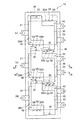
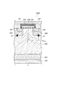
第1の実施の形態に係るインテリジェントパワーモジュール(IPM;Intelligent Power Module)10の平面構造は、図1に示すように表わされる。なお、図1では、一部(駆動回路部40など)を透過して示している。
[First Embodiment]
(overall structure)
A planar structure of an intelligent power module (IPM) 10 according to the first embodiment is expressed as shown in FIG. In FIG. 1, a part (the
図1に示すように、IPM10は、放熱板(例えば、アルミニウム(Al)製のヒートシンクまたはウォータージャケット(WJ)などの冷却器であっても良い)50と、放熱板50上に装着された複数個分のパワー半導体モジュール20(20A・20B・20C)と、パワー半導体モジュール20A・20B・20C上に共通に搭載された駆動回路部(例えば、FR−4、6層)40とで構成される。パワー半導体モジュール20A・20B・20Cは、放熱板50の上面(装着面)に配置された位置決め用の凸部52によって、装着する位置が予め規定される(図2〜図4参照)。
As shown in FIG. 1, the IPM 10 includes a heat sink (for example, a heat sink made of aluminum (Al) or a cooler such as a water jacket (WJ)) 50 and a plurality of pieces mounted on the
第1の実施の形態に係るIPM10は、例えば、パワー半導体モジュール20A・20B・20Cにツーインワン(2 in 1)タイプを採用することにより、シックスインワン(6 in 1)タイプのスイッチングモジュールを構成できる(詳細については、後述する)。スイッチングモジュールを構成するIPM10においては、パワー半導体モジュール20A・20B・20Cを効率よく冷却でき、過熱による劣化を抑えることが可能である。
The
ここで、第1の実施の形態に係るIPM10としては、図示を省略しているが、放熱板50と、放熱板50上に装着されたパワー半導体モジュール20と、パワー半導体モジュール20上に搭載された駆動回路部40とで構成されても良い。
Here, the IPM 10 according to the first embodiment is not illustrated, but is mounted on the
すなわち、第1の実施の形態に係るIPM10は、図示を省略している半導体デバイスの外囲を封止するパッケージ(封止体)21を有する、少なくとも1個のパワー半導体モジュール20と、パッケージ21上に配置され、パワー半導体モジュール20を駆動する駆動回路部40と、パッケージ21が装着されて、パワー半導体モジュール20の発熱を放熱する放熱板(冷却部)50とを備える。このような構成において、第1の実施の形態に係るIPM10は、放熱特性に優れ、モジュール化が容易であり、小型化にとって好適なものとすることができる。
That is, the IPM 10 according to the first embodiment includes at least one
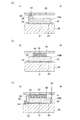
第1の実施の形態に係るIPM10において、パワー半導体モジュール20A・20B・20Cの模式的断面構造は、図2(a)、図2(b)および図3(a)〜図3(c)に示すように表わされる。なお、パワー半導体モジュール20A・20B・20Cは同一構造なので、ここでは、パワー半導体モジュール20Bを例に説明する。
In the
すなわち、図2(a)は、図1のIa−Ia線に沿うIPM10の模式的断面構造図を、図2(b)は、図1のIb−Ib線に沿うIPM10の模式的断面構造図を示し、図3(a)は、図1のIc−Ic線に沿うIPM10の模式的断面構造図を、図3(b)は、図1のId−Id線に沿うIPM10の模式的断面構造図を、図3(c)は、図1のIe−Ie線に沿うIPM10の模式的断面構造図を、それぞれ示すもので、パワー半導体モジュール20Bは、接合材26を介して、パッケージ21が放熱板50の上面の凸部52によって規定された枠内に接合される。
2A is a schematic cross-sectional structure diagram of the
接合材26としては、例えばサーマルコンパウンドまたは銀(Ag)ペーストなどの接合ペーストなどを用いることができる。特には、接合材26として、0.5W/mK〜300W/mKの熱伝導率を有するものが好ましく、例えばエポキシ樹脂、アクリル樹脂、シリコン樹脂、ウレタン樹脂、もしくはポリイミドなどのいずれかの有機物を単体で用いることができる。また、上記のいずれかの有機物に、金属粉または各種のセラミックス粉が混合された合成樹脂であっても良い。もしくは、加熱硬化させて使用する各種の半田や焼成銀などを、接合材26として用いても良い。
As the
パワー半導体モジュール20Bの上面には、放熱性を有するグリスやシリコン樹脂などの放熱性樹脂22を介して、金属(例えば、銅(Cu)またはAl)製の放熱プレート30が接合される。放熱プレート30は、図1および図3(c)に示すように、その両端部が金属や樹脂からなるネジ32によって放熱板50の上面にネジ止め固定される。この放熱プレート30の固定によって、パワー半導体モジュール20Bが放熱板50の上面に、より強固に接合される。
A
また、放熱プレート30と放熱板50とが強固に接合されることにより、パワー半導体モジュール20Bおよび駆動回路部40の高い放熱性が確保される。すなわち、パワー半導体モジュール20Bおよび駆動回路部40で発生した熱の一部は、放熱プレート30によって吸収された後、放熱板50より放熱される。
In addition, the
なお、放熱プレート30をネジ32によって固定させる際には、例えば接合材26などにより、放熱プレート30の両端部を放熱板50の上面に接合させるようにしても良い。
Note that when the
駆動回路部40は、2mm〜5mm程度の厚さを有するアルミナ(無機フィラー入り)などの樹脂製の放熱シート(または、放熱性を有するシリコン樹脂など)24を介して、放熱プレート30上に接合される。駆動回路部40は、図3(c)に示すパワー半導体モジュール20Bのリード端子S2のように、上方に折り曲げられた状態で挿通孔41内に挿通されることにより、リード端子(ゲート信号端子電極G1〜G6、ソース信号端子電極S1〜S6、ソースセンス端子SS1〜SS6)との接続が行われる。
The
すなわち、駆動回路部40は、パワー半導体モジュール20A・20B・20Cを駆動するための駆動回路が実装された駆動回路基板を、例えばモールド樹脂によってパッケージングしたものであって、リード端子が上方に折り曲げられた状態で挿通される挿通孔41を有する。
That is, the
なお、図示を省略しているが、挿通孔41に挿通されるリード端子としては、例えば、パワー半導体モジュール20A・20B・20Cが内蔵するサーミスタなどの温度測定用端子を含むものであっても良い。
In addition, although illustration is abbreviate | omitted, as a lead terminal inserted in the
駆動回路部40は、図1および図3(a)に示すように、例えば対角線の一方の線分上の2点において、金属や樹脂からなるネジ42によって、パッケージ21上の取付部28にネジ止め固定される。
As shown in FIGS. 1 and 3A, the
ここで、パワー半導体モジュール20A・20B・20Cの各パッケージ21の上面の対角線上の2点には、例えばモールド樹脂からなる取付部28が設けられ、その取付部28には、駆動回路部40をネジ42によって固定するための回路部取付穴44が設けられる。
Here, at two points on the diagonal line of the upper surface of each
放熱板50は、図4に示すように、パワー半導体モジュール20A・20B・20Cに対して共通に設けられる。放熱板50は、例えば、パワー半導体モジュール20A・20B・20Cの各パッケージ21の裏面側に露出する、ヒートスプレッダとしての銅プレート層(図示省略)に接合される。
As shown in FIG. 4, the
放熱板50上の、パワー半導体モジュール20A・20B・20Cが装着される個所には、それぞれ位置決め用の凸部52が設けられる。凸部52は、パッケージ21の各辺に沿うようにして周囲を囲む枠形状に配置される。
On the
凸部52は、パワー半導体モジュール20A・20B・20Cの位置決めのみでなく、放熱板50の剛性を高め、放熱板50のねじれを抑えると共に、接合時に接合材26の流出を防ぐ効果もある。
The
また、放熱板50上の、凸部52の枠外には、放熱プレート30の両端部をネジ32によってネジ止めするための取付穴(プレート取付穴)54が設けられる。
Further, outside the frame of the
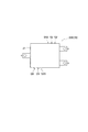
ここで、第1の実施の形態に係るIPM10に適用されるパワー半導体モジュール20(20A・20B・20C)は、図5に示すように、図示を省略したパワー素子(半導体デバイス)の外囲がパッケージ21によって方形状にモールドされた半導体パッケージ装置であって、ここでは一例として、3つの端子電極(P・N・O)を1本ずつ備えた3端子型構造を示している。
Here, in the power semiconductor module 20 (20A, 20B, 20C) applied to the
パワー半導体モジュール20Bの場合、例えばモールド樹脂からなるパッケージ21の、第1の辺に沿って設けられたドレイン端子電極Pおよび接地電位端子電極Nと、パッケージ21の第1の辺に対向する第3の辺に設けられた出力端子電極Oとを備える。
In the case of the
また、パッケージ21の第1、第3の辺と直交する第2の辺に沿って設けられたリード端子(G2・S2・SS2)と、第4の辺に沿って設けられたリード端子(G5・S5・SS5)とが、それぞれパッケージ21の外部に延出されている。すなわち、このパワー半導体モジュール20Bは、半導体デバイスQ2・Q5を内蔵した2 in 1タイプとなっている。
In addition, a lead terminal (G2, S2, SS2) provided along a second side orthogonal to the first and third sides of the
なお、図1に示したように、パワー半導体モジュール20Aの場合は、半導体デバイスQ1・Q4を内蔵した2 in 1タイプとなっており、ドレイン端子電極Pと接地電位端子電極Nと出力端子電極Oと、リード端子(G1・S1・SS1、G4・S4・SS4)とを備える。同様に、パワー半導体モジュール20Cの場合は、半導体デバイスQ3・Q6を内蔵した2 in 1タイプとなっており、ドレイン端子電極Pと接地電位端子電極Nと出力端子電極Oと、リード端子(G3・S3・SS3、G6・S6・SS6)とを備える。
As shown in FIG. 1, the
また、詳細については後述するが、パワー半導体モジュール20A・20B・20Cとしては、半導体デバイスが1チップから構成されるものに限定されないことは勿論であり、半導体デバイスの他にダイオードやサーミスタなどの電子部品を含むものであっても良い。
Further, although details will be described later, the
(適用例)
次に、第1の実施の形態に係るIPM10の適用例について説明する。
(Application example)
Next, an application example of the
図6は、第1の実施の形態に係るIPM10を、例えば、電気自動車またはハイブリッドカーのパワーコントロールユニットに搭載した場合を例示するものであって、駆動回路部40は、1次側回路部40aと2次側回路部40bとから構成される。
FIG. 6 illustrates a case where the
1次側回路部40aには、絶縁トランス105(1051 ・1052 ・1053 ・1054 ・1055 ・1056 )の1次コイル(L1)、スイッチレギュレータ101、LDO(Low Drop Out)102、温度モニタ回路106、短絡保護回路107、電圧降下検出回路108、および絶縁カプラ(フォトカプラ)109(1091 ・1092 ・1093 ・1094 ・1095 ・1096 )の受光部側が設けられる。絶縁トランス105の1次コイル(L1)は、スイッチレギュレータ101に共通に接続され、スイッチレギュレータ101およびLDO102は、例えば、電気自動車またはハイブリッドカーのバッテリ504に接続される。絶縁カプラ109の受光部側には、温度モニタ回路106、短絡保護回路107、および電圧降下検出回路108が共通に接続される。
The primary
2次側回路部40bには、絶縁トランス105の2次コイル(L2)、ゲートドライバ104、および絶縁カプラ109の発光部側が設けられる。絶縁トランス105の2次コイル(L2)は、ゲートドライバ104、温度モニタ回路106、短絡保護回路107、および電圧降下検出回路108に共通に接続される。絶縁カプラ109の発光部側には、ゲートドライバ104が接続される。
The secondary
ゲートドライバ104および温度モニタ回路106は、LDO102とパワー半導体モジュール20(20A・20B・20C)との間に接続される。また、ゲートドライバ104、温度モニタ回路106、短絡保護回路107、および電圧降下検出回路108は、電気自動車またはハイブリッドカーのECU(Engine Control Unit)502に接続される。
The
なお、ゲートドライバ104は、複数の高圧側のドライブ回路HS1・HS2・HS3と複数の低圧側のドライブ回路LS4・LS5・LS6とを有し、後述する電源回路から正負の電源が供給される。
The
このような構成を有する駆動回路部40の平面パターン構成(基板構成)は、図7(a)および図7(b)に示すように表わされる。なお、図7(a)は、駆動回路部40の表側(上面)43Sの平面パターン構成を示す概略図であり、図7(b)は、表側43Sの平面パターン構成を透過した状態で裏側(下面)43Bの平面パターン構成を示す概略図である。
The planar pattern configuration (substrate configuration) of the
すなわち、第1の実施の形態に係るIPM10に適用可能なパワー半導体モジュール20A・20B・20C上に搭載される駆動回路部40は、複数個のパワー半導体モジュール20A・20B・20Cに対して共通に設けられる。駆動回路部40は矩形形状を有し、長手方向に沿って配置された1次側回路部40aと、1次側回路部40aに隣接配置された2次側回路部40bとを備える。
That is, the
1次側回路部40aの表側43Sによって、上述のスイッチレギュレータ101およびLDO102を含む電源回路などが構成される。裏側43Bには、温度モニタ回路106、短絡保護回路107、および電圧降下検出回路108などが配置される。
The
2次側回路部40bでは、ゲートドライバ104の複数の高圧側のドライブ回路HS1・HS2・HS3と複数の低圧側のドライブ回路LS4・LS5・LS6とが交互に配置される。
In the
2次側回路部40bの各ドライブ回路HS1・HS2・HS3・LS4・LS5・LS6は、1次側回路部40aと2次側回路部40bとにまたがって配置された絶縁トランス1051 〜1056 をそれぞれに介して、1次側回路部40aの表側43Sの電源回路と共通に接続される。また、各ドライブ回路HS1・HS2・HS3・LS4・LS5・LS6は、1次側回路部40aと2次側回路部40bとにまたがって配置された絶縁カプラ1091 〜1096 をそれぞれに介して、1次側回路部40aの裏側43Bの温度モニタ回路106・短絡保護回路107・電圧降下検出回路108と共通に接続される。
The drive circuits HS1, HS2, HS3, LS4, LS5, and LS6 of the secondary
ここで、第1の実施の形態に係るIPM10を適用して構成され、例えば、電気自動車またはハイブリッドカーの3相交流モータ部(図示省略)を駆動するための、3相交流インバータ10Aの概略構成について説明する。この3相交流インバータ10Aは、半導体デバイスQ1〜Q6にSiC MOSFET(Silicon Carbide Metal Oxide Semiconductor Field Effect Transistor)を適用するようにした場合の例である。
Here, the schematic configuration of a three-
図8に示すように、3相交流インバータ10Aは、3相交流モータ部のU相、V相、W相に対応して、U相のインバータ(SiC MOSFET Q1・Q4)、V相のインバータ(SiC MOSFET Q2・Q5)、W相のインバータ(SiC MOSFET Q3・Q6)が接続されている。
As shown in FIG. 8, the three-
U相のインバータのSiC MOSFET Q1には、高圧側のドライブ回路HS1が、U相のインバータのSiC MOSFET Q4には、低圧側のドライブ回路LS4が、それぞれ接続される。同様に、V相のインバータのSiC MOSFET Q2には、高圧側のドライブ回路HS2が、V相のインバータのSiC MOSFET Q5には、低圧側のドライブ回路LS5が、それぞれ接続される。同様に、W相のインバータのSiC MOSFET Q3には、高圧側のドライブ回路HS3が、W相のインバータのSiC MOSFET Q6には、低圧側のドライブ回路LS6が、それぞれ接続される。 The high-voltage side drive circuit HS1 is connected to the SiC MOSFET Q1 of the U-phase inverter, and the low-voltage side drive circuit LS4 is connected to the SiC MOSFET Q4 of the U-phase inverter. Similarly, a high-voltage drive circuit HS2 is connected to the SiC MOSFET Q2 of the V-phase inverter, and a low-voltage drive circuit LS5 is connected to the SiC MOSFET Q5 of the V-phase inverter. Similarly, a high-voltage side drive circuit HS3 is connected to the SiC MOSFET Q3 of the W-phase inverter, and a low-voltage side drive circuit LS6 is connected to the SiC MOSFET Q6 of the W-phase inverter.
図9に示す3相交流インバータ10Bは、図8に示した3相交流インバータ10Aの回路構成をより詳細に示すもので、SiC MOSFET Q1〜Q6は、ボディダイオードBD1〜BD6をそれぞれ有する。また、SiC MOSFET Q1〜Q6のソース・ドレイン間には、フリーホイールダイオードDI1〜DI6がそれぞれ逆並列に接続されている。
A three-
なお、フリーホイールダイオードDI1〜DI6に代えて、例えばショットキーバリアダイオードをそれぞれ逆並列に接続するようにしても良い。 In place of the freewheel diodes DI1 to DI6, for example, Schottky barrier diodes may be connected in antiparallel.
(回路構成)
次に、第1の実施の形態に係るIPM10に適用可能なパワー半導体モジュール20の回路構成例について、より具体的に説明する。
(Circuit configuration)
Next, a circuit configuration example of the
ここでは、第1の実施の形態に係るIPM10に適用可能なパワー半導体モジュール20Aであって、2個の半導体デバイスQ1・Q4が1つのパッケージ21内にモールドされた半導体パッケージ装置、いわゆる2 in 1タイプのモジュールについて説明する。
Here, the
半導体デバイスQ1・Q4として、SiC MOSFETを適用した2 in 1モジュール120Aの回路構成は、例えば図10(a)に示すように表わされる。
A circuit configuration of a 2 in 1
すなわち、2 in 1モジュール120Aは、図10(a)に示すように、2個のSiC MOSFET Q1・Q4が1つのモジュールとして内蔵された、ハーフブリッジ内蔵モジュールの構成を備える。
That is, as shown in FIG. 10A, the 2 in 1
ここで、モジュールは、1つの大きなトランジスタとみなすことができるが、内蔵されているトランジスタが1チップまたは複数チップの場合がある。すなわち、モジュールには、1 in 1(ワンインワン)、2 in 1、4 in 1(フォーインワン)、6 in 1などがあり、例えば、1つのモジュール上において、2個分のトランジスタ(チップ)を内蔵したモジュールは2 in 1、2 in 1を2組み内蔵したモジュールは4 in 1、2 in 1を3組み内蔵したモジュールは6 in 1と呼ばれている。 Here, the module can be regarded as one large transistor, but the built-in transistor may be one chip or a plurality of chips. That is, the module includes 1 in 1 (one in one), 2 in 1, 4 in 1 (four in one), 6 in 1, etc. For example, two transistors (chips) are provided on one module. A built-in module is a module that incorporates two sets of 2 in 1, 2 in 1, and a module that incorporates three sets of 4 in 1, 2 in 1 is called 6 in 1.
図10(a)に示すように、2 in 1モジュール120Aは、2個のSiC MOSFET Q1・Q4と、SiC MOSFET Q1・Q4に逆並列接続されるダイオードDI1・DI4が1つのモジュールとして内蔵されている。図10(a)において、G1は、SiC MOSFET Q1のゲート信号端子電極であり、S1は、SiC MOSFET Q1のソース信号端子電極である。同様に、G4は、SiC MOSFET Q4のゲート信号端子電極であり、S4は、SiC MOSFET Q4のソース信号端子電極である。また、Pは、正側電源入力端子であり、Nは、負側電源入力端子であり、Oは、出力端子電極である。
As shown in FIG. 10A, the 2 in 1
また、第1の実施の形態に係るIPM10に適用可能なパワー半導体モジュール20Aであって、半導体デバイスQ1・Q4として、IGBT(Insulated Gate Bipolar Transistor)を適用した2 in 1モジュール120Bの回路構成は、図10(b)に示すように表わされる。
Further, the
図10(b)に示すように、2 in 1モジュール120Bは、2個のIGBT Q1・Q4と、IGBT Q1・Q4に逆並列接続されるダイオードDI1・DI4が1つのモジュールとして内蔵されている。図10(b)において、G1は、IGBT Q1のゲート信号端子電極であり、E1は、IGBT Q1のエミッタ端子電極である。同様に、G4は、IGBT Q4のゲート信号端子電極であり、E4は、IGBT Q4のエミッタ端子電極である。また、Pは、正側電源入力端子であり、Nは、負側電源入力端子であり、Oは、出力端子電極である。
As shown in FIG. 10B, the 2 in 1
第1の実施の形態に係るIPM10に適用可能なパワー半導体モジュール20Bに適用される半導体デバイスQ2・Q5、およびパワー半導体モジュール20Cに適用される半導体デバイスQ3・Q6についても同様であり、詳しい説明は省略する。
The same applies to the semiconductor devices Q2 and Q5 applied to the
(デバイス構造)
第1の実施の形態に係るIPM10に適用可能なパワー半導体モジュール20Aのデバイス構造であって、半導体デバイスQ1・Q4として適用されるSiC MOSFET 220Aの模式的断面構造は、図11(a)に示すように表わされ、IGBT 220Bの模式的断面構造は、図11(b)に示すように表わされる。
(Device structure)
A device structure of the
図11(a)に示すように、SiC MOSFET 220Aは、n- 高抵抗層からなる半導体基板226と、半導体基板226の表面側に形成されたpボディ領域228と、pボディ領域228の表面に形成されたソース領域230と、pボディ領域228間の半導体基板226の表面上に配置されたゲート絶縁膜232と、ゲート絶縁膜232上に配置されたゲート電極238と、ソース領域230およびpボディ領域228に接続されたソース電極234と、半導体基板226の表面と反対側の裏面に配置されたn+ ドレイン領域224と、n+ ドレイン領域224に接続されたドレイン電極236とを備える。
As shown in FIG. 11A, the
図11(a)において、SiC MOSFET 220Aは、プレーナゲート型のnチャネル縦型SiC MOSFETで構成されているが、後述する図15に示すように、nチャネル縦型SiC T(Trench) MOSFET 220Cなどで構成されていても良い。
In FIG. 11A, the
または、第1の実施の形態に係るIPM10に適用可能なパワー半導体モジュール20Aに適用される半導体デバイスQ1・Q4としては、SiC MOSFET 220Aの代わりに、GaN系FETなどを採用することもできる。
Alternatively, as the semiconductor devices Q1 and Q4 applied to the
第1の実施の形態に係るIPM10に適用可能なパワー半導体モジュール20Bに適用される半導体デバイスQ2・Q5、およびパワー半導体モジュール20Cに適用される半導体デバイスQ3・Q6についても同様である。
The same applies to the semiconductor devices Q2 and Q5 applied to the
さらには、第1の実施の形態に係るIPM10に適用可能なパワー半導体モジュール20に適用される半導体デバイスQ1〜Q6には、バンドギャップエネルギーが、例えば、1.1eV〜8eVの半導体を用いることができる。
Furthermore, the semiconductor devices Q1 to Q6 applied to the
同様に、第1の実施の形態に係るIPM10に適用可能なパワー半導体モジュール20Aであって、半導体デバイスQ1・Q4として適用されるIGBT 220Bは、図11(b)に示すように、n- 高抵抗層からなる半導体基板226と、半導体基板226の表面側に形成されたpボディ領域228と、pボディ領域228の表面に形成されたエミッタ領域230Eと、pボディ領域228間の半導体基板226の表面上に配置されたゲート絶縁膜232と、ゲート絶縁膜232上に配置されたゲート電極238と、エミッタ領域230Eおよびpボディ領域228に接続されたエミッタ電極234Eと、半導体基板226の表面と反対側の裏面に配置されたp+ コレクタ領域224Pと、p+ コレクタ領域224Pに接続されたコレクタ電極236Cとを備える。
Similarly, the
図11(b)において、IGBT 220Bは、プレーナゲート型のnチャネル縦型IGBTで構成されているが、トレンチゲート型のnチャネル縦型IGBTなどで構成されていても良い。
In FIG. 11B, the
第1の実施の形態に係るIPM10に適用可能なパワー半導体モジュール20Aに適用される半導体デバイスQ1・Q4の例であって、ソースパッド電極SP、ゲートパッド電極GPを含むSiC MOSFET 220Aの模式的断面構造は、図12に示すように表わされる。
FIG. 4 is an example of semiconductor devices Q1 and Q4 applied to the
ゲートパッド電極GPは、ゲート絶縁膜232上に配置されたゲート電極238に接続され、ソースパッド電極SPは、ソース領域230およびpボディ領域228に接続されたソース電極234に接続される。また、ゲートパッド電極GPおよびソースパッド電極SPは、図12に示すように、SiC MOSFET 220Aの表面を覆うパッシベーション用の層間絶縁膜244上に配置される。
Gate pad electrode GP is connected to
なお、ゲートパッド電極GPおよびソースパッド電極SPの下方の半導体基板226内には、図示していないが、図11(a)の中央部と同様に、微細構造のトランジスタ構造が形成されていても良い。
Although not shown in the
さらに、図12に示すように、中央部のトランジスタ構造においても、パッシベーション用の層間絶縁膜244上にソースパッド電極SPが延在して配置されていても良い。
Furthermore, as shown in FIG. 12, the source pad electrode SP may be extended and disposed on the passivation
第1の実施の形態に係るIPM10に適用可能なパワー半導体モジュール20Aに適用される半導体デバイスQ1・Q4の例であって、エミッタパッド電極EP、ゲートパッド電極GPを含むIGBT 220Bの模式的断面構造は、図13に示すように表わされる。
FIG. 4 is an example of semiconductor devices Q1 and Q4 applied to the
ゲートパッド電極GPは、ゲート絶縁膜232上に配置されたゲート電極238に接続され、エミッタパッド電極EPは、エミッタ領域230Eおよびpボディ領域228に接続されたエミッタ電極234Eに接続される。また、ゲートパッド電極GPおよびエミッタパッド電極EPは、図13に示すように、IGBT 220Bの表面を覆うパッシベーション用の層間絶縁膜244上に配置される。
Gate pad electrode GP is connected to
なお、ゲートパッド電極GPおよびエミッタパッド電極EPの下方の半導体基板226内には、図示していないが、図11(b)の中央部と同様に、微細構造のIGBT構造が形成されていても良い。
Note that although not shown in the
さらに、図13に示すように、中央部のIGBT構造においても、パッシベーション用の層間絶縁膜244上にエミッタパッド電極EPが延在して配置されていても良い。
Further, as shown in FIG. 13, even in the IGBT structure in the central portion, the emitter pad electrode EP may be arranged to extend on the
第1の実施の形態に係るIPM10に適用可能なパワー半導体モジュール20Bに適用される半導体デバイスQ2・Q5、およびパワー半導体モジュール20Cに適用される半導体デバイスQ3・Q6についても同様である。
The same applies to the semiconductor devices Q2 and Q5 applied to the
半導体デバイスQ1〜Q6としては、SiC DI(Double Implanted) MOSFET、SiC T MOSFETなどのSiC系パワーデバイス、あるいはGaN系高電子移動度トランジスタ(HEMT: High Electron Mobility Transistor)などのGaN系パワーデバイスを適用可能である。また、場合によっては、Si系MOSFETやIGBTなどのパワーデバイスも適用可能である。 As the semiconductor devices Q1 to Q6, SiC power devices such as SiC DI (Double Implanted) MOSFET and SiC T MOSFET, or GaN power devices such as GaN high electron mobility transistors (HEMT) are applied. Is possible. In some cases, power devices such as Si-based MOSFETs and IGBTs are also applicable.
―SiC DI MOSFET―
第1の実施の形態に係るIPM10に適用可能なパワー半導体モジュール20に適用される半導体デバイスの例であって、SiC DI MOSFET 220Dの模式的断面構造は、図14に示すように表わされる。
―SiC DI MOSFET―
14 is an example of a semiconductor device applied to the
図14に示すように、第1の実施の形態に係るIPM10に適用可能なパワー半導体モジュール20に適用されるSiC DI MOSFET 220Dは、n- 高抵抗層からなる半導体基板226と、半導体基板226の表面側に形成されたpボディ領域228と、pボディ領域228の表面に形成されたn+ ソース領域230と、pボディ領域228間の半導体基板226の表面上に配置されたゲート絶縁膜232と、ゲート絶縁膜232上に配置されたゲート電極238と、ソース領域230およびpボディ領域228に接続されたソース電極234と、半導体基板226の表面と反対側の裏面に配置されたn+ ドレイン領域224と、n+ ドレイン領域224に接続されたドレイン電極236とを備える。
As shown in FIG. 14, the
図14において、SiC DI MOSFET 220Dは、pボディ領域228と、pボディ領域228の表面に形成されたn+ ソース領域230が、ダブルイオン注入(DI)で形成され、ソースパッド電極SPは、ソース領域230およびpボディ領域228に接続されたソース電極234に接続される。
In FIG. 14,
ゲートパッド電極GPは、図示を省略しているが、ゲート絶縁膜232上に配置されたゲート電極238に接続される。また、ソースパッド電極SPおよびゲートパッド電極GPは、図14に示すように、SiC DI MOSFET 220Dの表面を覆うように、パッシベーション用の層間絶縁膜244上に配置される。
Although not shown, the gate pad electrode GP is connected to the
SiC DI MOSFETは、図14に示すように、pボディ領域228に挟まれたn- 高抵抗層からなる半導体基板226内に、破線で示されるような空乏層が形成されるため、接合型FET(JFET)効果に伴うチャネル抵抗RJFETが形成される。また、pボディ領域228/半導体基板226間には、図14に示すように、ボディダイオードBDが形成される。
As shown in FIG. 14, in the SiC DI MOSFET, a depletion layer as shown by a broken line is formed in a
―SiC T MOSFET―
第1の実施の形態に係るIPM10に適用可能なパワー半導体モジュール20に適用される半導体デバイスの例であって、SiC T MOSFETの模式的断面構造は、図15に示すように表わされる。
―SiC T MOSFET―
15 is an example of a semiconductor device applied to the
図15に示すように、第1の実施の形態に係るIPM10に適用可能なパワー半導体モジュール20に適用されるSiC T MOSFET 220Cは、n層からなる半導体基板226Nと、半導体基板226Nの表面側に形成されたpボディ領域228と、pボディ領域228の表面に形成されたn+ ソース領域230と、pボディ領域228を貫通し、半導体基板226Nまで形成されたトレンチ内にゲート絶縁膜232および層間絶縁膜244U・244Bを介して形成されたトレンチゲート電極238TGと、ソース領域230およびpボディ領域228に接続されたソース電極234と、半導体基板226Nの表面と反対側の裏面に配置されたn+ ドレイン領域224と、n+ ドレイン領域224に接続されたドレイン電極236とを備える。
As shown in FIG. 15, the
図15において、SiC T MOSFET 220Cは、pボディ領域228を貫通し、半導体基板226Nまで形成されたトレンチ内にゲート絶縁膜232および層間絶縁膜244U・244Bを介してトレンチゲート電極238TGが形成され、ソースパッド電極SPは、ソース領域230およびpボディ領域228に接続されたソース電極234に接続される。
In FIG. 15, a
ゲートパッド電極GPは、図示を省略しているが、ゲート絶縁膜232上に配置されたトレンチゲート電極238TGに接続される。また、ソースパッド電極SPおよびゲートパッド電極GPは、図15に示すように、SiC T MOSFET 220Cの表面を覆うように、パッシベーション用の層間絶縁膜244U上に配置される。
Although not shown, the gate pad electrode GP is connected to the trench gate electrode 238TG disposed on the
SiC T MOSFET 220Cでは、SiC DI MOSFET 220Dのような接合型FET(JFET)効果に伴うチャネル抵抗RJFETは形成されない。また、pボディ領域228/半導体基板226N間には、図14と同様に、ボディダイオードBDが形成される。
In the
(応用例)
第1の実施の形態に係るIPM10を用いて構成される3相交流インバータ300Aであって、半導体デバイスとしてSiC MOSFETを適用し、電源端子PL・接地端子NL間にスナバコンデンサCを接続した回路構成例は、図16(a)に示すように表わされる。
(Application examples)
A three-
同様に、第1の実施の形態に係るIPM10を用いて構成される3相交流インバータ300Bであって、半導体デバイスとしてIGBTを適用し、電源端子PL・接地端子NL間にスナバコンデンサCを接続した回路構成例は、図16(b)に示すように表わされる。
Similarly, in the three-
第1の実施の形態に係るIPM10を電源Eと接続する際、接続ラインの有するインダクタンスLによって、SiC MOSFETやIGBTのスイッチング速度が速いため、大きなサージ電圧Ldi/dtを生ずる。例えば、電流変化di=300Aとし、スイッチングに伴う時間変化dt=100nsecとすると、di/dt=3×109 (A/s)となる。
When the
インダクタンスLの値により、サージ電圧Ldi/dtの値は変化するが、電源Eに、このサージ電圧Ldi/dtが重畳される。電源端子PL・接地端子NL間に接続されるスナバコンデンサCによって、このサージ電圧Ldi/dtを吸収することができる。 Although the value of the surge voltage Ldi / dt varies depending on the value of the inductance L, the surge voltage Ldi / dt is superimposed on the power source E. The surge voltage Ldi / dt can be absorbed by the snubber capacitor C connected between the power supply terminal PL and the ground terminal NL.
(具体例)
次に、図17を参照して、半導体デバイスとしてSiC MOSFETを適用し、第1の実施の形態に係るIPM10を用いて構成した3相交流インバータ400Aについて説明する。
(Concrete example)
Next, with reference to FIG. 17, a three-
図17に示すように、3相交流インバータ400Aは、駆動回路部40を備えたIPM10と、3相交流モータ部154と、電源もしくは蓄電池(E)146と、コンバータ148とを備える。IPM10は、3相交流モータ部154のU相、V相、W相に対応して、U相、V相、W相のインバータが接続されている。
As shown in FIG. 17, three-phase AC inverter 400 </ b> A includes
ここで、駆動回路部40は、SiC MOSFET Q1・Q4、SiC MOSFET Q2・Q5、およびSiC MOSFET Q3・Q6に接続されている。
Here, the
IPM10は、電源もしくは蓄電池(E)146が接続されたコンバータ148のプラス端子(+)Pとマイナス端子(−)Nとの間に接続され、インバータ構成のSiC MOSFET Q1・Q4、Q2・Q5、およびQ3・Q6を備える。また、SiC MOSFET Q1〜Q6のソース・ドレイン間には、フリーホイールダイオードDI1〜DI6がそれぞれ逆並列に接続されている。
The
次に、図18を参照して、半導体デバイスとしてIGBTを適用し、第1の実施の形態に係るIPM10を用いて構成した3相交流インバータ400Bについて説明する。
Next, with reference to FIG. 18, a three-
図18に示すように、3相交流インバータ400Bは、駆動回路部40を備えたIPM10と、3相交流モータ部154と、電源もしくは蓄電池(E)146と、コンバータ148とを備える。IPM10は、3相交流モータ部154のU相、V相、W相に対応して、U相、V相、W相のインバータが接続されている。
As shown in FIG. 18, three-phase AC inverter 400 </ b> B includes
ここで、駆動回路部40は、IGBT Q1・Q4、IGBT Q2・Q5、およびIGBT Q3・Q6に接続されている。
Here, the
IPM10は、蓄電池(E)146が接続されたコンバータ148のプラス端子(+)Pとマイナス端子(−)Nとの間に接続され、インバータ構成のIGBT Q1・Q4、Q2・Q5、およびQ3・Q6を備える。また、IGBT Q1〜Q6のエミッタ・コレクタ間には、フリーホイールダイオードDI1〜DI6がそれぞれ逆並列に接続されている。
The
[第2の実施の形態]
(概略構成)
第2の実施の形態に係る電気自動車またはハイブリッドカーのパワーコントロールユニット500に搭載可能なIPM10において、パワーコントロールユニット500の回路ブロック構成は図19に示すように表わされる。
[Second Embodiment]
(Outline configuration)
In the
図19に示すように、電気自動車またはハイブリッドカーのパワーコントロールユニット500に搭載可能なIPM10は、例えば、自動車用エンジンとなるモータ(図示省略)に3相の駆動電流を供給する3相交流インバータ500Aとして構成される。
As shown in FIG. 19, an
3相交流インバータ500Aは、電気自動車またはハイブリッドカーのパワーコントロールユニット500において、モータの駆動などをコントロールするECU502によって制御される。
Three-
以上説明したように、本実施の形態によれば、IPM10を、放熱特性に優れ、モジュール化が容易であり、小型化にとって好適なものとすることができる。特に、複数のパワー半導体モジュール20A・20B・20Cを効率よく冷却でき、過熱による劣化を抑えることが可能なIPM10、およびIPM10を搭載した電気自動車またはハイブリッドカーを提供できる。
As described above, according to the present embodiment, the
第2の実施の形態に係る電気自動車またはハイブリッドカーのパワーコントロールユニット500に搭載可能なIPMとしては、少なくとも1個のパワー半導体モジュール20を搭載するものであっても良い。
As an IPM that can be mounted on the
なお、本実施の形態において、パワー半導体モジュールに適用可能な半導体パッケージ装置としては、端子電極P・N・Oを1本ずつ備える3端子構造の半導体パッケージ装置に限らず、4端子構造の半導体パッケージ装置などであっても良い。 In the present embodiment, the semiconductor package device applicable to the power semiconductor module is not limited to a three-terminal structure semiconductor package device having one terminal electrode P, N, and O, but a four-terminal structure semiconductor package. It may be a device.
また、本実施の形態に係るIPMのパワー半導体モジュールに適用可能な半導体デバイスとしては、SiC系パワーデバイスに限らず、GaN系やSi系のパワーデバイスも採用可能である。 Further, semiconductor devices applicable to the power semiconductor module of the IPM according to the present embodiment are not limited to SiC power devices, and GaN and Si power devices can also be employed.
また、インバータに限らず、コンバータなどにも適用可能である。 Moreover, it is applicable not only to an inverter but also to a converter.
[その他の実施の形態]
上記のように、いくつかの実施の形態について記載したが、開示の一部をなす論述および図面は例示的なものであり、限定するものであると理解すべきではない。この開示から当業者には様々な代替実施の形態、実施例および運用技術が明らかとなろう。
[Other embodiments]
Although several embodiments have been described as described above, the discussion and drawings that form part of the disclosure are illustrative and should not be construed as limiting. From this disclosure, various alternative embodiments, examples and operational techniques will be apparent to those skilled in the art.
このように、本実施の形態は、ここでは記載していない様々な実施の形態などを含む。 As described above, the present embodiment includes various embodiments that are not described herein.
本実施の形態のIPMは、IGBTモジュール、ダイオードモジュール、MOSモジュール(Si、SiC、GaN)などの各種の半導体モジュール作製技術に利用することができ、HEV(Hybrid Electric Vehicle)/EV(Electric Car)向けのインバータ、産業向けのインバータ、コンバータなど、幅広い応用分野に適用可能である。 The IPM according to the present embodiment can be used for various semiconductor module manufacturing technologies such as IGBT modules, diode modules, and MOS modules (Si, SiC, GaN). HEV (Hybrid Electric Vehicle) / EV (Electric Car) It can be applied to a wide range of application fields such as inverters for industrial use, inverters for industrial use, and converters.
10…IPM
10A・10B・300A・300B・400A・400B・500A…3相交流インバータ
20(20A・20B・20C)…パワー半導体モジュール
21…パッケージ
22…放熱性樹脂
24…放熱シート
26…接合材
28…取付部
30…放熱プレート
32・42…ネジ
40…駆動回路部
40a…1次側回路部
40b…2次側回路部
41…挿通孔
44…回路部取付穴
50…放熱板(冷却部)
52…位置決め用の凸部
54…プレート取付穴
101…スイッチレギュレータ
102…LDO
104…ゲートドライバ
105(1051・1052・1053・1054・1055・1056)…絶縁トランス
106…温度モニタ回路
107…短絡保護回路
108…電圧降下検出回路
109(1091・1092・1093・1094・1095・1096)…絶縁カプラ
120A…2 in 1モジュール(SiC MOSFET)
120B…2 in 1モジュール(IGBT)
146…電源もしくは蓄電池(E)
148…コンバータ
154…3相交流モータ部
220A…SiC MOSFET
220B…IGBT
220C…nチャネル縦型SiC T MOSFET
220D…SiC DI MOSFET
224…n+ ドレイン領域
224P…p+ コレクタ領域
226・226N…半導体基板
228…pボディ領域
230…ソース領域
230E…エミッタ領域
232…ゲート絶縁膜
234…ソース電極
234E…エミッタ電極
236…ドレイン電極
236C…コレクタ電極
238…ゲート電極
238TG…トレンチゲート電極
244・244U・244B…層間絶縁膜
500…パワーコントロールユニット
502…ECU
504…バッテリ
HS1・HS2・HS3…高圧側のドライブ回路
LS4・LS5・LS6…低圧側のドライブ回路
Q1〜Q6…半導体デバイス(SiC MOSFET、IGBT)
DI1〜DI6…フリーホイールダイオード
BD1〜BD6…ボディダイオード
C…スナバコンデンサ
GP…ゲートパッド電極
SP…ソースパッド電極
EP…エミッタパッド電極
G1〜G6…ゲート信号端子電極(リード端子)
S1〜S6…ソース信号端子電極(リード端子)
SS1〜SS6…ソースセンス端子(リード端子)
10 ... IPM
10A /
52 ... Positioning
104 ... Gate driver 105 (105 1 · 105 2 · 105 3 · 105 4 · 105 5 · 105 6 ) ...
120B ... 2 in 1 module (IGBT)
146 ... Power source or storage battery (E)
148 ...
220B ... IGBT
220C ... n-channel vertical SiC T MOSFET
220D ... SiC DI MOSFET
224 ... n +
504 ... Battery HS1, HS2, HS3 ... High-voltage side drive circuits LS4, LS5, LS6 ... Low-voltage side drive circuits Q1-Q6 ... Semiconductor devices (SiC MOSFET, IGBT)
DI1-DI6 ... Freewheel diodes BD1-BD6 ... Body diode C ... Snubber capacitor GP ... Gate pad electrode SP ... Source pad electrode EP ... Emitter pad electrode G1-G6 ... Gate signal terminal electrode (lead terminal)
S1 to S6: Source signal terminal electrode (lead terminal)
SS1 to SS6 ... Source sense terminal (lead terminal)
Claims (23)
前記封止体上に搭載され、前記パワー半導体モジュールを駆動する駆動回路部と、
前記封止体が装着されて、前記パワー半導体モジュールを冷却する冷却部と
を備えることを特徴とするインテリジェントパワーモジュール。 A power semiconductor module having a semiconductor device and a sealing body for sealing an outer periphery of the semiconductor device;
A drive circuit unit mounted on the sealing body and driving the power semiconductor module;
An intelligent power module comprising: a cooling unit that is mounted with the sealing body and cools the power semiconductor module.
前記封止体上に搭載され、前記パワー半導体モジュールを駆動する駆動回路部と、
前記封止体が装着されて、前記パワー半導体モジュールを冷却する冷却部と
を備え、
前記パワー半導体モジュールがツーインワンモジュールを構成するように複数個配置されて、シックスインワンモジュールタイプのインバータまたはコンバータを構成することを特徴とするインテリジェントパワーモジュール。 A power semiconductor module having a semiconductor device and a sealing body for sealing an outer periphery of the semiconductor device;
A drive circuit unit mounted on the sealing body and driving the power semiconductor module;
A cooling unit that is mounted with the sealing body and cools the power semiconductor module;
An intelligent power module, wherein a plurality of the power semiconductor modules are arranged so as to constitute a two-in-one module to constitute a six-in-one module type inverter or converter.
Priority Applications (3)
| Application Number | Priority Date | Filing Date | Title |
|---|---|---|---|
| JP2015236365A JP6769707B2 (en) | 2015-12-03 | 2015-12-03 | Semiconductor module |
| US15/361,244 US10291144B2 (en) | 2015-12-03 | 2016-11-25 | Intelligent power module, electric vehicle, and hybrid car |
| US16/384,274 US10778113B2 (en) | 2015-12-03 | 2019-04-15 | Intelligent power module, electric vehicle, and hybrid car |
Applications Claiming Priority (1)
| Application Number | Priority Date | Filing Date | Title |
|---|---|---|---|
| JP2015236365A JP6769707B2 (en) | 2015-12-03 | 2015-12-03 | Semiconductor module |
Publications (3)
| Publication Number | Publication Date |
|---|---|
| JP2017103380A true JP2017103380A (en) | 2017-06-08 |
| JP2017103380A5 JP2017103380A5 (en) | 2018-10-04 |
| JP6769707B2 JP6769707B2 (en) | 2020-10-14 |
Family
ID=58798512
Family Applications (1)
| Application Number | Title | Priority Date | Filing Date |
|---|---|---|---|
| JP2015236365A Active JP6769707B2 (en) | 2015-12-03 | 2015-12-03 | Semiconductor module |
Country Status (2)
| Country | Link |
|---|---|
| US (2) | US10291144B2 (en) |
| JP (1) | JP6769707B2 (en) |
Cited By (6)
| Publication number | Priority date | Publication date | Assignee | Title |
|---|---|---|---|---|
| WO2020019788A1 (en) * | 2018-07-24 | 2020-01-30 | 广东美的制冷设备有限公司 | Driver ic circuit of intelligent power module, intelligent power module and air conditioner |
| WO2020054004A1 (en) * | 2018-09-12 | 2020-03-19 | 三菱電機株式会社 | Microwave device and antenna |
| WO2020196699A1 (en) * | 2019-03-27 | 2020-10-01 | 福島SiC応用技研株式会社 | Power substrate and high-voltage module equipped with same |
| US10867980B2 (en) | 2018-10-15 | 2020-12-15 | Fuji Electric Co., Ltd. | Semiconductor equipment |
| US11456658B2 (en) | 2018-07-24 | 2022-09-27 | Gd Midea Air-Conditioning Equipment Co., Ltd. | Driver IC circuit of intelligent power module, intelligent power module, and air conditioner |
| WO2023286257A1 (en) * | 2021-07-15 | 2023-01-19 | 日立Astemo株式会社 | Power conversion device |
Families Citing this family (12)
| Publication number | Priority date | Publication date | Assignee | Title |
|---|---|---|---|---|
| JP6683621B2 (en) * | 2014-10-30 | 2020-04-22 | ローム株式会社 | Power modules and power circuits |
| JP6786416B2 (en) * | 2017-02-20 | 2020-11-18 | 株式会社東芝 | Semiconductor device |
| CN110546870B (en) * | 2017-04-28 | 2021-06-08 | Abb瑞士股份有限公司 | Power module, control method and use thereof, and power module stack |
| CN109473414B (en) * | 2017-09-08 | 2022-11-11 | 万国半导体(开曼)股份有限公司 | Molded smart power module and method of making the same |
| EP3534538A1 (en) * | 2018-02-28 | 2019-09-04 | LEM Intellectual Property SA | Electronic power switch drive module |
| CN110323142B (en) * | 2018-03-29 | 2021-08-31 | 台达电子工业股份有限公司 | Power module and method for manufacturing the same |
| DE102018124094A1 (en) * | 2018-09-28 | 2020-04-02 | Valeo Siemens Eautomotive Germany Gmbh | Power converter, vehicle and method for operating a power converter |
| CN111355396A (en) * | 2018-12-21 | 2020-06-30 | 广东美的白色家电技术创新中心有限公司 | Intelligent power module and device |
| WO2020220590A1 (en) * | 2019-04-29 | 2020-11-05 | 广东美的制冷设备有限公司 | Intelligent power module and air conditioner |
| CN110676176B (en) * | 2019-09-29 | 2021-04-13 | 全球能源互联网研究院有限公司 | Preparation process of power type semiconductor device packaging structure |
| DE102020205420A1 (en) * | 2020-04-29 | 2021-11-04 | Zf Friedrichshafen Ag | Half-bridge module for an inverter of an electric drive of an electric vehicle or a hybrid vehicle and inverter for an electric drive of an electric vehicle or a hybrid vehicle |
| JP7113937B1 (en) * | 2021-04-15 | 2022-08-05 | 三菱電機株式会社 | power converter |
Citations (3)
| Publication number | Priority date | Publication date | Assignee | Title |
|---|---|---|---|---|
| JP2008125240A (en) * | 2006-11-13 | 2008-05-29 | Hitachi Ltd | Power conversion device |
| JP2012069997A (en) * | 2011-12-16 | 2012-04-05 | Mitsubishi Electric Corp | Power module |
| JP2013099211A (en) * | 2011-11-04 | 2013-05-20 | Aisin Aw Co Ltd | Inverter circuit control device |
Family Cites Families (13)
| Publication number | Priority date | Publication date | Assignee | Title |
|---|---|---|---|---|
| JP2809026B2 (en) * | 1992-09-30 | 1998-10-08 | 三菱電機株式会社 | INVERTER DEVICE AND METHOD OF USING INVERTER DEVICE |
| JP4434181B2 (en) * | 2006-07-21 | 2010-03-17 | 株式会社日立製作所 | Power converter |
| US7755185B2 (en) * | 2006-09-29 | 2010-07-13 | Infineon Technologies Ag | Arrangement for cooling a power semiconductor module |
| JP5205737B2 (en) * | 2006-10-13 | 2013-06-05 | 株式会社Sumco | Silicon wafer holding method and holding jig |
| JP4293246B2 (en) * | 2007-02-19 | 2009-07-08 | 株式会社日立製作所 | Power converter |
| JP4567029B2 (en) * | 2007-06-22 | 2010-10-20 | 日立オートモティブシステムズ株式会社 | Power converter |
| JP4902560B2 (en) | 2008-01-28 | 2012-03-21 | 株式会社日立製作所 | Power semiconductor module |
| US8085565B2 (en) * | 2009-04-08 | 2011-12-27 | Lear Corporation | Vehicle inverter for powering consumer electronic devices |
| JP5492599B2 (en) * | 2010-02-26 | 2014-05-14 | 日立オートモティブシステムズ株式会社 | Rotating electrical machine system |
| JP5510432B2 (en) * | 2011-02-28 | 2014-06-04 | 株式会社豊田自動織機 | Semiconductor device |
| JP5875102B2 (en) | 2011-08-26 | 2016-03-02 | 株式会社Steq | Manufacturing method of semiconductor module |
| JP5955251B2 (en) | 2013-03-18 | 2016-07-20 | 三菱電機株式会社 | Power semiconductor module |
| US9859810B2 (en) * | 2013-11-20 | 2018-01-02 | Nissan Motor Co., Ltd. | Power converter |
-
2015
- 2015-12-03 JP JP2015236365A patent/JP6769707B2/en active Active
-
2016
- 2016-11-25 US US15/361,244 patent/US10291144B2/en active Active
-
2019
- 2019-04-15 US US16/384,274 patent/US10778113B2/en active Active
Patent Citations (3)
| Publication number | Priority date | Publication date | Assignee | Title |
|---|---|---|---|---|
| JP2008125240A (en) * | 2006-11-13 | 2008-05-29 | Hitachi Ltd | Power conversion device |
| JP2013099211A (en) * | 2011-11-04 | 2013-05-20 | Aisin Aw Co Ltd | Inverter circuit control device |
| JP2012069997A (en) * | 2011-12-16 | 2012-04-05 | Mitsubishi Electric Corp | Power module |
Cited By (12)
| Publication number | Priority date | Publication date | Assignee | Title |
|---|---|---|---|---|
| WO2020019788A1 (en) * | 2018-07-24 | 2020-01-30 | 广东美的制冷设备有限公司 | Driver ic circuit of intelligent power module, intelligent power module and air conditioner |
| US11456658B2 (en) | 2018-07-24 | 2022-09-27 | Gd Midea Air-Conditioning Equipment Co., Ltd. | Driver IC circuit of intelligent power module, intelligent power module, and air conditioner |
| WO2020054004A1 (en) * | 2018-09-12 | 2020-03-19 | 三菱電機株式会社 | Microwave device and antenna |
| JPWO2020054004A1 (en) * | 2018-09-12 | 2021-06-03 | 三菱電機株式会社 | Microwave devices and antennas |
| GB2591887A (en) * | 2018-09-12 | 2021-08-11 | Mitsubishi Electric Corp | Microwave device and antenna |
| JP7031004B2 (en) | 2018-09-12 | 2022-03-07 | 三菱電機株式会社 | Microwave devices and antennas |
| GB2591887B (en) * | 2018-09-12 | 2022-05-25 | Mitsubishi Electric Corp | Microwave device and antenna |
| US10867980B2 (en) | 2018-10-15 | 2020-12-15 | Fuji Electric Co., Ltd. | Semiconductor equipment |
| WO2020196699A1 (en) * | 2019-03-27 | 2020-10-01 | 福島SiC応用技研株式会社 | Power substrate and high-voltage module equipped with same |
| JP2020161719A (en) * | 2019-03-27 | 2020-10-01 | 福島SiC応用技研株式会社 | Power substrate and high voltage module including the same |
| JP7170272B2 (en) | 2019-03-27 | 2022-11-14 | ネクスファイ・テクノロジー株式会社 | Power board and high voltage module with it |
| WO2023286257A1 (en) * | 2021-07-15 | 2023-01-19 | 日立Astemo株式会社 | Power conversion device |
Also Published As
| Publication number | Publication date |
|---|---|
| JP6769707B2 (en) | 2020-10-14 |
| US10291144B2 (en) | 2019-05-14 |
| US20170162466A1 (en) | 2017-06-08 |
| US20190245456A1 (en) | 2019-08-08 |
| US10778113B2 (en) | 2020-09-15 |
Similar Documents
| Publication | Publication Date | Title |
|---|---|---|
| JP6769707B2 (en) | Semiconductor module | |
| JP7419584B2 (en) | Intelligent power modules and electric or hybrid cars | |
| JP6929788B2 (en) | Power module equipment and electric or hybrid vehicles | |
| KR101522089B1 (en) | Semiconductor unit | |
| US7755187B2 (en) | Load driving device | |
| US10002837B2 (en) | Semiconductor device | |
| WO2018043535A1 (en) | Power module, power module with drive circuit, industrial equipment, electric automobile and hybrid car | |
| US11380656B2 (en) | Semiconductor device | |
| US20190035771A1 (en) | Power module | |
| US8373197B2 (en) | Circuit device | |
| JP2020072106A (en) | Semiconductor device | |
| EP3026700B1 (en) | Power module and manufacturing method thereof | |
| KR20150058015A (en) | Semiconductor device and method for manufacturing same | |
| JP6673803B2 (en) | Electronic equipment | |
| US20210407875A1 (en) | Semiconductor device | |
| WO2016203743A1 (en) | Semiconductor device | |
| WO2018047485A1 (en) | Power module and inverter device | |
| JP2013105884A (en) | Semiconductor module | |
| JP6401444B2 (en) | Power module and manufacturing method thereof | |
| WO2019150870A1 (en) | Semiconductor module | |
| JP2018170414A (en) | Air-cooling mechanism, power module and air-cooling inverter | |
| US20240079383A1 (en) | Semiconductor device | |
| WO2021015050A1 (en) | Electric circuit device | |
| JP2023037354A (en) | Semiconductor device | |
| JP2023078915A (en) | Semiconductor device and manufacturing method thereof |
Legal Events
| Date | Code | Title | Description |
|---|---|---|---|
| A521 | Request for written amendment filed |
Free format text: JAPANESE INTERMEDIATE CODE: A523 Effective date: 20180827 |
|
| A621 | Written request for application examination |
Free format text: JAPANESE INTERMEDIATE CODE: A621 Effective date: 20181107 |
|
| A977 | Report on retrieval |
Free format text: JAPANESE INTERMEDIATE CODE: A971007 Effective date: 20190614 |
|
| A131 | Notification of reasons for refusal |
Free format text: JAPANESE INTERMEDIATE CODE: A131 Effective date: 20190716 |
|
| A521 | Request for written amendment filed |
Free format text: JAPANESE INTERMEDIATE CODE: A523 Effective date: 20190912 |
|
| A131 | Notification of reasons for refusal |
Free format text: JAPANESE INTERMEDIATE CODE: A131 Effective date: 20200303 |
|
| A521 | Request for written amendment filed |
Free format text: JAPANESE INTERMEDIATE CODE: A523 Effective date: 20200424 |
|
| TRDD | Decision of grant or rejection written | ||
| A01 | Written decision to grant a patent or to grant a registration (utility model) |
Free format text: JAPANESE INTERMEDIATE CODE: A01 Effective date: 20200908 |
|
| A61 | First payment of annual fees (during grant procedure) |
Free format text: JAPANESE INTERMEDIATE CODE: A61 Effective date: 20200924 |
|
| R150 | Certificate of patent or registration of utility model |
Ref document number: 6769707 Country of ref document: JP Free format text: JAPANESE INTERMEDIATE CODE: R150 |
|
| R250 | Receipt of annual fees |
Free format text: JAPANESE INTERMEDIATE CODE: R250 |