JP2017040887A - Optical waveguide connector - Google Patents
Optical waveguide connector Download PDFInfo
- Publication number
- JP2017040887A JP2017040887A JP2015164104A JP2015164104A JP2017040887A JP 2017040887 A JP2017040887 A JP 2017040887A JP 2015164104 A JP2015164104 A JP 2015164104A JP 2015164104 A JP2015164104 A JP 2015164104A JP 2017040887 A JP2017040887 A JP 2017040887A
- Authority
- JP
- Japan
- Prior art keywords
- optical waveguide
- core
- connector
- light
- adhesive
- Prior art date
- Legal status (The legal status is an assumption and is not a legal conclusion. Google has not performed a legal analysis and makes no representation as to the accuracy of the status listed.)
- Pending
Links
Images

Classifications
-
- G—PHYSICS
- G02—OPTICS
- G02B—OPTICAL ELEMENTS, SYSTEMS OR APPARATUS
- G02B6/00—Light guides; Structural details of arrangements comprising light guides and other optical elements, e.g. couplings
- G02B6/24—Coupling light guides
- G02B6/36—Mechanical coupling means
- G02B6/38—Mechanical coupling means having fibre to fibre mating means
- G02B6/3807—Dismountable connectors, i.e. comprising plugs
- G02B6/3833—Details of mounting fibres in ferrules; Assembly methods; Manufacture
- G02B6/3855—Details of mounting fibres in ferrules; Assembly methods; Manufacture characterised by the method of anchoring or fixing the fibre within the ferrule
- G02B6/3861—Adhesive bonding
-
- G—PHYSICS
- G02—OPTICS
- G02B—OPTICAL ELEMENTS, SYSTEMS OR APPARATUS
- G02B6/00—Light guides; Structural details of arrangements comprising light guides and other optical elements, e.g. couplings
- G02B6/24—Coupling light guides
- G02B6/36—Mechanical coupling means
- G02B6/38—Mechanical coupling means having fibre to fibre mating means
- G02B6/3807—Dismountable connectors, i.e. comprising plugs
- G02B6/3833—Details of mounting fibres in ferrules; Assembly methods; Manufacture
- G02B6/3853—Lens inside the ferrule
-
- G—PHYSICS
- G02—OPTICS
- G02B—OPTICAL ELEMENTS, SYSTEMS OR APPARATUS
- G02B6/00—Light guides; Structural details of arrangements comprising light guides and other optical elements, e.g. couplings
- G02B6/24—Coupling light guides
- G02B6/36—Mechanical coupling means
- G02B6/38—Mechanical coupling means having fibre to fibre mating means
- G02B6/3807—Dismountable connectors, i.e. comprising plugs
- G02B6/3873—Connectors using guide surfaces for aligning ferrule ends, e.g. tubes, sleeves, V-grooves, rods, pins, balls
- G02B6/3885—Multicore or multichannel optical connectors, i.e. one single ferrule containing more than one fibre, e.g. ribbon type
Landscapes
- Physics & Mathematics (AREA)
- General Physics & Mathematics (AREA)
- Optics & Photonics (AREA)
- Optical Couplings Of Light Guides (AREA)
- Mechanical Coupling Of Light Guides (AREA)
Abstract
【課題】信号光の特性劣化を抑制しつつ接着強度を向上させた光導波路コネクタを提供する。【解決手段】コネクタ110は、スリット111と、凹凸部と、を有する。スリット111は、光導波路120の端部が挿入され、接着剤130を介して光導波路120の端面と接着可能な底面を有する。スリット111の底面には凹凸部が設けられている。スリット111の底面に設けられた凹凸部は、スリット111に挿入された光導波路120のコア121の端面に対向する位置に光を透過する凸部112を含む。【選択図】図1An optical waveguide connector having improved adhesive strength while suppressing deterioration of signal light characteristics. A connector includes a slit and a concavo-convex portion. The slit 111 has a bottom surface into which the end portion of the optical waveguide 120 is inserted and can be bonded to the end surface of the optical waveguide 120 via the adhesive 130. An uneven portion is provided on the bottom surface of the slit 111. The concavo-convex portion provided on the bottom surface of the slit 111 includes a convex portion 112 that transmits light at a position facing the end surface of the core 121 of the optical waveguide 120 inserted into the slit 111. [Selection] Figure 1
Description
本発明は、光導波路コネクタに関する。 The present invention relates to an optical waveguide connector.
従来、面型の発光素子または受光素子に直接接触し樹脂を硬化させることによって整形された光コネクタが知られている(たとえば、下記特許文献1参照。)。また、面発光レーザおよび光ファイバと直接接し、面発光レーザと接する面積が光ファイバと接する面積よりも大きい光コネクタが知られている(たとえば、下記特許文献2参照。)。また、光ファイバの端面を、平板状透明部材の一方の表面に形成した略球面状凹部に挿入当接して接着固定する技術が知られている(たとえば、下記特許文献3参照。)。 Conventionally, an optical connector shaped by directly contacting a surface light emitting element or light receiving element and curing a resin is known (for example, see Patent Document 1 below). Further, an optical connector that is in direct contact with a surface emitting laser and an optical fiber and has a larger area in contact with the surface emitting laser than an area in contact with the optical fiber is known (for example, see Patent Document 2 below). In addition, a technique is known in which the end face of an optical fiber is inserted into contact with and bonded to a substantially spherical recess formed on one surface of a flat transparent member (see, for example, Patent Document 3 below).
しかしながら、上述した従来技術では、たとえば光コネクタに使用できる材料には制限があるため、光導波路と光コネクタとを接着剤を介して接着する場合の接着強度を高くすることが困難という問題がある。また、光導波路と光コネクタとの接着部における信号光の特性劣化を抑制することが困難という問題がある。 However, the above-described conventional technology has a problem that it is difficult to increase the adhesive strength when the optical waveguide and the optical connector are bonded together with an adhesive because there is a limit to materials that can be used for the optical connector, for example. . In addition, there is a problem that it is difficult to suppress the deterioration of signal light characteristics at the bonded portion between the optical waveguide and the optical connector.
1つの側面では、本発明は、信号光の特性劣化を抑制しつつ接着強度の向上を図ることができる光導波路コネクタを提供することを目的とする。 In one aspect, an object of the present invention is to provide an optical waveguide connector capable of improving adhesive strength while suppressing deterioration of signal light characteristics.
上述した課題を解決し、目的を達成するため、本発明の一側面によれば、光導波路の端部が挿入され、接着剤を介して前記光導波路の端面と接着可能な底面を有する挿入穴と、前記挿入穴の前記底面に設けられ、前記挿入穴に挿入された前記光導波路のコアの端面に対向する位置に光を透過する凸部を有する凹凸部と、を有する光導波路コネクタが提案される。 In order to solve the above-described problems and achieve the object, according to one aspect of the present invention, an insertion hole having a bottom surface into which an end portion of an optical waveguide is inserted and can be bonded to the end surface of the optical waveguide via an adhesive And an uneven part having a convex part provided on the bottom surface of the insertion hole and transmitting light at a position facing the end face of the core of the optical waveguide inserted into the insertion hole. Is done.
本発明の一側面によれば、信号光の特性劣化を抑制しつつ接着強度の向上を図ることができるという効果を奏する。 According to one aspect of the present invention, there is an effect that it is possible to improve the adhesive strength while suppressing deterioration of characteristics of signal light.
以下に図面を参照して、本発明にかかる光導波路コネクタの実施の形態を詳細に説明する。 Embodiments of an optical waveguide connector according to the present invention will be described below in detail with reference to the drawings.
(実施の形態1)
(実施の形態1にかかる光導波路コネクタおよび光導波路)
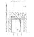
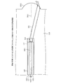
図1は、実施の形態1にかかる光導波路コネクタおよび光導波路の一例を示す正面断面図である。図1に示すように、実施の形態1にかかる光導波路コネクタ110は、たとえば、光導波路120と、光導波路140と、を接続する。一例としては、光導波路120は、LD(Laser Diode:レーザダイオード)やPD(Photo Diode:フォトダイオード)などの光素子に接続された光導波路である。また、光導波路140は、光伝送用の光導波路である。
(Embodiment 1)
(Optical Waveguide Connector and Optical Waveguide According to First Embodiment)
FIG. 1 is a front cross-sectional view illustrating an example of an optical waveguide connector and an optical waveguide according to the first embodiment. As shown in FIG. 1, the
光導波路120は、コア121と、クラッド122と、を含む。コア121は、クラッド122により囲まれている。また、コア121は、クラッド122より屈折率が高い。光導波路120へ入射された光101は、コア121の内部において、コア121とクラッド122との境界面で反射しながら伝播する。コア121の経は、一例としては50[μm]程度とすることができる。なお、光101は、一例としては変調された信号光である。
The
本実施の形態においては光導波路コネクタ110を介して光導波路120から光導波路140へ光101を伝播させる場合について説明するが、光導波路コネクタ110を介して光導波路140から光導波路120へ光を伝播させてもよい(たとえば図12参照)。
In this embodiment, a case where
光導波路コネクタ110は、光101を透過させる透明な部材によって形成される。たとえば、光導波路コネクタ110は、COP(Cyclo Olefin Polymer:シクロオレフィンポリマ)などの樹脂により、金型を用いて形成することができる。
The
また、光導波路コネクタ110は、スリット111を有する。スリット111は、光導波路120の端部を挿入するための挿入穴(接合部)である。スリット111において、光導波路120を挿入した際に光導波路120が突き当たる面(以下、「底面」と称する。)は、接着剤130を介して光導波路120の端面(図1における光導波路120の右側)と接着可能である。なお、図1に示す例では、光導波路コネクタ110は、端面だけでなく、端部の周囲(図1におけるスリット111の上下)も接着剤130を介してスリット111と接着されている。
The
光導波路120は、光導波路コネクタ110のスリット111に挿入され、接着剤130を介して光導波路コネクタ110に接続される。たとえば、スリット111に接着剤130を流し込み、スリット111に光導波路120の端部を挿入し、接着剤130を硬化させることで、図1に示すように、光導波路コネクタ110に光導波路120を接続することができる。接着剤130の硬化は、たとえば、熱や紫外線(UV)を接着剤130に照射することによって行うことができる。
The
また、光導波路コネクタ110のスリット111の底面(スリット111の図1における右側)であって、光導波路120の端面と対向する部分には、凹凸が形成されている。図1に示す例では、凹凸として凸部112および凹部113,114が形成されている。これにより、たとえばスリット111の底面に凹凸を設けない場合に比べて接着剤130と光導波路コネクタ110との間の接触面積を増やし、接着剤130と光導波路コネクタ110との間の接着強度を向上させることができる。なお、気泡151〜154は、スリット111に接着剤130を流し込んだ際に、凹部113,114において発生し得る気泡(空気だまり)である。
Further, unevenness is formed on the bottom surface of the
また、凸部112は、スリット111の底面における、光導波路120のコア121の端面に対向する部分に設けられている。これにより、凸部112は、光導波路120のコア121の端面から出射された光101を透過させることができる。凸部112を透過した光101は、光導波路コネクタ110の出射部(光導波路コネクタ110の図1における右側の端面)から光導波路コネクタ110の外部へ出射される。
Further, the
また、凸部112における光101の入射面は、コア121の端面より大きい。一例としては、凸部112の経は、コア121の経に対して+20%程度とすることができる。これにより、凸部112における光101の入射面が、光導波路120のコア121の端面から出射された光101の通過領域を包含するようにすることができる。このため、光導波路120のコア121の端面から出射された光101のうちの凸部112へ入射する光の割合を大きくし、光損失を抑制することができる。
Further, the incident surface of the
また、凹部113,114は、スリット111の底面における、光導波路120のクラッド122に対向する部分に設けられている。これにより、コア121の端面から出射される光101が、凸部112を通過して光導波路140へ入射され、凹部113,114は通過しないようにすることができる。このため、コア121から出射される光101の特性が、凹部113,114に発生し得る気泡151〜154によって劣化することを回避することができる。気泡151〜154による光101の劣化には、たとえばフレネル損による結合損失の低下がある。
Further, the
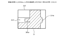
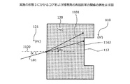
(実施の形態1にかかるレンズ付光導波路コネクタおよび光導波路)
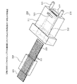
図2は、実施の形態1にかかるレンズ付光導波路コネクタおよび光導波路の一例を示す斜視図である。図2に示すレンズ付光導波路コネクタ210は、図1に示した光導波路コネクタ110に対応する構成である。図2に示す光導波路220は、図1に示した光導波路120に対応する構成である。すなわち、レンズ付光導波路コネクタ210は、光導波路220と、光導波路220と異なる光導波路と、を接続する。
(Optical Waveguide Connector with Lens and Optical Waveguide According to Embodiment 1)
FIG. 2 is a perspective view illustrating an example of an optical waveguide connector with a lens and an optical waveguide according to the first embodiment. The lens-attached
光導波路220は、コア群221と、クラッド222と、を含む。コア群221は、図1に示したコア121に対応する構成であって、アレイ上に設けられた複数のコアである。クラッド222は、図1に示したクラッド122に対応する構成であって、コア群221を囲むように形成されている。また、コア群221は、クラッド222より屈折率が高い。これにより、コア群221に含まれる各コアにおいて光を伝播させることができる。また、光導波路220には、光導波路220を挟むフェルールブーツ223が設けられている。
The
レンズ付光導波路コネクタ210は、コネクタ本体211と、スリット212と、空気穴213と、レンズアレイ214と、ピン215と、を有する。コネクタ本体211、スリット212、空気穴213、レンズアレイ214およびピン215は、たとえばCOPなどの透明な樹脂により、金型を用いて一体的に形成することができる。コネクタ本体211は、図1に示した光導波路コネクタ110の本体部に対応する構成であって、コア群221から出射された光を透過させてレンズアレイ214へ出射する。
The optical waveguide connector with
スリット212は、図1に示したスリット111に対応する構成であり、光導波路220を挿入するための挿入穴である。空気穴213は、スリット212の底面付近と、コネクタ本体211の表面と、をつなぐ穴である。空気穴213により、スリット212に接着剤を流し込んで光導波路220の端部を挿入する際に、スリット212の中にあった空気が外部へ抜け、大きな空気だまりの発生を低減することができる。
The
レンズアレイ214は、スリット212に挿入される光導波路220のコア群221の各コアに対応してアレイ状に設けられた複数のレンズである。レンズアレイ214に含まれる各レンズは、コア群221に含まれる各コアの端面から出射され、コネクタ本体211を透過した光を集光する。レンズアレイ214によって集光された各光は、レンズ付光導波路コネクタ210の外部(たとえば図1に示した光導波路140)へ出射される。
The
ピン215は、レンズ付光導波路コネクタ210を介して光導波路220と接続される光部品(たとえば図1に示した光導波路140)に対してコネクタ本体211を位置決めして固定するためのピンである。図1に示す例では2つのピン215が設けられている。
The
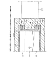
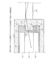
(実施の形態1にかかるレンズ付光導波路コネクタに光導波路を接続した状態)
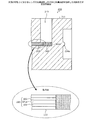
図3は、実施の形態1にかかるレンズ付光導波路コネクタに光導波路を接続した状態を示す正面断面図である。図3において、図2に示した部分と同様の部分については同一の符号を付して説明を省略する。接着剤302は、スリット212の底面と光導波路220の端面とを接着する接着剤である。
(A state where the optical waveguide is connected to the optical waveguide connector with a lens according to the first embodiment)
FIG. 3 is a front cross-sectional view illustrating a state in which an optical waveguide is connected to the optical waveguide connector with a lens according to the first embodiment. 3, parts that are the same as the parts shown in FIG. 2 are given the same reference numerals, and explanation thereof is omitted. The adhesive 302 is an adhesive that bonds the bottom surface of the
コア221aは、図2に示したコア群221に含まれる1個のコアである。レンズ214aは、図2に示したレンズアレイ214に含まれる1個のレンズである。コア221aを通過した光は、コア221aの端面から出射され、コネクタ本体211を通過し、レンズ214aによって集光されてレンズ付光導波路コネクタ210の外部へ出射される。
The core 221a is one core included in the
たとえば、スリット212の底面に液状の接着剤302を流し込み、スリット212の底面に光導波路220の端部を挿入し、接着剤302を硬化させることにより、スリット212の底面と光導波路220の端部とを接着することができる。接着剤302の流し込みは、光導波路220が挿入されるスリット212の開口部(スリット212の図2における左側)から行われてもよいし、空気穴213から行われてもよい。
For example, the
また、図1に示した光導波路コネクタ110と同様に、スリット212の底面は、凸部群(たとえば図4に示す凸部群301)が設けられることによって凹凸形状になっている。図3に示す凸部301aは、スリット212の底面に設けられた凸部群(たとえば図4参照)に含まれる1個の凸部である。これにより、接着剤302とコネクタ本体211との間の接触面積を増やし、接着剤302とコネクタ本体211との間の接着強度を向上させることができる。なお、スリット212の底面のうちの凸部(凸部301a)が設けられていない部分を凹部と称する。
Similarly to the
また、凸部301aは、スリット212の底面における、光導波路220のコア221aに対向する部分に設けられている。これにより、コア221aから出射される光が、凸部301aを通過し、スリット212の底面における凹部を通過しないようにすることができる。このため、コア221aから出射される光の特性が、接着剤302を流し込んだ際に凹部に発生し得る気泡によって劣化することを回避することができる。
Further, the
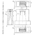
(実施の形態1にかかるレンズ付光導波路コネクタ)
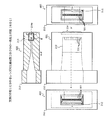
図4および図5は、実施の形態1にかかるレンズ付光導波路コネクタの一例を示す図である。図4,図5において、図2,図3に示した部分と同様の部分については同一の符号を付して説明を省略する。なお、図4においてはピン215の図示を省略している。
(Optical waveguide connector with a lens concerning Embodiment 1)
4 and 5 are diagrams illustrating an example of an optical waveguide connector with a lens according to the first embodiment. 4 and 5, the same parts as those shown in FIGS. 2 and 3 are denoted by the same reference numerals and description thereof is omitted. In addition, illustration of the
図4における平面図401および側面図402,403は、図2,図3に示したレンズ付光導波路コネクタ210の平面および両側面を示す。正面断面図404は、平面図401におけるA−A’断面を示す。図5においては、正面断面図404における領域Bを拡大して図示している。
A
図4,図5に示すように、スリット212の底面には、レンズアレイ214に含まれる各レンズに対応する各凸部からなる凸部群301が設けられている。凸部群301の各凸部の形状は、四角柱や円柱など各種の形状とすることができる。スリット212に挿入された光導波路220のコア群221から出射された各光は、それぞれ凸部群301の各凸部を通過して、それぞれレンズアレイ214に含まれる各レンズによって集光されて出射される。
As shown in FIGS. 4 and 5, the bottom surface of the
このように、実施の形態1にかかる光導波路コネクタによれば、光導波路の端部が挿入されるコネクタの挿入穴の底部に凹凸を設けることで、光導波路とコネクタを接着する接着剤と、コネクタと、の間の接触面積を大きくすることができる。このため、接着剤とコネクタとの間の接着強度の向上を図ることができる。 Thus, according to the optical waveguide connector according to the first embodiment, by providing irregularities at the bottom of the insertion hole of the connector into which the end of the optical waveguide is inserted, an adhesive that bonds the optical waveguide and the connector, The contact area between the connector and the connector can be increased. For this reason, the improvement of the adhesive strength between an adhesive agent and a connector can be aimed at.
たとえば、レンズ付光導波路コネクタ210のように光コネクタの本体とレンズを一体的に形成する場合等、光コネクタに使用できる材料に制限がある場合においても、コネクタの挿入穴の底部に凹凸を設けることで接着強度の向上を図ることができる。また、光導波路とコネクタの接着に汎用的な接着剤を用いても接着強度の向上を図ることができるため、設計の自由度を向上させることができる。
For example, even when the material that can be used for the optical connector is limited, such as when the optical connector body and the lens are integrally formed as in the optical waveguide connector with
また、光導波路のコアの端面に凸部が対向するように、すなわち光導波路のクラッドの端面に凹部が対向するように凹凸を設けることで、コアによって伝播する信号光が、凸部を通過し、凹部を通過しないようにすることができる。このため、凹部にできる接着剤の空泡による信号光の特性劣化を抑制することができる。 In addition, by providing concavity and convexity so that the convex portion faces the end surface of the core of the optical waveguide, that is, the concave portion faces the end surface of the clad of the optical waveguide, the signal light propagated by the core passes through the convex portion. , It can be prevented from passing through the recess. For this reason, the characteristic deterioration of the signal light by the bubble of the adhesive agent which can be made into a recessed part can be suppressed.
(実施の形態2)
実施の形態2について、実施の形態1と異なる部分について説明する。実施の形態2においては、光導波路のコアに対向する凸部に加えて光導波路のクラッドに対向する凸部を有する凹凸部を設ける構成について説明する。
(Embodiment 2)
In the second embodiment, parts different from the first embodiment will be described. In the second embodiment, a configuration is described in which a concavo-convex portion having a convex portion facing the cladding of the optical waveguide is provided in addition to the convex portion facing the core of the optical waveguide.
(実施の形態2にかかる光導波路コネクタおよび光導波路)
図6は、実施の形態2にかかる光導波路コネクタおよび光導波路の一例を示す正面断面図である。図6において、図1に示した部分と同様の部分については同一の符号を付して説明を省略する。図6に示すように、実施の形態2にかかる光導波路コネクタ110におけるスリット111の底面には、コア121に対向して設けられたスリット111に加えて、クラッド122に対向して設けられた凸部601,602が設けられている。これにより、接着剤130と光導波路コネクタ110との間の接触面積をさらに増やし、接着剤130と光導波路コネクタ110との間の接着強度を向上させることができる。
(Optical Waveguide Connector and Optical Waveguide According to Second Embodiment)
FIG. 6 is a front sectional view of an example of the optical waveguide connector and the optical waveguide according to the second embodiment. In FIG. 6, the same parts as those shown in FIG. As shown in FIG. 6, the bottom surface of the
また、凸部601,602を設けることにより、図1に示した気泡151〜154に加えて、凸部601,602の付近に気泡611〜614が発生し得る。しかし、光101はスリット111の凸部601,602の付近を通過しないため、光101の特性が気泡611〜614によって劣化することを回避することができる。
In addition to the
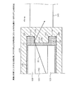
(実施の形態2にかかるレンズ付光導波路コネクタおよび光導波路)
図7および図8は、実施の形態2にかかるレンズ付光導波路コネクタおよび光導波路の一例を示す斜視図である。図7,図8において、図2〜図5に示した部分と同様の部分については同一の符号を付して説明を省略する。図8においては、図7の正面断面図404における領域Bを拡大して図示している。
(Optical Waveguide Connector with Lens and Optical Waveguide According to Second Embodiment)
7 and 8 are perspective views illustrating an example of an optical waveguide connector with a lens and an optical waveguide according to the second embodiment. 7 and FIG. 8, the same parts as those shown in FIG. 2 to FIG. In FIG. 8, the area B in the front
図7,図8に示すように、実施の形態2におけるスリット212の底面には、レンズアレイ214に含まれる各レンズに対応する凸部群301に加えて、凸部群301の各凸部とは異なる位置に設けられた凸部群701が設けられている。図7,図8に示す例では、凸部群301の凸部と、凸部群701の凸部と、が交互に並ぶように凸部群301および凸部群701が設けられている。
As shown in FIGS. 7 and 8, on the bottom surface of the
凸部群701の各凸部の形状は、凸部群301と同様に、四角柱や円柱など各種の形状とすることができる。また、図7,図8に示す例では、凸部群701の各凸部は、凸部群301の各凸部より経が小さくなるように形成されている。
The shape of each convex portion of the
実施の形態2にかかるレンズ付光導波路コネクタ210においても、スリット212に挿入された光導波路220のコア群221から出射された各光は、それぞれ凸部群301の各凸部を通過し、凸部群701の各凸部は通過しない。
Also in the optical waveguide connector with
図8に示す凸部701aは、図7に示した凸部群701に含まれる1個の凸部である。また、凸部701aは、スリット212の底面における、レンズアレイ214のレンズ(たとえばレンズ214a)と対向しない位置に設けられている。
A
このように、実施の形態2にかかる光導波路コネクタによれば、実施の形態1にかかる光導波路コネクタと同様に、信号光の特性劣化を抑制しつつ接着強度の向上を図ることができる。また、実施の形態2にかかる光導波路コネクタによれば、光導波路のコアに対向する凸部に加えて光導波路のクラッドに対向する凸部を有する凹凸部を設けることで、接着剤とコネクタとの間の接触面積を大きくすることができる。このため、接着剤とコネクタとの間の接着強度の向上を図ることができる。 As described above, according to the optical waveguide connector according to the second embodiment, as in the optical waveguide connector according to the first embodiment, it is possible to improve the adhesive strength while suppressing the characteristic deterioration of the signal light. Further, according to the optical waveguide connector according to the second embodiment, in addition to the convex portion facing the core of the optical waveguide, the concave and convex portion having the convex portion facing the cladding of the optical waveguide is provided. The contact area between the two can be increased. For this reason, the improvement of the adhesive strength between an adhesive agent and a connector can be aimed at.
(実施の形態3)
実施の形態3について、実施の形態1と異なる部分について説明する。実施の形態3においては、コネクタのスリット内の凸部を導波路として利用する構成について説明する。
(Embodiment 3)
The third embodiment will be described with respect to differences from the first embodiment. In the third embodiment, a configuration in which a convex portion in a slit of a connector is used as a waveguide will be described.
(実施の形態3にかかる光導波路コネクタおよび光導波路における光の伝播)
図9は、実施の形態3にかかる光導波路コネクタおよび光導波路における光の伝播の一例を示す正面断面図である。図9において、図1に示した部分と同様の部分については同一の符号を付して説明を省略する。図9に示すna,nc,nfは、それぞれ接着剤130、コア121および光導波路コネクタ110の屈折率である。
(Light Propagation in Optical Waveguide Connector and Optical Waveguide According to Embodiment 3)
FIG. 9 is a front sectional view illustrating an example of light propagation in the optical waveguide connector and the optical waveguide according to the third embodiment. In FIG. 9, the same parts as those shown in FIG. 9, na, nc, and nf are the refractive indexes of the adhesive 130, the
この場合に、nf>naとなるように、光導波路コネクタ110および接着剤130の材料を選定する。すなわち、接着剤130には、光導波路コネクタ110よりも屈折率が小さい接着剤を用いる。たとえば、光101の波長が850[nm]であり、上述したように光導波路コネクタ110にCOPを用いるとする。この場合は、一例としては、コア121の屈折率nc=1.56、接着剤130の屈折率na=1.50、光導波路コネクタ110の屈折率nf=1.51とすることができる。
In this case, the materials of the
これにより、コア121の端面から出射されて凸部112に入射した光101が、凸部112と接着剤130との間の境界面で反射しながら凸部112の内部を伝播するようにすることができる。このように、凸部112によって形成された凹凸を利用して光101の閉じ込め効率の向上を図ることができる。
Thereby, the light 101 emitted from the end face of the
(実施の形態3にかかる光導波路コネクタによる集光)
図10は、実施の形態3にかかる光導波路コネクタによる集光の一例を示す正面断面図である。図10において、図9に示した部分と同様の部分については同一の符号を付して説明を省略する。図10に示す例では、コア121の端面から出射され、凸部112を通過した光をレンズ1010によって集光して光導波路コネクタ110の外部へ出射する場合について説明する。この場合に、レンズ1010は、たとえば図2に示したレンズアレイ214に対応する構成である。
(Condensing light by the optical waveguide connector according to the third embodiment)
FIG. 10 is a front sectional view showing an example of light collection by the optical waveguide connector according to the third embodiment. In FIG. 10, the same parts as those shown in FIG. In the example shown in FIG. 10, a case where light emitted from the end face of the
レンズ中心1011は、レンズ1010の中心を示している。コア中心1001は、コア121の中心を示している。図10に示す例では、レンズ中心1011とコア中心1001との間にズレ1002(たとえば4[mm]程度)が生じている。ズレ1002は、たとえば光導波路120の位置がスリット111の内部でずれることによって発生する。
A
仮に、凸部112によって形成された凹凸を利用した光101の閉じ込めを行わない(たとえば凸部112を設けない)場合について説明する。この場合は、ズレ1002の発生により、コア121の端面から出射されて拡散する光101の広がり角度によっては、光101の一部がレンズ1010へ入射せずに光損失となる。
A case will be described in which light 101 is not confined using the unevenness formed by the convex portion 112 (for example, the
これに対して、凸部112によって形成された凹凸を利用した光101の閉じ込めを行うことで、図10に示すように、ズレ1002が生じていても、コア121の端面から出射されて拡散する光101をレンズ1010に集光させることができる。
On the other hand, by confining the light 101 using the unevenness formed by the
このように、凸部112によって形成された凹凸を導波路として利用することで、光101の閉じ込め効率の向上を図ることができる。このため、たとえばレンズ1010の小型化など、柔軟な設計が可能になる。
As described above, the confinement efficiency of the light 101 can be improved by using the unevenness formed by the
(実施の形態3にかかるコアおよび接着剤の各屈折率の関係の例)
図11は、実施の形態3にかかるコアおよび接着剤の各屈折率の関係の例を示す図である。図11において、図9,図10に示した部分と同様の部分については同一の符号を付して説明を省略する。θcは、コア121と接着剤130との境界面に対して垂直な基準方向1100と、コア121を伝播して接着剤130へ入射する光101の方向と、の間の角度(入射角)である。
(Example of relationship between refractive indexes of core and adhesive according to embodiment 3)
FIG. 11 is a diagram illustrating an example of the relationship between the refractive indexes of the core and the adhesive according to the third embodiment. In FIG. 11, the same parts as those shown in FIG. 9 and FIG. θc is an angle (incident angle) between the
光進行方向1101は、コア121の屈折率ncが、接着剤130の屈折率naより小さい場合(nc<na)において、コア121から接着剤130へ入射し、接着剤130を通過する光101の進行方向である。光進行方向1102は、コア121の屈折率ncが、接着剤130の屈折率naより大きい場合(nc>na)において、コア121から接着剤130へ入射し、接着剤130を通過する光101の進行方向である。
In the
光進行方向1101,1102に示すように、コア121の屈折率ncを接着剤130の屈折率naより大きく(nc>na)することで、接着剤130を通過する光101の方向と基準方向1100との間の角度θaを小さくすることができる。これにより、光導波路120と凸部112との間の位置ずれの許容範囲を広くすることができる。
As shown in the
したがって、接着剤130、コア121および光導波路コネクタ110の屈折率na,nc,nfは、一例としてはnc>nf>naとなるようにする。ただし、コア121の屈折率ncと、接着剤130および光導波路コネクタ110の屈折率na,nfと、の関係はこれに限らず、設計に応じて変更することができる。
Therefore, the refractive indexes na, nc, and nf of the adhesive 130, the
このように、実施の形態3にかかる光導波路コネクタによれば、実施の形態1にかかる光導波路コネクタと同様に、信号光の特性劣化を抑制しつつ接着強度の向上を図ることができる。また、実施の形態3にかかる光導波路コネクタによれば、コアに対向して設けられる凸部の屈折率を接着剤の屈折率より高くすることで、凸部と接着剤との境界面において反射させることにより凸部に光を透過させ、光損失を低減することができる。このため、信号光の特性劣化を抑制することができる。 As described above, according to the optical waveguide connector according to the third embodiment, as in the optical waveguide connector according to the first embodiment, it is possible to improve the adhesive strength while suppressing the characteristic deterioration of the signal light. In addition, according to the optical waveguide connector according to the third embodiment, the refractive index of the convex portion provided facing the core is made higher than the refractive index of the adhesive, thereby reflecting at the boundary surface between the convex portion and the adhesive. By doing so, light can be transmitted through the convex portion and light loss can be reduced. For this reason, the characteristic deterioration of the signal light can be suppressed.
なお、実施の形態3について実施の形態1と異なる部分について説明したが、実施の形態3において、たとえば実施の形態2のように、光導波路のコアに対向する凸部に加えて光導波路のクラッドに対向する凸部を有する凹凸部を設ける構成としてもよい。 Although the third embodiment is different from the first embodiment in the third embodiment, in the third embodiment, for example, as in the second embodiment, the clad of the optical waveguide in addition to the convex portion facing the core of the optical waveguide. It is good also as a structure which provides the uneven part which has a convex part which opposes.
(実施の形態4)
実施の形態4について、実施の形態1と異なる部分について説明する。上述した各実施の形態においては、光導波路120から光導波路コネクタ110へ光を伝播させる構成について説明したが、実施の形態3においては、光導波路コネクタ110から光導波路120へ光を伝播させる構成について説明する。
(Embodiment 4)
The fourth embodiment will be described with respect to differences from the first embodiment. In each of the embodiments described above, the configuration for propagating light from the
(実施の形態4にかかる光導波路コネクタおよび光導波路)
図12は、実施の形態4にかかる光導波路コネクタおよび光導波路の一例を示す正面断面図である。図12において、図1に示した部分と同様の部分については同一の符号を付して説明を省略する。図12に示すように、実施の形態4にかかる光導波路コネクタ110の入射部(光導波路コネクタ110の図12における右側の端面)には、光導波路140から出射された光1201が入射される。
(Optical Waveguide Connector and Optical Waveguide According to Embodiment 4)
FIG. 12 is a front sectional view of an example of the optical waveguide connector and the optical waveguide according to the fourth embodiment. In FIG. 12, the same parts as those shown in FIG. As shown in FIG. 12, the light 1201 emitted from the
光導波路コネクタ110へ入射された光1201は、凸部112および接着剤130を通過して、光導波路120のコア121の端面へ入射する。
The light 1201 incident on the
この場合に、凸部112における光1201の出射面(凸部112の図12における左側の端面)は、コア121の端面より小さい。一例としては、凸部112の経は、コア121の経に対して−20%程度とすることができる。これにより、光導波路120のコア121の端面が、凸部112から出射された光1201の通過領域を包含するようにすることができる。このため、凸部112から出射された光1201のうちの光導波路120のコア121の端面へ入射する光の割合を大きくし、光損失を抑制することができる。
In this case, the exit surface of the light 1201 in the convex portion 112 (the end surface on the left side in FIG. 12 of the convex portion 112) is smaller than the end surface of the
このように、実施の形態4にかかる光導波路コネクタによれば、光導波路コネクタ110から光導波路120へ光を伝播させる構成においても、実施の形態1にかかる光導波路コネクタと同様に、信号光の特性劣化を抑制しつつ接着強度の向上を図ることができる。
Thus, according to the optical waveguide connector according to the fourth embodiment, in the configuration in which light is propagated from the
なお、実施の形態4について実施の形態1と異なる部分について説明したが、実施の形態4において、たとえば実施の形態2のように、光導波路のコアに対向する凸部に加えて光導波路のクラッドに対向する凸部を有する凹凸部を設ける構成としてもよい。また、実施の形態4において、たとえば実施の形態3のように、コアに対向して設けられる凸部の屈折率を、接着剤の屈折率より高くする構成としてもよい。 Although the fourth embodiment is different from the first embodiment, in the fourth embodiment, for example, as in the second embodiment, the clad of the optical waveguide in addition to the convex portion facing the core of the optical waveguide. It is good also as a structure which provides the uneven part which has a convex part which opposes. Further, in the fourth embodiment, for example, as in the third embodiment, the refractive index of the convex portion provided facing the core may be higher than the refractive index of the adhesive.
以上説明したように、光導波路コネクタによれば、信号光の特性劣化を抑制しつつ接着強度の向上を図ることができる。 As described above, according to the optical waveguide connector, it is possible to improve the adhesive strength while suppressing the characteristic deterioration of the signal light.
たとえば、従来、レンズ付の光導波路コネクタは、耐熱耐湿、使用波長に対して透明等、使用できる材料に条件があり、材料が限られる場合がある。そのため、光導波路コネクタの材料に適した接着強度の高い接着剤が汎用品に少ない。また、レンズ付の光導波路コネクタに適した接着強度の高い専用の接着剤の開発には大きなコストがかかる。 For example, conventionally, an optical waveguide connector with a lens is limited in materials that can be used, such as heat and humidity resistance and transparent to the wavelength used, and the material may be limited. Therefore, there are few adhesives with high adhesive strength suitable for the material of the optical waveguide connector in general-purpose products. In addition, the development of a dedicated adhesive having high adhesive strength suitable for an optical waveguide connector with a lens requires a large cost.
これに対して、上述した各実施の形態によれば、接着剤で光導波路の端面と接着される、光導波路コネクタの挿入穴の底面に、光導波路のコアに凸部が対向するように凹凸を設ける構成とすることができる。これにより、接着剤と光導波路コネクタとの間の接着強度を高めつつ、凹部にできる接着剤の空泡による光の特性劣化を防ぐことができる。 On the other hand, according to each of the above-described embodiments, the bottom surface of the insertion hole of the optical waveguide connector that is bonded to the end surface of the optical waveguide with an adhesive so that the convex portion faces the core of the optical waveguide. It can be set as the structure which provides. Accordingly, it is possible to prevent the deterioration of the light characteristics due to the air bubbles of the adhesive that can be formed in the recess, while increasing the adhesive strength between the adhesive and the optical waveguide connector.
上述した各実施の形態に関し、さらに以下の付記を開示する。 The following additional notes are disclosed with respect to the above-described embodiments.
(付記1)光導波路の端部が挿入され、接着剤を介して光導波路の端面と接着可能な底面を有する挿入穴と、
前記挿入穴の前記底面に設けられ、前記挿入穴に挿入された前記光導波路のコアの端面に対向する位置に光を透過する凸部を有する凹凸部と、
を有することを特徴とする光導波路コネクタ。
(Supplementary Note 1) An insertion hole having a bottom surface into which an end portion of an optical waveguide is inserted and can be bonded to an end surface of the optical waveguide via an adhesive;
An uneven portion having a convex portion that is provided on the bottom surface of the insertion hole and transmits light at a position facing the end surface of the core of the optical waveguide inserted into the insertion hole;
An optical waveguide connector comprising:
(付記2)前記コアの端面から出射されて前記凸部を透過した光を出射し、
前記凸部は、前記コアの端面から出射された光が入射する入射面であって、前記コアの端面より大きい入射面を有する、
ことを特徴とする付記1に記載の光導波路コネクタ。
(Additional remark 2) The light radiate | emitted from the end surface of the said core and permeate | transmitted the said convex part is radiate | emitted,
The convex portion is an incident surface on which light emitted from an end surface of the core is incident, and has an incident surface larger than the end surface of the core.
The optical waveguide connector as set forth in Appendix 1, wherein
(付記3)入射されて前記凸部を透過した光を前記コアの端面へ出射し、
前記凸部は、前記凸部を透過した光を前記コアの端面へ出射する出射面であって、前記コアの端面より小さい出射面を有する、
ことを特徴とする付記1に記載の光導波路コネクタ。
(Appendix 3) Incident light transmitted through the convex portion is emitted to the end surface of the core,
The convex portion is an emission surface that emits light transmitted through the convex portion to an end surface of the core, and has an emission surface that is smaller than the end surface of the core.
The optical waveguide connector as set forth in Appendix 1, wherein
(付記4)前記凹凸部は、前記凸部と異なる凸部であって、前記挿入穴に挿入された前記光導波路のクラッドの端面に対向する位置に設けられた凸部を含むことを特徴とする付記1〜3のいずれか一つに記載の光導波路コネクタ。 (Additional remark 4) The said uneven part is a convex part different from the said convex part, Comprising: The convex part provided in the position facing the end surface of the clad of the said optical waveguide inserted in the said insertion hole is characterized by the above-mentioned. The optical waveguide connector according to any one of Supplementary notes 1 to 3.
(付記5)前記コアの端面に対向する位置に設けられた前記凸部の屈折率は、前記接着剤の屈折率より高いことを特徴とする付記1〜4のいずれか一つに記載の光導波路コネクタ。 (Additional remark 5) The refractive index of the said convex part provided in the position facing the end surface of the said core is higher than the refractive index of the said adhesive agent, The light guide as described in any one of Additional remark 1-4 characterized by the above-mentioned. Waveguide connector.
(付記6)前記コアの端面に対向する位置に設けられた前記凸部は、前記光を、前記接着剤との境界面において反射させることにより透過させることを特徴とする付記5に記載の光導波路コネクタ。 (Additional remark 6) The said convex part provided in the position facing the end surface of the said core permeate | transmits the said light by reflecting in the boundary surface with the said adhesive agent, The light guide of Additional remark 5 characterized by the above-mentioned. Waveguide connector.
(付記7)前記凹凸部と一体的に形成されたレンズを有し、
前記コアの端面から出射されて前記凸部を透過した光を前記レンズを介して出射し、または前記レンズを介して入射されて前記凸部を透過した光を前記コアの端面へ出射する、
ことを特徴とする付記1〜6のいずれか一つに記載の光導波路コネクタ。
(Additional remark 7) It has the lens formed integrally with the said uneven part,
The light emitted from the end surface of the core and transmitted through the convex portion is emitted through the lens, or the light incident through the lens and transmitted through the convex portion is emitted to the end surface of the core.
The optical waveguide connector according to any one of appendices 1 to 6, characterized in that:
110 光導波路コネクタ
111,212 スリット
112,301a,601,602,701a 凸部
113,114 凹部
120,140,220 光導波路
121,221a コア
122,222 クラッド
130,302 接着剤
151〜154,611〜614 気泡
210 レンズ付光導波路コネクタ
211 コネクタ本体
213 空気穴
214 レンズアレイ
214a,1010 レンズ
215 ピン
221 コア群
223 フェルールブーツ
301,701 凸部群
1001 コア中心
1002 ズレ
1011 レンズ中心
1100 基準方向
1101,1102 光進行方向
110 Optical waveguide connector 111,212 Slit 112,301a, 601,602,701a Convex part 113,114 Concave part 120,140,220 Optical waveguide 121,221a Core 122,222 Clad 130,302 Adhesive 151-154,611-614
Claims (4)
前記挿入穴の前記底面に設けられ、前記挿入穴に挿入された前記光導波路のコアの端面に対向する位置に光を透過する凸部を有する凹凸部と、
を有することを特徴とする光導波路コネクタ。 An insertion hole having a bottom surface into which the end of the optical waveguide is inserted and can be bonded to the end surface of the optical waveguide via an adhesive;
An uneven portion having a convex portion that is provided on the bottom surface of the insertion hole and transmits light at a position facing the end surface of the core of the optical waveguide inserted into the insertion hole;
An optical waveguide connector comprising:
前記コアの端面から出射されて前記凸部を透過した光を前記レンズを介して出射し、または前記レンズを介して入射されて前記凸部を透過した光を前記コアの端面へ出射する、
ことを特徴とする請求項1〜3のいずれか一つに記載の光導波路コネクタ。 It has a lens formed integrally with the uneven part,
The light emitted from the end surface of the core and transmitted through the convex portion is emitted through the lens, or the light incident through the lens and transmitted through the convex portion is emitted to the end surface of the core.
The optical waveguide connector according to any one of claims 1 to 3, wherein
Priority Applications (2)
| Application Number | Priority Date | Filing Date | Title |
|---|---|---|---|
| JP2015164104A JP2017040887A (en) | 2015-08-21 | 2015-08-21 | Optical waveguide connector |
| US15/236,916 US10139566B2 (en) | 2015-08-21 | 2016-08-15 | Optical waveguide connector |
Applications Claiming Priority (1)
| Application Number | Priority Date | Filing Date | Title |
|---|---|---|---|
| JP2015164104A JP2017040887A (en) | 2015-08-21 | 2015-08-21 | Optical waveguide connector |
Publications (1)
| Publication Number | Publication Date |
|---|---|
| JP2017040887A true JP2017040887A (en) | 2017-02-23 |
Family
ID=58158446
Family Applications (1)
| Application Number | Title | Priority Date | Filing Date |
|---|---|---|---|
| JP2015164104A Pending JP2017040887A (en) | 2015-08-21 | 2015-08-21 | Optical waveguide connector |
Country Status (2)
| Country | Link |
|---|---|
| US (1) | US10139566B2 (en) |
| JP (1) | JP2017040887A (en) |
Cited By (1)
| Publication number | Priority date | Publication date | Assignee | Title |
|---|---|---|---|---|
| JP6401888B1 (en) * | 2017-06-16 | 2018-10-10 | 京セラ株式会社 | Optical connector module |
Families Citing this family (3)
| Publication number | Priority date | Publication date | Assignee | Title |
|---|---|---|---|---|
| WO2019207976A1 (en) * | 2018-04-26 | 2019-10-31 | ソニー株式会社 | Optical communication connector, optical transmitter, optical receiver, optical communication system, and optical communication cable |
| JP2020020930A (en) * | 2018-07-31 | 2020-02-06 | 富士通コンポーネント株式会社 | Optical module |
| JP7449808B2 (en) * | 2020-07-29 | 2024-03-14 | 京セラ株式会社 | Optical connectors and optical connector modules |
Citations (3)
| Publication number | Priority date | Publication date | Assignee | Title |
|---|---|---|---|---|
| US20120106896A1 (en) * | 2010-10-29 | 2012-05-03 | Hon Hai Precision Industry Co., Ltd. | Cable assembly for optical termination |
| JP2013020027A (en) * | 2011-07-08 | 2013-01-31 | Fujitsu Ltd | Optical transmission line and method of manufacturing the same |
| JP2014010186A (en) * | 2012-06-27 | 2014-01-20 | Fujifilm Corp | Optical connector |
Family Cites Families (6)
| Publication number | Priority date | Publication date | Assignee | Title |
|---|---|---|---|---|
| JP2003329877A (en) | 2002-05-14 | 2003-11-19 | Nippon Sheet Glass Co Ltd | Optical module |
| JP4115894B2 (en) | 2003-07-01 | 2008-07-09 | 株式会社リコー | Compound optical device |
| JP4095522B2 (en) | 2003-09-22 | 2008-06-04 | 株式会社リコー | Method for manufacturing composite optical device |
| JP2005284015A (en) * | 2004-03-30 | 2005-10-13 | Mitsubishi Electric Corp | Optical module and optical fiber used therefor |
| US20120068368A1 (en) * | 2009-06-03 | 2012-03-22 | Panasonic Corporation | Method for manufacturing optical diffraction element |
| US9201201B2 (en) * | 2012-04-20 | 2015-12-01 | Corning Cable Systems Llc | Fiber trays, fiber optical modules, and methods of processing optical fibers |
-
2015
- 2015-08-21 JP JP2015164104A patent/JP2017040887A/en active Pending
-
2016
- 2016-08-15 US US15/236,916 patent/US10139566B2/en not_active Expired - Fee Related
Patent Citations (3)
| Publication number | Priority date | Publication date | Assignee | Title |
|---|---|---|---|---|
| US20120106896A1 (en) * | 2010-10-29 | 2012-05-03 | Hon Hai Precision Industry Co., Ltd. | Cable assembly for optical termination |
| JP2013020027A (en) * | 2011-07-08 | 2013-01-31 | Fujitsu Ltd | Optical transmission line and method of manufacturing the same |
| JP2014010186A (en) * | 2012-06-27 | 2014-01-20 | Fujifilm Corp | Optical connector |
Cited By (2)
| Publication number | Priority date | Publication date | Assignee | Title |
|---|---|---|---|---|
| JP6401888B1 (en) * | 2017-06-16 | 2018-10-10 | 京セラ株式会社 | Optical connector module |
| WO2018229992A1 (en) * | 2017-06-16 | 2018-12-20 | 京セラ株式会社 | Optical connector module |
Also Published As
| Publication number | Publication date |
|---|---|
| US20170052320A1 (en) | 2017-02-23 |
| US10139566B2 (en) | 2018-11-27 |
Similar Documents
| Publication | Publication Date | Title |
|---|---|---|
| CN110741295B (en) | Optical connector module | |
| TWI612353B (en) | Optical socket and optical module having the same | |
| JP6644080B2 (en) | Optical connector, optical connector system, and active optical cable having the same | |
| JP4903120B2 (en) | Optical path changing member | |
| JP5328533B2 (en) | Optical connector | |
| JP2019152804A (en) | Optical connector | |
| JP2013200347A (en) | Optical receptacle and optical module including the same | |
| JP6359848B2 (en) | Optical receptacle and optical module having the same | |
| US10139566B2 (en) | Optical waveguide connector | |
| TW201307933A (en) | Optical module | |
| US20190219777A1 (en) | Optical connection structure | |
| JP6979381B2 (en) | Optical connector module | |
| CN107430246B (en) | Optical transmission module | |
| US20210302672A1 (en) | Optical receptacle and optical module | |
| CN116134353A (en) | Optical connector and optical connector module | |
| WO2013136925A1 (en) | Optical receptacle and optical module provided with same | |
| JP5920813B2 (en) | Optical module | |
| WO2025244025A1 (en) | Optical module | |
| JP2005164665A (en) | Light emitting module | |
| JP2006011279A (en) | Optical fiber collimator | |
| JP2009025483A (en) | Optical waveguide array, optical device and optical connector | |
| JP2005338297A (en) | Optical coupling lens and optical communication device |
Legal Events
| Date | Code | Title | Description |
|---|---|---|---|
| A621 | Written request for application examination |
Free format text: JAPANESE INTERMEDIATE CODE: A621 Effective date: 20180514 |
|
| A131 | Notification of reasons for refusal |
Free format text: JAPANESE INTERMEDIATE CODE: A131 Effective date: 20190122 |
|
| A977 | Report on retrieval |
Free format text: JAPANESE INTERMEDIATE CODE: A971007 Effective date: 20190123 |
|
| A521 | Request for written amendment filed |
Free format text: JAPANESE INTERMEDIATE CODE: A523 Effective date: 20190314 |
|
| A02 | Decision of refusal |
Free format text: JAPANESE INTERMEDIATE CODE: A02 Effective date: 20190813 |