JP2017017110A - Semiconductor light emitting element emitting deep ultraviolet light, light emitting module including semiconductor light emitting element, and manufacturing method of semiconductor light emitting element - Google Patents

Semiconductor light emitting element emitting deep ultraviolet light, light emitting module including semiconductor light emitting element, and manufacturing method of semiconductor light emitting element Download PDF

Info

Publication number
JP2017017110A
JP2017017110A JP2015130266A JP2015130266A JP2017017110A JP 2017017110 A JP2017017110 A JP 2017017110A JP 2015130266 A JP2015130266 A JP 2015130266A JP 2015130266 A JP2015130266 A JP 2015130266A JP 2017017110 A JP2017017110 A JP 2017017110A
Authority
JP
Japan
Prior art keywords
light emitting
semiconductor light
substrate
emitting element
main surface
Prior art date
Legal status (The legal status is an assumption and is not a legal conclusion. Google has not performed a legal analysis and makes no representation as to the accuracy of the status listed.)
Granted
Application number
JP2015130266A
Other languages
Japanese (ja)
Other versions
JP6521443B2 (en
Inventor
井上 振一郎
Shinichiro Inoue
振一郎 井上
学 谷口
Manabu Taniguchi
学 谷口
Current Assignee (The listed assignees may be inaccurate. Google has not performed a legal analysis and makes no representation or warranty as to the accuracy of the list.)
National Institute of Information and Communications Technology
Original Assignee
National Institute of Information and Communications Technology
Priority date (The priority date is an assumption and is not a legal conclusion. Google has not performed a legal analysis and makes no representation as to the accuracy of the date listed.)
Filing date
Publication date
Application filed by National Institute of Information and Communications Technology filed Critical National Institute of Information and Communications Technology
Priority to JP2015130266A priority Critical patent/JP6521443B2/en
Publication of JP2017017110A publication Critical patent/JP2017017110A/en
Application granted granted Critical
Publication of JP6521443B2 publication Critical patent/JP6521443B2/en
Active legal-status Critical Current
Anticipated expiration legal-status Critical

Links

Images

Abstract

PROBLEM TO BE SOLVED: To provide a semiconductor light emitting element having improved light extraction efficiency and emitting deep ultraviolet light.SOLUTION: A semiconductor light emitting element 1 emitting deep ultraviolet light includes: a substrate 11 having a first main surface 11a, a second main surface 11b on an opposite side of the first main surface 11a, and a side surface 11c extending between the first main surface 11a and the second main surface 11b; and an active layer 13 provided on the first main surface 11a of the substrate 11. The supplementary angle θ formed between the first main surface 11a of the substrate 11 and at least a part of the side surface 11c of the substrate 11 is 20° or above and 70° or below, or 100° or above and 140° or below. The optical absorption coefficient α(cm) of the substrate 11 and the thickness t (μm) of the substrate 11 satisfy 340exp(-0.16α)≤t≤3,200α.SELECTED DRAWING: Figure 1

Description

本発明は、深紫外光を放射する半導体発光素子、該半導体発光素子を備える発光モジュール、及び該半導体発光素子の製造方法に関する。   The present invention relates to a semiconductor light emitting device that emits deep ultraviolet light, a light emitting module including the semiconductor light emitting device, and a method for manufacturing the semiconductor light emitting device.

従来、深紫外光を放射する半導体発光素子が知られている(非特許文献1)。また、可視または赤外の光を放射する半導体発光素子では、半導体発光素子の光取り出し効率を向上させるために、半導体発光素子の基板の側面を傾斜させることが知られている(非特許文献2、非特許文献3)。   Conventionally, a semiconductor light emitting element that emits deep ultraviolet light is known (Non-Patent Document 1). Further, in a semiconductor light emitting device that emits visible or infrared light, it is known that the side surface of the substrate of the semiconductor light emitting device is inclined in order to improve the light extraction efficiency of the semiconductor light emitting device (Non-patent Document 2). Non-Patent Document 3).

James R. Grandusky、外8名、「270 nm Pseudomorphic Ultraviolet Light-Emitting Diodes with Over 60 mW Continuous Wave Output Power」、Applied Physics Express、2013年2月26日、第6巻、p.032101James R. Grandusky, 8 others, "270 nm Pseudomorphic Ultraviolet Light-Emitting Diodes with Over 60 mW Continuous Wave Output Power", Applied Physics Express, February 26, 2013, Volume 6, p.032101 M. R. Krames、外12名、「High-power truncated-inverted-pyramid (AlxGa1-x)0.5In0.5P/GaP light-emitting diodes exhibiting >50% external quantum efficiency」、Applied Physics Letters、1999年10月18日、第75巻、第16号、p.2365−2367MR Krames, 12 others, `` High-power truncated-inverted-pyramid (AlxGa1-x) 0.5In0.5P / GaP light-emitting diodes exhibiting> 50% external quantum efficiency '', Applied Physics Letters, October 18, 1999 75, No. 16, p.2365-2367 U. Strauss、外8名、「Progress of InGaN Light Emitting Diodes on SiC」、Physica Status Solidi (c)、2002年、第0巻、第1号 p.276−279U. Strauss, 8 others, `` Progress of InGaN Light Emitting Diodes on SiC '', Physica Status Solidi (c), 2002, Volume 0, No. 1, p.276-279

半導体発光素子の基板は、可視及び赤外の光よりも、格段に多くの深紫外光を吸収する。そのため、非特許文献1に記載された深紫外光を放射する半導体発光素子では、深紫外光の取り出し効率を高めるために、基板をできる限り薄くしている。しかし、非特許文献1に記載の深紫外光を放射する半導体発光素子は、依然として、深紫外光の取り出し効率が低い。他方、非特許文献2及び3に記載された可視及び赤外の光を放射する半導体発光素子では、可視及び赤外の光が基板で吸収されることを無視し得る。そのため、可視及び赤外の光を放射する半導体発光素子では、半導体発光素子から放射された光が基板で吸収されることが全く考慮されておらず、厚い基板が用いられている。これに対し、半導体発光素子の基板は、可視及び赤外の光よりも、格段に多くの深紫外光を吸収する。そのため、可視及び赤外の光を放射する半導体発光素子に用いられていた技術を、深紫外光を放射する半導体発光素子にそのまま適用すると、多くの深紫外光が基板で吸収されてしまい、深紫外光を放射する半導体発光素子の光取り出し効率を十分に向上させることができないことが、我々の検討の結果明らかになった。   The substrate of the semiconductor light emitting device absorbs much more deep ultraviolet light than visible and infrared light. Therefore, in the semiconductor light emitting device that emits deep ultraviolet light described in Non-Patent Document 1, the substrate is made as thin as possible in order to increase the extraction efficiency of deep ultraviolet light. However, the semiconductor light emitting device that emits deep ultraviolet light described in Non-Patent Document 1 still has a low extraction efficiency of deep ultraviolet light. On the other hand, in the semiconductor light emitting device that emits visible and infrared light described in Non-Patent Documents 2 and 3, it can be ignored that the visible and infrared light is absorbed by the substrate. Therefore, in a semiconductor light emitting device that emits visible and infrared light, it is not considered at all that the light emitted from the semiconductor light emitting device is absorbed by the substrate, and a thick substrate is used. On the other hand, the substrate of the semiconductor light emitting device absorbs much more deep ultraviolet light than visible and infrared light. Therefore, if the technology used in the semiconductor light emitting device that emits visible and infrared light is directly applied to the semiconductor light emitting device that emits deep ultraviolet light, a lot of deep ultraviolet light is absorbed by the substrate. As a result of our examination, it has become clear that the light extraction efficiency of a semiconductor light emitting device emitting ultraviolet light cannot be sufficiently improved.

本発明は、上記の課題を鑑みてなされたものであり、その目的は、向上した光取り出し効率を有する、深紫外光を放射する半導体発光素子及びその製造方法を提供することである。   The present invention has been made in view of the above problems, and an object of the present invention is to provide a semiconductor light emitting device that emits deep ultraviolet light and has an improved light extraction efficiency, and a method for manufacturing the same.

本発明の別の目的は、向上した光取り出し効率を有する、深紫外光を放射する半導体発光素子を備える発光モジュールを提供することである。   Another object of the present invention is to provide a light emitting module comprising a semiconductor light emitting element that emits deep ultraviolet light and has improved light extraction efficiency.

本発明の深紫外光を放射する半導体発光素子は、第1の主面と、第1の主面と反対側の第2の主面と、第1の主面と第2の主面との間に延在する側面とを有する基板と、基板の第1の主面上に設けられた活性層とを備え、基板の第1の主面と少なくとも一部の側面とがなす角の補角θは、20°以上70°以下、または、100°以上140°以下であり、基板の光吸収係数α(cm-1)及び基板の厚さt(μm)は、340exp(−0.16α)≦t≦3200α-0.7を満たす。 The semiconductor light emitting device that emits deep ultraviolet light according to the present invention includes a first main surface, a second main surface opposite to the first main surface, a first main surface, and a second main surface. Complementing an angle formed by a substrate having a side surface extending in between and an active layer provided on the first main surface of the substrate, and formed by the first main surface of the substrate and at least a part of the side surfaces θ is 20 ° or more and 70 ° or less, or 100 ° or more and 140 ° or less, and the light absorption coefficient α (cm −1 ) of the substrate and the thickness t (μm) of the substrate are 340 exp (−0.16α). <= T <= 3200 (alpha) -0.7 is satisfy | filled.

本発明の深紫外光を放射する半導体発光素子の製造方法は、第1の主面と、第1の主面と反対側の第2の主面とを有するウエハの光吸収係数α(cm-1)を求めることと、ウエハの第1の主面上に活性層を形成することと、ウエハの光吸収係数α(cm-1)及びウエハの厚さt(μm)が、340exp(−0.16α)≦t≦3200α-0.7を満たすように、ウエハの厚さtを定めることと、ウエハを、複数の基板に分割することとを備える。複数の基板のそれぞれは、活性層が形成された第1の主面と、第1の主面と反対側の第2の主面と、第1の主面と第2の主面との間に延在する側面とを有する。本発明の深紫外光を放射する半導体発光素子の製造方法は、さらに、基板の第1の主面と基板の少なくとも一部の側面とがなす角の補角が、20°以上70°以下、または、100°以上140°以下になるように、基板の少なくとも一部の側面を加工することを備える。 The method for manufacturing a semiconductor light emitting device that emits deep ultraviolet light according to the present invention includes a light absorption coefficient α (cm of a wafer having a first main surface and a second main surface opposite to the first main surface. 1 ), an active layer is formed on the first main surface of the wafer, the light absorption coefficient α (cm −1 ) of the wafer and the thickness t (μm) of the wafer are 340 exp (−0 .16α) ≦ t ≦ 3200α− 0.7 , and determining the wafer thickness t, and dividing the wafer into a plurality of substrates. Each of the plurality of substrates includes a first main surface on which an active layer is formed, a second main surface opposite to the first main surface, and between the first main surface and the second main surface. And a side surface extending to the surface. In the method for manufacturing a semiconductor light emitting device that emits deep ultraviolet light according to the present invention, the complementary angle of the angle formed by the first main surface of the substrate and at least a part of the side surface of the substrate is 20 ° or more and 70 ° or less, Alternatively, at least a part of the side surface of the substrate is processed so as to be 100 ° to 140 °.

本発明の発光モジュールは、上記のような半導体発光素子と、半導体発光素子を支持する支持部材と、半導体発光素子を収容するパッケージとを備える。パッケージは、半導体発光素子から放射される光に対して透明な透明部材を有する。   The light emitting module of the present invention includes the semiconductor light emitting element as described above, a support member that supports the semiconductor light emitting element, and a package that houses the semiconductor light emitting element. The package has a transparent member that is transparent to light emitted from the semiconductor light emitting device.

本発明の半導体発光素子によれば、向上した光取り出し効率を有する、深紫外光を放射する半導体発光素子を提供することができる。   According to the semiconductor light emitting device of the present invention, it is possible to provide a semiconductor light emitting device that emits deep ultraviolet light and has improved light extraction efficiency.

本発明の半導体発光素子の製造方法によれば、向上した光取り出し効率を有する、深紫外光を放射する半導体発光素子を製造する方法を提供することができる。   According to the method for manufacturing a semiconductor light emitting device of the present invention, it is possible to provide a method for manufacturing a semiconductor light emitting device that emits deep ultraviolet light and has improved light extraction efficiency.

本発明の発光モジュールによれば、向上した光取り出し効率を有する、深紫外光を放射する半導体発光素子を備える発光モジュールを提供することができる。   According to the light emitting module of the present invention, it is possible to provide a light emitting module including a semiconductor light emitting element that emits deep ultraviolet light and has improved light extraction efficiency.

実施の形態1に係る半導体発光素子(θ<90°)の概略断面図である。2 is a schematic cross-sectional view of the semiconductor light emitting element (θ <90 °) according to Embodiment 1. FIG. 実施の形態1に係る半導体発光素子(θ>90°)の概略断面図である。1 is a schematic cross-sectional view of a semiconductor light emitting element (θ> 90 °) according to Embodiment 1. FIG. 実施の形態1に係る半導体発光素子の基板が、窒化アルミニウムで形成されるとともに、1cm-1の光吸収係数α、2.29の屈折率n及び800μmの幅wを有する場合の、基板の厚さt及び補角θに対する半導体発光素子(θ<90°)の規格化光取り出し効率のシミュレーション結果を示す図である。The thickness of the substrate when the substrate of the semiconductor light emitting device according to the first embodiment is made of aluminum nitride and has a light absorption coefficient α of 1 cm −1 , a refractive index n of 2.29, and a width w of 800 μm. It is a figure which shows the simulation result of the normalized light extraction efficiency of the semiconductor light-emitting device (θ <90 °) with respect to the length t and the complementary angle θ. 実施の形態1に係る半導体発光素子の基板が、窒化アルミニウムで形成されるとともに、1cm-1の光吸収係数α、2.29の屈折率n及び800μmの幅wを有する場合の、基板の厚さt及び補角θに対する半導体発光素子(θ>90°)の規格化光取り出し効率のシミュレーション結果を示す図である。The thickness of the substrate when the substrate of the semiconductor light emitting device according to the first embodiment is made of aluminum nitride and has a light absorption coefficient α of 1 cm −1 , a refractive index n of 2.29, and a width w of 800 μm. It is a figure which shows the simulation result of the normalization light extraction efficiency of the semiconductor light-emitting device ((theta)> 90 degrees) with respect to length t and complementary angle (theta). 実施の形態1に係る半導体発光素子の基板が、窒化アルミニウムで形成されるとともに、3cm-1の光吸収係数α、2.29の屈折率n及び800μmの幅wを有する場合の、基板の厚さt及び補角θに対する半導体発光素子(θ<90°)の規格化光取り出し効率のシミュレーション結果を示す図である。The thickness of the substrate when the substrate of the semiconductor light emitting device according to the first embodiment is made of aluminum nitride and has a light absorption coefficient α of 3 cm −1 , a refractive index n of 2.29, and a width w of 800 μm. It is a figure which shows the simulation result of the normalized light extraction efficiency of the semiconductor light-emitting device (θ <90 °) with respect to the length t and the complementary angle θ. 実施の形態1に係る半導体発光素子の基板が、窒化アルミニウムで形成されるとともに、3cm-1の光吸収係数α、2.29の屈折率n及び800μmの幅wを有する場合の、基板の厚さt及び補角θに対する半導体発光素子(θ>90°)の規格化光取り出し効率のシミュレーション結果を示す図である。The thickness of the substrate when the substrate of the semiconductor light emitting device according to the first embodiment is made of aluminum nitride and has a light absorption coefficient α of 3 cm −1 , a refractive index n of 2.29, and a width w of 800 μm. It is a figure which shows the simulation result of the normalization light extraction efficiency of the semiconductor light-emitting device ((theta)> 90 degrees) with respect to length t and complementary angle (theta). 実施の形態1に係る半導体発光素子の基板が、窒化アルミニウムで形成されるとともに、9cm-1の光吸収係数α、2.29の屈折率n及び800μmの幅wを有する場合の、基板の厚さt及び補角θに対する半導体発光素子(θ<90°)の規格化光取り出し効率のシミュレーション結果を示す図である。The thickness of the substrate in the case where the substrate of the semiconductor light emitting element according to the first embodiment is made of aluminum nitride and has a light absorption coefficient α of 9 cm −1 , a refractive index n of 2.29 and a width w of 800 μm. It is a figure which shows the simulation result of the normalized light extraction efficiency of the semiconductor light-emitting device (θ <90 °) with respect to the length t and the complementary angle θ. 実施の形態1に係る半導体発光素子の基板が、窒化アルミニウムで形成されるとともに、9cm-1の光吸収係数α、2.29の屈折率n及び800μmの幅wを有する場合の、基板の厚さt及び補角θに対する半導体発光素子(θ>90°)の規格化光取り出し効率のシミュレーション結果を示す図である。The thickness of the substrate in the case where the substrate of the semiconductor light emitting element according to the first embodiment is made of aluminum nitride and has a light absorption coefficient α of 9 cm −1 , a refractive index n of 2.29 and a width w of 800 μm. It is a figure which shows the simulation result of the normalization light extraction efficiency of the semiconductor light-emitting device ((theta)> 90 degrees) with respect to length t and complementary angle (theta). 実施の形態1に係る半導体発光素子の基板が、窒化アルミニウムで形成されるとともに、20cm-1の光吸収係数α、2.29の屈折率n及び800μmの幅wを有する場合の、基板の厚さt及び補角θに対する半導体発光素子(θ<90°)の規格化光取り出し効率のシミュレーション結果を示す図である。The thickness of the substrate when the substrate of the semiconductor light emitting device according to the first embodiment is made of aluminum nitride and has a light absorption coefficient α of 20 cm −1 , a refractive index n of 2.29, and a width w of 800 μm. It is a figure which shows the simulation result of the normalized light extraction efficiency of the semiconductor light-emitting device (θ <90 °) with respect to the length t and the complementary angle θ. 実施の形態1に係る半導体発光素子の基板が、窒化アルミニウムで形成されるとともに、20cm-1の光吸収係数α、2.29の屈折率n及び800μmの幅wを有する場合の、基板の厚さt及び補角θに対する半導体発光素子(θ>90°)の規格化光取り出し効率のシミュレーション結果を示す図である。The thickness of the substrate when the substrate of the semiconductor light emitting device according to the first embodiment is made of aluminum nitride and has a light absorption coefficient α of 20 cm −1 , a refractive index n of 2.29, and a width w of 800 μm. It is a figure which shows the simulation result of the normalization light extraction efficiency of the semiconductor light-emitting device ((theta)> 90 degrees) with respect to length t and complementary angle (theta). 実施の形態1に係る半導体発光素子の基板が、窒化アルミニウムで形成されるとともに、30cm-1の光吸収係数α、2.29の屈折率n及び800μmの幅wを有する場合の、基板の厚さt及び補角θに対する半導体発光素子(θ<90°)の規格化光取り出し効率のシミュレーション結果を示す図である。The thickness of the substrate in the case where the substrate of the semiconductor light emitting element according to Embodiment 1 is formed of aluminum nitride and has a light absorption coefficient α of 30 cm −1 , a refractive index n of 2.29, and a width w of 800 μm. It is a figure which shows the simulation result of the normalized light extraction efficiency of the semiconductor light-emitting device (θ <90 °) with respect to the length t and the complementary angle θ. 実施の形態1に係る半導体発光素子の基板が、窒化アルミニウムで形成されるとともに、30cm-1の光吸収係数α、2.29の屈折率n及び800μmの幅wを有する場合の、基板の厚さt及び補角θに対する半導体発光素子(θ>90°)の規格化光取り出し効率のシミュレーション結果を示す図である。The thickness of the substrate in the case where the substrate of the semiconductor light emitting element according to Embodiment 1 is formed of aluminum nitride and has a light absorption coefficient α of 30 cm −1 , a refractive index n of 2.29, and a width w of 800 μm. It is a figure which shows the simulation result of the normalization light extraction efficiency of the semiconductor light-emitting device ((theta)> 90 degrees) with respect to length t and complementary angle (theta). 実施の形態1に係る半導体発光素子の基板が、窒化アルミニウムで形成されるとともに、40cm-1の光吸収係数α、2.29の屈折率n及び800μmの幅wを有する場合の、基板の厚さt及び補角θに対する半導体発光素子(θ<90°)の規格化光取り出し効率のシミュレーション結果を示す図である。The thickness of the substrate when the substrate of the semiconductor light emitting device according to the first embodiment is made of aluminum nitride and has a light absorption coefficient α of 40 cm −1 , a refractive index n of 2.29, and a width w of 800 μm. It is a figure which shows the simulation result of the normalized light extraction efficiency of the semiconductor light-emitting device (θ <90 °) with respect to the length t and the complementary angle θ. 実施の形態1に係る半導体発光素子の基板が、窒化アルミニウムで形成されるとともに、40cm-1の光吸収係数α、2.29の屈折率n及び800μmの幅wを有する場合の、基板の厚さt及び補角θに対する半導体発光素子(θ>90°)の規格化光取り出し効率のシミュレーション結果を示す図である。The thickness of the substrate when the substrate of the semiconductor light emitting device according to the first embodiment is made of aluminum nitride and has a light absorption coefficient α of 40 cm −1 , a refractive index n of 2.29, and a width w of 800 μm. It is a figure which shows the simulation result of the normalization light extraction efficiency of the semiconductor light-emitting device ((theta)> 90 degrees) with respect to length t and complementary angle (theta). 実施の形態1に係る半導体発光素子の基板が、窒化アルミニウムで形成されるとともに、5.6cm-1の光吸収係数α、2.18の屈折率n及び800μmの幅wを有する場合の、基板の厚さt及び補角θに対する半導体発光素子(θ<90°)の規格化光取り出し効率のシミュレーション結果を示す図である。The substrate in the case where the substrate of the semiconductor light emitting element according to the first embodiment is formed of aluminum nitride and has a light absorption coefficient α of 5.6 cm −1 , a refractive index n of 2.18 and a width w of 800 μm. It is a figure which shows the simulation result of the normalization light extraction efficiency of the semiconductor light-emitting device ((theta) <90 degrees) with respect to thickness t and complementary angle (theta). 実施の形態1に係る半導体発光素子の基板が、窒化アルミニウムで形成されるとともに、5.6cm-1の光吸収係数α、2.18の屈折率n及び800μmの幅wを有する場合の、基板の厚さt及び補角θに対する半導体発光素子(θ>90°)の規格化光取り出し効率のシミュレーション結果を示す図である。The substrate in the case where the substrate of the semiconductor light emitting element according to the first embodiment is formed of aluminum nitride and has a light absorption coefficient α of 5.6 cm −1 , a refractive index n of 2.18 and a width w of 800 μm. It is a figure which shows the simulation result of the normalized light extraction efficiency of the semiconductor light-emitting device ((theta)> 90 degrees) with respect to the thickness t and complementary angle (theta) of FIG. 実施の形態1に係る半導体発光素子の基板が窒化アルミニウムで形成される場合の、光吸収係数αと基板の厚さtとの関係のシミュレーション結果を示す図である。It is a figure which shows the simulation result of the relationship between the light absorption coefficient (alpha) and the thickness t of a board | substrate in case the board | substrate of the semiconductor light-emitting device concerning Embodiment 1 is formed with aluminum nitride. (A)は、実施の形態1に係る半導体発光素子(θ<90°)の基板の第1の主面の中央部の発光点から放射される光線を示す図である。(B)は、実施の形態1に係る半導体発光素子(θ>90°)の基板の第1の主面の中央部の発光点から放射される光線を示す図である。(A) is a figure which shows the light ray radiated | emitted from the light emission point of the center part of the 1st main surface of the board | substrate of the semiconductor light-emitting device ((theta) <90 degrees) which concerns on Embodiment 1. FIG. (B) is a figure which shows the light ray radiated | emitted from the light emission point of the center part of the 1st main surface of the board | substrate of the semiconductor light-emitting device ((theta)> 90 degrees) which concerns on Embodiment 1. FIG. 実施の形態1に係る半導体発光素子の基板が、サファイアで形成されるとともに、9cm-1の光吸収係数α、1.88の屈折率n及び800μmの幅wを有する場合の、基板の厚さt及び補角θに対する半導体発光素子(θ<90°)の規格化光取り出し効率のシミュレーション結果を示す図である。The thickness of the substrate in the case where the substrate of the semiconductor light emitting device according to the first embodiment is formed of sapphire and has a light absorption coefficient α of 9 cm −1 , a refractive index n of 1.88 and a width w of 800 μm. It is a figure which shows the simulation result of the normalized light extraction efficiency of the semiconductor light-emitting device (θ <90 °) with respect to t and the complementary angle θ. 実施の形態1に係る半導体発光素子の基板が、サファイアで形成されるとともに、9cm-1の光吸収係数α、1.88の屈折率n及び800μmの幅wを有する場合の、基板の厚さt及び補角θに対する半導体発光素子(θ>90°)の規格化光取り出し効率のシミュレーション結果を示す図である。The thickness of the substrate in the case where the substrate of the semiconductor light emitting device according to the first embodiment is formed of sapphire and has a light absorption coefficient α of 9 cm −1 , a refractive index n of 1.88 and a width w of 800 μm. It is a figure which shows the simulation result of the normalized light extraction efficiency of the semiconductor light-emitting device ((theta)> 90 degrees) with respect to t and complementary angle (theta). 実施の形態1に係る半導体発光素子の基板が、サファイアで形成されるとともに、1cm-1の光吸収係数α、1.80の屈折率n及び800μmの幅wを有する場合の、基板の厚さt及び補角θに対する半導体発光素子(θ<90°)の規格化光取り出し効率のシミュレーション結果を示す図である。The thickness of the substrate in the case where the substrate of the semiconductor light emitting element according to Embodiment 1 is formed of sapphire and has a light absorption coefficient α of 1 cm −1 , a refractive index n of 1.80 and a width w of 800 μm. It is a figure which shows the simulation result of the normalized light extraction efficiency of the semiconductor light-emitting device (θ <90 °) with respect to t and the complementary angle θ. 実施の形態1に係る半導体発光素子の基板が、サファイアで形成されるとともに、1cm-1の光吸収係数α、1.80の屈折率n及び800μmの幅wを有する場合の、基板の厚さt及び補角θに対する半導体発光素子(θ>90°)の規格化光取り出し効率のシミュレーション結果を示す図である。The thickness of the substrate in the case where the substrate of the semiconductor light emitting element according to Embodiment 1 is formed of sapphire and has a light absorption coefficient α of 1 cm −1 , a refractive index n of 1.80 and a width w of 800 μm. It is a figure which shows the simulation result of the normalized light extraction efficiency of the semiconductor light-emitting device ((theta)> 90 degrees) with respect to t and complementary angle (theta). 実施の形態1に係る半導体発光素子の基板がサファイアで形成される場合の、光吸収係数αと基板の厚さtとの関係のシミュレーション結果を示す図である。It is a figure which shows the simulation result of the relationship between the light absorption coefficient (alpha) and the thickness t of a board | substrate when the board | substrate of the semiconductor light-emitting device which concerns on Embodiment 1 is formed with sapphire. 実施の形態1に係る半導体発光素子の製造方法のフローチャートを示す図である。FIG. 3 is a diagram showing a flowchart of a method for manufacturing a semiconductor light emitting element according to Embodiment 1. 実施の形態1に係る半導体発光素子の製造方法における一つの工程を示す概略部分断面図である。5 is a schematic partial cross-sectional view showing one step in the method for manufacturing a semiconductor light emitting element according to Embodiment 1. FIG. 実施の形態1に係る半導体発光素子の製造方法における、図25の次の工程を示す概略断面図である。FIG. 26 is a schematic sectional view showing a step subsequent to FIG. 25 in the method for manufacturing the semiconductor light emitting element according to the first embodiment. 実施の形態1に係る半導体発光素子の製造方法における、図26の次の工程を示す概略断面図である。FIG. 27 is a schematic sectional view showing a step subsequent to FIG. 26 in the method for manufacturing the semiconductor light emitting element according to the first embodiment. 実施の形態1に係る半導体発光素子の製造方法における、図27の次の工程を示す概略断面図である。FIG. 28 is a schematic sectional view showing a step subsequent to FIG. 27 in the method for manufacturing the semiconductor light emitting element according to the first embodiment. 実施の形態1に係る半導体発光素子の製造方法における、図28の次の工程を示す概略断面図である。FIG. 29 is a schematic cross-sectional view showing a step subsequent to FIG. 28 in the method for manufacturing the semiconductor light-emitting element according to Embodiment 1. 実施の形態1に係る半導体発光素子の製造方法における、図29の次の工程を示す概略斜視図である。FIG. 30 is a schematic perspective view showing a step subsequent to FIG. 29 in the method for manufacturing the semiconductor light emitting element according to the first embodiment. 実施の形態1に係る半導体発光素子(θ<90°)の製造方法における、図30に示す断面線XXXI−XXXIにおける概略断面図である。FIG. 31 is a schematic cross sectional view taken along a cross sectional line XXXI-XXXI shown in FIG. 30 in the method for manufacturing a semiconductor light emitting element (θ <90 °) according to the first embodiment. 実施の形態1に係る半導体発光素子(θ>90°)の製造方法における、図30に示す断面線XXXII−XXXIIにおける概略断面図である。FIG. 31 is a schematic cross sectional view taken along a cross sectional line XXXII-XXXII shown in FIG. 30 in the method for manufacturing a semiconductor light emitting element (θ> 90 °) according to the first embodiment. (A)は、実施の形態1の第1の変形例に係る半導体発光素子(θ1、θ2<90°)の概略断面図である。(B)は、実施の形態1の第1の変形例に係る半導体発光素子(θ1、θ2>90°)の概略断面図である。(A) is a schematic sectional drawing of the semiconductor light-emitting device ((theta) 1 , (theta) 2 <90 degree) which concerns on the 1st modification of Embodiment 1. FIG. FIG. 6B is a schematic cross-sectional view of a semiconductor light emitting element (θ 1 , θ 2 > 90 °) according to a first modification of the first embodiment. (A)は、実施の形態1の第2の変形例に係る半導体発光素子(θ1<90°)の概略断面図である。(B)は、実施の形態1の第2の変形例に係る半導体発光素子(θ1>90°)の概略断面図である。(A) is a schematic sectional drawing of the semiconductor light-emitting device ((theta) 1 <90 degrees) which concerns on the 2nd modification of Embodiment 1. FIG. FIG. 6B is a schematic cross-sectional view of a semiconductor light emitting element (θ 1 > 90 °) according to a second modification of the first embodiment. (A)は、実施の形態1の第3の変形例に係る半導体発光素子(θ1<90°)の概略断面図である。(B)は、実施の形態1の第3の変形例に係る半導体発光素子(θ1>90°)の概略断面図である。(A) is a schematic sectional drawing of the semiconductor light-emitting device ((theta) 1 <90 degree) which concerns on the 3rd modification of Embodiment 1. FIG. FIG. 5B is a schematic cross-sectional view of a semiconductor light emitting element (θ 1 > 90 °) according to a third modification of the first embodiment. 実施の形態2に係る半導体発光素子(θ<90°)の概略断面図である。6 is a schematic cross-sectional view of a semiconductor light emitting element (θ <90 °) according to Embodiment 2. FIG. 実施の形態2に係る半導体発光素子(θ>90°)の概略断面図である。6 is a schematic cross-sectional view of a semiconductor light emitting element (θ> 90 °) according to Embodiment 2. FIG. 実施の形態2に係る半導体発光素子の製造方法のフローチャートを示す図である。FIG. 10 is a diagram showing a flowchart of a method for manufacturing a semiconductor light emitting element according to Embodiment 2. 実施の形態3に係る発光モジュールの概略断面図である。6 is a schematic cross-sectional view of a light emitting module according to Embodiment 3. FIG. 実施の形態4に係る発光モジュールの概略断面図である。6 is a schematic cross-sectional view of a light emitting module according to Embodiment 4. FIG. 実施の形態5に係る発光モジュールの概略断面図である。6 is a schematic cross-sectional view of a light emitting module according to Embodiment 5. FIG. 実施の形態6に係る発光モジュールの概略断面図である。10 is a schematic cross-sectional view of a light emitting module according to Embodiment 6. FIG.

以下、本発明の実施の形態について図に基づいて説明する。特に説明しない限り、同一の構成には同一の符号を付し、説明を繰り返さない。   Hereinafter, embodiments of the present invention will be described with reference to the drawings. Unless otherwise described, the same reference numerals are given to the same components and the description will not be repeated.

(実施の形態1)
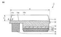
図1及び図2を参照して、実施の形態1に係る深紫外光を放射する半導体発光素子1は、主に、基板11と、n型半導体層12と、活性層13と、p型半導体層14と、n型電極15と、p型電極16とを備える。
(Embodiment 1)
1 and 2, semiconductor light-emitting element 1 that emits deep ultraviolet light according to the first embodiment mainly includes substrate 11, n-type semiconductor layer 12, active layer 13, and p-type semiconductor. A layer 14, an n-type electrode 15, and a p-type electrode 16 are provided.

基板11は、第1の主面11aと、第1の主面11aと反対側の第2の主面11bと、第1の主面11aと第2の主面11bとの間に延在する側面11cとを有する。第2の主面11bは、出射面であってもよい。半導体発光素子1の光取り出し効率を向上させるために、基板11は、半導体発光素子1が放射する深紫外光の波長に対して、例えば50%以上のような、高い透過率を有することが好ましい。基板11の材料として、窒化アルミニウム(AlN)、サファイア(Al23)を例示することができる。基板11は、物理的蒸気輸送(PVT)、ハイドライド気相成長(HVPE)のような方法によって製造されてもよい。ハイドライド気相成長(HVPE)によって製造された窒化アルミニウム(AlN)からなる基板11は、基板11の製造条件に依るが、例えば、330nm、265nm、220nmの波長において、それぞれ、5.6cm-1、9.0cm-1、14.5cm-1の光吸収係数αを有する。サファイア(Al23)からなる基板11は、基板11の製造方法及び製造条件に依るが、例えば、265nm、220mの波長において、それぞれ、1cm-1、9cm-1の光吸収係数αを有する。基板11は、半導体発光素子1から放射される深紫外光の波長において、1cm-1以上、好ましくは、0.1cm-1以上、さらに好ましくは0.01cm-1以上の光吸収係数αを有してもよい。 The substrate 11 extends between the first main surface 11a, the second main surface 11b opposite to the first main surface 11a, and the first main surface 11a and the second main surface 11b. And a side surface 11c. The second main surface 11b may be an exit surface. In order to improve the light extraction efficiency of the semiconductor light emitting device 1, the substrate 11 preferably has a high transmittance such as 50% or more with respect to the wavelength of deep ultraviolet light emitted from the semiconductor light emitting device 1. . Examples of the material of the substrate 11 include aluminum nitride (AlN) and sapphire (Al 2 O 3 ). The substrate 11 may be manufactured by a method such as physical vapor transport (PVT) or hydride vapor phase epitaxy (HVPE). The substrate 11 made of aluminum nitride (AlN) manufactured by hydride vapor phase epitaxy (HVPE) depends on the manufacturing conditions of the substrate 11. For example, at a wavelength of 330 nm, 265 nm, and 220 nm, 5.6 cm −1 , It has a light absorption coefficient α of 9.0 cm −1 and 14.5 cm −1 . The substrate 11 made of sapphire (Al 2 O 3 ) has a light absorption coefficient α of 1 cm −1 and 9 cm −1 at wavelengths of 265 nm and 220 m, for example, depending on the manufacturing method and manufacturing conditions of the substrate 11. . The substrate 11 has a light absorption coefficient α of 1 cm −1 or more, preferably 0.1 cm −1 or more, more preferably 0.01 cm −1 or more at the wavelength of deep ultraviolet light emitted from the semiconductor light emitting device 1. May be.

基板11の厚さの範囲は、後述するように、深紫外光に対する基板11の光吸収係数によって主に定まる。基板11は、好ましくは50μm以上、より好ましくは100μm以上の厚さを有してもよい。基板11の厚さは、基板11の第1の主面11aと第2の主面11bとの最短距離で定義される。基板11は50μm以上の厚さを有するため、半導体発光素子1の機械的強度が向上して、半導体発光素子1の取り扱いが容易になる。基板11は50μm以上の厚さを有するため、基板11が割れにくくなる。基板11は50μm以上の厚さを有するため、基板11と、活性層13を含む半導体層、n型電極15及びp型電極16との間の熱膨張係数の差に起因して発生する応力等により、基板11が反ることを抑制することができる。基板11の機械的な強度の向上及び基板11の反りの抑制は、半導体発光素子1の作製プロセスにおいて歩留りが低下すること、並びに、半導体発光素子1の信頼性及び品質が低下することを防ぐことができる。基板11を50μm以上に厚くできることは、基板11の厚みを薄くするプロセスを省略したり、基板11の厚みを薄くするプロセスに要する時間を短くすることができる。そのため、半導体発光素子1の製造コストを抑制し、半導体発光素子1の生産スループットを向上させることができる。   As will be described later, the thickness range of the substrate 11 is mainly determined by the light absorption coefficient of the substrate 11 with respect to deep ultraviolet light. The substrate 11 may have a thickness of preferably 50 μm or more, more preferably 100 μm or more. The thickness of the substrate 11 is defined by the shortest distance between the first main surface 11a and the second main surface 11b of the substrate 11. Since the substrate 11 has a thickness of 50 μm or more, the mechanical strength of the semiconductor light emitting device 1 is improved and the semiconductor light emitting device 1 can be easily handled. Since the substrate 11 has a thickness of 50 μm or more, the substrate 11 is difficult to break. Since the substrate 11 has a thickness of 50 μm or more, the stress generated due to the difference in thermal expansion coefficient between the substrate 11, the semiconductor layer including the active layer 13, the n-type electrode 15, and the p-type electrode 16. As a result, the substrate 11 can be prevented from warping. The improvement of the mechanical strength of the substrate 11 and the suppression of the warpage of the substrate 11 prevent the yield in the manufacturing process of the semiconductor light emitting element 1 from decreasing and the reliability and quality of the semiconductor light emitting element 1 from decreasing. Can do. If the substrate 11 can be thickened to 50 μm or more, the process of reducing the thickness of the substrate 11 can be omitted, or the time required for the process of reducing the thickness of the substrate 11 can be shortened. Therefore, the manufacturing cost of the semiconductor light emitting element 1 can be suppressed and the production throughput of the semiconductor light emitting element 1 can be improved.

基板11の側面11cは、基板11の第1の主面11aに対して傾斜している。本実施の形態では、基板11の側面11cの全てが、基板11の第1の主面11aに対して同じ角度で傾斜している。特定的には、基板11の第1の主面11aと側面11cとがなす角βの補角θは、20°以上70°以下、または、100°以上140°以下である。図1は、90°より小さい補角θを有する半導体発光素子1を示す。θ<90°である場合には、補角θは、20°以上70°以下、好ましくは20°以上60°以下、さらに好ましくは30°以上60°以下であってもよい。図2は、90°より大きい補角θを有する半導体発光素子1を示す。θ>90°である場合には、補角θは、100°以上140°以下、好ましくは110°以上140°以下であってもよい。θ>90°である場合には、基板11の厚さtは、t≦0.5wtan(180−θ)であることが好ましい。ここで、wは、基板11の第1の主面11aにおける幅である。t>0.5wtan(180−θ)であると、基板11の形状が逆三角形となり、実質的に基板11の厚さtが小さくなるからである。   The side surface 11 c of the substrate 11 is inclined with respect to the first main surface 11 a of the substrate 11. In the present embodiment, all of the side surfaces 11 c of the substrate 11 are inclined at the same angle with respect to the first main surface 11 a of the substrate 11. Specifically, the complementary angle θ of the angle β formed by the first main surface 11a and the side surface 11c of the substrate 11 is 20 ° or more and 70 ° or less, or 100 ° or more and 140 ° or less. FIG. 1 shows a semiconductor light emitting device 1 having a complementary angle θ smaller than 90 °. When θ <90 °, the complementary angle θ may be 20 ° to 70 °, preferably 20 ° to 60 °, and more preferably 30 ° to 60 °. FIG. 2 shows a semiconductor light emitting device 1 having a complementary angle θ greater than 90 °. When θ> 90 °, the complementary angle θ may be 100 ° to 140 °, preferably 110 ° to 140 °. When θ> 90 °, the thickness t of the substrate 11 is preferably t ≦ 0.5 wtan (180−θ). Here, w is the width of the first main surface 11 a of the substrate 11. This is because if t> 0.5 wtan (180−θ), the shape of the substrate 11 is an inverted triangle, and the thickness t of the substrate 11 is substantially reduced.

基板11の第1の主面11aの上に、n型半導体層12が設けられる。n型半導体層12は、AlInGaNからなる窒化物半導体から構成されてもよい。より特定的には、n型半導体層12は、Alx1Iny1Gaz1N(x1、y1、z1は、0≦x1≦1.0、0≦y1≦0.1、0≦z1≦1.0を満たす有理数とし、x1+y1+z1=1.0である)から構成されてもよい。n型半導体層12は、珪素(Si)、ゲルマニウム(Ge)、スズ(Sn)、酸素(O)、炭素(C)のようなn型不純物を含むことが好ましい。n型半導体層12におけるn型不純物の濃度は、1.0×1017cm-3以上1.0×1020cm-3以下、好ましくは、1.0×1018cm-3以上1.0×1019cm-3以下であってもよい。n型半導体層12は、100〜10000nm、好ましくは500〜3000nmの膜厚を有してもよい。基板11の側面11cと同様に、n型半導体層12の側面は、基板11の第1の主面11aに対して傾斜してもよい。 An n-type semiconductor layer 12 is provided on the first major surface 11 a of the substrate 11. The n-type semiconductor layer 12 may be made of a nitride semiconductor made of AlInGaN. More specifically, n-type semiconductor layer 12, Al x1 In y1 Ga z1 N (x 1, y 1, z 1 is, 0 ≦ x 1 ≦ 1.0,0 ≦ y 1 ≦ 0.1,0 ≦ z 1 ≦ 1.0, which is a rational number, and x 1 + y 1 + z 1 = 1.0). The n-type semiconductor layer 12 preferably contains an n-type impurity such as silicon (Si), germanium (Ge), tin (Sn), oxygen (O), or carbon (C). The concentration of the n-type impurity in the n-type semiconductor layer 12 is 1.0 × 10 17 cm −3 or more and 1.0 × 10 20 cm −3 or less, preferably 1.0 × 10 18 cm −3 or more and 1.0. It may be × 10 19 cm −3 or less. The n-type semiconductor layer 12 may have a thickness of 100 to 10000 nm, preferably 500 to 3000 nm. Similarly to the side surface 11 c of the substrate 11, the side surface of the n-type semiconductor layer 12 may be inclined with respect to the first main surface 11 a of the substrate 11.

n型半導体層12によって活性層13に電子及び正孔を閉じ込めるとともに、活性層13から放射される深紫外光がn型半導体層12によって吸収されることを抑制するために、n型半導体層12は、活性層13から放射される深紫外光のエネルギーよりも大きなバンドギャップエネルギーを有することが好ましい。n型半導体層12は、活性層13よりも低い屈折率を有し、クラッド層として機能してもよい。n型半導体層12は、単層から構成されてもよいし、Al組成、In組成、もしくはGa組成が互いに異なる複数層から構成されてもよい。Al組成、In組成、もしくはGa組成が互いに異なる複数層は、超格子構造、または、その組成が徐々に変化する傾斜組成構造を有してもよい。   In order to confine electrons and holes in the active layer 13 by the n-type semiconductor layer 12 and to suppress the deep ultraviolet light emitted from the active layer 13 from being absorbed by the n-type semiconductor layer 12, the n-type semiconductor layer 12. Preferably has a band gap energy larger than the energy of deep ultraviolet light emitted from the active layer 13. The n-type semiconductor layer 12 has a refractive index lower than that of the active layer 13 and may function as a cladding layer. The n-type semiconductor layer 12 may be composed of a single layer, or may be composed of a plurality of layers having different Al compositions, In compositions, or Ga compositions. A plurality of layers having different Al compositions, In compositions, or Ga compositions may have a superlattice structure or a graded composition structure in which the composition gradually changes.

n型半導体層12の上に、活性層13が設けられる。半導体発光素子1は、190nm以上350nm以下の波長を有する深紫外光を放射する。半導体発光素子1は、好ましくは200nm以上320nm以下、より好ましくは220nm以上300nm以下の波長を有する深紫外光を放射してもよい。特定的には、半導体発光素子1の活性層13から、190nm以上350nm以下の波長を有する深紫外光が放射される。本明細書において、半導体発光素子1から放射される深紫外光の波長は、半導体発光素子1から放射される深紫外光のピーク発光波長を意味してもよい。   An active layer 13 is provided on the n-type semiconductor layer 12. The semiconductor light emitting device 1 emits deep ultraviolet light having a wavelength of 190 nm or more and 350 nm or less. The semiconductor light emitting device 1 may emit deep ultraviolet light having a wavelength of preferably 200 nm to 320 nm, more preferably 220 nm to 300 nm. Specifically, deep ultraviolet light having a wavelength of 190 nm or more and 350 nm or less is emitted from the active layer 13 of the semiconductor light emitting device 1. In the present specification, the wavelength of deep ultraviolet light emitted from the semiconductor light emitting device 1 may mean the peak emission wavelength of deep ultraviolet light emitted from the semiconductor light emitting device 1.

活性層13は、AlInGaNからなる窒化物半導体から構成されてもよい。より特定的には、活性層13は、Alx2Iny2Gaz2N(x2、y2、z2は、0≦x2≦1.0、0≦y2≦0.1、0≦z2≦1.0を満たす有理数とし、x2+y2+z2=1.0である)から構成される井戸層と、井戸層よりもバンドギャップエネルギーが大きいAlx3Iny3Gaz3N(x3、y3、z3は、0≦x3≦1.0、0≦y3≦0.1、0≦z3≦1.0を満たす有理数とし、x3+y3+z3=1.0である)から構成される障壁層とを含む多重量子井戸(MQW)構造を有してもよい。n型半導体層12及びp型半導体層14によって活性層13に電子及び正孔を閉じ込めるために、活性層13は、n型半導体層12及びp型半導体層14よりも小さなバンドギャップエネルギーを有することが好ましい。活性層13は、n型半導体層12及びp型半導体層14よりも高い屈折率を有してもよい。 The active layer 13 may be made of a nitride semiconductor made of AlInGaN. More specifically, the active layer 13 is made of Al x2 In y2 Ga z2 N (x 2 , y 2 , z 2 are 0 ≦ x 2 ≦ 1.0, 0 ≦ y 2 ≦ 0.1, 0 ≦ z A well layer composed of rational numbers satisfying 2 ≦ 1.0 and x 2 + y 2 + z 2 = 1.0), and Al x3 In y3 Ga z3 N (x 3) having a larger band gap energy than the well layer , Y 3 and z 3 are rational numbers satisfying 0 ≦ x 3 ≦ 1.0, 0 ≦ y 3 ≦ 0.1, and 0 ≦ z 3 ≦ 1.0, and x 3 + y 3 + z 3 = 1.0 And a multi-quantum well (MQW) structure including a barrier layer composed of In order to confine electrons and holes in the active layer 13 by the n-type semiconductor layer 12 and the p-type semiconductor layer 14, the active layer 13 has a smaller band gap energy than the n-type semiconductor layer 12 and the p-type semiconductor layer 14. Is preferred. The active layer 13 may have a higher refractive index than the n-type semiconductor layer 12 and the p-type semiconductor layer 14.

活性層13の上に、p型半導体層14が設けられる。p型半導体層は、活性層13側に位置する第1のp型半導体層14aと、活性層13と反対側に位置する第2のp型半導体層14bとから構成されてもよい。   A p-type semiconductor layer 14 is provided on the active layer 13. The p-type semiconductor layer may be composed of a first p-type semiconductor layer 14 a located on the active layer 13 side and a second p-type semiconductor layer 14 b located on the opposite side to the active layer 13.

第1のp型半導体層14aは、AlInGaNからなる窒化物半導体から構成されてもよい。より特定的には、第1のp型半導体層14aは、Alx4Iny4Gaz4N(x4、y4、z4は、0≦x4≦1.0、0≦y4≦0.1、0≦z4≦1.0を満たす有理数とし、x4+y4+z4=1.0である)から構成されてもよい。第1のp型半導体層14aは、マグネシウム(Mg)、亜鉛(Zn)、ベリリウム(Be)のようなp型不純物を含むことが好ましい。第1のp型半導体層14aにおけるp型不純物の濃度は、1.0×1017cm-3以上、好ましくは、1.0×1018cm-3以上であってもよい。第1のp型半導体層14aは、5〜1000nm、好ましくは10〜500nm以下の膜厚を有してもよい。 The first p-type semiconductor layer 14a may be made of a nitride semiconductor made of AlInGaN. More specifically, the first p-type semiconductor layer 14a is made of Al x4 In y4 Ga z4 N (x 4 , y 4 , z 4 are 0 ≦ x 4 ≦ 1.0, 0 ≦ y 4 ≦ 0. 1 and a rational number satisfying 0 ≦ z 4 ≦ 1.0, and x 4 + y 4 + z 4 = 1.0). The first p-type semiconductor layer 14a preferably contains a p-type impurity such as magnesium (Mg), zinc (Zn), or beryllium (Be). The concentration of the p-type impurity in the first p-type semiconductor layer 14a may be 1.0 × 10 17 cm −3 or more, preferably 1.0 × 10 18 cm −3 or more. The first p-type semiconductor layer 14a may have a thickness of 5 to 1000 nm, preferably 10 to 500 nm or less.

第1のp型半導体層14aによって活性層13に電子及び正孔を閉じ込めるとともに、活性層13から放射される深紫外光が第1のp型半導体層14aによって吸収されることを抑制するために、第1のp型半導体層14aは、活性層13から放射される深紫外光のエネルギーよりも大きなバンドギャップエネルギーを有してもよい。第1のp型半導体層14aは、活性層13よりも低い屈折率を有し、クラッド層として機能してもよい。第1のp型半導体層14aは、単層から構成されてもよいし、Al組成、In組成、もしくはGa組成が互いに異なる複数層から構成されてもよい。Al組成、In組成、もしくはGa組成が互いに異なる複数層は、超格子構造、または、その組成が徐々に変化する傾斜組成構造を有してもよい。   In order to confine electrons and holes in the active layer 13 by the first p-type semiconductor layer 14a and to prevent deep ultraviolet light emitted from the active layer 13 from being absorbed by the first p-type semiconductor layer 14a. The first p-type semiconductor layer 14 a may have a band gap energy larger than the energy of deep ultraviolet light emitted from the active layer 13. The first p-type semiconductor layer 14a may have a refractive index lower than that of the active layer 13, and may function as a cladding layer. The first p-type semiconductor layer 14a may be composed of a single layer, or may be composed of a plurality of layers having different Al compositions, In compositions, or Ga compositions. A plurality of layers having different Al compositions, In compositions, or Ga compositions may have a superlattice structure or a graded composition structure in which the composition gradually changes.

第2のp型半導体層14bは、AlInGaNからなる窒化物半導体から構成されてもよい。より特定的には、第2のp型半導体層14bは、Alx5Iny5Gaz5N(x5、y5、z5は、0≦x5≦1.0、0≦y5≦0.1、0≦z5≦1.0を満たす有理数とし、x5+y5+z5=1.0である)から構成されてもよい。第2のp型半導体層14bは、マグネシウム(Mg)、亜鉛(Zn)、ベリリウム(Be)のようなp型不純物を含むことが好ましい。第2のp型半導体層14bは、第1のp型半導体層14aよりも高いp型伝導度を有し、p型コンタクト層として機能してもよい。第2のp型半導体層14bにおけるp型不純物の濃度は、1.0×1017cm-3以上、好ましくは、1.0×1018cm-3以上であってもよい。活性層13から放射される深紫外光が第2のp型半導体層14bによって吸収されることを抑制するためと、第2のp型半導体層14bにおいて良好なp型コンタクトを得るために、第2のp型半導体層14bは、1〜500nmの膜厚を有してもよい。 The second p-type semiconductor layer 14b may be made of a nitride semiconductor made of AlInGaN. More specifically, the second p-type semiconductor layer 14b is made of Al x5 In y5 Ga z5 N (x 5 , y 5 , z 5 are 0 ≦ x 5 ≦ 1.0, 0 ≦ y 5 ≦ 0. 1 and a rational number satisfying 0 ≦ z 5 ≦ 1.0, and x 5 + y 5 + z 5 = 1.0). The second p-type semiconductor layer 14b preferably contains a p-type impurity such as magnesium (Mg), zinc (Zn), or beryllium (Be). The second p-type semiconductor layer 14b has a higher p-type conductivity than the first p-type semiconductor layer 14a, and may function as a p-type contact layer. The concentration of the p-type impurity in the second p-type semiconductor layer 14b may be 1.0 × 10 17 cm −3 or more, preferably 1.0 × 10 18 cm −3 or more. In order to suppress the deep ultraviolet light emitted from the active layer 13 from being absorbed by the second p-type semiconductor layer 14b and to obtain a good p-type contact in the second p-type semiconductor layer 14b, The second p-type semiconductor layer 14b may have a thickness of 1 to 500 nm.

第1のp型半導体層14aと第2のp型半導体層14bとが窒化物半導体から構成される場合には、窒化物半導体のAl組成が小さくバンドギャップが小さいほど、第2のp型半導体層14bから活性層13により均一に正孔を注入することができ、良好なp型コンタクト特性を得ることができる。そのため、第2のp型半導体層14bは、小さなAl組成比を有してもよい。活性層13から放射される深紫外光が第2のp型半導体層14bによって吸収されることを抑制するために、第2のp型半導体層14bは、活性層13から放射される深紫外光のエネルギーよりも大きなバンドギャップエネルギーを有してもよい。   In the case where the first p-type semiconductor layer 14a and the second p-type semiconductor layer 14b are made of a nitride semiconductor, the second p-type semiconductor becomes smaller as the Al composition of the nitride semiconductor is smaller and the band gap is smaller. Holes can be uniformly injected from the layer 14b by the active layer 13, and good p-type contact characteristics can be obtained. Therefore, the second p-type semiconductor layer 14b may have a small Al composition ratio. In order to suppress the deep ultraviolet light emitted from the active layer 13 from being absorbed by the second p-type semiconductor layer 14b, the second p-type semiconductor layer 14b has a deep ultraviolet light emitted from the active layer 13. It may have a larger band gap energy than the energy of.

n型電極15は、n型半導体層12の露出面に設けられる。n型半導体層12の露出面は、基板11の上に、n型半導体層12、活性層13、及びp型半導体層14を積層した後、n型半導体層12の一部と、活性層13と、p型半導体層14とを部分的に除去することによって、n型半導体層12が露出した面を意味する。p型電極16は、p型半導体層14の表面、より特定的には、p型コンタクト層として機能してもよい第2のp型半導体層14bの表面に設けられる。   The n-type electrode 15 is provided on the exposed surface of the n-type semiconductor layer 12. The exposed surface of the n-type semiconductor layer 12 is formed by laminating the n-type semiconductor layer 12, the active layer 13, and the p-type semiconductor layer 14 on the substrate 11, and then a part of the n-type semiconductor layer 12 and the active layer 13. And the surface where the n-type semiconductor layer 12 is exposed by partially removing the p-type semiconductor layer 14. The p-type electrode 16 is provided on the surface of the p-type semiconductor layer 14, more specifically, on the surface of the second p-type semiconductor layer 14b that may function as a p-type contact layer.

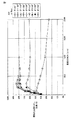
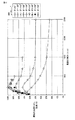
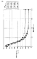
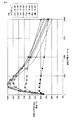
図3から図16に、基板11が窒化アルミニウム(AlN)で形成されるとともに、所定の光吸収係数α、所定の屈折率n及び800μmの幅wを有する場合の、基板11の厚さt及び補角θに対する半導体発光素子1の規格化光取り出し効率のシミュレーション結果を示す。図3から図16のそれぞれにおける半導体発光素子1の規格化光取り出し効率は、所定の光吸収係数α、所定の屈折率n、厚さtと、補角θとを有する基板11を備える半導体発光素子1の光取り出し効率を、当該所定の光吸収係数αと当該所定の屈折率nを有する基板11を備える半導体発光素子の光取り出し効率の最大値で割った値として定義される。例えば、図3及び図4を参照して、基板の屈折率nが2.29であり、基板11の光吸収係数α=1cm-1である場合には、補角θが20°である半導体発光素子1の光取り出し効率が最大となる。そこで、基板の屈折率nが2.29であり、基板11の光吸収係数α=1cm-1であり、補角θを有する半導体発光素子1の光取り出し効率を、基板の屈折率nが2.29であり、基板11の光吸収係数α=1cm-1であり、補角θが20°である半導体発光素子1の最大光取り出し効率で割った値が、図3及び図4に示されている。 3 to 16, when the substrate 11 is made of aluminum nitride (AlN) and has a predetermined light absorption coefficient α, a predetermined refractive index n, and a width w of 800 μm, the thickness t of the substrate 11 and The simulation result of the normalized light extraction efficiency of the semiconductor light emitting device 1 with respect to the complementary angle θ is shown. The normalized light extraction efficiency of the semiconductor light emitting device 1 in each of FIGS. 3 to 16 is that the semiconductor light emitting device includes a substrate 11 having a predetermined light absorption coefficient α, a predetermined refractive index n, a thickness t, and a complementary angle θ. It is defined as a value obtained by dividing the light extraction efficiency of the element 1 by the maximum value of the light extraction efficiency of the semiconductor light emitting element including the substrate 11 having the predetermined light absorption coefficient α and the predetermined refractive index n. For example, referring to FIGS. 3 and 4, when the refractive index n of the substrate is 2.29 and the light absorption coefficient α of the substrate 11 is 1 cm −1 , the semiconductor whose complementary angle θ is 20 °. The light extraction efficiency of the light emitting element 1 is maximized. Therefore, the refractive index n of the substrate is 2.29, the light absorption coefficient α of the substrate 11 is 1 cm −1 , and the light extraction efficiency of the semiconductor light-emitting element 1 having the complementary angle θ is as follows. .29, the light absorption coefficient α of the substrate 11 = 1 cm −1 , and the value divided by the maximum light extraction efficiency of the semiconductor light emitting device 1 having a complementary angle θ of 20 ° is shown in FIG. 3 and FIG. ing.

図3、5、7、9、11、13は、それぞれ、図1に示されるように補角θが90°より小さく、窒化アルミニウムで形成された基板の屈折率nが2.29であり、基板11の光吸収係数α=1cm-1、3cm-1、9cm-1、20cm-1、30cm-1、40cm-1である場合の、半導体発光素子1の規格化光取り出し効率のシミュレーション結果を示す。基板11の屈折率nは、基板11に入射する光の波長によってほぼ決まる。窒化アルミニウム(AlN)は、265nmの波長を有する深紫外光に対して、2.29の屈折率を有する。これに対し、基板11の光吸収係数αは、基板11に入射する光の波長及び基板11の製造方法等によって変化する。図3、5、7、9、11、13は、基板11の光吸収係数αを変化させたときの、265nmの波長を有する深紫外光を放射する半導体発光素子1の規格化光取り出し効率のシミュレーション結果を表す。 3, 5, 7, 9, 11, and 13, respectively, as shown in FIG. 1, the complementary angle θ is smaller than 90 °, and the refractive index n of the substrate formed of aluminum nitride is 2.29. light absorption coefficient alpha = 1 cm -1 of the substrate 11, 3cm -1, 9cm -1, 20cm -1, where 30 cm -1, is 40 cm -1, the simulation results of normalized light extraction efficiency of the semiconductor light emitting element 1 Show. The refractive index n of the substrate 11 is substantially determined by the wavelength of light incident on the substrate 11. Aluminum nitride (AlN) has a refractive index of 2.29 for deep ultraviolet light having a wavelength of 265 nm. On the other hand, the light absorption coefficient α of the substrate 11 varies depending on the wavelength of light incident on the substrate 11, the manufacturing method of the substrate 11, and the like. 3, 5, 7, 9, 11, and 13 show the normalized light extraction efficiency of the semiconductor light emitting device 1 that emits deep ultraviolet light having a wavelength of 265 nm when the light absorption coefficient α of the substrate 11 is changed. Represents simulation results.

図3、5、7、9、11、13を参照して、20°以上70°以下の補角θを有する基板11を備える本実施の形態の半導体発光素子1の規格化光取り出し効率は、90°の補角θを有する基板を備える比較例の半導体発光素子の規格化光取り出し効率より大きくなる。20°以上70°以下の補角θを有する基板11を備える本実施の形態の半導体発光素子1は、90°の補角θを有する基板を備える比較例の半導体発光素子の光取り出し効率よりも、向上した光取り出し効率を有する。第一に、基板11の第1の主面11aに対して基板11の側面11cを補角θで傾斜させることによって、基板11の側面11cの面積が大きくなるからである。第二に、基板11の第1の主面11aに対して基板11の側面11cを補角θで傾斜させることによって、基板11の側面11cで全反射される深紫外光の割合、及び基板11の側面11cで全反射された深紫外光が基板11の第2の主面11bでさらに全反射される深紫外光の割合を急速に減少するからである。   3, 5, 7, 9, 11, and 13, the normalized light extraction efficiency of the semiconductor light emitting device 1 of the present embodiment including the substrate 11 having the complementary angle θ of 20 ° or more and 70 ° or less is It becomes larger than the normalized light extraction efficiency of the semiconductor light emitting device of the comparative example including the substrate having the complementary angle θ of 90 °. The semiconductor light emitting device 1 of the present embodiment including the substrate 11 having the complementary angle θ of 20 ° or more and 70 ° or less is higher than the light extraction efficiency of the semiconductor light emitting device of the comparative example including the substrate having the complementary angle θ of 90 °. , With improved light extraction efficiency. First, the area of the side surface 11c of the substrate 11 is increased by inclining the side surface 11c of the substrate 11 with the complementary angle θ with respect to the first main surface 11a of the substrate 11. Second, the ratio of deep ultraviolet light totally reflected by the side surface 11c of the substrate 11 by tilting the side surface 11c of the substrate 11 with the complementary angle θ with respect to the first main surface 11a of the substrate 11, and the substrate 11 This is because the ratio of deep ultraviolet light that is totally reflected by the side surface 11 c of the substrate 11 is further totally reflected by the second main surface 11 b of the substrate 11.

図3、5、7、9、11、13を参照して、20°以上70°以下の補角θを有する本実施の形態の半導体発光素子1が小さな厚さtを有する基板11を備えるとき、基板11の厚さtが増加するにつれて、半導体発光素子1の規格化光取り出し効率が向上する。基板11の厚さtが増加するほど、傾斜した基板11の側面11cの面積が大きくなる。そのため、基板11の厚さtが増加するほど、活性層13から基板11の側面11cに入射する深紫外光の割合が増加する。基板11の厚さtが増加することによる、基板11の側面11cから出射される深紫外光の増加が、基板11の厚さtが増加することによる、基板11における深紫外光の吸収の増加よりも大きいため、基板11の厚さtが増加するにつれて、半導体発光素子1の規格化光取り出し効率が向上する。半導体発光素子1の規格化光取り出し効率は、ある基板11の厚さtmaxにおいて最大となり、基板11の厚さtがさらに大きくなると、半導体発光素子1の規格化光取り出し効率は減少する。基板11の厚さtがtmaxより大きい場合には、基板11の厚さtが増加することによる、基板11の側面11cから出射される深紫外光の増加よりも、基板11の厚さtが増加することによる、基板11における深紫外光の吸収の増加が大きくなるためである。以上に述べた、基板11の厚さtに対する半導体発光素子1の規格化光取り出し効率の変化は、基板11による光の吸収を無視することができない深紫外光を放射する半導体発光素子1に特有であり、基板による光の吸収が無視できるほど小さい可視または赤外の光を放射する半導体発光素子では見られない。 Referring to FIGS. 3, 5, 7, 9, 11, and 13, when semiconductor light emitting element 1 of the present embodiment having a complementary angle θ of 20 ° or more and 70 ° or less includes substrate 11 having a small thickness t. As the thickness t of the substrate 11 increases, the normalized light extraction efficiency of the semiconductor light emitting device 1 improves. As the thickness t of the substrate 11 increases, the area of the side surface 11c of the inclined substrate 11 increases. Therefore, as the thickness t of the substrate 11 increases, the ratio of deep ultraviolet light incident on the side surface 11c of the substrate 11 from the active layer 13 increases. The increase in deep ultraviolet light emitted from the side surface 11c of the substrate 11 due to the increase in the thickness t of the substrate 11 increases the absorption of deep ultraviolet light in the substrate 11 due to the increase in the thickness t of the substrate 11. Therefore, as the thickness t of the substrate 11 increases, the normalized light extraction efficiency of the semiconductor light emitting device 1 is improved. The normalized light extraction efficiency of the semiconductor light emitting element 1 is maximized at a thickness t max of a certain substrate 11, and the normalized light extraction efficiency of the semiconductor light emitting element 1 decreases as the thickness t of the substrate 11 further increases. When the thickness t of the substrate 11 is larger than t max , the thickness t of the substrate 11 is larger than the increase in deep ultraviolet light emitted from the side surface 11 c of the substrate 11 due to the increase in the thickness t of the substrate 11. This is because the increase in the absorption of deep ultraviolet light in the substrate 11 due to the increase in the resistance increases. The above-described change in the normalized light extraction efficiency of the semiconductor light emitting device 1 with respect to the thickness t of the substrate 11 is peculiar to the semiconductor light emitting device 1 that emits deep ultraviolet light whose light absorption by the substrate 11 cannot be ignored. This is not seen in semiconductor light emitting devices that emit visible or infrared light that is so small that light absorption by the substrate is negligible.

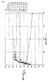
図4、6、8、10、12、14は、それぞれ、図2に示されるように補角θが90°より大きく、窒化アルミニウムで形成された基板の屈折率nが2.29であり、基板11の光吸収係数α=1cm-1、3cm-1、9cm-1、20cm-1、30cm-1、40cm-1である場合の、半導体発光素子1の規格化光取り出し効率を示す。図4、6、8、10、12、14は、基板11の光吸収係数αを変化させたときの、265nmの波長を有する深紫外光を放射する半導体発光素子1の規格化光取り出し効率のシミュレーション結果を表す。 4, 6, 8, 10, 12, and 14, respectively, as shown in FIG. 2, the complementary angle θ is larger than 90 °, and the refractive index n of the substrate formed of aluminum nitride is 2.29. The normalized light extraction efficiency of the semiconductor light emitting device 1 when the light absorption coefficient α of the substrate 11 is 1 cm −1 , 3 cm −1 , 9 cm −1 , 20 cm −1 , 30 cm −1 , and 40 cm −1 is shown. 4, 6, 8, 10, 12, and 14 show the normalized light extraction efficiency of the semiconductor light emitting device 1 that emits deep ultraviolet light having a wavelength of 265 nm when the light absorption coefficient α of the substrate 11 is changed. Represents the simulation result.

図4、6、8、10、12、14を参照して、100°以上140°以下の補角θを有する基板11を備える本実施の形態の半導体発光素子1の規格化光取り出し効率は、90°の補角θを有する基板を備える比較例の半導体発光素子の規格化光取り出し効率より大きくなる。100°以上140°以下の補角θを有する基板11を備える本実施の形態の半導体発光素子1は、90°の補角θを有する基板を備える比較例の半導体発光素子の光取り出し効率よりも、向上した光取り出し効率を有する。第一に、基板11の第1の主面11aに対して基板11の側面11cを補角θで傾斜させることによって、基板11の側面11cの面積が大きくなり、活性層13から基板11の側面11cに入射する深紫外光の割合が増加するからである。第二に、基板11の第1の主面11aに対して基板11の側面11cを補角θで傾斜させることによって、基板11の側面11cで全反射される深紫外光の割合、及び基板11の側面11cで全反射された深紫外光が基板11の第2の主面11bでさらに全反射される深紫外光の割合を急速に減少するからである。   Referring to FIGS. 4, 6, 8, 10, 12, and 14, the normalized light extraction efficiency of the semiconductor light emitting device 1 of the present embodiment including the substrate 11 having the complementary angle θ of 100 ° or more and 140 ° or less is It becomes larger than the normalized light extraction efficiency of the semiconductor light emitting device of the comparative example including the substrate having the complementary angle θ of 90 °. The semiconductor light emitting device 1 of the present embodiment including the substrate 11 having the complementary angle θ of 100 ° or more and 140 ° or less is more than the light extraction efficiency of the semiconductor light emitting device of the comparative example including the substrate having the complementary angle θ of 90 °. , With improved light extraction efficiency. First, by inclining the side surface 11c of the substrate 11 with the complementary angle θ with respect to the first main surface 11a of the substrate 11, the area of the side surface 11c of the substrate 11 is increased, and the side surface of the substrate 11 from the active layer 13 is increased. This is because the proportion of deep ultraviolet light incident on 11c increases. Second, the ratio of deep ultraviolet light totally reflected by the side surface 11c of the substrate 11 by tilting the side surface 11c of the substrate 11 with the complementary angle θ with respect to the first main surface 11a of the substrate 11, and the substrate 11 This is because the ratio of deep ultraviolet light that is totally reflected by the side surface 11 c of the substrate 11 is further totally reflected by the second main surface 11 b of the substrate 11.

図4、6、8、10、12、14を参照して、100°以上140°以下の補角θを有する本実施の形態の半導体発光素子1が小さな厚さtを有する基板11を備えるとき、基板11の厚さtが増加するにつれて、半導体発光素子1の規格化光取り出し効率が向上する。基板11の厚さtが増加するほど、傾斜した基板11の側面11cの面積が大きくなる。そのため、基板11の厚さtが増加するほど、活性層13から基板11の側面11cに入射する深紫外光の割合が増加する。基板11の厚さtが増加することによる、基板11の側面11cから出射される深紫外光の増加が、基板11の厚さtが増加することによる、基板11における深紫外光の吸収の増加よりも大きいため、基板11の厚さtが増加するにつれて、半導体発光素子1の規格化光取り出し効率が向上する。半導体発光素子1の規格化光取り出し効率は、ある基板11の厚さtmaxにおいて最大となり、基板11の厚さtがさらに大きくなると、半導体発光素子1の規格化光取り出し効率は減少する。基板11の厚さtがtmaxより大きい場合には、基板11の厚さtが増加することによる、基板11の側面11cから出射される深紫外光の増加よりも、基板11の厚さtが増加することによる、基板11における深紫外光の吸収の増加が大きくなるためである。以上に述べた、基板11の厚さtに対する半導体発光素子1の規格化光取り出し効率の変化は、基板11による光の吸収を無視することができない深紫外光を放射する半導体発光素子1に特有であり、基板による光の吸収が無視できるほど小さい可視または赤外の光を放射する半導体発光素子では見られない。 4, 6, 8, 10, 12, and 14, when the semiconductor light emitting device 1 of the present embodiment having a complementary angle θ of 100 ° or more and 140 ° or less includes a substrate 11 having a small thickness t. As the thickness t of the substrate 11 increases, the normalized light extraction efficiency of the semiconductor light emitting device 1 improves. As the thickness t of the substrate 11 increases, the area of the side surface 11c of the inclined substrate 11 increases. Therefore, as the thickness t of the substrate 11 increases, the ratio of deep ultraviolet light incident on the side surface 11c of the substrate 11 from the active layer 13 increases. The increase in deep ultraviolet light emitted from the side surface 11c of the substrate 11 due to the increase in the thickness t of the substrate 11 increases the absorption of deep ultraviolet light in the substrate 11 due to the increase in the thickness t of the substrate 11. Therefore, as the thickness t of the substrate 11 increases, the normalized light extraction efficiency of the semiconductor light emitting device 1 is improved. The normalized light extraction efficiency of the semiconductor light emitting element 1 is maximized at a thickness t max of a certain substrate 11, and the normalized light extraction efficiency of the semiconductor light emitting element 1 decreases as the thickness t of the substrate 11 further increases. When the thickness t of the substrate 11 is larger than t max , the thickness t of the substrate 11 is larger than the increase in deep ultraviolet light emitted from the side surface 11 c of the substrate 11 due to the increase in the thickness t of the substrate 11. This is because the increase in the absorption of deep ultraviolet light in the substrate 11 due to the increase in the resistance increases. The above-described change in the normalized light extraction efficiency of the semiconductor light emitting device 1 with respect to the thickness t of the substrate 11 is peculiar to the semiconductor light emitting device 1 that emits deep ultraviolet light whose light absorption by the substrate 11 cannot be ignored. This is not seen in semiconductor light emitting devices that emit visible or infrared light that is so small that light absorption by the substrate is negligible.

また、90°より大きい補角θを有する半導体発光素子1は、90°より小さい補角θを有する半導体発光素子1よりも、基板11の厚さtが増加しても、規格化光取り出し効率が減少しにくい。これは、90°より大きい補角θを有する半導体発光素子1における、基板11の側面11cから出射される深紫外光の基板11内の経路長が、90°より小さい補角θを有する半導体発光素子1における、基板11の側面11cから出射される深紫外光の基板11内の経路長よりも短く(図18(A)及び(B)を参照)、90°より大きい補角θを有する半導体発光素子1は、90°より小さい補角θを有する半導体発光素子1よりも、基板11に吸収される深紫外光が少なくなるからである。   Further, the semiconductor light emitting device 1 having a complementary angle θ larger than 90 ° has a normalized light extraction efficiency even when the thickness t of the substrate 11 is increased as compared with the semiconductor light emitting device 1 having a complementary angle θ smaller than 90 °. Is difficult to decrease. This is because the semiconductor light emitting device 1 having a complementary angle θ larger than 90 ° has a path length in the substrate 11 of deep ultraviolet light emitted from the side surface 11c of the substrate 11 and has a complementary angle θ smaller than 90 °. In the element 1, a semiconductor having a complementary angle θ that is shorter than the path length in the substrate 11 of the deep ultraviolet light emitted from the side surface 11c of the substrate 11 (see FIGS. 18A and 18B) and larger than 90 °. This is because the light emitting element 1 absorbs less deep ultraviolet light than the semiconductor light emitting element 1 having a complementary angle θ smaller than 90 °.

図15は、図1に示されるように補角θが90°より小さく、基板の屈折率nが2.18であり、基板11の光吸収係数α=5.6cm-1である場合の、半導体発光素子1の規格化光取り出し効率のシミュレーション結果を示す。基板11の屈折率nは、基板11に入射する光の波長によってほぼ決まる。窒化アルミニウム(AlN)は、330nmの波長を有する深紫外光に対して、2.18の屈折率を有する。図15は、窒化アルミニウムで形成された基板11が5.6cm-1の光吸収係数αを有するときの、330nmの波長を有する深紫外光を放射する半導体発光素子1の規格化光取り出し効率のシミュレーション結果を表す。図15に示される半導体発光素子1の規格化光取り出し効率の変化は、図3、5、7、9、11、13に示される半導体発光素子1の規格化光取り出し効率の変化と同様の傾向を示す。基板11の屈折率nが変化しても、すなわち、半導体発光素子1の発光波長が変化しても、半導体発光素子1の規格化光取り出し効率を効果的に向上させることができる補角θ、厚さt及び光吸収係数αの範囲は大きく変化しないことが分かる。 FIG. 15 shows a case where the complementary angle θ is smaller than 90 ° as shown in FIG. 1, the refractive index n of the substrate is 2.18, and the light absorption coefficient α of the substrate 11 is 5.6 cm −1 . The simulation result of the normalized light extraction efficiency of the semiconductor light emitting device 1 is shown. The refractive index n of the substrate 11 is substantially determined by the wavelength of light incident on the substrate 11. Aluminum nitride (AlN) has a refractive index of 2.18 for deep ultraviolet light having a wavelength of 330 nm. FIG. 15 shows the normalized light extraction efficiency of the semiconductor light emitting device 1 that emits deep ultraviolet light having a wavelength of 330 nm when the substrate 11 formed of aluminum nitride has a light absorption coefficient α of 5.6 cm −1 . Represents simulation results. The change in the normalized light extraction efficiency of the semiconductor light emitting device 1 shown in FIG. 15 has the same tendency as the change in the normalized light extraction efficiency of the semiconductor light emitting device 1 shown in FIGS. 3, 5, 7, 9, 11, and 13. Indicates. Even if the refractive index n of the substrate 11 changes, that is, even if the emission wavelength of the semiconductor light emitting device 1 changes, the complementary angle θ that can effectively improve the normalized light extraction efficiency of the semiconductor light emitting device 1, It can be seen that the ranges of the thickness t and the light absorption coefficient α do not change greatly.

図16は、図2に示されるように補角θが90°より大きく、基板の屈折率nが2.18であり、基板11の光吸収係数α=5.6cm-1である場合の、半導体発光素子1の規格化光取り出し効率のシミュレーション結果を示す。基板11の屈折率nは、基板11に入射する光の波長によってほぼ決まる。窒化アルミニウム(AlN)は、330nmの波長を有する深紫外光に対して、2.18の屈折率を有する。図16は、窒化アルミニウムで形成された基板11が5.6cm-1の光吸収係数αを有するときの、330nmの波長を有する深紫外光を放射する半導体発光素子1の規格化光取り出し効率のシミュレーション結果を表す。図16に示される半導体発光素子1の規格化光取り出し効率の変化は、図4、6、8、10、12、14に示される半導体発光素子1の規格化光取り出し効率の変化と同様の傾向を示す。基板11の屈折率nが変化しても、すなわち、半導体発光素子1の発光波長が変化しても、半導体発光素子1の規格化光取り出し効率を効果的に向上させることができる補角θ、厚さt及び光吸収係数αの範囲は大きく変化しないことが分かる。 FIG. 16 shows a case where the complementary angle θ is larger than 90 ° as shown in FIG. 2, the refractive index n of the substrate is 2.18, and the light absorption coefficient α of the substrate 11 is 5.6 cm −1 . The simulation result of the normalized light extraction efficiency of the semiconductor light emitting device 1 is shown. The refractive index n of the substrate 11 is substantially determined by the wavelength of light incident on the substrate 11. Aluminum nitride (AlN) has a refractive index of 2.18 for deep ultraviolet light having a wavelength of 330 nm. FIG. 16 shows the normalized light extraction efficiency of the semiconductor light emitting device 1 that emits deep ultraviolet light having a wavelength of 330 nm when the substrate 11 formed of aluminum nitride has a light absorption coefficient α of 5.6 cm −1 . Represents the simulation result. The change in the normalized light extraction efficiency of the semiconductor light emitting device 1 shown in FIG. 16 has the same tendency as the change in the normalized light extraction efficiency of the semiconductor light emitting device 1 shown in FIGS. 4, 6, 8, 10, 12, and 14. Indicates. Even if the refractive index n of the substrate 11 changes, that is, even if the emission wavelength of the semiconductor light emitting device 1 changes, the complementary angle θ that can effectively improve the normalized light extraction efficiency of the semiconductor light emitting device 1, It can be seen that the ranges of the thickness t and the light absorption coefficient α do not change greatly.

図17は、図3から図16に示されるシミュレーション結果から得られた、半導体発光素子1の規格化光取り出し効率が50%となる、基板11の光吸収係数α(cm-1)及び基板11の厚さt(μm)の範囲を示す図である。図17に示される一方の点線は、20°以上70°以下または100°以上140°以下の補角θを有する基板11を備える半導体発光素子1の規格化光取り出し効率が50%となる基板の上限厚さの近似線t=3200α-0.7である。図17に示される他方の点線は、20°以上70°以下または100°以上140°以下の補角θを有する基板11を備える半導体発光素子1の規格化光取り出し効率が50%となる基板の下限厚さの近似線t=340exp(−0.16α)である。図17を参照して、基板11の光吸収係数α(cm-1)及び基板11の厚さt(μm)がこの2本の点線の間に位置する場合に、半導体発光素子1の規格化光取り出し効率が50%以上となる。具体的には、基板11の第1の主面11aと少なくとも一部の側面11cとがなす角の補角θが、20°以上70°以下、または、100°以上140°以下であり、かつ、基板11の光吸収係数α(cm-1)及び基板11の厚さt(μm)が、340exp(−0.16α)≦t≦3200α-0.7を満たす場合に、半導体発光素子1の規格化光取り出し効率が50%以上となる。このように、基板11の光吸収係数α(cm-1)、基板11の厚さt(μm)及び基板11の補角θを定めることによって、本実施の形態の半導体発光素子1の光取り出し効率は、90°の補角θを有する基板を備える比較例の半導体発光素子よりも、向上した光取り出し効率を有する。半導体発光素子1から放射される深紫外光の一部が基板11で吸収されることを考慮することによってはじめて、深紫外光を放射する半導体発光素子1の光取り出し効率を向上させることができる基板11を正確に設計することができる。 FIG. 17 shows the light absorption coefficient α (cm −1 ) of the
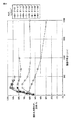
 substrate 11 and the substrate 11 which are obtained from the simulation results shown in FIGS. 3 to 16 and the normalized light extraction efficiency of the semiconductor light emitting device 1 is 50%. It is a figure which shows the range of thickness t (micrometer). One dotted line shown in FIG. 17 indicates that the normalized light extraction efficiency of the semiconductor light emitting device 1 including the substrate 11 having the complementary angle θ of 20 ° to 70 ° or 100 ° to 140 ° is 50%. Approximate line of upper limit thickness t = 3200α −0.7 . The other dotted line shown in FIG. 17 indicates that the normalized light extraction efficiency of the semiconductor light emitting device 1 including the substrate 11 having the complementary angle θ of 20 ° to 70 ° or 100 ° to 140 ° is 50%. The approximate line t of the lower limit thickness is t = 340 exp (−0.16α). Referring to FIG. 17, when the light absorption coefficient α (cm −1 ) of the substrate 11 and the thickness t (μm) of the substrate 11 are located between the two dotted lines, the standardization of the semiconductor light emitting element 1 is performed. The light extraction efficiency is 50% or more. Specifically, the complementary angle θ of the angle formed between the first main surface 11a of the substrate 11 and at least a part of the side surface 11c is 20 ° to 70 °, or 100 ° to 140 °, and When the light absorption coefficient α (cm −1 ) of the substrate 11 and the thickness t (μm) of the substrate 11 satisfy 340exp (−0.16α) ≦ t ≦ 3200α− 0.7 , standardization of the semiconductor light emitting device 1 The light extraction efficiency is 50% or more. As described above, by determining the light absorption coefficient α (cm −1 ) of the substrate 11, the thickness t (μm) of the substrate 11, and the complementary angle θ of the substrate 11, the light extraction of the semiconductor light emitting device 1 of the present embodiment. The efficiency is higher than that of the semiconductor light emitting device of the comparative example including the substrate having the complementary angle θ of 90 °. A substrate that can improve the light extraction efficiency of the semiconductor light emitting device 1 that emits deep ultraviolet light only by considering that a part of the deep ultraviolet light emitted from the semiconductor light emitting device 1 is absorbed by the substrate 11. 11 can be designed accurately.

図19から図22に、基板11がサファイア(Al23)で形成されるとともに、所定の光吸収係数α、所定の屈折率n及び800μmの幅wを有する場合の、基板11の厚さt及び補角θに対する半導体発光素子1の規格化光取り出し効率のシミュレーション結果を示す。図19から図22のそれぞれにおける半導体発光素子1の規格化光取り出し効率は、所定の光吸収係数α、所定の屈折率n、厚さtと、補角θとを有する基板11を備える半導体発光素子1の光取り出し効率を、当該所定の光吸収係数αと当該所定の屈折率nを有する基板11を備える半導体発光素子の光取り出し効率の最大値で割った値として定義される。例えば、図19及び図20を参照して、基板の屈折率nが1.88であり、基板11の光吸収係数α=9cm-1である場合には、補角θが35°である半導体発光素子1の光取り出し効率が最大となる。そこで、基板の屈折率nが1.88であり、基板11の光吸収係数α=9cm-1であり、補角θを有する半導体発光素子1の光取り出し効率を、基板の屈折率nが1.88であり、基板11の光吸収係数α=9cm-1であり、補角θが35°である半導体発光素子1の最大光取り出し効率で割った値が、図19及び図20に示されている。 19 to 22, the thickness of the substrate 11 when the substrate 11 is formed of sapphire (Al 2 O 3 ) and has a predetermined light absorption coefficient α, a predetermined refractive index n, and a width w of 800 μm. The simulation result of the normalized light extraction efficiency of the semiconductor light emitting device 1 with respect to t and the complementary angle θ is shown. The normalized light extraction efficiency of the semiconductor light emitting device 1 in each of FIGS. 19 to 22 is that semiconductor light emission including a substrate 11 having a predetermined light absorption coefficient α, a predetermined refractive index n, a thickness t, and a complementary angle θ. It is defined as a value obtained by dividing the light extraction efficiency of the element 1 by the maximum value of the light extraction efficiency of the semiconductor light emitting element including the substrate 11 having the predetermined light absorption coefficient α and the predetermined refractive index n. For example, referring to FIGS. 19 and 20, when the refractive index n of the substrate is 1.88 and the light absorption coefficient α of the substrate 11 is 9 cm −1 , the semiconductor whose complementary angle θ is 35 °. The light extraction efficiency of the light emitting element 1 is maximized. Accordingly, the refractive index n of the substrate is 1.88, the light absorption coefficient α of the substrate 11 is 9 cm −1 , and the light extraction efficiency of the semiconductor light-emitting element 1 having the complementary angle θ is as follows. .88, the light absorption coefficient α of the substrate 11 is 9 cm −1 , and the value divided by the maximum light extraction efficiency of the semiconductor light emitting device 1 having a complementary angle θ of 35 ° is shown in FIGS. ing.

図19は、図1に示されるように補角θが90°より小さく、基板の屈折率nが1.88であり、基板11の光吸収係数α=9cm-1である場合の、半導体発光素子1の規格化光取り出し効率のシミュレーション結果を示す。基板11の屈折率nは、基板11に入射する光の波長によってほぼ決まる。サファイア(Al23)は、220nmの波長を有する深紫外光に対して、1.88の屈折率を有する。図19は、サファイアで形成された基板11が9cm-1の光吸収係数αを有するときの、220nmの波長を有する深紫外光を放射する半導体発光素子1の規格化光取り出し効率のシミュレーション結果を表す。図21は、図1に示されるように補角θが90°より小さく、基板の屈折率nが1.80であり、基板11の光吸収係数α=1cm-1である場合の、半導体発光素子1の規格化光取り出し効率のシミュレーション結果を示す。基板11の屈折率nは、基板11に入射する光の波長によってほぼ決まる。サファイア(Al23)は、265nmの波長を有する深紫外光に対して、1.80の屈折率を有する。図21は、サファイアで形成された基板11が1cm-1の光吸収係数αを有するときの、265nmの波長を有する深紫外光を放射する半導体発光素子1の規格化光取り出し効率のシミュレーション結果を表す。 19 shows semiconductor light emission when the complementary angle θ is smaller than 90 °, the refractive index n of the substrate is 1.88, and the light absorption coefficient α of the substrate 11 is 9 cm −1 as shown in FIG. The simulation result of the normalized light extraction efficiency of the element 1 is shown. The refractive index n of the substrate 11 is substantially determined by the wavelength of light incident on the substrate 11. Sapphire (Al 2 O 3 ) has a refractive index of 1.88 for deep ultraviolet light having a wavelength of 220 nm. FIG. 19 shows the simulation result of the normalized light extraction efficiency of the semiconductor light emitting device 1 that emits deep ultraviolet light having a wavelength of 220 nm when the substrate 11 made of sapphire has a light absorption coefficient α of 9 cm −1. Represent. FIG. 21 shows semiconductor light emission when the complementary angle θ is smaller than 90 ° as shown in FIG. 1, the refractive index n of the substrate is 1.80, and the light absorption coefficient α = 1 cm −1 of the substrate 11. The simulation result of the normalized light extraction efficiency of the element 1 is shown. The refractive index n of the substrate 11 is substantially determined by the wavelength of light incident on the substrate 11. Sapphire (Al 2 O 3 ) has a refractive index of 1.80 for deep ultraviolet light having a wavelength of 265 nm. FIG. 21 shows a simulation result of the normalized light extraction efficiency of the semiconductor light emitting device 1 that emits deep ultraviolet light having a wavelength of 265 nm when the substrate 11 formed of sapphire has a light absorption coefficient α of 1 cm −1. Represent.

図19及び図21を参照して、20°以上70°以下の補角θを有する本実施の形態の半導体発光素子1は、図3、5、7、9、11、13に示される半導体発光素子1の規格化光取り出し効率の変化と同様の傾向を示す。具体的には、本実施の形態の半導体発光素子1の規格化光取り出し効率は、ある基板11の厚さtmaxにおいて最大となる。このような、基板11の厚さtに対する半導体発光素子1の規格化光取り出し効率の変化は、基板11による光の吸収を無視することができない深紫外光を放射する半導体発光素子1に特有であり、基板による光の吸収が無視できるほど小さい可視または赤外の光を放射する半導体発光素子では見られない。 Referring to FIGS. 19 and 21, the semiconductor light emitting device 1 of the present embodiment having a complementary angle θ of 20 ° or more and 70 ° or less is a semiconductor light emitting device shown in FIGS. The same tendency as the change in the normalized light extraction efficiency of the element 1 is shown. Specifically, the normalized light extraction efficiency of the semiconductor light emitting device 1 of the present embodiment is maximized at a thickness t max of a certain substrate 11. Such a change in the normalized light extraction efficiency of the semiconductor light emitting device 1 with respect to the thickness t of the substrate 11 is peculiar to the semiconductor light emitting device 1 that emits deep ultraviolet light whose light absorption by the substrate 11 cannot be ignored. In addition, it cannot be seen in a semiconductor light emitting device that emits visible or infrared light that is negligibly small in light absorption by the substrate.

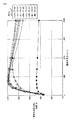
図20は、図2に示されるように補角θが90°より大きく、基板の屈折率nが1.88であり、基板11の光吸収係数α=9cm-1である場合の、半導体発光素子1の規格化光取り出し効率のシミュレーション結果を示す。サファイア(Al23)は、220nmの波長を有する深紫外光に対して、1.88の屈折率を有する。図20は、サファイアで形成された基板11が9cm-1の光吸収係数αを有するときの、220nmの波長を有する深紫外光を放射する半導体発光素子1の規格化光取り出し効率のシミュレーション結果を表す。図22は、図2に示されるように補角θが90°より大きく、基板の屈折率nが1.80であり、基板11の光吸収係数α=1cm-1である場合の、半導体発光素子1の規格化光取り出し効率のシミュレーション結果を示す。サファイア(Al23)は、265nmの波長を有する深紫外光に対して、1.80の屈折率を有する。図22は、サファイアで形成された基板11が1cm-1の光吸収係数αを有するときの、265nmの波長を有する深紫外光を放射する半導体発光素子1の規格化光取り出し効率のシミュレーション結果を表す。 FIG. 20 shows semiconductor light emission when the complementary angle θ is larger than 90 °, the refractive index n of the substrate is 1.88, and the light absorption coefficient α of the substrate 11 is 9 cm −1 as shown in FIG. The simulation result of the normalized light extraction efficiency of the element 1 is shown. Sapphire (Al 2 O 3 ) has a refractive index of 1.88 for deep ultraviolet light having a wavelength of 220 nm. FIG. 20 shows a simulation result of the normalized light extraction efficiency of the semiconductor light emitting device 1 that emits deep ultraviolet light having a wavelength of 220 nm when the substrate 11 made of sapphire has a light absorption coefficient α of 9 cm −1. Represent. FIG. 22 shows semiconductor light emission when the complementary angle θ is larger than 90 °, the refractive index n of the substrate is 1.80, and the light absorption coefficient α = 1 cm −1 of the substrate 11 as shown in FIG. The simulation result of the normalized light extraction efficiency of the element 1 is shown. Sapphire (Al 2 O 3 ) has a refractive index of 1.80 for deep ultraviolet light having a wavelength of 265 nm. FIG. 22 shows the simulation result of the normalized light extraction efficiency of the semiconductor light emitting device 1 that emits deep ultraviolet light having a wavelength of 265 nm when the substrate 11 formed of sapphire has a light absorption coefficient α of 1 cm −1. Represent.

図20及び図22を参照して、100°以上140°以下の補角θを有する本実施の形態の半導体発光素子1は、図4、6、8、10、12、14に示される半導体発光素子1の規格化光取り出し効率の変化と同様の傾向を示す。具体的には、本実施の形態の半導体発光素子1の規格化光取り出し効率は、ある基板11の厚さtmaxにおいて最大となる。このような、基板11の厚さtに対する半導体発光素子1の規格化光取り出し効率の変化は、基板11による光の吸収を無視することができない深紫外光を放射する半導体発光素子1に特有であり、基板による光の吸収が無視できるほど小さい可視または赤外の光を放射する半導体発光素子では見られない。また、90°より大きい補角θを有する半導体発光素子1は、90°より小さい補角θを有する半導体発光素子1よりも、基板11の厚さtが増加しても、規格化光取り出し効率が減少しにくい。これは、90°より大きい補角θを有する半導体発光素子1における、基板11の側面11cから出射される深紫外光の基板11内の経路長が、90°より小さい補角θを有する半導体発光素子1における、基板11の側面11cから出射される深紫外光の基板11内の経路長よりも短く(図18(A)及び(B)を参照)、90°より大きい補角θを有する半導体発光素子1は、90°より小さい補角θを有する半導体発光素子1よりも、基板11に吸収される深紫外光が少なくなるからである。 Referring to FIGS. 20 and 22, the semiconductor light emitting device 1 of the present embodiment having a complementary angle θ of 100 ° or more and 140 ° or less is a semiconductor light emitting device shown in FIGS. The same tendency as the change in the normalized light extraction efficiency of the element 1 is shown. Specifically, the normalized light extraction efficiency of the semiconductor light emitting device 1 of the present embodiment is maximized at a thickness t max of a certain substrate 11. Such a change in the normalized light extraction efficiency of the semiconductor light emitting device 1 with respect to the thickness t of the substrate 11 is peculiar to the semiconductor light emitting device 1 that emits deep ultraviolet light whose light absorption by the substrate 11 cannot be ignored. In addition, it cannot be seen in a semiconductor light emitting device that emits visible or infrared light that is negligibly small in light absorption by the substrate. Further, the semiconductor light emitting device 1 having a complementary angle θ larger than 90 ° has a normalized light extraction efficiency even when the thickness t of the substrate 11 is increased as compared with the semiconductor light emitting device 1 having a complementary angle θ smaller than 90 °. Is difficult to decrease. This is because the semiconductor light emitting device 1 having a complementary angle θ larger than 90 ° has a path length in the substrate 11 of deep ultraviolet light emitted from the side surface 11c of the substrate 11 and has a complementary angle θ smaller than 90 °. In the element 1, a semiconductor having a complementary angle θ that is shorter than the path length in the substrate 11 of the deep ultraviolet light emitted from the side surface 11c of the substrate 11 (see FIGS. 18A and 18B) and larger than 90 °. This is because the light emitting element 1 absorbs less deep ultraviolet light than the semiconductor light emitting element 1 having a complementary angle θ smaller than 90 °.

図23は、図19から図22に示されるシミュレーション結果から得られた、半導体発光素子1の規格化光取り出し効率が50%以上となる、基板11の光吸収係数α(cm-1)及び基板11の厚さt(μm)の範囲を示す図である。図23に示される一方の点線は、t=3200α-0.7を表す線である。図23に示される他方の点線は、t=340exp(−0.16α)を表す線である。図23を参照して、基板11の光吸収係数α(cm-1)及び基板11の厚さt(μm)がこれら2本の点線の間に位置すれば、半導体発光素子1の規格化光取り出し効率が50%以上となる。具体的には、基板11の第1の主面11aと少なくとも一部の側面11cとがなす角の補角θが、20°以上70°以下、または、100°以上140°以下であり、かつ、基板11の光吸収係数α(cm-1)及び基板11の厚さt(μm)が、340exp(−0.16α)≦t≦3200α-0.7を満たす場合に、半導体発光素子1の規格化光取り出し効率が50%以上となる。このように、基板11の光吸収係数α(cm-1)、基板11の厚さt(μm)及び基板11の補角θを定めることによって、本実施の形態の半導体発光素子1の光取り出し効率は、90°の補角θを有する基板を備える比較例の半導体発光素子よりも、向上した光取り出し効率を有する。半導体発光素子1から放射される深紫外光の一部が基板11で吸収されることを考慮することによってはじめて、深紫外光を放射する半導体発光素子1の光取り出し効率を向上させることができる基板11を正確に設計することができる。 FIG. 23 shows the light absorption coefficient α (cm −1 ) of the substrate 11 and the substrate, which are obtained from the simulation results shown in FIGS. 19 to 22 and the normalized light extraction efficiency of the semiconductor light emitting device 1 is 50% or more. 11 is a diagram showing a range of a thickness t (μm) of 11. FIG. One dotted line shown in FIG. 23 is a line representing t = 3200α− 0.7 . The other dotted line shown in FIG. 23 is a line representing t = 340exp (−0.16α). Referring to FIG. 23, if the light absorption coefficient α (cm −1 ) of the substrate 11 and the thickness t (μm) of the substrate 11 are located between these two dotted lines, the normalized light of the semiconductor light emitting device 1 is obtained. The extraction efficiency is 50% or more. Specifically, the complementary angle θ of the angle formed between the first main surface 11a of the substrate 11 and at least a part of the side surface 11c is 20 ° to 70 °, or 100 ° to 140 °, and When the light absorption coefficient α (cm −1 ) of the substrate 11 and the thickness t (μm) of the substrate 11 satisfy 340exp (−0.16α) ≦ t ≦ 3200α− 0.7 , standardization of the semiconductor light emitting device 1 The light extraction efficiency is 50% or more. As described above, by determining the light absorption coefficient α (cm −1 ) of the substrate 11, the thickness t (μm) of the substrate 11, and the complementary angle θ of the substrate 11, the light extraction of the semiconductor light emitting device 1 of the present embodiment. The efficiency is higher than that of the semiconductor light emitting device of the comparative example including the substrate having the complementary angle θ of 90 °. A substrate that can improve the light extraction efficiency of the semiconductor light emitting device 1 that emits deep ultraviolet light only by considering that a part of the deep ultraviolet light emitted from the semiconductor light emitting device 1 is absorbed by the substrate 11. 11 can be designed accurately.

図24から図32を参照して、本実施の形態に係る半導体発光素子1の製造方法の一例を説明する。   With reference to FIGS. 24 to 32, an example of a method for manufacturing the semiconductor light emitting element 1 according to the present embodiment will be described.

図24を参照して、本実施の形態の半導体発光素子1の製造方法は、第1の主面10aと、第1の主面10aと反対側の第2の主面10bとを有するウエハ10の光吸収係数α(cm-1)を求めること(S1)を備える。具体的には、図25を参照して、第1の主面10aと、第1の主面10aと反対側の第2の主面10bとを有するウエハ10を準備する。それから、分光エリプソメータまたは分光光度計を用いて、ウエハ10の光吸収係数α(cm-1)を求めてもよい。 Referring to FIG. 24, in the method for manufacturing semiconductor light emitting device 1 of the present embodiment, wafer 10 having first main surface 10a and second main surface 10b opposite to first main surface 10a. A light absorption coefficient α (cm −1 ) is obtained (S1). Specifically, referring to FIG. 25, a wafer 10 having a first main surface 10a and a second main surface 10b opposite to the first main surface 10a is prepared. Then, the light absorption coefficient α (cm −1 ) of the wafer 10 may be obtained using a spectroscopic ellipsometer or a spectrophotometer.

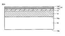
図24を参照して、本実施の形態の半導体発光素子1の製造方法は、ウエハ10の第1の主面10a上に活性層13を形成すること(S2)を備える。具体的には、図26を参照して、ウエハ10の第1の主面10a上に、n型半導体層12、活性層13、およびp型半導体層14がこの順で堆積される。n型半導体層12、活性層13、およびp型半導体層14を含む半導体層は、有機金属化学気相成長法(MOCVD法)、有機金属気相成長法(MOVPE法)、分子線エピタキシー法(MBE法)、ハイドライド気相成長法(HVPE法)等の方法で堆積される。   Referring to FIG. 24, the method for manufacturing semiconductor light emitting element 1 of the present embodiment includes forming active layer 13 on first main surface 10a of wafer 10 (S2). Specifically, referring to FIG. 26, n-type semiconductor layer 12, active layer 13, and p-type semiconductor layer 14 are deposited in this order on first main surface 10a of wafer 10. A semiconductor layer including the n-type semiconductor layer 12, the active layer 13, and the p-type semiconductor layer 14 is formed by metal organic chemical vapor deposition (MOCVD), metal organic chemical vapor deposition (MOVPE), molecular beam epitaxy ( MBE method) and hydride vapor phase epitaxy method (HVPE method).

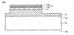
図27を参照して、n型半導体層12、活性層13、及びp型半導体層14を含む半導体層の一部を、エッチング等により部分的に除去し、メサ構造を形成する。n型半導体層12、活性層13、及びp型半導体層14を含む半導体層の一部を、エッチング等により部分的に除去することは、反応性イオンエッチング、誘導結合プラズマエッチング等のエッチングによって行ってもよい。エッチングによるダメージを除去するために、半導体層のエッチングされた面に、酸またはアルカリの溶液で表面処理を施すことが好ましい。   Referring to FIG. 27, a part of the semiconductor layer including n-type semiconductor layer 12, active layer 13, and p-type semiconductor layer 14 is partially removed by etching or the like to form a mesa structure. Part of the semiconductor layer including the n-type semiconductor layer 12, the active layer 13, and the p-type semiconductor layer 14 is partially removed by etching or the like by etching such as reactive ion etching or inductively coupled plasma etching. May be. In order to remove the damage caused by etching, it is preferable to perform a surface treatment on the etched surface of the semiconductor layer with an acid or alkali solution.

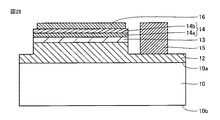
図28を参照して、n型半導体層12上にn型電極15を形成し、p型半導体層14上にp型電極16を形成する。特定的には、n型電極15を形成した後に、p型電極16を形成してもよい。   Referring to FIG. 28, n-type electrode 15 is formed on n-type semiconductor layer 12, and p-type electrode 16 is formed on p-type semiconductor layer 14. Specifically, the p-type electrode 16 may be formed after the n-type electrode 15 is formed.

n型電極15及びp型電極16のパターンニングは、リフトオフ法を用いて実施してもよい。具体的には、電極を形成する面にフォトレジストを塗布した後、紫外線をフォトレジストに部分的に照射する。その後、現像液にフォトレジストを浸漬させて、感光したフォトレジストを溶解させることにより所望のパターンのレジスト膜を形成する。パターニングされたレジスト膜上に電極となるべき金属膜を堆積させる。剥離液でレジスト膜を溶解し、レジスト膜上に位置していた金属膜を除去することにより、レジスト膜が形成されていない領域に位置する金属膜を残存させて所定のパターンを有する金属膜(電極)を形成する。   The patterning of the n-type electrode 15 and the p-type electrode 16 may be performed using a lift-off method. Specifically, after applying a photoresist to the surface on which the electrode is to be formed, the photoresist is partially irradiated with ultraviolet rays. Thereafter, a photoresist is immersed in the developer, and the exposed photoresist is dissolved to form a resist film having a desired pattern. A metal film to be an electrode is deposited on the patterned resist film. The resist film is dissolved with a stripping solution, and the metal film located on the resist film is removed, thereby leaving the metal film located in the region where the resist film is not formed and the metal film having a predetermined pattern ( Electrode).

電極をパターンニングする方法として、さらに以下の別の方法を例示することができる。電極を形成しようとする面(たとえばn型半導体層12の露出面)に電極となるべき金属膜を形成する。金属膜上にフォトレジストを塗布後、露光、現像工程を経てフォトレジストをパターニングする。その後、上記パターニングされたフォトレジスト(レジスト膜)をマスクとして用いて、金属膜にドライエッチングまたはウェットエッチングを施して、金属膜を部分的に除去する。その後、剥離液でフォトレジストを溶解する。   As a method for patterning the electrode, another method described below can be exemplified. A metal film to be an electrode is formed on the surface on which the electrode is to be formed (for example, the exposed surface of the n-type semiconductor layer 12). After applying a photoresist on the metal film, the photoresist is patterned through an exposure and development process. Thereafter, using the patterned photoresist (resist film) as a mask, the metal film is dry etched or wet etched to partially remove the metal film. Thereafter, the photoresist is dissolved with a stripping solution.

n型電極15及びp型電極16を構成する金属膜を堆積する方法は、真空蒸着法、スパッタリング法、化学気相成長法などの方法を用いることができる。金属膜中の不純物を排除する観点から、真空蒸着法を用いることが好ましい。n型電極15となるべき金属膜を堆積後、n型半導体層12とn型電極15との電気的コンタクトを向上させるため、300℃以上1100℃以下の温度で、30秒以上3分以下の時間、アニールすることが好ましい。p型電極16となるべき金属膜を堆積後、p型半導体層14(第2のp型半導体層14b)との電気的コンタクトを向上させるため、200℃以上800℃以下の温度で、30秒以上3分以下の時間、アニールすることが好ましい。   As a method for depositing the metal film constituting the n-type electrode 15 and the p-type electrode 16, a method such as a vacuum deposition method, a sputtering method, or a chemical vapor deposition method can be used. From the viewpoint of eliminating impurities in the metal film, it is preferable to use a vacuum deposition method. After depositing the metal film to be the n-type electrode 15, in order to improve the electrical contact between the n-type semiconductor layer 12 and the n-type electrode 15, the temperature is from 300 ° C. to 1100 ° C. for 30 seconds to 3 minutes. It is preferable to anneal for a time. After depositing a metal film to be the p-type electrode 16, in order to improve electrical contact with the p-type semiconductor layer 14 (second p-type semiconductor layer 14b), the temperature is 200 ° C. or higher and 800 ° C. or lower for 30 seconds. Annealing is preferably performed for a time of 3 minutes or less.

図24を参照して、本実施の形態の半導体発光素子1の製造方法は、ウエハ10の光吸収係数α(cm-1)及びウエハ10の厚さt(μm)が、340exp(−0.16α)≦t≦3200α-0.7を満たすように、ウエハ10の厚さtを定めること(S3)を備える。ウエハ10の厚さtは、ウエハ10の第1の主面10aと第2の主面10bとの最短距離で定義される。具体的には、ウエハ10の厚さを測定する。ウエハ10の厚さt(μm)と、ウエハ10の光吸収係数α(cm-1)とが、340exp(−0.16α)≦t≦3200α-0.7を満たす場合には、ウエハ10を研磨しないでそのまま用いる。ウエハ10の厚さt(μm)と、ウエハ10の光吸収係数α(cm-1)とが、340exp(−0.16α)≦t≦3200α-0.7を満たさない場合には、ウエハ10の光吸収係数α(cm-1)及びウエハ10の厚さt(μm)が、340exp(−0.16α)≦t≦3200α-0.7を満たすように、ウエハ10の厚さを薄くしてもよい(図29を参照)。ウエハ10の厚みを薄くする方法として、化学的機械研磨(CMP)を例示することができる。本実施の形態において、ウエハ10の厚さtを定めることは、ウエハ10を研磨しないでそのまま用いることと、ウエハ10の厚さを薄くすることの両者を含む。 Referring to FIG. 24, in the method for manufacturing semiconductor light emitting device 1 of the present embodiment, the light absorption coefficient α (cm −1 ) of wafer 10 and the thickness t (μm) of wafer 10 are 340 exp (−0. 16α) ≦ t ≦ 3200α −0.7 so as to satisfy the thickness t of the wafer 10 (S3). The thickness t of the wafer 10 is defined by the shortest distance between the first main surface 10a and the second main surface 10b of the wafer 10. Specifically, the thickness of the wafer 10 is measured. When the thickness t (μm) of the wafer 10 and the light absorption coefficient α (cm −1 ) of the wafer 10 satisfy 340exp (−0.16α) ≦ t ≦ 3200α− 0.7 , the wafer 10 is not polished. Use as is. When the thickness t (μm) of the wafer 10 and the light absorption coefficient α (cm −1 ) of the wafer 10 do not satisfy 340 exp (−0.16 α) ≦ t ≦ 3200 α −0.7 , the light of the wafer 10 The thickness of the wafer 10 may be reduced so that the absorption coefficient α (cm −1 ) and the thickness t (μm) of the wafer 10 satisfy 340exp (−0.16α) ≦ t ≦ 3200α −0.7 ( (See FIG. 29). An example of a method for reducing the thickness of the wafer 10 is chemical mechanical polishing (CMP). In the present embodiment, determining the thickness t of the wafer 10 includes both using the wafer 10 as it is without polishing and reducing the thickness of the wafer 10.

図24を参照して、本実施の形態の半導体発光素子1の製造方法は、ウエハ10を、複数の基板11に分割すること(S5)を備える。複数の基板11のそれぞれは、活性層13が形成された第1の主面11aと、第1の主面11aと反対側の第2の主面11bと、第1の主面11aと第2の主面11bとの間に延在する側面11cとを有する。基板11の第1の主面11a及び第2の主面11bは、それぞれ、ウエハ10の第1の主面10a及び第2の主面10bに対応する。図24を参照して、本実施の形態の半導体発光素子1の製造方法は、基板11の第1の主面11aと基板11の少なくとも一部の側面11cとがなす角βの補角θが、20°以上70°以下、または、100°以上140°以下になるように、基板11の少なくとも一部の側面11cを加工すること(S6)をさらに備える。基板11の少なくとも一部の側面11cを加工することは、ウエハ10を複数の基板11に分割した後に、基板11の側面をエッチング、研磨または研削することを含んでもよい。   Referring to FIG. 24, the method for manufacturing semiconductor light emitting element 1 of the present embodiment includes dividing wafer 10 into a plurality of substrates 11 (S5). Each of the plurality of substrates 11 includes a first main surface 11a on which an active layer 13 is formed, a second main surface 11b opposite to the first main surface 11a, a first main surface 11a, and a second main surface 11a. And a side surface 11c extending between the main surface 11b. The first main surface 11a and the second main surface 11b of the substrate 11 correspond to the first main surface 10a and the second main surface 10b of the wafer 10, respectively. Referring to FIG. 24, in the method of manufacturing semiconductor light emitting device 1 of the present embodiment, the complementary angle θ of angle β formed by first main surface 11a of substrate 11 and at least a part of side surface 11c of substrate 11 is , Further processing (S6) at least a part of the side surface 11c of the substrate 11 so as to be 20 ° to 70 °, or 100 ° to 140 °. Processing at least a portion of the side surface 11 c of the substrate 11 may include etching, polishing, or grinding the side surface of the substrate 11 after dividing the wafer 10 into the plurality of substrates 11.

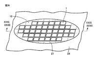
ウエハ10を複数の基板11に分割する際に、基板11の少なくとも一部の側面11cを加工してもよい。すなわち、ウエハ10を、複数の基板11に分割すること(S5)と、基板11の少なくとも一部の側面11cを加工すること(S6)とを、一つの工程で行ってもよい。具体的には、図30を参照して、活性層13等を含む半導体層が形成されたウエハ10をダイシングテープ24上に貼着する。ウエハ10にダイシングライン27を形成する。図31及び図32を参照して、ダイシングライン27に沿ってブレード37を動かして、ウエハ10を複数の半導体発光素子1に分割するとともに(S5)、基板11の少なくとも一部の側面11cを加工する(S6)。基板11の少なくとも一部の側面11cを加工することは、先端にテーパ部を有するブレードを用いることを含んでもよい(図31及び図32を参照)。ブレード37として、ダイヤモンドブレードを用いてもよい。   When the wafer 10 is divided into a plurality of substrates 11, at least a part of the side surface 11c of the substrate 11 may be processed. That is, the wafer 10 may be divided into a plurality of substrates 11 (S5) and at least a part of the side surface 11c of the substrate 11 may be processed (S6) in one step. Specifically, referring to FIG. 30, wafer 10 on which a semiconductor layer including active layer 13 and the like is formed is attached onto dicing tape 24. A dicing line 27 is formed on the wafer 10. Referring to FIGS. 31 and 32, the blade 37 is moved along the dicing line 27 to divide the wafer 10 into a plurality of semiconductor light emitting devices 1 (S5) and process at least a part of the side surface 11c of the substrate 11. (S6). Processing at least a portion of the side surface 11c of the substrate 11 may include using a blade having a tapered portion at the tip (see FIGS. 31 and 32). A diamond blade may be used as the blade 37.

図31を参照して、90°より小さい補角θを有する半導体発光素子1を製造する場合、活性層13等を含む半導体層が形成されたウエハ10のウエハ10側をダイシングテープ24に貼着する。先端にテーパ部37aを有するブレード37を用いてウエハ10を複数の半導体発光素子1に分割することによって、基板11の側面11cを、基板11の第1の主面11aに対して補角θで傾斜させることができる。こうして、基板11の第1の主面11aと側面11cとがなす角βの補角θを90°未満とすることができる。より特定的には、基板11の第1の主面11aと側面11cとがなす角βの補角θを、20°以上70°以下、好ましくは、20°以上60°以下、30°以上60°以下としてもよい。半導体発光素子1をダイシングテープ24から剥離することによって、半導体発光素子1を得ることができる。   Referring to FIG. 31, when manufacturing semiconductor light emitting element 1 having a complementary angle θ smaller than 90 °, wafer 10 side of wafer 10 on which a semiconductor layer including active layer 13 and the like is formed is attached to dicing tape 24. To do. By dividing the wafer 10 into a plurality of semiconductor light emitting devices 1 using a blade 37 having a tapered portion 37a at the tip, the side surface 11c of the substrate 11 is at a complementary angle θ with respect to the first main surface 11a of the substrate 11. Can be tilted. In this way, the complementary angle θ of the angle β formed by the first main surface 11a and the side surface 11c of the substrate 11 can be less than 90 °. More specifically, the complementary angle θ of the angle β formed by the first main surface 11a and the side surface 11c of the substrate 11 is 20 ° or more and 70 ° or less, preferably 20 ° or more and 60 ° or less, and 30 ° or more and 60 °. It may be less than °. The semiconductor light emitting element 1 can be obtained by peeling the semiconductor light emitting element 1 from the dicing tape 24.

図32を参照して、90°より大きい補角θを有する半導体発光素子1を製造する場合、活性層13等を含む半導体層が形成されたウエハ10の半導体層側をダイシングテープ24に貼着する。先端にテーパ部37aを有するブレード37を用いてウエハ10を複数の半導体発光素子1に分割することによって、基板11の側面11cを、基板11の第1の主面11aに対して補角θで傾斜させることができる。こうして、基板11の第1の主面11aと側面11cとがなす角βの補角θを90°より大きくすることができる。より特定的には、基板11の第1の主面11aと側面11cとがなす角βの補角θを、100°以上140°以下、好ましくは、110°以上140°以下としてもよい。半導体発光素子1をダイシングテープ24から剥離することによって、半導体発光素子1を得ることができる。   Referring to FIG. 32, when manufacturing semiconductor light emitting device 1 having a complementary angle θ greater than 90 °, the semiconductor layer side of wafer 10 on which a semiconductor layer including active layer 13 and the like is formed is attached to dicing tape 24. To do. By dividing the wafer 10 into a plurality of semiconductor light emitting devices 1 using a blade 37 having a tapered portion 37a at the tip, the side surface 11c of the substrate 11 is at a complementary angle θ with respect to the first main surface 11a of the substrate 11. Can be tilted. Thus, the complementary angle θ of the angle β formed by the first main surface 11a and the side surface 11c of the substrate 11 can be made larger than 90 °. More specifically, the complementary angle θ of the angle β formed by the first main surface 11a and the side surface 11c of the substrate 11 may be 100 ° to 140 °, preferably 110 ° to 140 °. The semiconductor light emitting element 1 can be obtained by peeling the semiconductor light emitting element 1 from the dicing tape 24.

本実施の形態の第1の変形例の半導体発光素子1aでは、図33(A)及び(B)に示すように、基板11の側面11cは、補角θの大きさが異なる複数の部分(第1の部分11c1、第2の部分11c2)を含んでもよい。基板11の第1の主面11aと側面11cの第1の部分11c1とがなす角β1の補角θ1は、基板11の第1の主面11aと側面11cの第2の部分11c2とがなす角β2の補角θ2と異なってもよい。本実施の形態の第1の変形例の半導体発光素子1aの製造方法では、基板11の少なくとも一部の側面11cを加工すること(S6)は、基板11の側面11cに、補角の大きさが異なる複数の部分(側面11cの第1の部分11c1、側面11cの第2の部分11c2)を形成することを含んでもよい。本実施の形態の第1の変形例では、基板11の第1の主面11aと側面11cの第1の部分11c1とがなす角β1の補角θ1と、基板11の第1の主面11aと側面11cの第2の部分11c2とがなす角β2の補角θ2とは、20°以上70°以下、または、100°以上140°以下である。基板11の側面11cが、補角θの大きさが異なる複数の部分(第1の部分11c1、第2の部分11c2)を含むため、半導体発光素子1の用途に応じて半導体発光素子1の配光特性等を変化させることができる。 In the semiconductor light emitting device 1a according to the first modification of the present embodiment, as shown in FIGS. 33A and 33B, the side surface 11c of the substrate 11 has a plurality of portions with different complementary angles θ ( The first portion 11c1 and the second portion 11c2) may be included. The complementary angle θ 1 of the angle β 1 formed by the first main surface 11a of the substrate 11 and the first portion 11c1 of the side surface 11c is the same as that of the first main surface 11a of the substrate 11 and the second portion 11c2 of the side surface 11c. There may be different from the supplementary angle θ 2 of the angle β 2. In the method for manufacturing the semiconductor light emitting device 1a according to the first modification of the present embodiment, the processing of at least a part of the side surface 11c of the substrate 11 (S6) Forming a plurality of different parts (a first part 11c1 of the side surface 11c and a second part 11c2 of the side surface 11c) may be included. In the first modification of the present embodiment, the complementary angle θ 1 of the angle β 1 formed by the first main surface 11a of the substrate 11 and the first portion 11c1 of the side surface 11c, and the first main surface of the substrate 11 The complementary angle θ 2 of the angle β 2 formed by the surface 11a and the second portion 11c2 of the side surface 11c is 20 ° or more and 70 ° or less, or 100 ° or more and 140 ° or less. Since the side surface 11 c of the substrate 11 includes a plurality of portions (first portion 11 c 1 and second portion 11 c 2) having different complementary angles θ, the arrangement of the semiconductor light emitting device 1 according to the use of the semiconductor light emitting device 1. Optical characteristics and the like can be changed.

本実施の形態の第2の変形例の半導体発光素子1bでは、図34(A)及び(B)に示すように、基板11の側面11cの周方向において基板11の一部の側面11c(側面11cの第1の部分11c1)が、基板11の第1の主面11aに対して、20°以上70°以下、または、100°以上140°以下の補角で傾斜してもよい。基板11の第1の主面11aと側面11cの第1の部分11c1とがなす角β1の補角θ1は、20°以上70°以下、または、100°以上140°以下であるが、基板11の第1の主面11aと側面11cの第2の部分11c3とがなす角β2の補角θ2は、20°未満、70°より大きく100°未満、または、140°より大きくてもよい。基板11の第1の主面11aと側面11cの第1の部分11c1とがなす角β1の補角θ1は、20°以上70°以下、または、100°以上140°以下であるが、基板11の第1の主面11aと側面11cの第2の部分11c3とがなす角β2と、角β2の補角θ2とは90°であり、基板11の第1の主面11aに対して傾斜していなくてもよい。基板11の第1の主面11aと少なくとも一部の側面11c(側面11cの第1の部分11c1)とがなす角の補角θ1は、20°以上70°以下、または、100°以上140°以下であるため、本実施の形態と同様の効果が得られる。 In the semiconductor light emitting device 1b according to the second modification of the present embodiment, as shown in FIGS. 34A and 34B, a part of the side surface 11c (side surface) of the substrate 11 in the circumferential direction of the side surface 11c of the substrate 11 is used. The first portion 11c1) of 11c may be inclined with respect to the first main surface 11a of the substrate 11 at a complementary angle of 20 ° to 70 °, or 100 ° to 140 °. The complementary angle θ 1 of the angle β 1 formed by the first main surface 11a of the substrate 11 and the first portion 11c1 of the side surface 11c is 20 ° or more and 70 ° or less, or 100 ° or more and 140 ° or less. The complementary angle θ 2 of the angle β 2 formed by the first main surface 11a of the substrate 11 and the second portion 11c3 of the side surface 11c is less than 20 °, more than 70 ° and less than 100 °, or more than 140 °. Also good. The complementary angle θ 1 of the angle β 1 formed by the first main surface 11a of the substrate 11 and the first portion 11c1 of the side surface 11c is 20 ° or more and 70 ° or less, or 100 ° or more and 140 ° or less. The angle β 2 formed by the first main surface 11a of the substrate 11 and the second portion 11c3 of the side surface 11c and the complementary angle θ 2 of the angle β 2 are 90 °, and the first main surface 11a of the substrate 11 May not be inclined. The complementary angle θ 1 of the angle formed by the first main surface 11a of the substrate 11 and at least a part of the side surface 11c (the first portion 11c1 of the side surface 11c) is 20 ° or more and 70 ° or less, or 100 ° or more 140. Since it is less than or equal to °, the same effect as the present embodiment can be obtained.

本実施の形態の第3の変形例の半導体発光素子1cでは、図35(A)及び(B)に示すように、基板11の厚さ方向において基板11の一部の側面11c(側面11cの第1の部分11c1)が、基板11の第1の主面11aに対して、20°以上70°以下、または、100°以上140°以下の補角で傾斜してもよい。基板11の第1の主面11aと側面11cの第1の部分11c1とがなす角β1の補角θ1は、20°以上70°以下、または、100°以上140°以下であるが、基板11の第1の主面11aと側面11cの第2の部分11c3とがなす角β2の補角θ2は、20°未満、70°より大きく100°未満、または、140°より大きくてもよい。基板11の第1の主面11aと側面11cの第1の部分11c1とがなす角β1の補角θ1は、20°以上70°以下、または、100°以上140°以下であるが、基板11の第1の主面11aと側面11cの第2の部分11c3とがなす角β2と、角β2の補角θ2とは90°であり、基板11の第1の主面11aに対して傾斜していなくてもよい。基板11の第1の主面11aと少なくとも一部の側面11c(側面11cの第1の部分11c1)とがなす角の補角θ1は、20°以上70°以下、または、100°以上140°以下であるため、本実施の形態と同様の効果が得られる。 In the semiconductor light emitting device 1c according to the third modification of the present embodiment, as shown in FIGS. 35A and 35B, a part of the side surface 11c of the substrate 11 in the thickness direction of the substrate 11 (of the side surface 11c). The first portion 11c1) may be inclined with respect to the first main surface 11a of the substrate 11 at a complementary angle of 20 ° to 70 °, or 100 ° to 140 °. The complementary angle θ 1 of the angle β 1 formed by the first main surface 11a of the substrate 11 and the first portion 11c1 of the side surface 11c is 20 ° or more and 70 ° or less, or 100 ° or more and 140 ° or less. The complementary angle θ 2 of the angle β 2 formed by the first main surface 11a of the substrate 11 and the second portion 11c3 of the side surface 11c is less than 20 °, more than 70 ° and less than 100 °, or more than 140 °. Also good. The complementary angle θ 1 of the angle β 1 formed by the first main surface 11a of the substrate 11 and the first portion 11c1 of the side surface 11c is 20 ° or more and 70 ° or less, or 100 ° or more and 140 ° or less. The angle β 2 formed by the first main surface 11a of the substrate 11 and the second portion 11c3 of the side surface 11c and the complementary angle θ 2 of the angle β 2 are 90 °, and the first main surface 11a of the substrate 11 May not be inclined. The complementary angle θ 1 of the angle formed by the first main surface 11a of the substrate 11 and at least a part of the side surface 11c (the first portion 11c1 of the side surface 11c) is 20 ° or more and 70 ° or less, or 100 ° or more 140. Since it is less than or equal to °, the same effect as the present embodiment can be obtained.

本実施の形態(第1の変形例から第3の変形例を含む)に係る半導体発光素子1及びその製造方法の効果を説明する。   The effects of the semiconductor light emitting element 1 and the method for manufacturing the same according to the present embodiment (including the first to third modifications) will be described.

本実施の形態の半導体発光素子1では、基板11の第1の主面11aと少なくとも一部の側面11cとがなす角βの補角θは、20°以上70°以下、または、100°以上140°以下である。基板11の光吸収係数α(cm-1)及び基板11の厚さt(μm)は、340exp(−0.16α)≦t≦3200α-0.7を満たす。本実施の形態の半導体発光素子1の製造方法は、ウエハ10の光吸収係数α(cm-1)及びウエハ10の厚さt(μm)が、340exp(−0.16α)≦t≦3200α-0.7を満たすように、ウエハ10の厚さtを定めること(S3)と、ウエハ10を、複数の基板11に分割することと、基板11の第1の主面11aと基板11の少なくとも一部の側面11cとがなす角βの補角θが、20°以上70°以下、または、100°以上140°以下になるように、基板11の少なくとも一部の側面11cを加工すること(S6)を備える。そのため、本実施の形態の半導体発光素子1及びその製造方法によれば、向上した光取り出し効率を有する、深紫外光を放射する半導体発光素子及びその製造方法を提供することができる。 In the semiconductor light emitting device 1 of the present embodiment, the complementary angle θ of the angle β formed by the first main surface 11a of the substrate 11 and at least a part of the side surface 11c is 20 ° or more and 70 ° or less, or 100 ° or more. 140 ° or less. The light absorption coefficient α (cm −1 ) of the substrate 11 and the thickness t (μm) of the substrate 11 satisfy 340exp (−0.16α) ≦ t ≦ 3200α− 0.7 . In the manufacturing method of the semiconductor light emitting device 1 of the present embodiment, the light absorption coefficient α (cm −1 ) of the wafer 10 and the thickness t (μm) of the wafer 10 are 340 exp (−0.16 α) ≦ t ≦ 3200 α −. The thickness t of the wafer 10 is determined so as to satisfy 0.7 (S3), the wafer 10 is divided into a plurality of substrates 11, the first main surface 11a of the substrate 11 and at least a part of the substrate 11 Processing at least a part of the side surface 11c of the substrate 11 so that the complementary angle θ of the angle β formed by the side surface 11c of the substrate 11 is 20 ° or more and 70 ° or less or 100 ° or more and 140 ° or less (S6). Is provided. Therefore, according to the semiconductor light emitting device 1 and the manufacturing method thereof of the present embodiment, it is possible to provide a semiconductor light emitting device that emits deep ultraviolet light having improved light extraction efficiency and a manufacturing method thereof.

基板11の側面11cは、補角θの大きさが異なる複数の部分(側面11cの第1の部分11c1、側面11cの第2の部分11c2)を含んでもよい。基板11の側面11cが、補角θの大きさが異なる複数の部分(側面11cの第1の部分11c1、側面11cの第2の部分11c2)を含むため、半導体発光素子1の用途に応じて半導体発光素子1の配光特性等を変化させることができる。   The side surface 11c of the substrate 11 may include a plurality of portions (a first portion 11c1 of the side surface 11c and a second portion 11c2 of the side surface 11c) having different magnitudes of the complementary angle θ. Since the side surface 11c of the substrate 11 includes a plurality of portions (first portion 11c1 of the side surface 11c, second portion 11c2 of the side surface 11c) having different magnitudes of the complementary angle θ, depending on the use of the semiconductor light emitting element 1 The light distribution characteristics and the like of the semiconductor light emitting element 1 can be changed.

(実施の形態2)
図36及び図37を参照して、実施の形態2に係る半導体発光素子2を説明する。本実施の形態の半導体発光素子2は、基本的には、図1及び図2に示す実施の形態1の半導体発光素子1と同様の構成を備え、同様の効果を得ることができるが、主に以下の点で異なる。
(Embodiment 2)
With reference to FIGS. 36 and 37, the semiconductor light emitting element 2 according to the second embodiment will be described. The semiconductor light emitting device 2 of the present embodiment basically has the same configuration as the semiconductor light emitting device 1 of the first embodiment shown in FIGS. 1 and 2 and can obtain the same effects. It differs in the following points.

本実施の形態の半導体発光素子2は、活性層13から放射される深紫外光を半導体発光素子2の外部に取り出す効率を向上させる凹凸構造17を含む。図36は、90°より小さい補角θを有する半導体発光素子2を示す。図37は、90°より大きい補角θを有する半導体発光素子2を示す。より具体的には、深紫外光を半導体発光素子2の外部に取り出す効率を向上させる凹凸構造17は、半導体発光素子2の出射面(第2の主面11b)に含まれてもよい。凹凸構造17は、半導体発光素子2の出射面(第2の主面11b)において、活性層13から放射される深紫外光が全反射されることを低減する。そのため、半導体発光素子2に凹凸構造17を設けることによって、半導体発光素子2の外部に深紫外光を取り出す効率を向上させることができる。   The semiconductor light emitting device 2 of the present embodiment includes a concavo-convex structure 17 that improves the efficiency of extracting deep ultraviolet light emitted from the active layer 13 to the outside of the semiconductor light emitting device 2. FIG. 36 shows the semiconductor light emitting device 2 having a complementary angle θ smaller than 90 °. FIG. 37 shows the semiconductor light emitting device 2 having a complementary angle θ greater than 90 °. More specifically, the concavo-convex structure 17 that improves the efficiency of extracting deep ultraviolet light to the outside of the semiconductor light emitting element 2 may be included in the emission surface (second main surface 11 b) of the semiconductor light emitting element 2. The uneven structure 17 reduces the total reflection of deep ultraviolet light emitted from the active layer 13 on the emission surface (second main surface 11b) of the semiconductor light emitting device 2. Therefore, providing the semiconductor light emitting element 2 with the concavo-convex structure 17 can improve the efficiency of extracting deep ultraviolet light outside the semiconductor light emitting element 2.

凹凸構造17は、凹部と凸部とがランダムに配列されてもよい。凹凸構造17は、凹部と凸部とが周期的に配列されてもよい。凹凸構造17は、三角格子、正方格子、または六方格子で配列されてもよい。凹凸構造17は、フィリングファクターが最大となる三角格子で配列されることが好ましい。凹凸構造17の凹部または凸部の形状は、角柱、円柱、円錐、角錐、球または半楕円球の形状を有してもよい。凹凸構造17は、フォトニック結晶構造を含んでもよい。   In the concavo-convex structure 17, concave portions and convex portions may be arranged at random. In the concavo-convex structure 17, concave portions and convex portions may be periodically arranged. The uneven structure 17 may be arranged in a triangular lattice, a square lattice, or a hexagonal lattice. The concavo-convex structure 17 is preferably arranged in a triangular lattice with a maximum filling factor. The shape of the concave portion or the convex portion of the concavo-convex structure 17 may have a shape of a prism, a cylinder, a cone, a pyramid, a sphere, or a semi-elliptical sphere. The uneven structure 17 may include a photonic crystal structure.

本実施の形態に係る半導体発光素子2の製造方法を説明する。本実施の形態に係る半導体発光素子2の製造方法の一例は、図24から図32に示される製造方法と基本的に同じであるが、ウエハ10の第2の主面10bに、半導体発光素子2の活性層13から放射される深紫外光を半導体発光素子2の外部に取り出す効率を向上させる凹凸構造17を形成すること(S4)をさらに備える(図38を参照)。より特定的には、n型電極15及びp型電極16を形成した後、かつ、ウエハ10を複数の基板11に分割する前に、ウエハ10の第1の主面10aと反対側の第2の主面10bに、半導体発光素子2の活性層13から放射される深紫外光を半導体発光素子2の外部に取り出す効率を向上させる凹凸構造17を形成することを含む。   A method for manufacturing the semiconductor light emitting device 2 according to the present embodiment will be described. An example of the manufacturing method of the semiconductor light emitting device 2 according to the present embodiment is basically the same as the manufacturing method shown in FIGS. 24 to 32, but the semiconductor light emitting device is formed on the second main surface 10 b of the wafer 10. And forming a concavo-convex structure 17 that improves the efficiency of extracting deep ultraviolet light emitted from the active layer 13 to the outside of the semiconductor light emitting element 2 (see FIG. 38). More specifically, after the n-type electrode 15 and the p-type electrode 16 are formed and before the wafer 10 is divided into a plurality of substrates 11, a second second side opposite to the first major surface 10 a of the wafer 10. Forming a concavo-convex structure 17 for improving the efficiency of extracting deep ultraviolet light emitted from the active layer 13 of the semiconductor light emitting device 2 to the outside of the semiconductor light emitting device 2.

ウエハ10の第2の主面10bに凹凸構造17を形成することは、ウエハ10の第2の主面10bにパターニングされたマスクを形成することと、パターニングされたマスクを用いてウエハ10の第2の主面10bをエッチングすることとを含んでもよい。ウエハ10の第2の主面10bをエッチングすることは、誘導結合プラズマ(ICP)エッチング、もしくは反応性イオンエッチング(RIE)等のドライエッチング、または酸性溶液、もしくはアルカリ性溶液をエッチング液として用いるウェットエッチングなどによって行ってもよい。それから、ウエハ10をダイシングして、個片化された半導体発光素子2が得られる。   Forming the concavo-convex structure 17 on the second main surface 10b of the wafer 10 includes forming a patterned mask on the second main surface 10b of the wafer 10 and using the patterned mask. Etching the second main surface 10b. Etching the second main surface 10b of the wafer 10 includes dry etching such as inductively coupled plasma (ICP) etching or reactive ion etching (RIE), or wet etching using an acidic solution or an alkaline solution as an etching solution. Etc. may be performed. Then, the wafer 10 is diced to obtain the separated semiconductor light emitting device 2.

本実施の形態の半導体発光素子2及びその製造方法は、実施の形態1の半導体発光素子1及びその製造方法が有する作用及び効果に加えて、以下の作用及び効果を説明する。   The semiconductor light emitting element 2 and the manufacturing method thereof according to the present embodiment will be described in addition to the functions and effects of the semiconductor light emitting element 1 and the manufacturing method thereof according to the first embodiment.

凹凸構造17は、深紫外光の出射面である半導体発光素子2の第2の主面11bにおいて、半導体発光素子2の活性層13から放射される深紫外光が全反射されることを低減する。そのため、凹凸構造17は、半導体発光素子2の外部に深紫外光を取り出す効率を向上させることができる。本実施の形態の半導体発光素子2及びその製造方法によれば、さらに向上した光取り出し効率を有する、深紫外光を放射する半導体発光素子及びその製造方法を提供することができる。   The concavo-convex structure 17 reduces the total reflection of deep ultraviolet light emitted from the active layer 13 of the semiconductor light emitting element 2 on the second main surface 11b of the semiconductor light emitting element 2 that is the emission surface of the deep ultraviolet light. . Therefore, the concavo-convex structure 17 can improve the efficiency of extracting deep ultraviolet light to the outside of the semiconductor light emitting element 2. According to the semiconductor light emitting device 2 and the manufacturing method thereof of the present embodiment, it is possible to provide a semiconductor light emitting device that emits deep ultraviolet light and has a further improved light extraction efficiency and a manufacturing method thereof.

(実施の形態3)
図39を参照して、実施の形態3に係る発光モジュール5を説明する。
(Embodiment 3)
With reference to FIG. 39, the light emitting module 5 which concerns on Embodiment 3 is demonstrated.

図39を参照して、実施の形態3に係る発光モジュール5は、主に、深紫外光を放射する半導体発光素子1と、半導体発光素子1を支持する支持部材(30)と、半導体発光素子1を収容するパッケージ(30,40,44)とを備える。パッケージ(30,40,44)は、基台30と、透明部材40と、キャップ44とを含んでもよい。   Referring to FIG. 39, light emitting module 5 according to Embodiment 3 mainly includes semiconductor light emitting element 1 that emits deep ultraviolet light, a support member (30) that supports semiconductor light emitting element 1, and the semiconductor light emitting element. 1 (30, 40, 44). The package (30, 40, 44) may include a base 30, a transparent member 40, and a cap 44.

基台30は、半導体発光素子1を支持する。半導体発光素子1は、基台30上にフリップチップボンディングされている。本実施の形態の発光モジュール5では、図2に示される90°より大きい補角θを有する半導体発光素子1が用いられている。本実施の形態における半導体発光素子1は、第1の主面11aと、第1の主面11aと反対側の第2の主面11bと、第1の主面11aと第2の主面11bとの間に延在する側面11cとを有する基板11と、基板11の第1の主面11a上に設けられた活性層13とを備える。基板11の第1の主面11aと少なくとも一部の側面11cとがなす角βの補角θは、100°以上140°以下である。   The base 30 supports the semiconductor light emitting element 1. The semiconductor light emitting element 1 is flip-chip bonded on the base 30. In the light emitting module 5 of the present embodiment, the semiconductor light emitting element 1 having a complementary angle θ larger than 90 ° shown in FIG. 2 is used. The semiconductor light emitting device 1 in the present embodiment includes a first main surface 11a, a second main surface 11b opposite to the first main surface 11a, a first main surface 11a, and a second main surface 11b. And a substrate 11 having a side surface 11c extending between and an active layer 13 provided on a first main surface 11a of the substrate 11. The complementary angle θ of the angle β formed by the first main surface 11a of the substrate 11 and at least a part of the side surface 11c is not less than 100 ° and not more than 140 °.

基台30に用いられる材料として、金属、樹脂、セラミックを例示することができる。本明細書において、金属で形成される基台30を含むパッケージ(30,40,44)をメタルパッケージと呼び、樹脂で形成される基台30を含むパッケージ(30,40,44)を樹脂パッケージと呼び、セラミックで形成される基台30を含むパッケージ(30,40,44)をセラミックパッケージと呼ぶ。本実施の形態のパッケージ(30,40,44)は、メタルパッケージ、樹脂パッケージ、セラミックパッケージのいずれかであってもよい。基台30は、高い熱伝導性を有する材料から構成され、ヒートシンクとして機能してもよい。   Examples of materials used for the base 30 include metals, resins, and ceramics. In this specification, a package (30, 40, 44) including a base 30 formed of metal is referred to as a metal package, and a package (30, 40, 44) including a base 30 formed of resin is referred to as a resin package. The package (30, 40, 44) including the base 30 made of ceramic is called a ceramic package. The package (30, 40, 44) of the present embodiment may be a metal package, a resin package, or a ceramic package. The base 30 is made of a material having high thermal conductivity, and may function as a heat sink.

パッケージ(30,40,44)は、サブマウント20をさらに含んでもよい。本実施の形態では、基台30は、サブマウント20を介して、半導体発光素子1を支持する。サブマウント20は、半導体発光素子1を載置する。サブマウント20の材料として、窒化アルミニウム(AlN)、アルミナ(Al23)、炭化珪素(SiC)、ダイヤモンド、珪素(Si)を例示することができる。サブマウント20は、高い熱伝導性を有する材料から構成されることが好ましい。そのため、サブマウント20は、好ましくは、160〜250W/(m・K)の熱伝導率を有する窒化アルミニウム(AlN)から構成されてもよい。半導体発光素子1が載置されるサブマウントの表面は、平らな面であってもよいし、曲面であってもよい。半導体発光素子1が載置されるサブマウント20の表面に、半導体発光素子1が放射する深紫外光を反射するために、アルミニウム(Al)、チタン(Ti)、ニッケル(Ni)、金(Au)、または銀(Ag)などで形成される反射部材が設けられてもよい。 The package (30, 40, 44) may further include a submount 20. In the present embodiment, the base 30 supports the semiconductor light emitting element 1 via the submount 20. The submount 20 mounts the semiconductor light emitting element 1. Examples of the material of the submount 20 include aluminum nitride (AlN), alumina (Al 2 O 3 ), silicon carbide (SiC), diamond, and silicon (Si). The submount 20 is preferably made of a material having high thermal conductivity. Therefore, the submount 20 may be preferably made of aluminum nitride (AlN) having a thermal conductivity of 160 to 250 W / (m · K). The surface of the submount on which the semiconductor light emitting element 1 is placed may be a flat surface or a curved surface. In order to reflect the deep ultraviolet light emitted from the semiconductor light emitting element 1 on the surface of the submount 20 on which the semiconductor light emitting element 1 is mounted, aluminum (Al), titanium (Ti), nickel (Ni), gold (Au ), Or a reflective member formed of silver (Ag) or the like may be provided.

半導体発光素子1が載置されるサブマウント20の表面に、第1の導電パッド21と第2の導電パッド22とが設けられてもよい。導電性を有する接合部材25を用いて、半導体発光素子1のn型電極15とサブマウント20の第1の導電パッド21とが電気的及び機械的に接続され、半導体発光素子1のp型電極16とサブマウント20の第2の導電パッド22とが電気的及び機械的に接続される。接合部材25として、金−すず(AuSn)、銀−すず(AgSn)などからなる半田、金(Au)や銅(Cu)などからなる金属バンプ、銀ペーストなどの導電性ペーストを例示することができる。   A first conductive pad 21 and a second conductive pad 22 may be provided on the surface of the submount 20 on which the semiconductor light emitting element 1 is placed. Using the bonding member 25 having conductivity, the n-type electrode 15 of the semiconductor light-emitting element 1 and the first conductive pad 21 of the submount 20 are electrically and mechanically connected, and the p-type electrode of the semiconductor light-emitting element 1 is obtained. 16 and the second conductive pad 22 of the submount 20 are electrically and mechanically connected. Examples of the bonding member 25 include solder made of gold-tin (AuSn), silver-tin (AgSn), metal bumps made of gold (Au), copper (Cu), etc., and conductive paste such as silver paste. it can.

本実施の形態では、半導体発光素子1はサブマウント20の上にフリップチップボンディングされてもよい。すなわち、半導体発光素子1の基板11側の面をサブマウント20及び基台30と反対側に向けるとともに、半導体発光素子1の半導体層(n型半導体層12、活性層13、p型半導体層14)側の面をサブマウント20及び基台30の側に向けて、半導体発光素子1をサブマウント20の上に載置してもよい。半導体発光素子1がサブマウント20の上にフリップチップボンディングされると、活性層13から放射される深紫外光がp型半導体層14で吸収されることを抑制しながら、活性層13から放射される深紫外光を半導体発光素子1の外部に取り出すことができる。   In the present embodiment, the semiconductor light emitting element 1 may be flip-chip bonded on the submount 20. That is, the surface of the semiconductor light emitting element 1 on the substrate 11 side is directed to the side opposite to the submount 20 and the base 30, and the semiconductor layers of the semiconductor light emitting element 1 (n-type semiconductor layer 12, active layer 13, p-type semiconductor layer 14). The semiconductor light emitting element 1 may be mounted on the submount 20 with the surface on the side facing the submount 20 and the base 30. When the semiconductor light emitting device 1 is flip-chip bonded onto the submount 20, the deep ultraviolet light emitted from the active layer 13 is emitted from the active layer 13 while suppressing the absorption by the p-type semiconductor layer 14. Deep ultraviolet light can be taken out of the semiconductor light emitting device 1.

サブマウント20は、金−すず(AuSn)などからなる共晶半田、銀ペーストなどの導電性ペースト、または接着剤を用いて、基台30に固着される。半導体発光素子1から放射される深紫外光を効率的にパッケージ(30,40,44)の外部に取り出すために、半導体発光素子1は、基台30の主面30aの中央付近に載置されることが好ましい。   The submount 20 is fixed to the base 30 using eutectic solder made of gold-tin (AuSn) or the like, conductive paste such as silver paste, or an adhesive. In order to efficiently extract the deep ultraviolet light emitted from the semiconductor light emitting element 1 to the outside of the package (30, 40, 44), the semiconductor light emitting element 1 is placed near the center of the main surface 30a of the base 30. It is preferable.

本実施の形態のパッケージ(30,40,44)は、さらに、リードピン31と、導電ワイヤ33とを含んでもよい。リードピン31は基台30に固定されてもよい。導電ワイヤ33は、リードピン31と、第1の導電パッド21及び第2の導電パッド22とを電気的に接続する。導電ワイヤ33として、金(Au)ワイヤを例示することができる。リードピン31、第1の導電パッド21、第2の導電パッド22、接合部材25を介して、図示されない外部の電源から、半導体発光素子1に電流が供給され、半導体発光素子1は深紫外光を放射する。   The package (30, 40, 44) of the present embodiment may further include a lead pin 31 and a conductive wire 33. The lead pin 31 may be fixed to the base 30. The conductive wire 33 electrically connects the lead pin 31 to the first conductive pad 21 and the second conductive pad 22. As the conductive wire 33, a gold (Au) wire can be exemplified. A current is supplied to the semiconductor light emitting element 1 from an external power source (not shown) via the lead pin 31, the first conductive pad 21, the second conductive pad 22, and the bonding member 25. The semiconductor light emitting element 1 emits deep ultraviolet light. Radiate.

パッケージ(30,40,44)は、半導体発光素子1から放射される深紫外光に対して透明な透明部材40を有する。本実施の形態では、透明部材40は、平板である。透明部材40は、表面にレンズが形成された透明板であってもよい。このレンズによって、半導体発光素子1aから放射された深紫外光の配光特性を変化させることができる。透明部材40は、キャップ44によって機械的に支持されてもよい。キャップ44に用いられる材料として、金属または樹脂を例示することができる。キャップ44は、接着剤42または溶接等によって、基台30に固定されてもよい。   The package (30, 40, 44) includes a transparent member 40 that is transparent to deep ultraviolet light emitted from the semiconductor light emitting element 1. In the present embodiment, the transparent member 40 is a flat plate. The transparent member 40 may be a transparent plate having a lens formed on the surface. With this lens, it is possible to change the light distribution characteristics of deep ultraviolet light emitted from the semiconductor light emitting element 1a. The transparent member 40 may be mechanically supported by the cap 44. Examples of the material used for the cap 44 include metals and resins. The cap 44 may be fixed to the base 30 by an adhesive 42 or welding.

透明部材40は、半導体発光素子1から放射される深紫外光に対して透明である。本明細書において、透明部材40は、半導体発光素子1から放射される深紫外光に対して透明であるとは、透明部材40は、半導体発光素子1から放射される深紫外光の波長において、60%以上の透過率を有することを意味する。透明部材40は、半導体発光素子1から放射される深紫外光の波長において、好ましくは75%以上、さらに好ましくは90%以上の透過率を有してもよい。ここで、透明部材40の透過率は、単位長さ当たりの透明部材40の透過率が高いほど高くなり、透明部材40が厚いほど低くなる。透明部材40は、190nm以上350nm以下、好ましくは200nm以上320nm以下、さらに好ましくは220nm以上300nm以下の波長を有する深紫外光に対して低い光吸収係数と高い光透過率を有してもよい。透明部材40は、半導体発光素子1から放射される深紫外光の波長において、100μmの経路長当たり80%以上、好ましくは90%以上、さらに好ましくは95%以上の透過率を有する材料から構成されてもよい。   The transparent member 40 is transparent to deep ultraviolet light emitted from the semiconductor light emitting element 1. In the present specification, the transparent member 40 is transparent to the deep ultraviolet light emitted from the semiconductor light emitting element 1. The transparent member 40 is the wavelength of the deep ultraviolet light emitted from the semiconductor light emitting element 1. It means having a transmittance of 60% or more. The transparent member 40 may have a transmittance of preferably 75% or more, more preferably 90% or more at the wavelength of deep ultraviolet light emitted from the semiconductor light emitting device 1. Here, the transmittance of the transparent member 40 increases as the transmittance of the transparent member 40 per unit length increases, and decreases as the transparent member 40 increases in thickness. The transparent member 40 may have a low light absorption coefficient and a high light transmittance for deep ultraviolet light having a wavelength of 190 nm to 350 nm, preferably 200 nm to 320 nm, more preferably 220 nm to 300 nm. The transparent member 40 is made of a material having a transmittance of 80% or more, preferably 90% or more, more preferably 95% or more per 100 μm path length at the wavelength of deep ultraviolet light emitted from the semiconductor light emitting device 1. May be.

透明部材40は、合成石英、石英ガラス、無アルカリガラス、サファイア、蛍石(CaF)などの無機化合物、および樹脂のいずれかから構成されてもよい。   The transparent member 40 may be made of any one of an inorganic compound such as synthetic quartz, quartz glass, alkali-free glass, sapphire, and fluorite (CaF), and a resin.

透明部材40に用いることができる樹脂として、芳香族環を有しないシリコーン樹脂、非晶質のフッ素含有樹脂、ポリイミド、エポキシ樹脂、ポリオレフィン、ポリメタクリル酸メチルなどのアクリル樹脂、ポリカーボネート、ポリエステル、ポリウレタン、ポリスルホン系樹脂、ポリシラン、ポリビニルエーテル、無機化合物が添加された樹脂を例示することができる。   As a resin that can be used for the transparent member 40, a silicone resin having no aromatic ring, an amorphous fluorine-containing resin, a polyimide, an epoxy resin, a polyolefin, an acrylic resin such as polymethyl methacrylate, polycarbonate, polyester, polyurethane, Examples of the resin include a polysulfone resin, polysilane, polyvinyl ether, and an inorganic compound.

芳香環を有しないシリコーン樹脂として、ポリジメチルシロキサンであるJCR6122(東レ・ダウコーニング製)、JCR6140(東レ・ダウコーニング製)、HE59(日本山村硝子製)、HE60(日本山村硝子製)、HE61(日本山村硝子製)、KER2910(信越化学工業製)、含フッ素系オルガノポリシロキサンであるFER7061(信越化学工業製)を例示することができる。   As a silicone resin having no aromatic ring, polydimethylsiloxane JCR6122 (Toray Dow Corning), JCR6140 (Toray Dow Corning), HE59 (Nihon Yamamura Glass), HE60 (Nihon Yamamura Glass), HE61 ( Nihon Yamamura Glass Co., Ltd.), KER2910 (manufactured by Shin-Etsu Chemical Co., Ltd.), and fluorine-containing organopolysiloxane FER7061 (manufactured by Shin-Etsu Chemical Co., Ltd.).

非晶質のフッ素含有樹脂として、ペルフルオロ(4−ビニルオキシ−1−ブテン)重合体(サイトップ(登録商標)、旭硝子製)、2,2−ビストリフルオロメチル−4,5−ジフルオロ−1,3−ジオキソール重合体(テフロン(登録商標)AF、DuPont製)を例示することができる。   As an amorphous fluorine-containing resin, perfluoro (4-vinyloxy-1-butene) polymer (Cytop (registered trademark), manufactured by Asahi Glass), 2,2-bistrifluoromethyl-4,5-difluoro-1,3 -A dioxole polymer (Teflon (registered trademark) AF, manufactured by DuPont) can be exemplified.

ポリイミドとして、芳香族化合物が脂環式化合物に置換されたポリイミドが好ましい。脂環式ポリイミドとして、脂環式酸二無水物と脂環式ジアミンの反応物を例示することができる。脂環式酸二無水物として、ビシクロ[2.2.1]ヘプタ−2−endo,3−endo,5−exo,6−exo−テトラカルボン酸−2,3:5,6−二無水物、ビシクロ[2.2.1]ヘプタ−2−exo,3−exo,5−exo,6−exo−テトラカルボン酸−2,3:5,6−二無水物、ビシクロ[2.2.2]オクタ−2−endo,3−endo,5−exo,6−exo−テトラカルボン酸2,3:5,6−二無水物、ビシクロ[2.2.2]オクタ−2−exo,3−exo,5−exo,6−exo−テトラカルボン酸2,3:5,6−二無水物、(4arH,8acH)−デカヒドロ−1t,4t:5c,8c−ジメタノナフタレン2c,3c,6c,7c−テトラカルボン酸−2,3:6,7−二無水物を例示することができる。脂環式ジアミンとして、ビス(アミノメチルビシクロ[2.2.1]ヘプタンを例示することができる。   As the polyimide, a polyimide in which an aromatic compound is substituted with an alicyclic compound is preferable. Examples of the alicyclic polyimide include a reaction product of an alicyclic acid dianhydride and an alicyclic diamine. As an alicyclic acid dianhydride, bicyclo [2.2.1] hept-2-endo, 3-endo, 5-exo, 6-exo-tetracarboxylic acid-2, 3: 5,6-dianhydride , Bicyclo [2.2.1] hept-2-exo, 3-exo, 5-exo, 6-exo-tetracarboxylic acid-2,3: 5,6-dianhydride, bicyclo [2.2.2 ] Octa-2-endo, 3-endo, 5-exo, 6-exo-tetracarboxylic acid 2,3: 5,6-dianhydride, bicyclo [2.2.2] oct-2-exo, 3- exo, 5-exo, 6-exo-tetracarboxylic acid 2,3: 5,6-dianhydride, (4arH, 8acH) -decahydro-1t, 4t: 5c, 8c-dimethananaphthalene 2c, 3c, 6c, 7c-tetracarboxylic acid-2,3: 6,7-dianhydride can be exemplified. Examples of the alicyclic diamine include bis (aminomethylbicyclo [2.2.1] heptane.

エポキシ樹脂として、芳香環が脂環式化合物に変更されたエポキシ樹脂が好ましい。芳香環が脂環式化合物に変更されたエポキシ樹脂としては、3’,4’−エポキシシクロヘキシルメチル3,4−エポキシシクロヘキサンカルボキシレート(セロキサイド2021P,ダイセル製)、ε−カプロラクトン変性3’,4’−エポキシシクロヘキシルメチル3,4−エポキシシクロヘキサンカルボキシレート(セロキサイド2081,ダイセル製)、1,2−エポキシ−4−ビニルシクロヘキサン(セロキサイド2000,ダイセル製)を例示することができる。   As the epoxy resin, an epoxy resin in which the aromatic ring is changed to an alicyclic compound is preferable. Examples of the epoxy resin in which the aromatic ring is changed to an alicyclic compound include 3 ′, 4′-epoxycyclohexylmethyl 3,4-epoxycyclohexanecarboxylate (Celoxide 2021P, manufactured by Daicel), ε-caprolactone modified 3 ′, 4 ′. -Epoxycyclohexylmethyl 3,4-epoxycyclohexanecarboxylate (Celoxide 2081, manufactured by Daicel) and 1,2-epoxy-4-vinylcyclohexane (Celoxide 2000, manufactured by Daicel) can be exemplified.

ポリオレフィンとして、ポリエチレン、ポリプロピレン、メチルペンテンなどの鎖状オレフィンの重合体、ノルボルネンなどの環状オレフィンの重合体、TPX(三井化学製)、APEL(三井化学製)、ARTON(JSR製)、ZEONOR(日本ゼオン製)、ZEONEX(日本ゼオン製)、TOPAS(ポリプラスチックス製)を例示することができる。   As polyolefins, polymers of chain olefins such as polyethylene, polypropylene and methylpentene, polymers of cyclic olefins such as norbornene, TPX (made by Mitsui Chemicals), APEL (made by Mitsui Chemicals), ARTON (made by JSR), ZEONOR (Japan) Examples include Zeon), ZEONEX (Nippon Zeon), and TOPAS (Polyplastics).

無機化合物が添加された樹脂として、酸化マグネシウム、酸化ジルコニウム、酸化ホフニウム、α-酸化アルミニウム、γ-酸化アルミニウム、窒化アルミニウム、フッ化カルシウム、ルテチウムアルミニウムガーネット、二酸化ケイ素、マグネシウムアルミネート、サファイア、ダイヤモンドなどの無機化合物を、上記の樹脂に添加したものを例示することができる。   Resins with inorganic compounds added include magnesium oxide, zirconium oxide, hofnium oxide, α-aluminum oxide, γ-aluminum oxide, aluminum nitride, calcium fluoride, lutetium aluminum garnet, silicon dioxide, magnesium aluminate, sapphire, diamond, etc. The thing which added this inorganic compound to said resin can be illustrated.

本実施の形態に係る発光モジュール5の作用及び効果を説明する。
本実施の形態に係る発光モジュール5は、図2に示される半導体発光素子1と、半導体発光素子1を支持する支持部材(30)と、半導体発光素子1を収容するパッケージ(30,40,44)とを備える。パッケージ(30,40,44)は、半導体発光素子1から放射される光に対して透明な透明部材40を有する。本実施の形態の発光モジュール5によれば、向上した光取り出し効率を有する、深紫外光を放射する半導体発光素子1を備える発光モジュールを提供することができる。
The operation and effect of the light emitting module 5 according to the present embodiment will be described.
The light emitting module 5 according to the present embodiment includes a semiconductor light emitting element 1 shown in FIG. 2, a support member (30) that supports the semiconductor light emitting element 1, and packages (30, 40, 44) that house the semiconductor light emitting element 1. ). The package (30, 40, 44) includes a transparent member 40 that is transparent to the light emitted from the semiconductor light emitting element 1. According to the light emitting module 5 of the present embodiment, it is possible to provide a light emitting module including the semiconductor light emitting element 1 that emits deep ultraviolet light and has improved light extraction efficiency.

透明部材40は、半導体発光素子1から放射される深紫外光に対して透明であるので、透明部材40は、深紫外光の波長において、低い光吸収係数及び高い光透過率を有する。そのため、半導体発光素子1から放射される深紫外光をパッケージ(30,40,44)の外部へ効率よく取り出すことができる。さらに、透明部材40が深紫外光に長時間さらされても、深紫外光の波長における透明部材40の光透過率が低下することを防ぐことができる。その結果、本実施の形態の発光モジュール5によれば、向上した光取り出し効率を有する、深紫外光を放射する半導体発光素子1を備える、信頼性が高くかつ高い光出力を有する発光モジュールを提供することができる。   Since the transparent member 40 is transparent to the deep ultraviolet light emitted from the semiconductor light emitting element 1, the transparent member 40 has a low light absorption coefficient and a high light transmittance at the wavelength of the deep ultraviolet light. Therefore, deep ultraviolet light emitted from the semiconductor light emitting element 1 can be efficiently extracted outside the package (30, 40, 44). Furthermore, even if the transparent member 40 is exposed to deep ultraviolet light for a long time, the light transmittance of the transparent member 40 at the wavelength of deep ultraviolet light can be prevented from decreasing. As a result, according to the light emitting module 5 of the present embodiment, there is provided a light emitting module having improved light extraction efficiency and having a semiconductor light emitting element 1 that emits deep ultraviolet light and having high reliability and high light output. can do.

(実施の形態4)
図40を参照して、実施の形態4に係る発光モジュール5aを説明する。本実施の形態の発光モジュール5aは、基本的には、図39に示す実施の形態3の発光モジュール5と同様の構成を備え、同様の効果を得ることができるが、主に以下の点で異なる。本実施の形態に係る発光モジュール5aは、主に、深紫外光18を放射する半導体発光素子2と、半導体発光素子2を支持する支持部材(60)と、半導体発光素子2を収容するパッケージ(40、60)とを備える。
(Embodiment 4)
With reference to FIG. 40, the light emitting module 5a which concerns on Embodiment 4 is demonstrated. The light emitting module 5a of the present embodiment basically has the same configuration as the light emitting module 5 of the third embodiment shown in FIG. 39 and can obtain the same effects, but mainly in the following points. Different. The light emitting module 5a according to the present embodiment mainly includes a semiconductor light emitting element 2 that emits deep ultraviolet light 18, a support member (60) that supports the semiconductor light emitting element 2, and a package that houses the semiconductor light emitting element 2 ( 40, 60).

本実施の形態の発光モジュール5aでは、パッケージ(40、60)は、基台60と透明部材40とを含む。本実施の形態のパッケージ(40、60)は、実施の形態3の基台30に代えて、基台60を含む。基台60に用いられる材料として、金属、樹脂、セラミックを例示することができる。本明細書において、金属で形成される基台60を含むパッケージ(40、60)をメタルパッケージと呼び、樹脂で形成される基台60を含むパッケージ(40、60)を樹脂パッケージと呼び、セラミックで形成される基台60を含むパッケージ(40、60)をセラミックパッケージと呼ぶ。本実施の形態のパッケージ(40、60)は、メタルパッケージ、樹脂パッケージ、セラミックパッケージのいずれかであってもよい。基台60は、高い熱伝導性を有する材料から構成され、ヒートシンクとして機能してもよい。本実施の形態では、基台60の材料として、窒化アルミニウム(AlN)を用いてもよい。   In the light emitting module 5a of the present embodiment, the package (40, 60) includes a base 60 and a transparent member 40. The package (40, 60) of the present embodiment includes a base 60 in place of the base 30 of the third embodiment. Examples of materials used for the base 60 include metals, resins, and ceramics. In this specification, the package (40, 60) including the base 60 formed of metal is referred to as a metal package, and the package (40, 60) including the base 60 formed of resin is referred to as a resin package, and ceramic. The packages (40, 60) including the base 60 formed in the above are called ceramic packages. The package (40, 60) of the present embodiment may be a metal package, a resin package, or a ceramic package. The base 60 is made of a material having high thermal conductivity and may function as a heat sink. In the present embodiment, aluminum nitride (AlN) may be used as the material of the base 60.

基台60は、その周囲に側壁61が設けられている。透明部材40の周縁部は、基台60の側壁61の頂部に載置され、透明部材40は、基台60の側壁61によって、機械的に支持される。透明部材40は、接着剤42などを用いて、基台60の側壁61の上に固定される。   A side wall 61 is provided around the base 60. The peripheral edge of the transparent member 40 is placed on the top of the side wall 61 of the base 60, and the transparent member 40 is mechanically supported by the side wall 61 of the base 60. The transparent member 40 is fixed on the side wall 61 of the base 60 using an adhesive 42 or the like.

側壁61の内部には、半導体発光素子1を収容する凹部62が形成されている。基台30は、半導体発光素子1を載置する。基台60は半導体発光素子1を支持する。より特定的には、半導体発光素子1は、基台60の凹部62の底面64上にフリップチップボンディングされている。本実施の形態の発光モジュール5aでは、図1に示される90°より小さい補角θを有する半導体発光素子1が用いられている。本実施の形態における半導体発光素子1は、第1の主面11aと、第1の主面11aと反対側の第2の主面11bと、第1の主面11aと第2の主面11bとの間に延在する側面11cとを有する基板11と、基板11の第1の主面11a上に設けられた活性層13とを備える。基板11の第1の主面11aと少なくとも一部の側面11cとがなす角βの補角θは、20°以上70°以下である。   A recess 62 for accommodating the semiconductor light emitting element 1 is formed inside the side wall 61. The base 30 mounts the semiconductor light emitting element 1. The base 60 supports the semiconductor light emitting element 1. More specifically, the semiconductor light emitting element 1 is flip-chip bonded on the bottom surface 64 of the recess 62 of the base 60. In the light emitting module 5a of the present embodiment, the semiconductor light emitting element 1 having a complementary angle θ smaller than 90 ° shown in FIG. 1 is used. The semiconductor light emitting device 1 in the present embodiment includes a first main surface 11a, a second main surface 11b opposite to the first main surface 11a, a first main surface 11a, and a second main surface 11b. And a substrate 11 having a side surface 11c extending between and an active layer 13 provided on a first main surface 11a of the substrate 11. The complementary angle θ of the angle β formed by the first main surface 11a of the substrate 11 and at least a part of the side surface 11c is 20 ° or more and 70 ° or less.

側壁61は、凹部62に面する側面63を有する。基台60の凹部62の底面64に、第1の導電パッド65と第2の導電パッド66とが設けられる。基台60は、凹部62と反対側の底面67を有する。基台60の底面67の上に、第3の導電パッド68と第4の導電パッド69とが設けられている。基台60には、第1の貫通孔71と第2の貫通孔72とが設けられている。第1の貫通孔71と第2の貫通孔72とは、底面67と凹部62の底面64とを接続する。第1の貫通孔71と第2の貫通孔72とに、導電部材74が設けられている。導電部材74を用いて、第1の導電パッド65と第3の導電パッド68が電気的に接続され、第2の導電パッド66と第4の導電パッド69が電気的に接続される。   The side wall 61 has a side surface 63 that faces the recess 62. A first conductive pad 65 and a second conductive pad 66 are provided on the bottom surface 64 of the recess 62 of the base 60. The base 60 has a bottom surface 67 opposite to the recess 62. A third conductive pad 68 and a fourth conductive pad 69 are provided on the bottom surface 67 of the base 60. The base 60 is provided with a first through hole 71 and a second through hole 72. The first through hole 71 and the second through hole 72 connect the bottom surface 67 and the bottom surface 64 of the recess 62. Conductive members 74 are provided in the first through hole 71 and the second through hole 72. Using the conductive member 74, the first conductive pad 65 and the third conductive pad 68 are electrically connected, and the second conductive pad 66 and the fourth conductive pad 69 are electrically connected.

導電性を有する接合部材25を用いて、半導体発光素子1のn型電極15と基台60の第1の導電パッド65とが電気的及び機械的に接続され、半導体発光素子1のp型電極16と基台60の第2の導電パッド66とが電気的及び機械的に接続される。接合部材25、第1の導電パッド65、第2の導電パッド66、導電部材74、第3の導電パッド68、及び第4の導電パッド69を介して、図示されない外部の電源から、半導体発光素子1に電流が供給されて、半導体発光素子1は深紫外光を放射する。   Using the bonding member 25 having conductivity, the n-type electrode 15 of the semiconductor light-emitting element 1 and the first conductive pad 65 of the base 60 are electrically and mechanically connected, and the p-type electrode of the semiconductor light-emitting element 1 is connected. 16 and the second conductive pad 66 of the base 60 are electrically and mechanically connected. A semiconductor light emitting device from an external power source (not shown) through the bonding member 25, the first conductive pad 65, the second conductive pad 66, the conductive member 74, the third conductive pad 68, and the fourth conductive pad 69 1 is supplied with current, the semiconductor light emitting device 1 emits deep ultraviolet light.

本実施の形態の発光モジュール5aでは、半導体発光素子1側の支持部材(基台60)の表面、より特定的には、側壁61の側面63及び凹部62の底面64の少なくとも1つに、反射部材76が設けられてもよい。本実施の形態の発光モジュール5aのように、半導体発光素子1側の支持部材(基台60)の表面に反射部材76を設けることによって、半導体発光素子1から基板11の第1の主面11a側、すなわち支持部材(基台60)側に放射される深紫外光を、透明部材40の方に方向変換することができる。その結果、反射部材76によって、発光モジュール5aの光出力を向上させることができる。   In the light emitting module 5a of the present embodiment, the light is reflected on at least one of the surface of the support member (base 60) on the semiconductor light emitting element 1 side, more specifically, the side surface 63 of the side wall 61 and the bottom surface 64 of the recess 62. A member 76 may be provided. Like the light emitting module 5a of the present embodiment, the reflective member 76 is provided on the surface of the support member (base 60) on the semiconductor light emitting element 1 side, whereby the first main surface 11a of the substrate 11 from the semiconductor light emitting element 1 is provided. The direction of deep ultraviolet light radiated to the side, that is, the support member (base 60) side can be changed toward the transparent member 40. As a result, the light output of the light emitting module 5a can be improved by the reflecting member 76.

本実施の形態の発光モジュール5aは、実施の形態3の発光モジュール5が有する作用及び効果に加えて、以下の作用及び効果を説明する。   The light emitting module 5a of the present embodiment will explain the following functions and effects in addition to the functions and effects of the light emitting module 5 of the third embodiment.

本実施の形態の発光モジュール5aでは、半導体発光素子1側の支持部材(基台60)の表面に、反射部材76が設けられてもよい。反射部材76を設けることによって、半導体発光素子1から支持部材(基台60)に向けて放射された深紫外光を、透明部材40の方に方向転換することができる。本実施の形態の発光モジュール5aによれば、光出力が向上された発光モジュールを提供することができる。   In the light emitting module 5a of the present embodiment, the reflecting member 76 may be provided on the surface of the support member (base 60) on the semiconductor light emitting element 1 side. By providing the reflection member 76, the deep ultraviolet light emitted from the semiconductor light emitting element 1 toward the support member (base 60) can be redirected toward the transparent member 40. According to the light emitting module 5a of the present embodiment, a light emitting module with improved light output can be provided.

本実施の形態の発光モジュール5aでは、外部の電源から半導体発光素子1に電流を供給するための導電ワイヤを用いていないので、ワイヤボンディング工程を省略することができる。そのため、本実施の形態の発光モジュール5aによれば、発光モジュールの生産性を向上させ、生産コストを低下させることができる。   In the light emitting module 5a of the present embodiment, a conductive wire for supplying a current from an external power source to the semiconductor light emitting element 1 is not used, so that the wire bonding step can be omitted. Therefore, according to the light emitting module 5a of the present embodiment, the productivity of the light emitting module can be improved and the production cost can be reduced.

(実施の形態5)
図41を参照して、実施の形態5に係る発光モジュール5bを説明する。本実施の形態の発光モジュール5bは、基本的には、図40に示す実施の形態4の発光モジュール5aと同様の構成を備え、同様の効果を得ることができるが、主に以下の点で異なる。
(Embodiment 5)
With reference to FIG. 41, the light emitting module 5b which concerns on Embodiment 5 is demonstrated. The light emitting module 5b of the present embodiment basically has the same configuration as that of the light emitting module 5a of the fourth embodiment shown in FIG. 40 and can obtain the same effects, but mainly in the following points. Different.

本実施の形態の発光モジュール5bでは、図36に示される90°より小さい補角θを有する半導体発光素子2が用いられている。半導体発光素子2は、基板11の第2の主面11bに、半導体発光素子2の活性層13から放射される深紫外光を半導体発光素子2の外部に取り出す効率を向上させる凹凸構造17を有する。凹凸構造17は、半導体発光素子2の出射面(第2の主面11b)において、半導体発光素子2の活性層13から放射される深紫外光が全反射されることを低減する。   In the light emitting module 5b of the present embodiment, the semiconductor light emitting element 2 having a complementary angle θ smaller than 90 ° shown in FIG. 36 is used. The semiconductor light emitting element 2 has a concavo-convex structure 17 on the second main surface 11 b of the substrate 11 for improving the efficiency of extracting deep ultraviolet light emitted from the active layer 13 of the semiconductor light emitting element 2 to the outside of the semiconductor light emitting element 2. . The concavo-convex structure 17 reduces the deep reflection of deep ultraviolet light emitted from the active layer 13 of the semiconductor light emitting device 2 on the emission surface (second main surface 11 b) of the semiconductor light emitting device 2.

本実施の形態に係る発光モジュール5bでは、半導体発光素子2は凹凸構造17を有するため、半導体発光素子2の外部に深紫外光を取り出す効率を向上させることができる。その結果、本実施の形態の発光モジュール5bによれば、さらに向上した光取り出し効率を有する、深紫外光を放射する半導体発光素子を備える発光モジュールを提供することができる。   In the light emitting module 5b according to the present embodiment, since the semiconductor light emitting element 2 has the concavo-convex structure 17, the efficiency of extracting deep ultraviolet light to the outside of the semiconductor light emitting element 2 can be improved. As a result, according to the light emitting module 5b of the present embodiment, it is possible to provide a light emitting module including a semiconductor light emitting element that emits deep ultraviolet light and has further improved light extraction efficiency.

(実施の形態6)
図42を参照して、実施の形態6に係る発光モジュール5cを説明する。本実施の形態の発光モジュール5cは、基本的には、図39に示す実施の形態3の発光モジュール5と同様の構成を備え、同様の効果を得ることができるが、主に以下の点で異なる。本実施の形態に係る発光モジュール5cは、主に、深紫外光18を放射する半導体発光素子2と、半導体発光素子2を支持する支持部材(30)と、半導体発光素子2を封止する液体50と、半導体発光素子2と液体50とを収容するパッケージ(30、40c)とを備える。
(Embodiment 6)
A light emitting module 5c according to Embodiment 6 will be described with reference to FIG. The light emitting module 5c of the present embodiment basically has the same configuration as that of the light emitting module 5 of the third embodiment shown in FIG. 39 and can obtain the same effects, but mainly in the following points. Different. The light emitting module 5c according to the present embodiment mainly includes a semiconductor light emitting element 2 that emits deep ultraviolet light 18, a support member (30) that supports the semiconductor light emitting element 2, and a liquid that seals the semiconductor light emitting element 2. 50, and a package (30, 40c) containing the semiconductor light emitting element 2 and the liquid 50.

本実施の形態の発光モジュール5cでは、図37に示される90°より大きい補角θを有する半導体発光素子2が用いられている。半導体発光素子2は、基板11の第2の主面11bに、半導体発光素子2の活性層13から放射される深紫外光を半導体発光素子2の外部に取り出す効率を向上させる凹凸構造17を有する。凹凸構造17は、半導体発光素子2の出射面(第2の主面11b)において、半導体発光素子2の活性層13から放射される深紫外光が全反射されることを低減する。   In the light emitting module 5c of the present embodiment, the semiconductor light emitting element 2 having a complementary angle θ larger than 90 ° shown in FIG. 37 is used. The semiconductor light emitting element 2 has a concavo-convex structure 17 on the second main surface 11 b of the substrate 11 for improving the efficiency of extracting deep ultraviolet light emitted from the active layer 13 of the semiconductor light emitting element 2 to the outside of the semiconductor light emitting element 2. . The concavo-convex structure 17 reduces the deep reflection of deep ultraviolet light emitted from the active layer 13 of the semiconductor light emitting device 2 on the emission surface (second main surface 11 b) of the semiconductor light emitting device 2.

本実施の形態に係る発光モジュール5cでは、パッケージ(30、40c)は、基台30と、透明部材40cとを含む。本実施の形態のパッケージ(30、40c)は、実施の形態3の透明部材40及びキャップ44に代えて、透明部材40cを含む。   In the light emitting module 5c according to the present embodiment, the package (30, 40c) includes a base 30 and a transparent member 40c. The package (30, 40c) of the present embodiment includes a transparent member 40c instead of the transparent member 40 and the cap 44 of the third embodiment.

透明部材40cは、半導体発光素子2を覆うように、基台30の上に設けられてもよい。基台30と透明部材40cとは、接着剤42等によって接合されてもよい。   The transparent member 40 c may be provided on the base 30 so as to cover the semiconductor light emitting element 2. The base 30 and the transparent member 40c may be joined by an adhesive 42 or the like.

透明部材40cは、実施の形態3の透明部材40と同様に、半導体発光素子2から放射される深紫外光18に対して透明である。透明部材40cは、半導体発光素子2から放射される深紫外光18の波長において、好ましくは75%以上、さらに好ましくは90%以上の透過率を有してもよい。ここで、透明部材40cの透過率は、単位長さ当たりの透明部材40cの透過率が高いほど高くなり、透明部材40cが厚いほど低くなる。透明部材40cは、190nm以上350nm以下、好ましくは200nm以上320nm以下、さらに好ましくは220nm以上300nm以下の波長を有する深紫外光に対して低い光吸収係数と高い光透過率を有してもよい。透明部材40cは、半導体発光素子2から放射される深紫外光18の波長において、100μmの経路長当たり80%以上、好ましくは90%以上、さらに好ましくは95%以上の透過率を有する材料から構成されてもよい。   The transparent member 40 c is transparent to the deep ultraviolet light 18 emitted from the semiconductor light emitting element 2, similarly to the transparent member 40 of the third embodiment. The transparent member 40c may have a transmittance of preferably 75% or more, more preferably 90% or more, at the wavelength of the deep ultraviolet light 18 emitted from the semiconductor light emitting element 2. Here, the transmittance of the transparent member 40c increases as the transmittance of the transparent member 40c per unit length increases, and decreases as the transparent member 40c increases. The transparent member 40c may have a low light absorption coefficient and a high light transmittance for deep ultraviolet light having a wavelength of 190 nm to 350 nm, preferably 200 nm to 320 nm, and more preferably 220 nm to 300 nm. The transparent member 40c is made of a material having a transmittance of 80% or more, preferably 90% or more, more preferably 95% or more per 100 μm path length at the wavelength of the deep ultraviolet light 18 emitted from the semiconductor light emitting device 2. May be.

透明部材40cは、実施の形態3の透明部材40と同様の材料から構成されてもよい。すなわち、透明部材40cは、合成石英、石英ガラス、無アルカリガラス、サファイア、蛍石(CaF)などの無機化合物、および樹脂のいずれかから構成されてもよい。   Transparent member 40c may be made of the same material as transparent member 40 of the third embodiment. That is, the transparent member 40c may be made of any one of an inorganic compound such as synthetic quartz, quartz glass, non-alkali glass, sapphire, and fluorite (CaF), and a resin.

透明部材40cは、一方に開口を有し、内部に空間を有する凹の形状を有してもよい。透明部材40cは、キャップであってもよい。本明細書において、キャップとは、一方に開口を有し、内部に空間を有する殻の形状を有するものをいう。本実施の形態では、キャップである透明部材40cは、一方に開口を有し、内部に空間を有する半球殻の形状を有してもよい。透明部材40cを半球殻の形状を有するキャップで構成することによって、半導体発光素子2から放射される深紫外光18の透明部材40cへの入射角を垂直に近づけることができる。透明部材40cは、半楕円球殻、及び砲弾の形状を有する殻のいずれかの形状を有するキャップであってもよい。キャップである透明部材40cによって、半導体発光素子2から放射された深紫外光18は、屈折され得る。そのため、キャップである透明部材40cの形状を変化させることによって、半導体発光素子2から放射された深紫外光18の配光特性を多様に変化させることができる。   The transparent member 40c may have a concave shape having an opening on one side and a space inside. The transparent member 40c may be a cap. In the present specification, the cap means a shell having an opening on one side and a space inside. In the present embodiment, the transparent member 40c as a cap may have a hemispherical shell shape having an opening on one side and a space inside. By configuring the transparent member 40c with a cap having a hemispherical shell shape, the incident angle of the deep ultraviolet light 18 radiated from the semiconductor light emitting element 2 to the transparent member 40c can be made close to vertical. The transparent member 40c may be a cap having any shape of a semi-elliptical spherical shell and a shell having a shell shape. The deep ultraviolet light 18 emitted from the semiconductor light emitting element 2 can be refracted by the transparent member 40c which is a cap. Therefore, the light distribution characteristics of the deep ultraviolet light 18 radiated from the semiconductor light emitting element 2 can be variously changed by changing the shape of the transparent member 40 c serving as a cap.

液体50は、パッケージ(30、40c)の内部空間に充填され、半導体発光素子2を封止する。具体的には、液体50は、基台30と透明部材40cとの間の空間に充填され、半導体発光素子2を封止する。液体50は、少なくとも半導体発光素子2の出射面(基板11の第2の主面11b)を封止してもよい。   The liquid 50 fills the internal space of the package (30, 40c) and seals the semiconductor light emitting element 2. Specifically, the liquid 50 is filled in a space between the base 30 and the transparent member 40 c and seals the semiconductor light emitting element 2. The liquid 50 may seal at least the emission surface of the semiconductor light emitting element 2 (the second main surface 11b of the substrate 11).

液体50は、半導体発光素子2から放射される深紫外光18に対して透明である。本明細書において、液体50は、半導体発光素子2から放射される深紫外光18に対して透明であるとは、液体50が、半導体発光素子2から放射される深紫外光18の波長において、60%以上の透過率を有することを意味する。液体50は、半導体発光素子2から放射される深紫外光18の波長において、好ましくは75%以上、さらに好ましくは90%以上の透過率を有してもよい。ここで、液体50の透過率は、単位長さ当たりの液体50の透過率が高いほど高くなり、液体50が厚いほど低くなる。液体50は、190nm以上350nm以下、好ましくは200nm以上320nm以下、さらに好ましくは220nm以上300nm以下の波長を有する深紫外光18に対して低い光吸収係数と高い光透過率を有する。液体50は、半導体発光素子2から放射される深紫外光18の波長において、100μmの経路長(厚さ)当たり80%以上、好ましくは90%以上、さらに好ましくは95%以上の透過率を有する材料から構成されてもよい。   The liquid 50 is transparent to the deep ultraviolet light 18 emitted from the semiconductor light emitting element 2. In the present specification, the liquid 50 is transparent with respect to the deep ultraviolet light 18 emitted from the semiconductor light emitting element 2. In the wavelength of the deep ultraviolet light 18 emitted from the semiconductor light emitting element 2, the liquid 50 is It means having a transmittance of 60% or more. The liquid 50 may have a transmittance of preferably 75% or more, more preferably 90% or more at the wavelength of the deep ultraviolet light 18 emitted from the semiconductor light emitting element 2. Here, the transmittance of the liquid 50 increases as the transmittance of the liquid 50 per unit length increases, and decreases as the liquid 50 increases in thickness. The liquid 50 has a low light absorption coefficient and a high light transmittance with respect to the deep ultraviolet light 18 having a wavelength of 190 nm to 350 nm, preferably 200 nm to 320 nm, and more preferably 220 nm to 300 nm. The liquid 50 has a transmittance of 80% or more, preferably 90% or more, and more preferably 95% or more per 100 μm path length (thickness) at the wavelength of the deep ultraviolet light 18 emitted from the semiconductor light emitting element 2. You may be comprised from material.

液体50は、純水、液体有機化合物、塩溶液、及び微粒子分散液のいずれかから構成されてもよい。   The liquid 50 may be composed of any one of pure water, a liquid organic compound, a salt solution, and a fine particle dispersion.

液体有機化合物は、飽和炭化水素化合物、芳香環を有しない有機溶媒、有機ハロゲン化物、シリコーン樹脂、シリコーンオイルのいずれかから構成されてもよい。   The liquid organic compound may be composed of any one of a saturated hydrocarbon compound, an organic solvent having no aromatic ring, an organic halide, a silicone resin, and a silicone oil.

液体50に用いることができる飽和炭化水素化合物として、鎖式飽和炭化水素化合物と、環式飽和炭化水素化合物とを例示することができる。鎖式飽和炭化水素化合物として、n−ペンタン、n−ヘキサン、n−ヘプタン、n−オクタン、n−ノナン、n−デカン、n−ウンデカン、n−ドデカン、n−トリデカン、n−テトラデカン、n−ペンタデカン、n−ヘキサデカン、n−ヘプタデカン、n−オクタデカン、2,2−ジメチルブタン、2−メチルペンタンを例示することができる。環式飽和炭化水素化合物ととして、シクロペンタン、シクロヘキサン、シクロヘプタン、シクロオクタン、シクロノナン、シクロデカン、メチルシクロヘキサン、エチルシクロヘキサン、プロピルシクロヘキサン、ブチルシクロヘキサン、メチルキュバン、メチルジノルボルネン、オクタヒドロインデン、2−エチルノルボルネン、1,1’−ビシクロヘキシル、trans−デカヒドロナフタレン、cis−デカヒドロナフタレン、exo−テトラヒドロジシクロペンタジエン、トリシクロ[6.2.1.02,7]ウンデカン、ペルヒドロフルオレン、3−メチルテトラシクロ[4.4.0.12,5.17,10]ドデカン、1,3−ジメチルアダマンタン、ペルヒドロフェナントレン、ペルヒドロピレンを例示することができる。飽和炭化水素化合物として、IF131(DuPont製)、IF132(DuPont製)、IF138(DuPont製)、IF169(DuPont製)、HIL-001(JSR製)、HIL-002(JSR製)、HIL-203(JSR製)、HIL-204(JSR製)、Delphi(三井化学製)、Babylon(三井化学製)をさらに例示することができる。 Examples of the saturated hydrocarbon compound that can be used for the liquid 50 include a chain saturated hydrocarbon compound and a cyclic saturated hydrocarbon compound. Examples of chain saturated hydrocarbon compounds include n-pentane, n-hexane, n-heptane, n-octane, n-nonane, n-decane, n-undecane, n-dodecane, n-tridecane, n-tetradecane, n- Examples include pentadecane, n-hexadecane, n-heptadecane, n-octadecane, 2,2-dimethylbutane, and 2-methylpentane. As cyclic saturated hydrocarbon compounds, cyclopentane, cyclohexane, cycloheptane, cyclooctane, cyclononane, cyclodecane, methylcyclohexane, ethylcyclohexane, propylcyclohexane, butylcyclohexane, methyl cubane, methyldinorbornene, octahydroindene, 2-ethyl Norbornene, 1,1′-bicyclohexyl, trans-decahydronaphthalene, cis-decahydronaphthalene, exo-tetrahydrodicyclopentadiene, tricyclo [6.2.1.0 2,7 ] undecane, perhydrofluorene, 3-methyltetracyclo [ 4.4.0.1 2,5 .1 7,10] dodecane, 1,3-dimethyl adamantane, perhydro-phenanthrene, can be exemplified perhydro pyrene. As saturated hydrocarbon compounds, IF131 (DuPont), IF132 (DuPont), IF138 (DuPont), IF169 (DuPont), HIL-001 (JSR), HIL-002 (JSR), HIL-203 ( Further examples include JSR), HIL-204 (JSR), Delphi (Mitsui Chemicals), and Babylon (Mitsui Chemicals).

液体50に用いることができる芳香環を有しない有機溶媒として、ヒドロキシル基を有する化合物と、カルボニル基を有する化合物と、スルフィニル基を有する化合物と、エーテル結合を有する化合物、ニトリル基を有する化合物、アミノ基を有する化合物、及び含硫黄化合物を例示することができる。ヒドロキシル基を有する化合物として、イソプロパノール、イソブタノール、グリセロール、メタノール、エタノール、プロパノール、ブタノールを例示することができる。カルボニル基を有する化合物として、N−メチルピロリドン、N,N−ジメチルホルムアミド、アセトン、メチルエチルケトン、ジエチルケトン、シクロヘキサノン、シクロペンタノン、メタクリル酸メチル、アクリル酸メチル、n−アクリル酸ブチルを例示することができる。スルフィニル基を有する化合物として、ジメチルスルホキシドを例示することができる。エーテル結合を有する化合物として、テトラヒドロフラン、1,8−シネオールを例示することができる。ニトリル基を有する化合物として、アセトニトリルを例示することができる。アミノ基を有する化合物として、トリエチルアミン、ホルムアミドを例示することができる。含硫黄化合物として、二硫化炭素を例示することができる。   As an organic solvent having no aromatic ring that can be used for the liquid 50, a compound having a hydroxyl group, a compound having a carbonyl group, a compound having a sulfinyl group, a compound having an ether bond, a compound having a nitrile group, amino Examples thereof include compounds having a group and sulfur-containing compounds. Examples of the compound having a hydroxyl group include isopropanol, isobutanol, glycerol, methanol, ethanol, propanol and butanol. Examples of compounds having a carbonyl group include N-methylpyrrolidone, N, N-dimethylformamide, acetone, methyl ethyl ketone, diethyl ketone, cyclohexanone, cyclopentanone, methyl methacrylate, methyl acrylate, and n-butyl acrylate. it can. An example of a compound having a sulfinyl group is dimethyl sulfoxide. Examples of the compound having an ether bond include tetrahydrofuran and 1,8-cineol. Acetonitrile can be illustrated as a compound which has a nitrile group. Examples of the compound having an amino group include triethylamine and formamide. Examples of the sulfur-containing compound include carbon disulfide.

液体50に用いることができる有機ハロゲン化物として、フッ素化合物、塩素化合物、臭素化合物、及びヨウ素化合物を例示することができる。フッ素化合物として、ペルフルオロ(4−ビニルオキシ−1−ブテン)重合体(サイトップ)(登録商標)、2,2−ビストリフルオロメチル−4,5−ジフルオロ−1,3−ジオキソール重合体(テフロン(登録商標)AF、DuPont製)を例示することができる。塩素化合物として、ジクロロメタン、ジクロロエタン、トリクロロエタン、テトラクロロエタン、ペンタクロロエタン、クロロプロパン、ジクロロプロパン、トリクロロプロパン、テトラクロロプロパン、ペンタクロロプロパン、ヘキサクロロプロパン、クロロヘキサノール、トリクロロアセチルクロリド、四塩化炭素、クロロアセトン、1−クロロブタン、クロロシクロヘキサン、クロロホルム、クロロエタノール、クロロヘキサン、クロロヘキサノン、エピクロロヒドリンを例示することができる。臭素化合物として、ブロモエタン、ブロモエタノール、ジブロモメタン、ジブロモエタン、ジブロモプロパン、ブロモホルム、トリブロモエタン、トリブロモプロパン、テトラブロモエタン、1−ブロモプロパンを例示することができる。ヨウ素化合物として、ヨウ化メチル、ヨウ化エチル、ヨウ化プロピル、ジヨードメタン、ジヨードプロパンなどのヨウ素化合物を例示することができる。   Examples of organic halides that can be used for the liquid 50 include fluorine compounds, chlorine compounds, bromine compounds, and iodine compounds. Perfluoro (4-vinyloxy-1-butene) polymer (Cytop) (registered trademark), 2,2-bistrifluoromethyl-4,5-difluoro-1,3-dioxole polymer (Teflon (registered trademark)) (Trademark) AF, manufactured by DuPont). As chlorine compounds, dichloromethane, dichloroethane, trichloroethane, tetrachloroethane, pentachloroethane, chloropropane, dichloropropane, trichloropropane, tetrachloropropane, pentachloropropane, hexachloropropane, chlorohexanol, trichloroacetyl chloride, carbon tetrachloride, chloroacetone, 1-chlorobutane Chlorocyclohexane, chloroform, chloroethanol, chlorohexane, chlorohexanone, epichlorohydrin. Examples of bromine compounds include bromoethane, bromoethanol, dibromomethane, dibromoethane, dibromopropane, bromoform, tribromoethane, tribromopropane, tetrabromoethane, and 1-bromopropane. Examples of iodine compounds include iodine compounds such as methyl iodide, ethyl iodide, propyl iodide, diiodomethane, and diiodopropane.

液体50に用いることができるシリコーン樹脂またはシリコーンオイルは、オルガノポリシロキサンを主鎖とし、Si原子に有機基が結合している。有機基として、炭素原子を含む官能基、フッ素原子を含む官能基、塩素原子を含む官能基、臭素原子を含む官能基、ヨウ素原子を含む官能基、窒素原子を含む官能基、酸素原子を含む官能基、硫黄原子を含む官能基のいずれか1つ以上を含む官能基を例示することができる。炭素原子を含む官能基として、メチル基、エチル基、プロピル基を例示することができる。フッ素原子を含む官能基として、トリフルオロメチル基、トリフルオロエチル基、トリフルオロプロピル基を例示することができる。塩素原子を含む官能基として、トリクロロメチル基、トリクロロエチル基、トリクロロプロピル基を例示することができる。臭素原子を含む官能基として、トリブロモメチル基、トリブロモエチル基、トリブロモプロピル基を例示することができる。ヨウ素原子を含む官能基として、トリヨードメチル基、トリヨードエチル基、トリヨードプロピル基を例示することができる。窒素原子を含む官能基として、アミノ基、ニトリル基、イソシアネート基、ウレイド基を例示することができる。酸素原子を含む官能基として、エポキシ基、メタクリル基、エーテル基を例示することができる。硫黄原子を含む官能基として、メルカプト基、スルフィニル基を例示することができる。シリコーン樹脂、またはシリコーンオイルとして、JCR6122(東レ・ダウコーニング製)、JCR6140(東レ・ダウコーニング製)、HE59(日本山村硝子製)、HE60(日本山村硝子製)、HE61(日本山村硝子製)、KER2910(信越化学工業製)、FER7061(信越化学工業製)をさらに例示することができる。これらの材料の中には、深紫外光以外の光を照射したり加熱したりすることによって硬化し得る材料が含まれるが、本実施の形態では、これらの材料を硬化処理しないで液体の状態のものを、液体50として利用する。   The silicone resin or silicone oil that can be used for the liquid 50 has organopolysiloxane as the main chain, and an organic group is bonded to the Si atom. As an organic group, a functional group containing a carbon atom, a functional group containing a fluorine atom, a functional group containing a chlorine atom, a functional group containing a bromine atom, a functional group containing an iodine atom, a functional group containing a nitrogen atom, or an oxygen atom Examples of the functional group include one or more of a functional group and a functional group containing a sulfur atom. Examples of the functional group containing a carbon atom include a methyl group, an ethyl group, and a propyl group. Examples of the functional group containing a fluorine atom include a trifluoromethyl group, a trifluoroethyl group, and a trifluoropropyl group. Examples of the functional group containing a chlorine atom include a trichloromethyl group, a trichloroethyl group, and a trichloropropyl group. Examples of the functional group containing a bromine atom include a tribromomethyl group, a tribromoethyl group, and a tribromopropyl group. Examples of the functional group containing an iodine atom include a triiodomethyl group, a triiodoethyl group, and a triiodopropyl group. Examples of functional groups containing nitrogen atoms include amino groups, nitrile groups, isocyanate groups, and ureido groups. Examples of the functional group containing an oxygen atom include an epoxy group, a methacryl group, and an ether group. Examples of the functional group containing a sulfur atom include a mercapto group and a sulfinyl group. As silicone resin or silicone oil, JCR6122 (Toray Dow Corning), JCR6140 (Toray Dow Corning), HE59 (Nihon Yamamura Glass), HE60 (Nihon Yamamura Glass), HE61 (Nihon Yamamura Glass), Further examples include KER2910 (manufactured by Shin-Etsu Chemical Co., Ltd.) and FER7061 (manufactured by Shin-Etsu Chemical Co., Ltd.). These materials include materials that can be cured by irradiating or heating light other than deep ultraviolet light. In this embodiment, these materials are in a liquid state without being subjected to curing treatment. Is used as the liquid 50.

液体50に用いることができる塩溶液は、酸溶液、無機塩溶液、有機塩溶液のいずれかから構成されてもよい。   The salt solution that can be used for the liquid 50 may be composed of any of an acid solution, an inorganic salt solution, and an organic salt solution.

液体50に用いることができる酸溶液に含まれる酸として、リン酸、硫酸、塩酸、臭化水素酸、硝酸、クエン酸、メタンスルホン酸、メタクリル酸、酪酸、イソ酪酸、カプロン酸、カプリル酸、ラウリン酸、パルミチン酸、ステアリン酸、オレイン酸を例示することができる。   Acids contained in the acid solution that can be used for the liquid 50 include phosphoric acid, sulfuric acid, hydrochloric acid, hydrobromic acid, nitric acid, citric acid, methanesulfonic acid, methacrylic acid, butyric acid, isobutyric acid, caproic acid, caprylic acid, Examples thereof include lauric acid, palmitic acid, stearic acid, and oleic acid.

液体50に用いることができる無機塩溶液に含まれる無機塩として、塩化ナトリウム、塩化カリウム、塩化セシウム、塩化アンモニウム、塩化カルシウム、塩化リチウム、塩化ルビジウム、塩化テトラメチルアンモニウム、塩化アルミニウム6水和物、臭化ナトリウム、臭化亜鉛、臭化リチウム、臭化カリウム、臭化ルビジウム、臭化セシウム、臭化アンモニウム、硫酸リチウム、硫酸ナトリウム、硫酸カリウム、硫酸ルビジウム、硫酸セシウム、硫酸マグネシウム、硫酸ガドリニウム、硫酸亜鉛、ミョウバン、アンモニウムミョウバン、硫酸水素ナトリウム、亜硫酸水素ナトリウム、リン酸水素ナトリウム、リン酸二水素ナトリウム、リン酸二水素カリウム、過塩素酸ナトリウム、チオシアン酸ナトリウム、チオ硫酸ナトリウム、亜硫酸ナトリウムを例示することができる。   As an inorganic salt contained in the inorganic salt solution that can be used for the liquid 50, sodium chloride, potassium chloride, cesium chloride, ammonium chloride, calcium chloride, lithium chloride, rubidium chloride, tetramethylammonium chloride, aluminum chloride hexahydrate, Sodium bromide, zinc bromide, lithium bromide, potassium bromide, rubidium bromide, cesium bromide, ammonium bromide, lithium sulfate, sodium sulfate, potassium sulfate, rubidium sulfate, cesium sulfate, magnesium sulfate, gadolinium sulfate, sulfuric acid Zinc, alum, ammonium alum, sodium hydrogen sulfate, sodium hydrogen sulfite, sodium hydrogen phosphate, sodium dihydrogen phosphate, potassium dihydrogen phosphate, sodium perchlorate, sodium thiocyanate, sodium thiosulfate, sodium sulfite It can be exemplified potassium.

液体50に用いることができる有機塩溶液に含まれる有機塩として、酢酸リチウム、酢酸ナトリウム、酢酸カリウム、酢酸ルビジウム、酢酸セシウム、酢酸テトラメチルアンモニウム、酢酸テトラエチルアンモニウム、酢酸テトラプロピルアンモニウム、酢酸トリエチルアンモニウム、酢酸ジエチルジメチルアンモニウム、酢酸テトラブチルアンモニウム、塩化テトラメチルアンモニウム、臭化テトラメチルアンモニウム、メタンスルホン酸バリウム、メタンスルホン酸ランタン、メタンスルホン酸セシウム、メタンスルホン酸シクロヘキシルトリメチルアンモニウム、シクロヘキサンスルホン酸ナトリウム、シクロヘキシルメタンスルホン酸ナトリウム、デカヒドロナフタレン−2−スルホン酸ナトリウム、1−アダマンタンメタンスルホン酸カリウム、1−アダマンタンスルホン酸カリウム、メタンスルホン酸デシルトリメチルアンモニウム、メタンスルホン酸ヘキサデシルトリメチルアンモニウム、メタンスルホン酸アダマンチルトリメチルアンモニウム、メタンスルホン酸シクロヘキシルトリメチルアンモニウム、メタンスルホン酸1,1’−ジメチルピペリジニウム、メタンスルホン酸1−メチルキヌクリジニウム、メタンスルホン酸1,1−ジメチルデカヒドロキノリニウム、メタンスルホン酸1,1,4,4−テトラメチルピペラジン−1,4−ジイウム、1,4−ジメチル1,4−ジアゾニアビシクロ[2.2.2]オクタンを例示することができる。   Organic salts contained in the organic salt solution that can be used for the liquid 50 include lithium acetate, sodium acetate, potassium acetate, rubidium acetate, cesium acetate, tetramethylammonium acetate, tetraethylammonium acetate, tetrapropylammonium acetate, triethylammonium acetate, Diethyldimethylammonium acetate, tetrabutylammonium acetate, tetramethylammonium chloride, tetramethylammonium bromide, barium methanesulfonate, lanthanum methanesulfonate, cesium methanesulfonate, cyclohexyltrimethylammonium methanesulfonate, sodium cyclohexanesulfonate, cyclohexylmethane Sodium sulfonate, sodium decahydronaphthalene-2-sulfonate, 1-adamantanemethanesulfone Potassium 1-adamantanesulfonate, decyltrimethylammonium methanesulfonate, hexadecyltrimethylammonium methanesulfonate, adamantyltrimethylammonium methanesulfonate, cyclohexyltrimethylammonium methanesulfonate, 1,1′-dimethylpiperidimethanemethanesulfonate 1-methylquinuclidinium methanesulfonate, 1,1-dimethyldecahydroquinolinium methanesulfonate, 1,1,4,4-tetramethylpiperazine-1,4-diium methanesulfonate, 1,4 -Dimethyl 1,4-diazoniabicyclo [2.2.2] octane can be exemplified.

塩溶液に用いる溶媒として、水、有機溶媒、及びシリコーン樹脂またはシリコーンオイルに溶解した溶液を例示することができるが、これらに限られない。有機溶媒として、シクロヘキサン、デカン、デカヒドロナフタレンなどの飽和炭化水素化合物溶液、n−アクリル酸ブチル、n−アクリル酸メチル、テトラヒドロフラン、クロロホルム、メチルエチルケトン、メタクリル酸メチル、ジクロロメタン、ジメチルシリコーンオイルを例示することができる。   Examples of the solvent used for the salt solution include, but are not limited to, water, an organic solvent, and a solution dissolved in a silicone resin or silicone oil. Examples of organic solvents include saturated hydrocarbon compound solutions such as cyclohexane, decane, decahydronaphthalene, n-butyl acrylate, n-methyl acrylate, tetrahydrofuran, chloroform, methyl ethyl ketone, methyl methacrylate, dichloromethane, dimethyl silicone oil. Can do.

液体50に用いることができる微粒子分散液の微粒子として、酸化マグネシウム、酸化ジルコニウム、酸化ハフニウム、α-酸化アルミニウム、γ-酸化アルミニウム、窒化アルミニウム、フッ化カルシウム、ルテチウムアルミニウムガーネット、二酸化ケイ素(シリカ)、マグネシウムアルミネート、サファイア、ダイヤモンドなどの無機化合物を例示することができる。微粒子は、表面修飾ジルコニアのように、その表面が他の材料で修飾されてもよい。   As fine particles of the fine particle dispersion that can be used for the liquid 50, magnesium oxide, zirconium oxide, hafnium oxide, α-aluminum oxide, γ-aluminum oxide, aluminum nitride, calcium fluoride, lutetium aluminum garnet, silicon dioxide (silica), Examples thereof include inorganic compounds such as magnesium aluminate, sapphire, and diamond. The surface of the fine particles may be modified with other materials such as surface-modified zirconia.

微粒子を分散させる溶媒として、水、有機溶媒、及びシリコーン樹脂またはシリコーンオイルに溶解した溶液を例示することができるが、これらに限られない。有機溶媒として、シクロヘキサン、デカン、デカヒドロナフタレンなどの飽和炭化水素化合物溶液、n−アクリル酸ブチル、n−アクリル酸メチル、テトラヒドロフラン、クロロホルム、メチルエチルケトン、メタクリル酸メチル、ジクロロメタン、ジメチルシリコーンオイルを例示することができる。   Examples of the solvent for dispersing the fine particles include, but are not limited to, water, an organic solvent, and a solution dissolved in a silicone resin or silicone oil. Examples of organic solvents include saturated hydrocarbon compound solutions such as cyclohexane, decane, decahydronaphthalene, n-butyl acrylate, n-methyl acrylate, tetrahydrofuran, chloroform, methyl ethyl ketone, methyl methacrylate, dichloromethane, dimethyl silicone oil. Can do.

液体50は、半導体発光素子2から放射される深紫外光18の波長において、1.32以上、好ましくは1.40以上、さらに好ましくは1.45以上の屈折率を有してもよい。液体50は、好ましくは、1.50以上、さらに好ましくは1.55以上の屈折率をさらに有してもよい。液体50は、半導体発光素子2から放射される深紫外光18の波長において、1.32以上の屈折率を有するので、半導体発光素子2から放射される深紫外光18の波長における液体50の屈折率を、深紫外光18の波長における半導体発光素子2の出射面(第2の主面11b)の屈折率(基板11の屈折率)により一層近づけることができる。   The liquid 50 may have a refractive index of 1.32 or more, preferably 1.40 or more, and more preferably 1.45 or more at the wavelength of the deep ultraviolet light 18 emitted from the semiconductor light emitting element 2. The liquid 50 may preferably further have a refractive index of 1.50 or more, more preferably 1.55 or more. Since the liquid 50 has a refractive index of 1.32 or more at the wavelength of the deep ultraviolet light 18 emitted from the semiconductor light emitting element 2, the liquid 50 is refracted at the wavelength of the deep ultraviolet light 18 emitted from the semiconductor light emitting element 2. The refractive index can be made closer to the refractive index (refractive index of the substrate 11) of the emission surface (second main surface 11b) of the semiconductor light emitting element 2 at the wavelength of the deep ultraviolet light 18.

液体50は、半導体発光素子2から放射される深紫外光18の波長において、半導体発光素子2の出射面(第2の主面11b)よりも小さな屈折率を有し、かつ、透明部材40より大きな屈折率を有してもよい。そのため、半導体発光素子2の出射面(第2の主面11b)と液体50との界面における反射率と、液体50と透明部材40との界面における反射率とを低下させることができる。   The liquid 50 has a refractive index smaller than that of the emission surface (second main surface 11 b) of the semiconductor light emitting element 2 at the wavelength of the deep ultraviolet light 18 emitted from the semiconductor light emitting element 2, and from the transparent member 40. It may have a large refractive index. Therefore, the reflectance at the interface between the emission surface (second main surface 11 b) of the semiconductor light emitting element 2 and the liquid 50 and the reflectance at the interface between the liquid 50 and the transparent member 40 can be reduced.

液体50は、絶縁性を有することが好ましい。本実施の形態では、液体50は、n型電極15と、p型電極16と、第1の導電パッド21と、第2の導電パッド22と、接合部材25と、リードピン31と、導電ワイヤ33とに接触している。液体50が絶縁性を有すると、n型電極15とp型電極16とが短絡することを防ぐことができる。液体50が導電性を有する場合には、半導体発光素子2の表面と、第1の導電パッド21の表面と、第2の導電パッド22の表面と、接合部材25の表面と、リードピン31の表面と、導電ワイヤ33の表面とに薄い絶縁膜を設けてもよい。   The liquid 50 preferably has insulating properties. In the present embodiment, the liquid 50 includes the n-type electrode 15, the p-type electrode 16, the first conductive pad 21, the second conductive pad 22, the bonding member 25, the lead pin 31, and the conductive wire 33. In contact with. When the liquid 50 has an insulating property, it is possible to prevent the n-type electrode 15 and the p-type electrode 16 from being short-circuited. When the liquid 50 has conductivity, the surface of the semiconductor light emitting element 2, the surface of the first conductive pad 21, the surface of the second conductive pad 22, the surface of the bonding member 25, and the surface of the lead pin 31. A thin insulating film may be provided on the surface of the conductive wire 33.

本実施の形態に係る発光モジュール5cの製造方法の一例は、以下の製造方法を備えてもよい。半導体発光素子2を準備する。半導体発光素子2を基台30の上に載置する。透明部材40の内部に液体50を充填する。半導体発光素子2が載置された基台30を、液体50が充填された透明部材40の開口部に被せる。その結果、液体50が充填された透明部材40の内部に半導体発光素子2は挿入されるとともに、基台30は透明部材40に当接される。透明部材40と基台30とを接着剤42によって接着する。   An example of the manufacturing method of the light emitting module 5c according to the present embodiment may include the following manufacturing method. A semiconductor light emitting device 2 is prepared. The semiconductor light emitting element 2 is placed on the base 30. The liquid 50 is filled into the transparent member 40. The base 30 on which the semiconductor light emitting element 2 is placed is placed over the opening of the transparent member 40 filled with the liquid 50. As a result, the semiconductor light emitting element 2 is inserted into the transparent member 40 filled with the liquid 50, and the base 30 is brought into contact with the transparent member 40. The transparent member 40 and the base 30 are bonded with an adhesive 42.

本実施の形態に係る発光モジュール5cの作用及び効果を以下説明する。
本実施の形態に係る発光モジュール5cは、半導体発光素子2を封止する液体50をさらに備える。液体50は、半導体発光素子2から放射される深紫外光18に対して透明である。パッケージ(30,40c)は、液体50をさらに収容する。
The operation and effect of the light emitting module 5c according to the present embodiment will be described below.
The light emitting module 5 c according to the present embodiment further includes a liquid 50 that seals the semiconductor light emitting element 2. The liquid 50 is transparent to the deep ultraviolet light 18 emitted from the semiconductor light emitting element 2. The package (30, 40c) further contains the liquid 50.

透明部材40c及び液体50は、半導体発光素子2から放射される深紫外光18に対して透明であるので、透明部材40c及び液体50は、深紫外光18の波長において、低い光吸収係数及び高い光透過率を有する。そのため、半導体発光素子2から放射される深紫外光18をパッケージ(30、40c)の外部へ効率よく取り出すことができる。さらに、透明部材40c及び液体50が深紫外光18に長時間さらされても、深紫外光18の波長における透明部材40c及び液体50の光透過率が低下することを防ぐことができる。その結果、本実施の形態の発光モジュール5cによれば、深紫外光18を放射する半導体発光素子2を備える、信頼性が高くかつ高い光出力を有する発光モジュールを提供することができる。   Since the transparent member 40c and the liquid 50 are transparent to the deep ultraviolet light 18 emitted from the semiconductor light emitting element 2, the transparent member 40c and the liquid 50 have a low light absorption coefficient and a high wavelength at the wavelength of the deep ultraviolet light 18. It has light transmittance. Therefore, the deep ultraviolet light 18 radiated from the semiconductor light emitting element 2 can be efficiently extracted outside the package (30, 40c). Furthermore, even if the transparent member 40c and the liquid 50 are exposed to the deep ultraviolet light 18 for a long time, the light transmittance of the transparent member 40c and the liquid 50 at the wavelength of the deep ultraviolet light 18 can be prevented from decreasing. As a result, according to the light emitting module 5c of the present embodiment, it is possible to provide a light emitting module that includes the semiconductor light emitting element 2 that emits the deep ultraviolet light 18 and has high reliability and high light output.

液体50は流動性を有するので、半導体発光素子2で生じた熱によって、液体50は、パッケージ(30、40c)の内部空間を対流する。液体50は、パッケージ(30、40c)の内部空間を対流するので、液体50の特定の一部分が、深紫外光18の光密度が高い半導体発光素子2の近傍に存在し続けることがない。そのため、液体50の特定の一部分だけが、半導体発光素子2から放射された高い光密度の深紫外光18に照射され続けて、液体50が劣化すること及び深紫外光18の波長における液体50の光透過率が低下することを防ぐことができる。また、透明部材40cと深紫外光18を放射する半導体発光素子2との間に液体50が位置するので、透明部材40cにおける深紫外光18の光密度は、半導体発光素子2の近傍における深紫外光18の光密度よりも十分小さい。そのため、固体である透明部材40cが、液体50よりも、深紫外光18に対して高い光吸収係数を有していても、深紫外光18が透明部材40cに照射されることによって透明部材40cが劣化することを十分に抑制することができる。その結果、本実施の形態の発光モジュール5cによれば、深紫外光18を放射する半導体発光素子2を備える、信頼性の高い発光モジュールを提供することができる。   Since the liquid 50 has fluidity, the liquid 50 convects in the internal space of the package (30, 40c) by the heat generated in the semiconductor light emitting device 2. Since the liquid 50 convects the internal space of the package (30, 40c), a specific part of the liquid 50 does not continue to exist in the vicinity of the semiconductor light emitting element 2 where the light density of the deep ultraviolet light 18 is high. Therefore, only a specific part of the liquid 50 continues to be irradiated to the deep ultraviolet light 18 having a high light density emitted from the semiconductor light emitting element 2, so that the liquid 50 deteriorates and the liquid 50 at the wavelength of the deep ultraviolet light 18 is deteriorated. It can prevent that the light transmittance falls. Further, since the liquid 50 is located between the transparent member 40 c and the semiconductor light emitting element 2 that emits the deep ultraviolet light 18, the light density of the deep ultraviolet light 18 in the transparent member 40 c is deep ultraviolet in the vicinity of the semiconductor light emitting element 2. It is sufficiently smaller than the light density of the light 18. Therefore, even if the transparent member 40c which is solid has a light absorption coefficient higher than that of the liquid 50 with respect to the deep ultraviolet light 18, the transparent member 40c is irradiated with the deep ultraviolet light 18 when the transparent member 40c is irradiated. Can be sufficiently suppressed from deteriorating. As a result, according to the light emitting module 5c of the present embodiment, a highly reliable light emitting module including the semiconductor light emitting element 2 that emits the deep ultraviolet light 18 can be provided.

これに対し、深紫外光18を放射する半導体発光素子2を硬化された樹脂によって封止する比較例では、硬化された樹脂は、液体50と異なり、流動しない。そのため、半導体発光素子2の近傍に位置する硬化された樹脂は、高い光密度の深紫外光18に照射され続けて、急速に劣化する。深紫外光18の波長領域において、硬化された樹脂は、液体50よりも、深紫外光18に対して高い光吸収係数を有することも、半導体発光素子2の近傍に位置する硬化された樹脂の劣化をさらに促進する。そのため、深紫外光18を放射する半導体発光素子2を硬化された樹脂によって封止する比較例では、信頼性の高い発光モジュールを提供することができない。   On the other hand, unlike the liquid 50, the cured resin does not flow in the comparative example in which the semiconductor light emitting element 2 that emits the deep ultraviolet light 18 is sealed with the cured resin. For this reason, the cured resin located in the vicinity of the semiconductor light emitting element 2 continues to be irradiated with the deep ultraviolet light 18 having a high light density and deteriorates rapidly. In the wavelength region of the deep ultraviolet light 18, the cured resin may have a higher light absorption coefficient with respect to the deep ultraviolet light 18 than the liquid 50, or the cured resin located in the vicinity of the semiconductor light emitting element 2. Further promote deterioration. Therefore, in the comparative example in which the semiconductor light emitting element 2 that emits the deep ultraviolet light 18 is sealed with a cured resin, a highly reliable light emitting module cannot be provided.

液体50を備える本実施の形態の発光モジュール5cでは、半導体発光素子2は液体50によって封止される。一般に、液体50の屈折率は、空気の屈折率よりも大きい。深紫外光18の波長における、液体50の屈折率と、半導体発光素子2の出射面(第2の主面11b)の屈折率(基板11の屈折率)との差を、深紫外光18の波長における、空気の屈折率と半導体発光素子2の出射面(第2の主面11b)の屈折率(基板11の屈折率)との差よりも小さくできる。そのため、本実施の形態の発光モジュール5cによれば、半導体発光素子2の活性層13から放射される深紫外光18が半導体発光素子2の出射面(第2の主面11b)で全反射されることを低減し、半導体発光素子2の活性層13から放射される深紫外光18を、半導体発光素子2の出射面(第2の主面11b)の外部に効率的に取り出すことができる。その結果、本実施の形態の発光モジュール5cによれば、高い光出力を有する発光モジュールを提供することができる。   In the light emitting module 5 c of the present embodiment including the liquid 50, the semiconductor light emitting element 2 is sealed with the liquid 50. In general, the refractive index of the liquid 50 is larger than the refractive index of air. The difference between the refractive index of the liquid 50 and the refractive index (refractive index of the substrate 11) of the emission surface (second main surface 11b) of the semiconductor light emitting element 2 at the wavelength of the deep ultraviolet light 18 is expressed as follows. It can be made smaller than the difference between the refractive index of air and the refractive index of the emission surface (second main surface 11b) of the semiconductor light emitting element 2 (the refractive index of the substrate 11). Therefore, according to the light emitting module 5c of the present embodiment, the deep ultraviolet light 18 emitted from the active layer 13 of the semiconductor light emitting element 2 is totally reflected on the emission surface (second main surface 11b) of the semiconductor light emitting element 2. The deep ultraviolet light 18 radiated from the active layer 13 of the semiconductor light emitting element 2 can be efficiently extracted outside the emission surface (second main surface 11b) of the semiconductor light emitting element 2. As a result, according to the light emitting module 5c of the present embodiment, a light emitting module having a high light output can be provided.

さらに、深紫外光18の波長領域において、液体50は、深紫外光18の波長に対して比較的高い光透過率を有する硬化された樹脂よりも、高い屈折率を有する。深紫外光18の波長における、液体50の屈折率と半導体発光素子2の出射面(第2の主面11b)の屈折率(基板11の屈折率)との差を、深紫外光18の波長における、硬化された樹脂の屈折率と半導体発光素子2の出射面(第2の主面11b)の屈折率(基板11の屈折率)との差よりも小さくできる。そのため、半導体発光素子2が液体50によって封止された本実施の形態の発光モジュール5cによれば、半導体発光素子2が硬化された樹脂によって封止された比較例の発光モジュールよりも、半導体発光素子2の活性層13から放射される深紫外光18が半導体発光素子2の出射面(第2の主面11b)で全反射されることを低減し、半導体発光素子2の活性層13から放射される深紫外光18を、半導体発光素子2の出射面(第2の主面11b)の外部に効率的に取り出すことができる。その結果、本実施の形態の発光モジュール5cによれば、比較例の発光モジュールよりも、高い光出力を有する発光モジュールを提供することができる。   Further, in the wavelength region of the deep ultraviolet light 18, the liquid 50 has a higher refractive index than a cured resin having a relatively high light transmittance with respect to the wavelength of the deep ultraviolet light 18. The difference between the refractive index of the liquid 50 and the refractive index (refractive index of the substrate 11) of the exit surface (second main surface 11b) of the semiconductor light emitting element 2 at the wavelength of the deep ultraviolet light 18 is expressed as The difference between the refractive index of the cured resin and the refractive index of the emission surface (second main surface 11b) of the semiconductor light emitting element 2 (the refractive index of the substrate 11) can be made smaller. Therefore, according to the light emitting module 5c of the present embodiment in which the semiconductor light emitting element 2 is sealed with the liquid 50, the semiconductor light emitting module 5c emits more light than the light emitting module of the comparative example in which the semiconductor light emitting element 2 is sealed with the cured resin. The deep ultraviolet light 18 emitted from the active layer 13 of the element 2 is reduced from being totally reflected by the emission surface (second main surface 11 b) of the semiconductor light emitting element 2, and is emitted from the active layer 13 of the semiconductor light emitting element 2. The deep ultraviolet light 18 can be efficiently extracted outside the emission surface (second main surface 11 b) of the semiconductor light emitting element 2. As a result, according to the light emitting module 5c of the present embodiment, it is possible to provide a light emitting module having a higher light output than the light emitting module of the comparative example.

本実施の形態の発光モジュール5cでは、透明部材40cは液体50を収容しており、透明部材40cは液体50と接している。液体50の屈折率は、一般に、空気の屈折率よりも大きい。深紫外光18の波長における、液体50の屈折率と透明部材40cの屈折率との差を、深紫外光18の波長における、空気の屈折率と透明部材40cの屈折率との差よりも小さくすることができる。そのため、半導体発光素子2から放射される深紫外光18が透明部材40cで反射されることを低減し、半導体発光素子2から放射される深紫外光18を、発光モジュール5cの外部に効率的に取り出すことができる。その結果、本実施の形態の発光モジュール5cによれば、高い光出力を有する発光モジュールを提供することができる。   In the light emitting module 5 c of the present embodiment, the transparent member 40 c contains the liquid 50, and the transparent member 40 c is in contact with the liquid 50. The refractive index of the liquid 50 is generally larger than the refractive index of air. The difference between the refractive index of the liquid 50 and the refractive index of the transparent member 40c at the wavelength of the deep ultraviolet light 18 is smaller than the difference between the refractive index of air and the refractive index of the transparent member 40c at the wavelength of the deep ultraviolet light 18. can do. Therefore, the deep ultraviolet light 18 emitted from the semiconductor light emitting element 2 is reduced from being reflected by the transparent member 40c, and the deep ultraviolet light 18 emitted from the semiconductor light emitting element 2 is efficiently sent to the outside of the light emitting module 5c. It can be taken out. As a result, according to the light emitting module 5c of the present embodiment, a light emitting module having a high light output can be provided.

液体50は流動性を有するので、パッケージ(30、40c)の内部空間に液体50を注入するだけで、深紫外光18を放射する半導体発光素子2を封止することができる。そのため、本実施の形態に係る発光モジュール5cによれば、信頼性が高くかつ高い光出力を有する発光モジュールを低コストで提供することができる。   Since the liquid 50 has fluidity, the semiconductor light emitting element 2 that emits the deep ultraviolet light 18 can be sealed simply by injecting the liquid 50 into the internal space of the package (30, 40c). Therefore, according to the light emitting module 5c according to the present embodiment, a light emitting module having high reliability and high light output can be provided at low cost.

液体50は流動性を有するので、パッケージ(30、40c)の内部空間の形状に応じて、液体50の形状は変化する。そのため、本実施の形態に係る発光モジュール5cによれば、様々な内部空間の形状を有するパッケージ(30、40c)を備える様々なタイプの発光モジュールに、容易かつ安価に半導体発光素子2を封止することができる。   Since the liquid 50 has fluidity, the shape of the liquid 50 changes according to the shape of the internal space of the package (30, 40c). Therefore, according to the light emitting module 5c according to the present embodiment, the semiconductor light emitting element 2 can be easily and inexpensively sealed in various types of light emitting modules including packages (30, 40c) having various internal space shapes. can do.

本実施の形態に係る発光モジュール5cでは、透明部材40cは、キャップであってもよい。キャップは、一方に開口を有し、内部に空間を有する殻の形状を有するものであり、板と比べて十分薄い厚さを有する。本実施の形態の発光モジュール5cにおける、キャップである透明部材40cの厚さは、比較例において半導体発光素子2を封止するために用いられる硬化された樹脂の厚さよりも十分薄い。本実施の形態の発光モジュール5cでは、キャップである透明部材40cにおける深紫外光18の吸収を、半導体発光素子を封止する硬化された樹脂における深紫外光18の吸収よりも小さくすることができる。そのため、本実施の形態の発光モジュール5cによれば、パッケージ(30、40)からの深紫外光18の取り出し効率を向上させることができる。   In the light emitting module 5c according to the present embodiment, the transparent member 40c may be a cap. The cap has a shape of a shell having an opening on one side and a space inside, and has a sufficiently thin thickness compared to the plate. In the light emitting module 5c of the present embodiment, the thickness of the transparent member 40c serving as a cap is sufficiently thinner than the thickness of the cured resin used for sealing the semiconductor light emitting element 2 in the comparative example. In the light emitting module 5c of the present embodiment, the absorption of the deep ultraviolet light 18 in the transparent member 40c that is a cap can be made smaller than the absorption of the deep ultraviolet light 18 in the cured resin that seals the semiconductor light emitting element. . Therefore, according to the light emitting module 5c of the present embodiment, the extraction efficiency of the deep ultraviolet light 18 from the package (30, 40) can be improved.

また、キャップである透明部材40cの厚さは薄いため、キャップである透明部材40cの形状を容易かつ低コストで変化させることができる。さらに、パッケージ(30、40c)の内部空間の形状に応じて、液体50の形状は自由に変化する。そのため、本実施の形態に係る発光モジュール5cによれば、キャップである透明部材40cと液体50とを用いることにより、様々な内部空間の形状を有するパッケージ(30、40)を備える様々なタイプの発光モジュールを容易かつ安価に製造することができる。   Moreover, since the thickness of the transparent member 40c which is a cap is thin, the shape of the transparent member 40c which is a cap can be changed easily and at low cost. Furthermore, the shape of the liquid 50 freely changes according to the shape of the internal space of the package (30, 40c). Therefore, according to the light emitting module 5c according to the present embodiment, by using the transparent member 40c that is a cap and the liquid 50, various types of packages including packages (30, 40) having various internal space shapes are used. A light emitting module can be manufactured easily and inexpensively.

これに対し、半導体発光素子2が硬化された樹脂によって封止された比較例の発光モジュールでは、半導体発光素子2を封止する硬化された樹脂は、半導体発光素子2に樹脂をポッティングした後、樹脂を硬化させることによって製造される。そのため、硬化された樹脂の外表面の形状を任意の形状に成形することが難しい。また、半導体発光素子2が硬化された樹脂によって封止された比較例の発光モジュールでは、半導体発光素子2を封止する硬化された樹脂は、樹脂を金型に流し込んだ後にこの樹脂を硬化させることによって製造されてもよい。しかし、様々な内部空間の形状を有するパッケージ(30、40c)を備える様々なタイプの発光モジュールに対応して、様々な形状を有する金型を準備しなければならない。その結果、半導体発光素子2が硬化された樹脂によって封止された比較例の発光モジュールでは、様々な内部空間の形状を有するパッケージを備える様々なタイプの発光モジュールを容易かつ安価に製造することは難しい。   On the other hand, in the light emitting module of the comparative example in which the semiconductor light emitting element 2 is sealed with the cured resin, the cured resin that seals the semiconductor light emitting element 2 is potted after the resin is potted on the semiconductor light emitting element 2. Manufactured by curing a resin. For this reason, it is difficult to form the shape of the outer surface of the cured resin into an arbitrary shape. Further, in the light emitting module of the comparative example in which the semiconductor light emitting element 2 is sealed with the cured resin, the cured resin that seals the semiconductor light emitting element 2 is cured after pouring the resin into the mold. May be manufactured. However, it is necessary to prepare molds having various shapes corresponding to various types of light emitting modules including packages (30, 40c) having various internal space shapes. As a result, in the light emitting module of the comparative example in which the semiconductor light emitting element 2 is sealed with a cured resin, various types of light emitting modules including packages having various internal space shapes can be easily and inexpensively manufactured. difficult.

本実施の形態に係る発光モジュール5cでは、透明部材40cは、半球殻を有してもよい。半球殻を有する透明部材40cによって、半導体発光素子2から放射される深紫外光18の透明部材40cへの入射角を垂直に近づけることができる。そのため、半導体発光素子2から放射される深紫外光18が透明部材40cで反射されることを抑制することができる。その結果、本実施の形態の発光モジュール5cによれば、高い光出力を有する発光モジュールを提供することができる。   In the light emitting module 5c according to the present embodiment, the transparent member 40c may have a hemispherical shell. By the transparent member 40c having a hemispherical shell, the incident angle of the deep ultraviolet light 18 radiated from the semiconductor light emitting element 2 to the transparent member 40c can be made close to vertical. Therefore, it can suppress that the deep ultraviolet light 18 radiated | emitted from the semiconductor light-emitting element 2 is reflected by the transparent member 40c. As a result, according to the light emitting module 5c of the present embodiment, a light emitting module having a high light output can be provided.

本実施の形態に係る発光モジュール5cでは、半導体発光素子2は凹凸構造17を有するため、半導体発光素子2の外部に深紫外光18を取り出す効率を向上させることができる。その結果、本実施の形態の発光モジュール5cによれば、さらに向上した光取り出し効率を有する、深紫外光を放射する半導体発光素子2を備える発光モジュールを提供することができる。   In the light emitting module 5c according to the present embodiment, since the semiconductor light emitting element 2 has the concavo-convex structure 17, the efficiency of extracting the deep ultraviolet light 18 to the outside of the semiconductor light emitting element 2 can be improved. As a result, according to the light emitting module 5c of the present embodiment, it is possible to provide a light emitting module including the semiconductor light emitting element 2 that emits deep ultraviolet light and has further improved light extraction efficiency.

本実施の形態に係る発光モジュール5cは、半導体発光素子2と、半導体発光素子2を封止する液体50とを備え、半導体発光素子2は、半導体発光素子2の活性層13から放射される深紫外光を半導体発光素子2の外部に取り出す効率を向上させる凹凸構造17を含んでもよい。液体50は、硬化された樹脂よりも高い流動性を有するため、液体50は、凹凸構造17の凹部に隙間なく充填され得る。一般に、液体50の屈折率は、空気の屈折率よりも大きい。そのため、深紫外光18の波長における液体50の屈折率と、深紫外光18の波長における半導体発光素子2の凹凸構造17が形成された面の屈折率との差を、小さくすることができる。本実施の形態の発光モジュール5cによれば、半導体発光素子2の活性層13から放射される深紫外光18が半導体発光素子1の出射面(第2の主面11b)で全反射されることを凹凸構造17と液体50とによって低減し、半導体発光素子2の活性層13から放射される深紫外光18を、半導体発光素子2の外部に効率的に取り出すことができる。その結果、本実施の形態の発光モジュール5cによれば、高い光出力を有する発光モジュールを提供することができる。   The light emitting module 5 c according to the present embodiment includes the semiconductor light emitting element 2 and a liquid 50 that seals the semiconductor light emitting element 2, and the semiconductor light emitting element 2 has a depth emitted from the active layer 13 of the semiconductor light emitting element 2. The concavo-convex structure 17 that improves the efficiency of extracting ultraviolet light to the outside of the semiconductor light emitting element 2 may be included. Since the liquid 50 has a higher fluidity than the cured resin, the liquid 50 can be filled in the recesses of the concavo-convex structure 17 without gaps. In general, the refractive index of the liquid 50 is larger than the refractive index of air. Therefore, the difference between the refractive index of the liquid 50 at the wavelength of the deep ultraviolet light 18 and the refractive index of the surface on which the uneven structure 17 of the semiconductor light emitting element 2 is formed at the wavelength of the deep ultraviolet light 18 can be reduced. According to the light emitting module 5c of the present embodiment, the deep ultraviolet light 18 emitted from the active layer 13 of the semiconductor light emitting element 2 is totally reflected by the emission surface (second main surface 11b) of the semiconductor light emitting element 1. , And the deep ultraviolet light 18 emitted from the active layer 13 of the semiconductor light emitting device 2 can be efficiently extracted outside the semiconductor light emitting device 2. As a result, according to the light emitting module 5c of the present embodiment, a light emitting module having a high light output can be provided.

これに対して、凹凸構造17が形成された半導体発光素子2を硬化された樹脂で封止すると、硬化された樹脂は凹凸構造17の凹部の一部に空隙が生じる。この空隙は、硬化前の樹脂が凹凸構造17の凹部の一部に入り込まなかったこと、または樹脂を硬化する際に樹脂が熱収縮したことのために生じたと考えられる。凹凸構造17における空隙において、半導体発光素子2は、低い屈折率を有する空気、ガスまたは真空と接する。そのため、この空隙と接する半導体発光素子1の出射面から半導体発光素子2の外部に、半導体発光素子2の活性層13から放射された深紫外光を高い効率で取り出すことは難しい。   On the other hand, when the semiconductor light emitting element 2 on which the concavo-convex structure 17 is formed is sealed with a cured resin, a void is generated in a part of the concave portion of the concavo-convex structure 17 in the cured resin. It is considered that this void was generated because the resin before curing did not enter a part of the recess of the concavo-convex structure 17 or because the resin thermally contracted when the resin was cured. In the gap in the concavo-convex structure 17, the semiconductor light emitting device 2 is in contact with air, gas, or vacuum having a low refractive index. Therefore, it is difficult to extract the deep ultraviolet light emitted from the active layer 13 of the semiconductor light emitting element 2 from the emission surface of the semiconductor light emitting element 1 in contact with the gap to the outside of the semiconductor light emitting element 2 with high efficiency.

実施の形態3から実施の形態6のうちの複数の実施の形態を組み合わせてもよい。例えば、実施の形態3から実施の形態5におけるパッケージが液体50をさらに収容し、半導体発光素子1,2は液体50によって封止されてもよい。実施の形態3及び実施の形態4における半導体発光素子1を、図36(A)から図37に示される半導体発光素子1a、1b、1c、2に置き換えてもよい。実施の形態5及び実施の形態6における凹凸構造17を有する半導体発光素子2を、図1、図2並びに図36(A)から図39(B)に示される半導体発光素子1、1a、1b、1cに置き換えてもよい。   A plurality of embodiments of Embodiments 3 to 6 may be combined. For example, the package in the third to fifth embodiments may further contain the liquid 50, and the semiconductor light emitting elements 1 and 2 may be sealed with the liquid 50. The semiconductor light emitting element 1 in the third and fourth embodiments may be replaced with the semiconductor light emitting elements 1a, 1b, 1c, and 2 shown in FIGS. The semiconductor light emitting device 2 having the concavo-convex structure 17 in the fifth and sixth embodiments is referred to as the semiconductor light emitting devices 1, 1a, 1b shown in FIGS. 1, 2, and 36A to 39B. It may be replaced with 1c.

今回開示された実施の形態はすべての点で例示であって制限的なものではないと考えられるべきである。本発明の範囲は、上記した説明ではなく特許請求の範囲によって示され、特許請求の範囲と均等の意味および範囲内でのすべての変更が含まれることを意図される。   The embodiment disclosed this time should be considered as illustrative in all points and not restrictive. The scope of the present invention is defined by the terms of the claims, rather than the description above, and is intended to include any modifications within the scope and meaning equivalent to the terms of the claims.

1,1a,1b,1c,2 半導体発光素子、5,5a,5b,5c 発光モジュール、10 ウエハ、10a,11a 第1の主面、10b,11b 第2の主面、11 基板、11c 側面、11c1 第1の部分、11c2,11c3 第2の部分、12 n型半導体層、13 活性層、14 p型半導体層、14a 第1のp型半導体層、14b 第2のp型半導体層、15 n型電極、16 p型電極、17 凹凸構造、18 深紫外光、20 サブマウント、21,65 第1の導電パッド、22,66 第2の導電パッド、24 ダイシングテープ、25 接合部材、27 ダイシングライン、30,60 基台、30a 主面、31 リードピン、33 導電ワイヤ、37 ブレード、37a テーパ部、40,40c 透明部材、42 接着剤、44 キャップ、50 液体、61 側壁、62 凹部、63 側面、64 底面、67 底面、68 第3の導電パッド、69 第4の導電パッド、71 第1の貫通孔、72 第2の貫通孔、74 導電部材、76 反射部材。   1, 1a, 1b, 1c, 2 Semiconductor light emitting device, 5, 5a, 5b, 5c Light emitting module, 10 wafer, 10a, 11a first main surface, 10b, 11b second main surface, 11 substrate, 11c side surface, 11c1 first portion, 11c2, 11c3 second portion, 12 n-type semiconductor layer, 13 active layer, 14 p-type semiconductor layer, 14a first p-type semiconductor layer, 14b second p-type semiconductor layer, 15 n Type electrode, 16 p-type electrode, 17 concavo-convex structure, 18 deep ultraviolet light, 20 submount, 21, 65 first conductive pad, 22, 66 second conductive pad, 24 dicing tape, 25 bonding member, 27 dicing line 30, 60 base, 30a main surface, 31 lead pin, 33 conductive wire, 37 blade, 37a taper part, 40, 40c transparent member, 42 adhesive, 44 Cap, 50 Liquid, 61 Side wall, 62 Recess, 63 Side surface, 64 Bottom surface, 67 Bottom surface, 68 Third conductive pad, 69 Fourth conductive pad, 71 First through hole, 72 Second through hole, 74 Conductive member, 76 reflective member.

Claims (17)

第1の主面と、前記第1の主面と反対側の第2の主面と、前記第1の主面と前記第2の主面との間に延在する側面とを有する基板と、
前記基板の前記第1の主面上に設けられた活性層とを備え、
前記基板の前記第1の主面と少なくとも一部の前記側面とがなす角の補角は、20°以上70°以下、または、100°以上140°以下であり、
前記基板の光吸収係数α(cm-1)及び前記基板の厚さt(μm)は、340exp(−0.16α)≦t≦3200α-0.7を満たす、深紫外光を放射する半導体発光素子。
A substrate having a first main surface, a second main surface opposite to the first main surface, and a side surface extending between the first main surface and the second main surface; ,
An active layer provided on the first main surface of the substrate,
The complementary angle of the angle formed by the first main surface of the substrate and at least a part of the side surface is 20 ° to 70 °, or 100 ° to 140 °,
A semiconductor light emitting device that emits deep ultraviolet light, wherein a light absorption coefficient α (cm −1 ) of the substrate and a thickness t (μm) of the substrate satisfy 340 exp (−0.16 α) ≦ t ≦ 3200 α −0.7 .
前記基板は、窒化アルミニウムで形成される、請求項1に記載の半導体発光素子。   The semiconductor light emitting device according to claim 1, wherein the substrate is formed of aluminum nitride. 前記基板は、サファイアで形成される、請求項1に記載の半導体発光素子。   The semiconductor light emitting device according to claim 1, wherein the substrate is formed of sapphire. 前記側面は、前記補角の大きさが異なる複数の部分を含む、請求項1から請求項3のいずれか一項に記載の半導体発光素子。   4. The semiconductor light emitting element according to claim 1, wherein the side surface includes a plurality of portions having different complementary angles. 5. 前記半導体発光素子は、前記第2の主面に、前記半導体発光素子の前記活性層から放射される前記深紫外光を前記半導体発光素子の外部に取り出す効率を向上させる凹凸構造をさらに有する、請求項1から請求項4のいずれか一項に記載の半導体発光素子。   The semiconductor light emitting device further has a concavo-convex structure on the second main surface for improving the efficiency of extracting the deep ultraviolet light emitted from the active layer of the semiconductor light emitting device to the outside of the semiconductor light emitting device. The semiconductor light emitting element according to any one of claims 1 to 4. 前記半導体発光素子から放射される前記深紫外光は、190nm以上350nm以下の波長を有する、請求項1から請求項5のいずれか一項に記載の半導体発光素子。   6. The semiconductor light emitting device according to claim 1, wherein the deep ultraviolet light emitted from the semiconductor light emitting device has a wavelength of 190 nm or more and 350 nm or less. 前記半導体発光素子から放射される前記深紫外光は、200nm以上320nm以下の波長を有する、請求項1から請求項6のいずれか一項に記載の半導体発光素子。   7. The semiconductor light emitting element according to claim 1, wherein the deep ultraviolet light emitted from the semiconductor light emitting element has a wavelength of 200 nm or more and 320 nm or less. 前記半導体発光素子から放射される前記深紫外光は、220nm以上300nm以下の波長を有する、請求項1から請求項6のいずれか一項に記載の半導体発光素子。   The semiconductor light emitting element according to any one of claims 1 to 6, wherein the deep ultraviolet light emitted from the semiconductor light emitting element has a wavelength of 220 nm or more and 300 nm or less. 請求項1から請求項8のいずれか一項に記載の半導体発光素子と、
前記半導体発光素子を支持する支持部材と、
前記半導体発光素子を収容するパッケージとを備え、
前記パッケージは前記半導体発光素子から放射される前記深紫外光に対して透明な透明部材を有する、発光モジュール。
A semiconductor light emitting device according to any one of claims 1 to 8,
A support member for supporting the semiconductor light emitting element;
A package containing the semiconductor light emitting element,
The light emitting module, wherein the package includes a transparent member that is transparent to the deep ultraviolet light emitted from the semiconductor light emitting element.
前記半導体発光素子側の前記支持部材の表面に、反射部材が設けられる、請求項9に記載の発光モジュール。   The light emitting module according to claim 9, wherein a reflective member is provided on a surface of the support member on the semiconductor light emitting element side. 前記半導体発光素子を封止する液体をさらに備え、前記液体は、前記半導体発光素子から放射される前記深紫外光に対して透明であり、
前記パッケージは前記液体をさらに収容する、請求項9または請求項10に記載の発光モジュール。
Further comprising a liquid for sealing the semiconductor light emitting element, the liquid being transparent to the deep ultraviolet light emitted from the semiconductor light emitting element;
The light emitting module according to claim 9 or 10, wherein the package further contains the liquid.
第1の主面と、前記第1の主面と反対側の第2の主面とを有するウエハの光吸収係数α(cm-1)を求めることと、
前記ウエハの前記第1の主面上に活性層を形成することと、
前記ウエハの前記光吸収係数α(cm-1)及び前記ウエハの厚さt(μm)が、340exp(−0.16α)≦t≦3200α-0.7を満たすように、前記ウエハの前記厚さtを定めることと、
前記ウエハを、複数の基板に分割することとを備え、前記複数の基板のそれぞれは、前記活性層が形成された第1の主面と、前記第1の主面と反対側の第2の主面と、前記第1の主面と前記第2の主面との間に延在する側面とを有し、さらに、
前記基板の前記第1の主面と前記基板の少なくとも一部の前記側面とがなす角の補角が、20°以上70°以下、または、100°以上140°以下になるように、前記基板の前記少なくとも一部の前記側面を加工することを備える、深紫外光を放射する半導体発光素子の製造方法。
Determining a light absorption coefficient α (cm −1 ) of a wafer having a first main surface and a second main surface opposite to the first main surface;
Forming an active layer on the first major surface of the wafer;
The thickness t of the wafer is set so that the light absorption coefficient α (cm −1 ) of the wafer and the thickness t (μm) of the wafer satisfy 340exp (−0.16α) ≦ t ≦ 3200α− 0.7. Defining
Dividing the wafer into a plurality of substrates, each of the plurality of substrates including a first main surface on which the active layer is formed and a second main surface opposite to the first main surface. A main surface and a side surface extending between the first main surface and the second main surface;
The substrate so that a complementary angle of an angle formed by the first main surface of the substrate and at least a part of the side surface of the substrate is 20 ° or more and 70 ° or less, or 100 ° or more and 140 ° or less. A method for manufacturing a semiconductor light emitting element that emits deep ultraviolet light, comprising processing the at least a part of the side surface.
前記基板は、窒化アルミニウムで形成される、請求項12に記載の半導体発光素子の製造方法。   The method of manufacturing a semiconductor light emitting element according to claim 12, wherein the substrate is formed of aluminum nitride. 前記基板は、サファイアで形成される、請求項12に記載の半導体発光素子の製造方法。   The method of manufacturing a semiconductor light emitting element according to claim 12, wherein the substrate is formed of sapphire. 前記基板の前記少なくとも一部の前記側面を加工することは、先端にテーパ部を有するブレードを用いることを含む、請求項12から請求項14のいずれか一項に記載の半導体発光素子の製造方法。   The method for manufacturing a semiconductor light emitting element according to claim 12, wherein processing the at least part of the side surface of the substrate includes using a blade having a tapered portion at a tip. . 前記基板の前記少なくとも一部の前記側面を加工することは、前記基板の前記側面に、前記補角の大きさが異なる複数の部分を形成することを含む、請求項12から請求項15のいずれか一項に記載の半導体発光素子の製造方法。   The processing according to any one of claims 12 to 15, wherein processing the side surface of the at least part of the substrate includes forming a plurality of portions having different sizes of the complementary angle on the side surface of the substrate. A method for producing a semiconductor light-emitting device according to claim 1. 前記ウエハの前記第2の主面に、前記半導体発光素子の前記活性層から放射される前記深紫外光を前記半導体発光素子の外部に取り出す効率を向上させる凹凸構造を形成することをさらに備える、請求項12から請求項16のいずれか一項に記載の半導体発光素子の製造方法。   Further comprising forming a concavo-convex structure on the second main surface of the wafer to improve the efficiency of extracting the deep ultraviolet light emitted from the active layer of the semiconductor light emitting device to the outside of the semiconductor light emitting device. The method for manufacturing a semiconductor light emitting element according to claim 12.
JP2015130266A 2015-06-29 2015-06-29 Semiconductor light emitting device emitting deep ultraviolet light, light emitting module including the semiconductor light emitting device, and method of manufacturing the semiconductor light emitting device Active JP6521443B2 (en)

Priority Applications (1)

Application Number Priority Date Filing Date Title
JP2015130266A JP6521443B2 (en) 2015-06-29 2015-06-29 Semiconductor light emitting device emitting deep ultraviolet light, light emitting module including the semiconductor light emitting device, and method of manufacturing the semiconductor light emitting device

Applications Claiming Priority (1)

Application Number Priority Date Filing Date Title
JP2015130266A JP6521443B2 (en) 2015-06-29 2015-06-29 Semiconductor light emitting device emitting deep ultraviolet light, light emitting module including the semiconductor light emitting device, and method of manufacturing the semiconductor light emitting device

Publications (2)

Publication Number Publication Date
JP2017017110A true JP2017017110A (en) 2017-01-19
JP6521443B2 JP6521443B2 (en) 2019-05-29

Family

ID=57830993

Family Applications (1)

Application Number Title Priority Date Filing Date
JP2015130266A Active JP6521443B2 (en) 2015-06-29 2015-06-29 Semiconductor light emitting device emitting deep ultraviolet light, light emitting module including the semiconductor light emitting device, and method of manufacturing the semiconductor light emitting device

Country Status (1)

Country Link
JP (1) JP6521443B2 (en)

Cited By (7)

* Cited by examiner, † Cited by third party
Publication number Priority date Publication date Assignee Title
JP2018125379A (en) * 2017-01-31 2018-08-09 信越化学工業株式会社 Synthetic quartz glass lid base material, synthetic quartz glass lid and method for manufacturing them
JP2019029607A (en) * 2017-08-03 2019-02-21 旭化成株式会社 Uv light-emitting element and uv light irradiation module
JP2019062099A (en) * 2017-09-27 2019-04-18 旭化成株式会社 Semiconductor light emitting device and ultraviolet light emitting module
WO2020138146A1 (en) * 2018-12-28 2020-07-02 丸文株式会社 Deep ultraviolet led device and manufacturing method therefor
JP2021036556A (en) * 2019-08-30 2021-03-04 日機装株式会社 Semiconductor light-emitting element
JP2021522688A (en) * 2018-05-02 2021-08-30 ソウル バイオシス カンパニー リミテッドSeoul Viosys Co.,Ltd. Light emitting element package
CN114300603A (en) * 2021-12-29 2022-04-08 惠州视维新技术有限公司 Light emitting device and preparation method thereof, lamp panel, backlight module and display device

Citations (19)

* Cited by examiner, † Cited by third party
Publication number Priority date Publication date Assignee Title
JPH10341035A (en) * 1997-06-03 1998-12-22 Hewlett Packard Co <Hp> Semiconductor light emitting element and fabrication thereof
JP2004103672A (en) * 2002-09-06 2004-04-02 Toshiba Corp Semiconductor light emitting element and device thereof
JP2004200347A (en) * 2002-12-18 2004-07-15 Sumitomo Electric Ind Ltd Light emitting diode with high heat dissipation capability
JP2004526307A (en) * 2001-01-31 2004-08-26 ジェンテクス・コーポレーション High power radiation emitter device and heat dissipation package for electronic components
JP2005158971A (en) * 2003-11-25 2005-06-16 Matsushita Electric Works Ltd Semiconductor light emitting device and its manufacturing method
JP2006245380A (en) * 2005-03-04 2006-09-14 Toshiba Corp Semiconductor light emitting device and manufacturing method thereof
JP2007067257A (en) * 2005-09-01 2007-03-15 Kyocera Corp Light emitting element
JP2007517404A (en) * 2003-12-24 2007-06-28 ゲルコアー リミテッド ライアビリティ カンパニー Sapphire laser lift-off from nitride flip chip
JP2007194276A (en) * 2006-01-17 2007-08-02 Fujinon Corp Semiconductor light emitting element, light source module, and projector
JP2007311707A (en) * 2006-05-22 2007-11-29 Ushio Inc Ultraviolet ray emitting element package
JP2009032958A (en) * 2007-07-27 2009-02-12 Kyocera Corp Light-emitting element and illuminator
JP2010010474A (en) * 2008-06-27 2010-01-14 Kyocera Corp Light emitting device
US20130260490A1 (en) * 2012-03-28 2013-10-03 Sensor Electronic Technology, Inc. Light Emitting Device Substrate with Inclined Sidewalls
WO2014031119A1 (en) * 2012-08-23 2014-02-27 National University Corporation Tokyo University Of Agriculture And Technology Highly transparent aluminum nitride single crystalline layers and devices made therefrom
JP2014068010A (en) * 2012-09-24 2014-04-17 Lg Innotek Co Ltd Ultraviolet light emitting device
JP2014143374A (en) * 2013-01-25 2014-08-07 Panasonic Corp Package for light emitting element and light emitting device using the same
JP2014216532A (en) * 2013-04-26 2014-11-17 株式会社トクヤマ Semiconductor light-emitting element package
WO2015016150A1 (en) * 2013-07-30 2015-02-05 独立行政法人情報通信研究機構 Semiconductor light emitting element and method for manufacturing same
JP2015082612A (en) * 2013-10-23 2015-04-27 旭化成株式会社 Nitride light-emitting element and method of manufacturing the same

Patent Citations (19)

* Cited by examiner, † Cited by third party
Publication number Priority date Publication date Assignee Title
JPH10341035A (en) * 1997-06-03 1998-12-22 Hewlett Packard Co <Hp> Semiconductor light emitting element and fabrication thereof
JP2004526307A (en) * 2001-01-31 2004-08-26 ジェンテクス・コーポレーション High power radiation emitter device and heat dissipation package for electronic components
JP2004103672A (en) * 2002-09-06 2004-04-02 Toshiba Corp Semiconductor light emitting element and device thereof
JP2004200347A (en) * 2002-12-18 2004-07-15 Sumitomo Electric Ind Ltd Light emitting diode with high heat dissipation capability
JP2005158971A (en) * 2003-11-25 2005-06-16 Matsushita Electric Works Ltd Semiconductor light emitting device and its manufacturing method
JP2007517404A (en) * 2003-12-24 2007-06-28 ゲルコアー リミテッド ライアビリティ カンパニー Sapphire laser lift-off from nitride flip chip
JP2006245380A (en) * 2005-03-04 2006-09-14 Toshiba Corp Semiconductor light emitting device and manufacturing method thereof
JP2007067257A (en) * 2005-09-01 2007-03-15 Kyocera Corp Light emitting element
JP2007194276A (en) * 2006-01-17 2007-08-02 Fujinon Corp Semiconductor light emitting element, light source module, and projector
JP2007311707A (en) * 2006-05-22 2007-11-29 Ushio Inc Ultraviolet ray emitting element package
JP2009032958A (en) * 2007-07-27 2009-02-12 Kyocera Corp Light-emitting element and illuminator
JP2010010474A (en) * 2008-06-27 2010-01-14 Kyocera Corp Light emitting device
US20130260490A1 (en) * 2012-03-28 2013-10-03 Sensor Electronic Technology, Inc. Light Emitting Device Substrate with Inclined Sidewalls
WO2014031119A1 (en) * 2012-08-23 2014-02-27 National University Corporation Tokyo University Of Agriculture And Technology Highly transparent aluminum nitride single crystalline layers and devices made therefrom
JP2014068010A (en) * 2012-09-24 2014-04-17 Lg Innotek Co Ltd Ultraviolet light emitting device
JP2014143374A (en) * 2013-01-25 2014-08-07 Panasonic Corp Package for light emitting element and light emitting device using the same
JP2014216532A (en) * 2013-04-26 2014-11-17 株式会社トクヤマ Semiconductor light-emitting element package
WO2015016150A1 (en) * 2013-07-30 2015-02-05 独立行政法人情報通信研究機構 Semiconductor light emitting element and method for manufacturing same
JP2015082612A (en) * 2013-10-23 2015-04-27 旭化成株式会社 Nitride light-emitting element and method of manufacturing the same

Non-Patent Citations (3)

* Cited by examiner, † Cited by third party
Title
J.R.GRANDUSKY ET AL.: "270nm Pseudomorphic Ultraviolet Light-Emitting Diodes with Over 60mW Continuous Wave Output Power", APPLIED PHYSICS EXPRESS, vol. 6, JPN6019011554, 26 February 2013 (2013-02-26), JP, pages 032101, ISSN: 0004008576 *
MINGSHENG XU ET AL: "Effect of Beveled SiC Substrate on Light Extraction of Flip-Chip Light-Emitting Diodes", IEEE PHOTONICS TECHNOLOGY LETTERS, vol. Volume: 26 , Issue: 10, JPN6019011552, 15 May 2014 (2014-05-15), pages 1053 - 1056, ISSN: 0004008575 *
NGUYEN T. TRAN ET AL.: "Light extraction from light-emitting diodes: effect of die geometries", 2006 INTERNATIONAL MICROSYSTEMS, PACKAGE, ASSEMBLY CONFERENCE TAIWAN, JPN6019011551, 20 February 2007 (2007-02-20), pages 1 - 4, ISSN: 0004008574 *

Cited By (10)

* Cited by examiner, † Cited by third party
Publication number Priority date Publication date Assignee Title
JP2018125379A (en) * 2017-01-31 2018-08-09 信越化学工業株式会社 Synthetic quartz glass lid base material, synthetic quartz glass lid and method for manufacturing them
JP2019029607A (en) * 2017-08-03 2019-02-21 旭化成株式会社 Uv light-emitting element and uv light irradiation module
JP6998146B2 (en) 2017-08-03 2022-01-18 旭化成株式会社 Ultraviolet light emitting element and ultraviolet irradiation module
JP2019062099A (en) * 2017-09-27 2019-04-18 旭化成株式会社 Semiconductor light emitting device and ultraviolet light emitting module
JP2021522688A (en) * 2018-05-02 2021-08-30 ソウル バイオシス カンパニー リミテッドSeoul Viosys Co.,Ltd. Light emitting element package
US11955584B2 (en) 2018-05-02 2024-04-09 Seoul Viosys Co., Ltd. Light emitting element package
WO2020138146A1 (en) * 2018-12-28 2020-07-02 丸文株式会社 Deep ultraviolet led device and manufacturing method therefor
JP2021036556A (en) * 2019-08-30 2021-03-04 日機装株式会社 Semiconductor light-emitting element
JP7284043B2 (en) 2019-08-30 2023-05-30 日機装株式会社 semiconductor light emitting device
CN114300603A (en) * 2021-12-29 2022-04-08 惠州视维新技术有限公司 Light emitting device and preparation method thereof, lamp panel, backlight module and display device

Also Published As

Publication number Publication date
JP6521443B2 (en) 2019-05-29

Similar Documents

Publication Publication Date Title
JP6521443B2 (en) Semiconductor light emitting device emitting deep ultraviolet light, light emitting module including the semiconductor light emitting device, and method of manufacturing the semiconductor light emitting device
JP6643755B2 (en) Deep ultraviolet light emitting module
US10971665B2 (en) Photon extraction from nitride ultraviolet light-emitting devices
US20200403107A1 (en) Light emitting structure
US9755127B2 (en) Semiconductor light emitting device and method for manufacturing same
US9490410B2 (en) Semiconductor light-emitting device with high reliability and method of manufacturing the same
CN106796977B (en) The photon of ultraviolet light emitting device extracts
US20180204991A1 (en) Light emitting device and method of fabricating the same
JP2013009004A (en) Light emitting device
KR20070070241A (en) High brightness led package
US20190109268A1 (en) Led package including converter confinement
WO2018096571A1 (en) Light-emitting module provided with semiconductor light-emitting element that emits deep ultraviolet light
JP7053252B2 (en) Semiconductor light emitting device
JP6329709B1 (en) Nitride semiconductor ultraviolet light emitting device manufacturing method and nitride semiconductor ultraviolet light emitting device
JP7050270B2 (en) Semiconductor light emitting element and light emitting module
TWI763643B (en) Light-emitting module with semiconductor light-emitting element emitting deep ultraviolet light
WO2015033633A1 (en) Vertical cavity surface emitting laser element, semiconductor wafer and light emitting module provided with vertical cavity surface emitting laser element, and method for manufacturing vertical cavity surface emitting laser element
KR102022460B1 (en) Semiconductor light emitting device and method of manufacturing the same
JP2009043895A (en) Light emitting element
WO2017054696A1 (en) Semiconductor structure
KR102017730B1 (en) Method of manufacturing preformed sealant for semiconductor light emitting device
KR102064540B1 (en) Semiconductor light emitting device
US20180047873A1 (en) Radiation Body and Method for Producing a Radiation Body
KR20190104680A (en) Semiconductor light emitting device and method of manufacturing the same
JP2021090031A (en) Transparent substrate with lens, semiconductor light emitting element, and manufacturing method for transparent substrate with lens

Legal Events

Date Code Title Description
A621 Written request for application examination

Free format text: JAPANESE INTERMEDIATE CODE: A621

Effective date: 20180427

A977 Report on retrieval

Free format text: JAPANESE INTERMEDIATE CODE: A971007

Effective date: 20190220

TRDD Decision of grant or rejection written
A01 Written decision to grant a patent or to grant a registration (utility model)

Free format text: JAPANESE INTERMEDIATE CODE: A01

Effective date: 20190402

A61 First payment of annual fees (during grant procedure)

Free format text: JAPANESE INTERMEDIATE CODE: A61

Effective date: 20190419

R150 Certificate of patent or registration of utility model

Ref document number: 6521443

Country of ref document: JP

Free format text: JAPANESE INTERMEDIATE CODE: R150

R250 Receipt of annual fees

Free format text: JAPANESE INTERMEDIATE CODE: R250

R250 Receipt of annual fees

Free format text: JAPANESE INTERMEDIATE CODE: R250