JP2016225633A - Voltage-controlled magnetic anisotropy switching device using external ferromagnetic biasing film - Google Patents
Voltage-controlled magnetic anisotropy switching device using external ferromagnetic biasing film Download PDFInfo
- Publication number
- JP2016225633A JP2016225633A JP2016111167A JP2016111167A JP2016225633A JP 2016225633 A JP2016225633 A JP 2016225633A JP 2016111167 A JP2016111167 A JP 2016111167A JP 2016111167 A JP2016111167 A JP 2016111167A JP 2016225633 A JP2016225633 A JP 2016225633A
- Authority
- JP
- Japan
- Prior art keywords
- layer
- ferromagnetic layer
- magnet
- substrate
- ferromagnetic
- Prior art date
- Legal status (The legal status is an assumption and is not a legal conclusion. Google has not performed a legal analysis and makes no representation as to the accuracy of the status listed.)
- Pending
Links
Images


Classifications
-
- H—ELECTRICITY
- H10—SEMICONDUCTOR DEVICES; ELECTRIC SOLID-STATE DEVICES NOT OTHERWISE PROVIDED FOR
- H10B—ELECTRONIC MEMORY DEVICES
- H10B61/00—Magnetic memory devices, e.g. magnetoresistive RAM [MRAM] devices
-
- H—ELECTRICITY
- H10—SEMICONDUCTOR DEVICES; ELECTRIC SOLID-STATE DEVICES NOT OTHERWISE PROVIDED FOR
- H10N—ELECTRIC SOLID-STATE DEVICES NOT OTHERWISE PROVIDED FOR
- H10N50/00—Galvanomagnetic devices
- H10N50/80—Constructional details
-
- G—PHYSICS
- G11—INFORMATION STORAGE
- G11C—STATIC STORES
- G11C11/00—Digital stores characterised by the use of particular electric or magnetic storage elements; Storage elements therefor
- G11C11/02—Digital stores characterised by the use of particular electric or magnetic storage elements; Storage elements therefor using magnetic elements
- G11C11/16—Digital stores characterised by the use of particular electric or magnetic storage elements; Storage elements therefor using magnetic elements using elements in which the storage effect is based on magnetic spin effect
- G11C11/161—Digital stores characterised by the use of particular electric or magnetic storage elements; Storage elements therefor using magnetic elements using elements in which the storage effect is based on magnetic spin effect details concerning the memory cell structure, e.g. the layers of the ferromagnetic memory cell
-
- G—PHYSICS
- G11—INFORMATION STORAGE
- G11C—STATIC STORES
- G11C11/00—Digital stores characterised by the use of particular electric or magnetic storage elements; Storage elements therefor
- G11C11/02—Digital stores characterised by the use of particular electric or magnetic storage elements; Storage elements therefor using magnetic elements
- G11C11/16—Digital stores characterised by the use of particular electric or magnetic storage elements; Storage elements therefor using magnetic elements using elements in which the storage effect is based on magnetic spin effect
- G11C11/165—Auxiliary circuits
- G11C11/1673—Reading or sensing circuits or methods
-
- G—PHYSICS
- G11—INFORMATION STORAGE
- G11C—STATIC STORES
- G11C11/00—Digital stores characterised by the use of particular electric or magnetic storage elements; Storage elements therefor
- G11C11/02—Digital stores characterised by the use of particular electric or magnetic storage elements; Storage elements therefor using magnetic elements
- G11C11/16—Digital stores characterised by the use of particular electric or magnetic storage elements; Storage elements therefor using magnetic elements using elements in which the storage effect is based on magnetic spin effect
- G11C11/165—Auxiliary circuits
- G11C11/1675—Writing or programming circuits or methods
-
- H—ELECTRICITY
- H10—SEMICONDUCTOR DEVICES; ELECTRIC SOLID-STATE DEVICES NOT OTHERWISE PROVIDED FOR
- H10N—ELECTRIC SOLID-STATE DEVICES NOT OTHERWISE PROVIDED FOR
- H10N50/00—Galvanomagnetic devices
- H10N50/01—Manufacture or treatment
-
- H—ELECTRICITY
- H10—SEMICONDUCTOR DEVICES; ELECTRIC SOLID-STATE DEVICES NOT OTHERWISE PROVIDED FOR
- H10N—ELECTRIC SOLID-STATE DEVICES NOT OTHERWISE PROVIDED FOR
- H10N50/00—Galvanomagnetic devices
- H10N50/10—Magnetoresistive devices
-
- H—ELECTRICITY
- H10—SEMICONDUCTOR DEVICES; ELECTRIC SOLID-STATE DEVICES NOT OTHERWISE PROVIDED FOR
- H10N—ELECTRIC SOLID-STATE DEVICES NOT OTHERWISE PROVIDED FOR
- H10N50/00—Galvanomagnetic devices
- H10N50/80—Constructional details
- H10N50/85—Magnetic active materials
Landscapes
- Engineering & Computer Science (AREA)
- Computer Hardware Design (AREA)
- Manufacturing & Machinery (AREA)
- Hall/Mr Elements (AREA)
- Mram Or Spin Memory Techniques (AREA)
Abstract
Description
本開示の態様は、一般に、データ記憶システムに関し、特に、外部強磁性バイアス膜を用いる電圧制御磁気異方性(VCMA)スイッチング装置に関する。 Aspects of the present disclosure generally relate to data storage systems, and more particularly, to voltage controlled magnetic anisotropy (VCMA) switching devices that use an external ferromagnetic bias film.
現代の電子装置は、相当量のソリッドステートメモリを次第に組み込んでいる。電子産業は、低い消費電力を提供するより高密度の装置を継続的に探し求めている。磁気メモリ装置は、本来、不揮発性の特性を備え、次世代メモリの種類として関心が高まっている。 Modern electronic devices are increasingly incorporating substantial amounts of solid state memory. The electronics industry is continually looking for higher density devices that provide lower power consumption. Magnetic memory devices are inherently non-volatile and are of increasing interest as next-generation memory types.
ディスクドライブに用いられる磁気媒体のより高い記憶ビット密度により、磁気ビットのサイズ(容量)が低減されてきた。磁気ランダムアクセスメモリ(MRAM)は、高速なアクセス時間、無限の読み書き耐久性、耐放射性、及び高い記憶密度を提供する。従来のRAMチップ技術とは異なり、MRAMデータは、電荷として格納されないが、代わりに、記憶素子の磁気分極によって格納される。磁気トンネル接合(MTJ)メモリ素子を含むMRAMセルは、膜表面に対してMTJ層構造の面内又は垂直磁化のために設計することができる。素子は、2つの磁気的に偏極したプレートから形成され、そのそれぞれは、一緒にMTJスタックを形成する薄い絶縁層によって隔てられる磁気分極場を維持できる。図1は、本開示のある特定の態様によるMTJスタック100の一例を示す図である。図1に示すように、2つのプレートのうちの1つは、特定の極性に設定された永久磁石102(すなわち、固定の磁化を有する)であり、他方のプレート106の分極は、変化して(すなわち、自由な磁化を有して)十分に強い外部場の分極と一致する。従って、セルは、セルが不揮発性メモリ素子として機能することを可能にする2つの安定状態を有する。
Due to the higher storage bit density of magnetic media used in disk drives, the size (capacity) of magnetic bits has been reduced. Magnetic random access memory (MRAM) provides fast access time, infinite read / write durability, radiation resistance, and high storage density. Unlike conventional RAM chip technology, MRAM data is not stored as a charge, but instead is stored by magnetic polarization of the storage element. An MRAM cell including a magnetic tunnel junction (MTJ) memory element can be designed for in-plane or perpendicular magnetization of the MTJ layer structure with respect to the film surface. The element is formed from two magnetically polarized plates, each of which can maintain a magnetic polarization field separated by a thin insulating layer that together form an MTJ stack. FIG. 1 is a diagram illustrating an example of an
メモリ装置は、かかるセルのグリッドから構築されてもよい。チップ上のアレイ内のMRAMセルは、金属のワード線及びビット線によって接続されている。各メモリセルは、ワード線及びビット線に接続されている。ワード線はセルの行同士を接続し、ビット線はセルの列同士を接続している。通常、相補型金属酸化膜半導体(CMOS)構造は、頂部又は底部金属接点を介してMTJスタックに電気的に接続される選択トランジスタを含む。電流フローの向きは、頂部と底部金属接点の間である。 The memory device may be constructed from a grid of such cells. The MRAM cells in the array on the chip are connected by metal word lines and bit lines. Each memory cell is connected to a word line and a bit line. A word line connects cell rows, and a bit line connects cell columns. Typically, a complementary metal oxide semiconductor (CMOS) structure includes a select transistor that is electrically connected to the MTJ stack via a top or bottom metal contact. The direction of current flow is between the top and bottom metal contacts.
MRAMセルの分極状態の読み取りは、セルのMTJの電気抵抗を測定することによって達成される。特定のセルは、従来、電流を供給ラインからMTJ層を介してグランドに切り換える関連トランジスタに電力を供給することによって選択される。トンネル磁気抵抗効果により、トンネルバリア層104を通る電子の量子トンネル現象が生じる場合、セルの電気抵抗は、MTJの2つの磁気層における分極の相対配向により変化する。結果としての電流を測定することによって、いずれかの特定のセル内部の抵抗が判定でき、これから、自由書き込み(自由)層の極性が決定できる。2つの層が同じ分極を有していれば、これは、状態「0」を意味することに考慮され、抵抗は「低い」一方で、2つの層が反対極性の層であれば、抵抗はより高くなり、これは状態「1」を意味する。データは、様々な技法を用いてセルに書き込まれる。
Reading the polarization state of the MRAM cell is accomplished by measuring the electrical resistance of the cell's MTJ. A particular cell is conventionally selected by supplying power to an associated transistor that switches current from the supply line to ground through the MTJ layer. When the tunnel magnetoresistive effect causes a quantum tunneling phenomenon of electrons through the
従来のMRAMにおいて、外部磁界は、セル近傍の配線内の電流によってもたらされ、これは自由層を整列させるために十分に強い。スピン移動トルク(STT)MRAMは、スピン整列(「偏極」)電子を用いて自由層の磁区に直接トルクを与える。自由層を流れるかかる偏極電子は、十分なトルクを作用させて自由層の磁化を再編成する(例えば、反転させる)。 In conventional MRAM, the external magnetic field is caused by current in the wiring near the cell, which is strong enough to align the free layers. Spin transfer torque (STT) MRAM uses spin-aligned ("polarized") electrons to directly torque the free layer magnetic domains. Such polarized electrons flowing through the free layer exert sufficient torque to reorganize (eg, reverse) the magnetization of the free layer.
磁気抵抗RAM(MeRAM)は、他の種類のMRAMと同様に、2端子メモリ素子における読み取りのために、トンネル磁気抵抗(TMR)効果を用いる。しかし、情報の書き込みは、電流制御(例えば、STT又はスピン軌道トルク、SOT)機構とは対照的に、トンネルバリア層及び自由層の境界面においてVCMAによって行われる。VCMA装置において、磁気特性は、電界を加えることにより制御される。VCMA装置は、ナノ磁石の電場誘起によるスイッチングに基づいている。MeRAM装置は、ワット損の劇的な低下の可能性を有している。装置を操作するための電流の必要性をなくすことにより、抵抗損は著しく低下し、結果として、非常に低い動的(すなわち、スイッチング)エネルギー散逸をもたらす。ワット損の低下に加えて、MeRAMに書き込むための電界の使用は、ビット密度を向上させる観点から利点をもたらす。特に、磁気電気の書き込みは、回路内に集積されている場合アクセス装置(例えば、トランジスタ)に電流駆動ベースのサイズ制限をかけないため、はるかに小型の全体のセル面積を可能にする。同時に、MeRAMは、原理上、STT−MRAMのすべての重要な利点、すなわち、高耐久性、高速、耐放射性、及び、不揮発性動作の可能性を保持している。 Magnetoresistive RAM (MeRAM), like other types of MRAM, uses the tunneling magnetoresistance (TMR) effect for reading in a two-terminal memory element. However, writing of information is done by VCMA at the interface between the tunnel barrier layer and the free layer, as opposed to current control (eg, STT or spin orbit torque, SOT) mechanisms. In a VCMA device, the magnetic properties are controlled by applying an electric field. The VCMA device is based on field-induced switching of nanomagnets. MeRAM devices have the potential for dramatic reductions in power dissipation. By eliminating the need for current to operate the device, the resistive losses are significantly reduced, resulting in very low dynamic (ie, switching) energy dissipation. In addition to reducing power dissipation, the use of an electric field to write to MeRAM provides advantages from the perspective of improving bit density. In particular, magneto-electrical writing allows a much smaller overall cell area because it does not place a current driven base size limit on the access device (eg, transistor) when integrated in a circuit. At the same time, MeRAM retains in principle all the important advantages of STT-MRAM: high durability, high speed, radiation resistance, and the possibility of non-volatile operation.
従って、高密度及び高いエネルギー効率の磁気メモリ装置に対するニーズが存在している。 Accordingly, there is a need for high density and high energy efficiency magnetic memory devices.
開示のシステム、方法、及び装置のそれぞれは、幾つかの態様を有しており、それの単一のもののいずれも、その望ましい属性について全責任を負うものではない。以下に続く特許請求の範囲によって述べられるような本開示の適用範囲を制限することなく、幾つかの特徴をここで簡単に説明する。この検討を考慮した後、特に、「発明を実施するための形態」と題したセクションを通読した後、本開示の特徴が、無線ネットワークにおいてアクセスポイントとステーションとの間の向上した通信を含む利点をどのように提供するかを理解するであろう。 Each of the disclosed systems, methods, and apparatus has several aspects, none of which is solely responsible for its desirable attributes. Without limiting the scope of the present disclosure as set forth in the claims that follow, some features will now be described briefly. After considering this consideration, particularly after reading through the section entitled “Modes for Carrying Out the Invention”, the features of the present disclosure include the advantage of including improved communication between access points and stations in a wireless network. You will understand how to provide
本開示の態様は、一般に、データ記憶システムに関し、特に、外部強磁性バイアス膜を用いるVCMAスイッチング装置に関する。 Aspects of the present disclosure generally relate to data storage systems, and more particularly to a VCMA switching device that uses an external ferromagnetic bias film.
一態様において、MRAM装置が提供される。MRAM装置は、一般に、基板と、基板上に配設される少なくとも1つのMTJスタックであって、固定磁化を有する第1の強磁性層と、非固定磁化を有する第2の強磁性層との間にトンネルバリア層を備えるMTJスタックと、第2の強磁性層に隣接して配設される磁石と、を含む。 In one aspect, an MRAM device is provided. An MRAM device is generally a substrate, at least one MTJ stack disposed on the substrate, comprising a first ferromagnetic layer having fixed magnetization and a second ferromagnetic layer having non-fixed magnetization. An MTJ stack with a tunnel barrier layer therebetween, and a magnet disposed adjacent to the second ferromagnetic layer.
別の態様において、MRAM装置を製造するための方法が提供される。方法は、一般に、少なくとも1つのMTJスタックを基板上に形成することであって、MTJスタックが、固定磁化を有する第1の強磁性層と、非固定磁化を有する第2の強磁性層との間にトンネルバリア層を備えることと、磁石を第2の強磁性層に隣接して配設することと、を含む。 In another aspect, a method for manufacturing an MRAM device is provided. The method is generally to form at least one MTJ stack on a substrate, the MTJ stack comprising a first ferromagnetic layer having a fixed magnetization and a second ferromagnetic layer having a non-fixed magnetization. Including a tunnel barrier layer therebetween and disposing a magnet adjacent to the second ferromagnetic layer.
更に別の態様において、MRAM装置が提供される。MRAM装置は、一般に、基板と、基板上に配設される少なくとも1つのMTJスタックであって、固定磁化を有する第1の強磁性層と、非固定磁化を有する第2の強磁性層との間にトンネルバリア層を備えるMTJスタックと、基板上に形成されるパッシベーション層であって、MTJ間の空間を埋めるパッシベーション層と、第2の強磁性層に隣接してパッシベーション層内に配設される磁石であって、磁石は、基板と水平で平行に配設され、第2の強磁性層と整列される強磁性バイアス層を備え、電界がMTJスタックに印加された場合に、MTJスタックの磁極性が反転されるように、バイアス電圧がMTJスタックに印加された場合に、第2の強磁性層の磁化が、磁石からのバイアス磁界の周りを歳差運動する磁石と、を含む。 In yet another aspect, an MRAM device is provided. An MRAM device is generally a substrate, at least one MTJ stack disposed on the substrate, comprising a first ferromagnetic layer having fixed magnetization and a second ferromagnetic layer having non-fixed magnetization. An MTJ stack having a tunnel barrier layer in between, a passivation layer formed on the substrate, filling the space between the MTJs, and disposed in the passivation layer adjacent to the second ferromagnetic layer Wherein the magnet comprises a ferromagnetic bias layer disposed in parallel with the substrate and aligned with the second ferromagnetic layer, and when an electric field is applied to the MTJ stack, The magnet of the second ferromagnetic layer includes a magnet that precesses around a bias field from the magnet when a bias voltage is applied to the MTJ stack so that the magnetic polarity is reversed.
前記及び関連する結果を達成するために、1つ以上の態様は、以下で完全に説明され、特許請求の範囲において特に指摘する特徴を備えている。以下の説明及び添付図面は、1つ以上の態様のある特定の実例となる特徴を詳細に説明している。しかし、これらの特徴は、様々な態様の原理が採用されてもよい様々な方法のうちの幾つかを示しており、この説明は、すべてのかかる態様及びそれらの均等物を含むことを意図している。 To achieve the foregoing and related results, one or more aspects include the features fully described below and particularly pointed out in the claims. The following description and the annexed drawings set forth in detail certain illustrative features of the one or more aspects. However, these features illustrate some of the various ways in which the principles of the various aspects may be employed, and this description is intended to include all such aspects and their equivalents. ing.
本開示の上記で説明した特徴を詳細に理解するため、上で簡単に要約したより詳細な説明を、態様を参照することによって説明し、そのうちの幾つかを添付図面に示す。しかし、添付図面は本開示のある特定の代表的な態様のみを示し、従って、その適用範囲を限定するものと考えるべきではなく、説明は他の等しく効果的な態様も可能であることに留意されたい。 In order to more fully understand the above-described features of the present disclosure, a more detailed description, briefly summarized above, is set forth with reference to the embodiments, some of which are illustrated in the accompanying drawings. It should be noted, however, that the attached drawings show only certain representative aspects of the present disclosure and therefore should not be considered as limiting the scope thereof, and that the description is capable of other equally effective aspects. I want to be.
理解を容易にするため、同一符号が、可能であれば、各図に共通する同一の構成要素を指定するために使用されている。一態様において開示される構成要素は、特に説明することなく、他の態様において有用に活用することを意図している。 For ease of understanding, the same reference numerals have been used, where possible, to designate identical components that are common to the figures. The components disclosed in one aspect are intended to be usefully utilized in other aspects without specific explanation.
開示の様々な態様を、添付図面を参照して以下でより完全に説明する。しかし、本開示は、多くの異なる形態で具現化されてもよく、本開示を通して提示される任意の特定の構造又は機能に限定されるものとして解釈されるべきではない。むしろ、これらの態様は、本開示が徹底かつ完全なものであり、開示の適用範囲を当業者に完全に伝えるように提供される。本明細書中の教示に基づき、当業者は、開示の適用範囲が、開示のその他の態様とは独立して、又はそれと組み合わせて実装されようとなかろうと、本明細書中に開示される開示の任意の態様をカバーすることを意図していることを正当に評価すべきである。例えば、本明細書中に記載の態様のいくつでも用いて、装置が実装されてもよく、又は、方法が実施されてもよい。加えて、開示の適用範囲は、他の構造、機能、又は、本明細書中に記載する開示の様々な態様に加えた、又はそれとは別の構造及び機能を用いて実施されるかかる装置又は方法をカバーすることを意図している。本明細書中に開示される開示の任意の態様は、特許請求項の1つ以上の構成要素によって具現化されてもよいことは、言うまでもない。 Various aspects of the disclosure are described more fully hereinafter with reference to the accompanying drawings. However, this disclosure may be embodied in many different forms and should not be construed as limited to any particular structure or function presented throughout this disclosure. Rather, these aspects are provided so that this disclosure will be thorough and complete, and will fully convey the scope of the disclosure to those skilled in the art. Based on the teachings herein, one of ordinary skill in the art will appreciate that the disclosure disclosed herein may be implemented regardless of whether the scope of the disclosure is implemented independently of or in combination with other aspects of the disclosure. It should be appreciated that it is intended to cover any aspect of For example, an apparatus may be implemented or a method may be implemented using any number of aspects described herein. In addition, the scope of the disclosure may include other apparatus, features, or such devices implemented with structures and functions in addition to or different from the various aspects of the disclosure described herein. Intended to cover the method. It should be understood that any aspect of the disclosure disclosed herein may be embodied by one or more elements of a claim.
用語「例示的」は、「実施例、実例、又は例示として機能すること」を意味するよう、本明細書中において用いられる。「例示的」として本明細書中で説明する任意の態様は、必ずしも他の態様に勝って好ましい、又は利点があるものとして解釈されるべきではない。 The term “exemplary” is used herein to mean “serving as an example, instance, or illustration”. Any aspect described herein as "exemplary" is not necessarily to be construed as preferred or advantageous over other aspects.
本開示の態様は、一般に、外部強磁性バイアス膜を用いるVCMAスイッチング装置に関する。例えば、本明細書中でより詳細に検討するように、少なくとも1つのMTJスタックが、基板上に形成されてもよい。MTJスタックは、固定磁化を有する第1の強磁性層と、非固定磁化を有する第2の強磁性層との間にトンネルバリア層を含んでもよい。外部磁石(例えば、強磁性バイアス層)が、第2の強磁性層に隣接して配設されてもよい。 Aspects of the present disclosure generally relate to a VCMA switching device that uses an external ferromagnetic bias film. For example, as discussed in more detail herein, at least one MTJ stack may be formed on a substrate. The MTJ stack may include a tunnel barrier layer between the first ferromagnetic layer having fixed magnetization and the second ferromagnetic layer having non-fixed magnetization. An external magnet (eg, a ferromagnetic bias layer) may be disposed adjacent to the second ferromagnetic layer.
本開示の態様の以下の説明において、この一部を形成し、開示が実施されてもよい特定の実装の例示として示す添付図面を参照する。本明細書中で検討する図面は、正確な縮尺で描かれてはおらず、実際の、又は相対的な大きさを示すものではないことに留意されたい。図面内の任意のハッチングは、層を識別するために用いられ、使用される材料の種類を表すものではない。MRAMセルの複数のアレイは、通常、単一のウェーハ上で同時に製造される。図面及び本明細書中の説明は、通常、単一のウェーハ上で同時に製造される複数のセルのうちの幾つかのセルのみに言及している。 In the following description of aspects of the present disclosure, reference is made to the accompanying drawings that form a part hereof, and which are shown by way of illustration of specific implementations in which the disclosure may be implemented. It should be noted that the drawings discussed herein are not drawn to scale and do not represent actual or relative sizes. Any hatching in the drawing is used to identify the layer and does not represent the type of material used. Multiple arrays of MRAM cells are typically manufactured simultaneously on a single wafer. The drawings and descriptions herein generally refer to only a few of the multiple cells that are manufactured simultaneously on a single wafer.
VCMAスイッチング装置の実施例
通常MTJ装置に用いられるもののような金属製強磁性薄膜において、電界は、材料の導電性によって遮蔽され、従って、数オングストロームのみを膜表面に貫通する。従って、表面近くの電界の強さは、原理的に、磁気特性の電界制御に対する制限がある。しかし、極薄(例えば、2nm未満)の強磁性薄膜を利用することによって、磁気特性は、界面効果に敏感であるか、又はそれによって支配されてさえもよく、従って、印加された電界を材料の磁気異方性に結合するための機構を提供する。従って、電圧制御界面垂直磁気異方性(PMA)を経由して金属製強磁性体を操作することは、電界制御磁気装置を達成するために用いることができる。
VCMA Switching Device Embodiment In metallic ferromagnetic thin films, such as those normally used in MTJ devices, the electric field is shielded by the conductivity of the material, and thus penetrates only a few angstroms into the membrane surface. Accordingly, the strength of the electric field near the surface is in principle limited to the electric field control of the magnetic characteristics. However, by utilizing ultrathin (eg, less than 2 nm) ferromagnetic thin films, the magnetic properties may be sensitive to, or even dominated by, interfacial effects, and thus apply an applied electric field to the material Provides a mechanism for coupling to the magnetic anisotropy of Therefore, manipulating metallic ferromagnets via voltage controlled interface perpendicular magnetic anisotropy (PMA) can be used to achieve electric field controlled magnetic devices.
VCMA効果は、スピン軌道相互作用とともに、結果として、異方性の変化を生じる境界面における原子軌道の占有の電場誘起による変化の観点から説明できる。 The VCMA effect can be explained from the viewpoint of the electric field induced change in the occupation of the atomic orbitals at the interface where the change of the anisotropy results as a result of the spin orbit interaction.
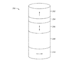
図2は、スタック内磁気バイアス層を有するMTJスタック200の一例を示す図である。図2に示すように、MTJスタック200は、固定層202、トンネルバリア層204、自由層206、パッシベーション層208、及びスタック内磁気バイアス層210を含む。MTJスタックの一実施例は、CoFeB磁気層202及び206、及び、トンネルバリア層204としてのMgOを含んでもよい。CoFeB−MgO MTJ(又は他の同様の種類のMTJ)は、電界がCeFeB/MgO境界面において電子の密度を変化させ、垂直異方性に影響を及ぼす電圧制御磁気異方性(VCMA)を呈する。例えば、界面における電子密度の低下は、垂直異方性を増加する。この磁気電気結合は、歪みを媒介としないため、耐久性に限界はなく、論理及びメモリ用途と互換性を持つ。
FIG. 2 is a diagram illustrating an example of an
外部磁界は、エネルギー障壁の向きを傾斜させる一方で、電圧制御異方性は、極性に応じて、エネルギー障壁を低下又は増加させるかのどちらかを行う。図3は、本開示のある特定の態様による、エネルギー障壁を調整するための磁界の印加を示している。エネルギー障壁を調整することは、電圧(パルス)が図4に示すように印加される場合、決定性スイッチングを可能にしてもよい。例えば、図4に示すように、MTJは、初期磁化Heffに整列される自由層磁性を有していてもよい。この実施例において、Heffは上を指し、界面の面外異方性によって支配される。電圧の印加は、結果として、MgO障壁を通る電界を生じ、界面異方性を低下させる。VCMA効果を介する自由層の磁気異方性のこの再構成は、電界を用いるスイッチングを可能にし、言い換えれば、VCMA効果による保磁力の低下が利用されて、スピン偏極電流に影響されることなく、本発明のVMTJの自由層の磁性を切り換える。図4に示すように、電圧パルスVpが印加されると、界面異方性磁界が低下し、ここで、Heffがスタック内層210からのバイアス磁界によって支配されるため、自由層に影響を及ぼす有効場Heffが面内で傾斜する。自由層の磁性は、それが最終的にHeffと整列するまで、Heffの周りを歳差運動する。減衰は、歳差運動が停止する前に、多くの振動が生じるという点で、システムにおいて十分低い。歳差運動は、Vpを遮断することによって中断でき、結果として、初期磁化方向とは反対の極性を有する最終的な磁化状態を生じることができる。
The external magnetic field tilts the direction of the energy barrier while the voltage controlled anisotropy either reduces or increases the energy barrier depending on the polarity. FIG. 3 illustrates the application of a magnetic field to adjust the energy barrier according to certain aspects of the present disclosure. Adjusting the energy barrier may allow deterministic switching when a voltage (pulse) is applied as shown in FIG. For example, as shown in FIG. 4, the MTJ may have free layer magnetism aligned with the initial magnetization H eff . In this example, H eff points up and is governed by the out-of-plane anisotropy of the interface. The application of a voltage results in an electric field through the MgO barrier and reduces the interface anisotropy. This reconfiguration of the magnetic anisotropy of the free layer via the VCMA effect enables switching using an electric field, in other words, a reduction in coercivity due to the VCMA effect is used and is not affected by the spin-polarized current. The magnetism of the free layer of the VMTJ of the present invention is switched. As shown in FIG. 4, when the voltage pulse V p is applied, the interface anisotropic magnetic field is reduced. Here, H eff is dominated by the bias magnetic field from the stack
かかる電界制御MTJは、相補型金属酸化膜半導体(CMOS)集積回路と互換性があってもよい。読み出しは、TMR効果を介して実行されてもよく、電気的な書き込みは、VCMAを用いて電界を介して実行されてもよい。書き込みは、例えば、1ns未満の共振(歳差運動)であってもよい。ビット同士は、スケーラビリティ及び密度のために垂直であってもよい。 Such an electric field control MTJ may be compatible with a complementary metal oxide semiconductor (CMOS) integrated circuit. Reading may be performed via the TMR effect and electrical writing may be performed via an electric field using VCMA. The writing may be, for example, resonance (precession) less than 1 ns. The bits may be vertical for scalability and density.
図5は、スタック内バイアス磁界を用いる垂直80nm×80nmMTJ装置のためのTMR読み出しとともにVCMA駆動の書き込みを示すグラフ500である。図5に示すように、100%スイッチングが達成できる(例えば、約700ps±250psの時間窓において)。この実施例において、スイッチングエネルギーは、1ns未満の書き込み時間で約10fJ/ビットであってもよい。この歳差運動のVCMAスイッチングは、決定性動作ではなくトグルである(すなわち、スイッチングは、VCMAパルスが印加される度に生じる)ため、読み出しは、ビットの極性及びトグルパルスが印加されるべきかどうかを決定するために、スイッチング前及び/又は後に行われてもよい。
FIG. 5 is a
従来、磁界は、図2に示すスタック内磁気バイアス層210のようなスタック内磁気バイアス層によって与えられる。
Conventionally, the magnetic field is provided by an in-stack magnetic bias layer, such as the in-stack
外部強磁性バイアス層を用いるVCMAスイッチング装置の実施例
本開示のある特定の態様による、外部(例えば、スタック内とは対照的な)磁石(例えば、バイアス層)を有する磁気トンネル接合(MTJ)装置を説明する。外部(例えば、永久)磁石の使用により、より簡単なスタックが可能となってもよい。
Example of a VCMA Switching Device Using an External Ferromagnetic Bias Layer A Magnetic Tunnel Junction (MTJ) Device with an External (eg, Contrast with a Stack) Magnet (eg, Bias Layer), According to Certain Aspects of the Present Disclosure Will be explained. The use of an external (eg permanent) magnet may allow easier stacking.
図6は、本開示のある特定の態様によるMRAM装置を製造するための操作600の一例を示す呼び出しフローである。例えば、操作600は、図7に示すMRAM装置700を製造するために用いられてもよい。
FIG. 6 is a call flow illustrating an example of an
602において、少なくとも1つのMTJスタック(例えば、MTJスタック704等)は、基板(例えば、基板702)上に形成されてもよく、ここで、MTJスタックは、固定磁化(例えば、固定層706)を有する第1の強磁性層(例えば、CoFeB層)と、非固定磁化(例えば、自由層710)を有する第2の強磁性層(例えば、CoFeB層)との間にトンネルバリア層(例えば、MgO層であってもよいトンネルバリア層708)を備えている。
At 602, at least one MTJ stack (eg,
604において、磁石(例えば、外部磁石712)は、第2の強磁性層に隣接して配設(例えば、形成)されてもよい。ある特定の態様によれば、磁石は、短絡を防止するよう(例えば、装置を切削加工した後)基板上に堆積されるパッシベーション層に配設されてもよい。ある特定の態様によれば、磁石は、基板(例えば、ウェーハ)上に形成される強磁性バイアス層(例えば、CoPt層等の硬質材料、又は、反強磁性体によって固定されるNiFe層等の軟質材料)であってもよい。図7に示すように、外部磁石712は、基板702と水平で平行に形成され、自由層710と整列されてもよい。
At 604, a magnet (eg, external magnet 712) may be disposed (eg, formed) adjacent to the second ferromagnetic layer. According to certain aspects, the magnet may be disposed in a passivation layer that is deposited on the substrate to prevent a short circuit (eg, after machining the device). According to certain aspects, the magnet may be a ferromagnetic bias layer (eg, a CoPt layer) formed on a substrate (eg, a wafer) or a NiFe layer pinned by an antiferromagnetic material. Soft material). As shown in FIG. 7, the
606において、自由層/バリア界面における垂直異方性が低下して(すなわち、VCMA効果)、自由層の磁化が、ここではバイアス磁石によって生じる磁界によって支配される有効場の周りで歳差運動する原因となるように、バイアス電圧がMTJスタックに印加される。パルス持続期間は、自由層の磁極性が反転するように、歳差運動を停止するよう最適化できる。ある特定の態様によれば、配設された磁石の厚さ、及び/又は、第2の強磁性層からの配設された磁石の距離は、所望の(例えば、最適な)磁界が磁石によってMTJスタックに作用するように、装置を製造する時に選択されてもよい。 At 606, the perpendicular anisotropy at the free layer / barrier interface is reduced (ie, the VCMA effect) and the free layer magnetization precesses around an effective field that is now governed by the magnetic field produced by the bias magnet. A bias voltage is applied to the MTJ stack to cause this. The pulse duration can be optimized to stop the precession so that the free layer magnetic polarity is reversed. According to certain aspects, the thickness of the disposed magnet and / or the distance of the disposed magnet from the second ferromagnetic layer may be such that the desired (e.g., optimal) magnetic field depends on the magnet. It may be selected when manufacturing the device to affect the MTJ stack.
ある特定の態様によれば、外部磁石は、イオンビーム蒸着(IBD)、電気メッキ、スパッタリング、又は、堆積させるための他の技法を用いて配設されてもよい。 According to certain aspects, the external magnet may be disposed using ion beam evaporation (IBD), electroplating, sputtering, or other techniques for deposition.
図7は、本開示のある特定の態様による、外部磁石712とともにMTJスタック704を有するMRAM装置700の一例を示す図である。ある特定の態様によれば、電界(例えば、VCMAパルス)がMTJスタックに印加される場合、自由層の磁化は、(外部磁石によって与えられる)永久バイアス磁界の周りを歳差運動してもよい。外部磁石のモーメント及び厚さの最適化は、所望の歳差磁界を与えるよう用いられてもよい。例えば、より強い磁界を用いることにより、より高速な歳差運動を与えてもよい。
FIG. 7 is a diagram illustrating an example of an
ある特定の態様によれば、外部磁界の使用により、向上した磁界制御、より大きな磁界を使用する能力、より容易にMTJスタックをエッチングする能力、及び、より簡単な磁性体に至ることができる。加えて、層がより薄く、エッチングを行うことがより簡単になるため、より狭い最終ピッチを用いることができる。更に、スタック内磁石は、自由層特性及び垂直異方性にとって好ましくないであろう、それらの方向を設定するために磁界をアニール処理する大きな面内磁界を必要としてもよい。加えて、高保磁力を有する永久磁性体(硬磁石)を外部磁石712に対して示してきたが、反強磁性バイアス層に結合される低保磁力(軟磁石)も使用できることは、言うまでもない。
According to certain aspects, the use of an external magnetic field can lead to improved magnetic field control, the ability to use a larger magnetic field, the ability to more easily etch the MTJ stack, and a simpler magnetic body. In addition, a narrower final pitch can be used because the layers are thinner and easier to etch. Furthermore, in-stack magnets may require a large in-plane magnetic field that anneals the magnetic field to set their direction, which would be undesirable for free layer properties and perpendicular anisotropy. In addition, although a permanent magnetic material (hard magnet) having a high coercivity has been shown for the
本明細書中に開示する方法は、説明した方法を達成するための1つ以上のステップ又は動作を含む。方法のステップ及び/又は動作は、特許請求の範囲の適用範囲から逸脱することなく、互いに交換されてもよい。言い換えれば、ステップ又は動作の特定の順序が明記されていなければ、特定のステップ及び/又は動作の順序及び/又は使用は、特許請求の範囲の適用範囲から逸脱することなく、変更されてもよい。 The methods disclosed herein include one or more steps or actions for achieving the described method. The method steps and / or actions may be interchanged with one another without departing from the scope of the claims. In other words, unless a specific order of steps or actions is specified, the order and / or use of specific steps and / or actions may be changed without departing from the scope of the claims. .
本明細書中で用いるように、項目のリストのうちの「少なくとも1つ」を指す表現は、単一の部材を含むこれらの項目の任意の組み合わせについて言及している。一例として、「a、b、又はcのうちの少なくとも1つ」は、a、b、c、a−b、a−c、b−c、及びa−b−c、並びに、同じ要素の集まりを持つ任意の組み合わせ(例えば、a−a、a−a−a、a−a−b、a−a−c、a−b−b、a−c−c、b−b、b−b−b、b−b−c、c−c、及びc−c−c、又は、a、b、及びcのその他の順序)をカバーすることを意図している。 As used herein, the expression “at least one” of a list of items refers to any combination of these items including a single member. By way of example, “at least one of a, b, or c” refers to a, b, c, ab, ac, bc, and abc, as well as a collection of the same elements. (For example, a-a, a-a-a, a-a-b, a-a-c, a-b-b, a-c-c, b-b, b-b- b, b-b-c, c-c, and c-c-c, or any other order of a, b, and c).
上で説明した方法の様々な操作は、対応する機能を実行できる任意の適切な手段によって行われてもよい。手段は、種々のハードウェア及び/又はソフトウェアコンポーネントを含んでもよい。 Various operations of the methods described above may be performed by any suitable means capable of performing the corresponding function. The means may include various hardware and / or software components.
特許請求の範囲は、上で示した厳密な構成及びコンポーネントに限定されないことは、言うまでもない。種々の改良、変更、変形が、特許請求の範囲の適用範囲から逸脱することなく、上で説明した方法及び装置の配置、操作、及び詳細において行われてもよい。 It will be appreciated that the claims are not limited to the precise configuration and components illustrated above. Various modifications, changes and variations may be made in the arrangement, operation and details of the methods and apparatus described above without departing from the scope of the claims.
100、200、704 MTJスタック
102 永久磁石
104、204、708 トンネルバリア層
106 プレート
202、706 固定層
206、710 自由層
208 パッシベーション層
210 スタック内磁気バイアス層
600 操作
700 MRAM装置
702 基板
712 外部磁石
100, 200, 704
Claims (20)
基板と、
前記基板上に配設される少なくとも1つの磁気トンネル接合(MTJ)スタックであって、固定磁化を有する第1の強磁性層と、非固定磁化を有する第2の強磁性層との間にトンネルバリア層を備えるMTJスタックと、
前記第2の強磁性層に隣接して配設される磁石と、を備える、
MRAM装置。 A magnetoresistive random access memory (MRAM) device comprising:
A substrate,
At least one magnetic tunnel junction (MTJ) stack disposed on the substrate, wherein the tunnel is between a first ferromagnetic layer having a fixed magnetization and a second ferromagnetic layer having a non-fixed magnetization. An MTJ stack comprising a barrier layer;
A magnet disposed adjacent to the second ferromagnetic layer,
MRAM device.
少なくとも1つの磁気トンネル接合(MTJ)スタックを基板上に形成することであって、前記MTJスタックが、固定磁化を有する第1の強磁性層と、非固定磁化を有する第2の強磁性層との間にトンネルバリア層を備えることと、
磁石を前記第2の強磁性層に隣接して配設することと、を含む、
方法。 A method for manufacturing a magnetoresistive random access memory (MRAM) device comprising:
Forming at least one magnetic tunnel junction (MTJ) stack on a substrate, the MTJ stack comprising: a first ferromagnetic layer having a fixed magnetization; and a second ferromagnetic layer having a non-fixed magnetization; Providing a tunnel barrier layer between,
Disposing a magnet adjacent to the second ferromagnetic layer;
Method.
基板と、
前記基板上に配設される少なくとも1つの磁気トンネル接合(MTJ)スタックであって、固定磁化を有する第1の強磁性層と、非固定磁化を有する第2の強磁性層との間にトンネルバリア層を備えるMTJスタックと、
前記基板上に形成されるパッシベーション層であって、MTJ間の空間を埋めるパッシベーション層と、
前記第2の強磁性層に隣接して前記パッシベーション層内に配設される磁石であって、前記磁石は、前記基板と水平で平行に配設され、前記第2の強磁性層と整列される強磁性バイアス層を備え、電界が前記MTJスタックに印加された場合に、前記MTJスタックの磁極性が反転されるように、バイアス電圧が前記MTJスタックに印加された場合に、前記第2の強磁性層の磁化が、前記磁石からのバイアス磁界の周りを歳差運動する磁石と、を備える、
MRAM装置。 A magnetoresistive random access memory (MRAM) device comprising:
A substrate,
At least one magnetic tunnel junction (MTJ) stack disposed on the substrate, wherein the tunnel is between a first ferromagnetic layer having a fixed magnetization and a second ferromagnetic layer having a non-fixed magnetization. An MTJ stack comprising a barrier layer;
A passivation layer formed on the substrate, the passivation layer filling a space between the MTJs;
A magnet disposed in the passivation layer adjacent to the second ferromagnetic layer, the magnet disposed horizontally and parallel to the substrate and aligned with the second ferromagnetic layer; And when the bias voltage is applied to the MTJ stack, the second polarity is reversed so that the magnetic polarity of the MTJ stack is reversed when an electric field is applied to the MTJ stack. The magnetization of the ferromagnetic layer comprises a magnet that precesses around a bias magnetic field from the magnet;
MRAM device.
Applications Claiming Priority (2)
| Application Number | Priority Date | Filing Date | Title |
|---|---|---|---|
| US14/728,788 | 2015-06-02 | ||
| US14/728,788 US9620562B2 (en) | 2015-06-02 | 2015-06-02 | Voltage-controlled magnetic anisotropy switching device using an external ferromagnetic biasing film |
Publications (1)
| Publication Number | Publication Date |
|---|---|
| JP2016225633A true JP2016225633A (en) | 2016-12-28 |
Family
ID=56410819
Family Applications (1)
| Application Number | Title | Priority Date | Filing Date |
|---|---|---|---|
| JP2016111167A Pending JP2016225633A (en) | 2015-06-02 | 2016-06-02 | Voltage-controlled magnetic anisotropy switching device using external ferromagnetic biasing film |
Country Status (8)
| Country | Link |
|---|---|
| US (1) | US9620562B2 (en) |
| JP (1) | JP2016225633A (en) |
| KR (1) | KR101869149B1 (en) |
| CN (1) | CN106374035B (en) |
| DE (1) | DE102016006651A1 (en) |
| FR (1) | FR3037185B1 (en) |
| GB (1) | GB2539102B (en) |
| TW (1) | TWI602331B (en) |
Cited By (3)
| Publication number | Priority date | Publication date | Assignee | Title |
|---|---|---|---|---|
| WO2018198713A1 (en) * | 2017-04-28 | 2018-11-01 | 国立研究開発法人産業技術総合研究所 | Magnetic element |
| JP2020021782A (en) * | 2018-07-30 | 2020-02-06 | 株式会社東芝 | Magnetic storage device |
| WO2023090132A1 (en) * | 2021-11-17 | 2023-05-25 | ソニーセミコンダクタソリューションズ株式会社 | Magnetoresistive effect memory, memory array, and memory system |
Families Citing this family (21)
| Publication number | Priority date | Publication date | Assignee | Title |
|---|---|---|---|---|
| US10103317B2 (en) | 2015-01-05 | 2018-10-16 | Inston, Inc. | Systems and methods for implementing efficient magnetoelectric junctions |
| US10217798B2 (en) | 2015-01-13 | 2019-02-26 | Inston, Inc. | Systems and methods for implementing select devices constructed from 2D materials |
| US9978931B2 (en) | 2015-02-13 | 2018-05-22 | Inston Inc. | Systems and methods for implementing robust magnetoelectric junctions |
| US20170033281A1 (en) * | 2015-07-29 | 2017-02-02 | Inston Inc. | Systems and Methods for Implementing Magnetoelectric Junctions Including Integrated Magnetization Components |
| US10102893B2 (en) | 2016-06-28 | 2018-10-16 | Inston Inc. | Systems for implementing word line pulse techniques in magnetoelectric junctions |
| US10861527B2 (en) | 2017-06-27 | 2020-12-08 | Inston, Inc. | Systems and methods for optimizing magnetic torque and pulse shaping for reducing write error rate in magnetoelectric random access memory |
| US10460786B2 (en) | 2017-06-27 | 2019-10-29 | Inston, Inc. | Systems and methods for reducing write error rate in magnetoelectric random access memory through pulse sharpening and reverse pulse schemes |
| JP2019057601A (en) | 2017-09-20 | 2019-04-11 | 東芝メモリ株式会社 | Magnetic memory device |
| US10593866B2 (en) * | 2018-06-27 | 2020-03-17 | Globalfoundries Singapore Pte. Ltd. | Magnetic field assisted MRAM structures, integrated circuits, and methods for fabricating the same |
| US10636962B2 (en) | 2018-08-21 | 2020-04-28 | Qualcomm Incorporated | Spin-orbit torque (SOT) magnetic tunnel junction (MTJ) (SOT-MTJ) devices employing perpendicular and in-plane free layer magnetic anisotropy to facilitate perpendicular magnetic orientation switching, suitable for use in memory systems for storing data |
| US11195991B2 (en) * | 2018-09-27 | 2021-12-07 | Taiwan Semiconductor Manufacturing Company, Ltd. | Magnetic random access memory assisted devices and methods of making |
| EP3671874B1 (en) | 2018-12-21 | 2022-06-22 | IMEC vzw | Zero-field switching for sot technology |
| CN110061127B (en) * | 2019-05-20 | 2023-08-08 | 中国科学院微电子研究所 | Magnetic tunnel junction forming method and magneto-resistive random access memory |
| CN112310274A (en) * | 2019-07-31 | 2021-02-02 | 中电海康集团有限公司 | Spin-orbit torque magnetic memory unit and preparation method thereof |
| US11069390B2 (en) * | 2019-09-06 | 2021-07-20 | Wisconsin Alumni Research Foundation | Spin-orbit torque magnetoresistive random access memory with magnetic field-free current-induced perpendicular magnetization reversal |
| CN111490156A (en) * | 2020-04-21 | 2020-08-04 | 浙江驰拓科技有限公司 | Spin orbit torque magnetic memory device and preparation method thereof |
| US11264562B1 (en) | 2020-08-27 | 2022-03-01 | Western Digital Technologies, Inc. | Multiferroic-assisted voltage controlled magnetic anisotropy memory device and methods of manufacturing the same |
| US11276446B1 (en) | 2020-08-27 | 2022-03-15 | Western Digital Technologies, Inc. | Multiferroic-assisted voltage controlled magnetic anisotropy memory device and methods of manufacturing the same |
| WO2022046237A1 (en) * | 2020-08-27 | 2022-03-03 | Western Digital Technologies, Inc. | Multiferroic-assisted voltage controlled magnetic anisotropy memory device and methods of manufacturing the same |
| US20220108158A1 (en) * | 2020-10-02 | 2022-04-07 | Sandisk Technologies Llc | Ultralow power inference engine with external magnetic field programming assistance |
| US11729996B2 (en) | 2021-07-30 | 2023-08-15 | International Business Machines Corporation | High retention eMRAM using VCMA-assisted writing |
Citations (6)
| Publication number | Priority date | Publication date | Assignee | Title |
|---|---|---|---|---|
| JP2006179524A (en) * | 2004-12-20 | 2006-07-06 | Toshiba Corp | Magnetic recoding element, magnetic recording device and information recording method |
| US7230845B1 (en) * | 2005-07-29 | 2007-06-12 | Grandis, Inc. | Magnetic devices having a hard bias field and magnetic memory devices using the magnetic devices |
| JP2008135432A (en) * | 2006-11-27 | 2008-06-12 | Tdk Corp | Tunnel magnetoresistive effect element and manufacturing method thereof |
| JP2008171882A (en) * | 2007-01-09 | 2008-07-24 | Sony Corp | Storage element and memory |
| JP2008198900A (en) * | 2007-02-15 | 2008-08-28 | Toshiba Corp | Magnetic memory element and magnetic storage device |
| JP2009245500A (en) * | 2008-03-31 | 2009-10-22 | Tdk Corp | Magnetic storage device |
Family Cites Families (18)
| Publication number | Priority date | Publication date | Assignee | Title |
|---|---|---|---|---|
| US5729410A (en) | 1996-11-27 | 1998-03-17 | International Business Machines Corporation | Magnetic tunnel junction device with longitudinal biasing |
| US5936293A (en) * | 1998-01-23 | 1999-08-10 | International Business Machines Corporation | Hard/soft magnetic tunnel junction device with stable hard ferromagnetic layer |
| US6114719A (en) | 1998-05-29 | 2000-09-05 | International Business Machines Corporation | Magnetic tunnel junction memory cell with in-stack biasing of the free ferromagnetic layer and memory array using the cell |
| US8755222B2 (en) * | 2003-08-19 | 2014-06-17 | New York University | Bipolar spin-transfer switching |
| US7285836B2 (en) * | 2005-03-09 | 2007-10-23 | Maglabs, Inc. | Magnetic random access memory with stacked memory cells having oppositely-directed hard-axis biasing |
| US7777261B2 (en) | 2005-09-20 | 2010-08-17 | Grandis Inc. | Magnetic device having stabilized free ferromagnetic layer |
| US8058696B2 (en) * | 2006-02-25 | 2011-11-15 | Avalanche Technology, Inc. | High capacity low cost multi-state magnetic memory |
| FR2914482B1 (en) * | 2007-03-29 | 2009-05-29 | Commissariat Energie Atomique | MAGNETIC MEMORY WITH MAGNETIC TUNNEL JUNCTION |
| EP2015307B8 (en) * | 2007-07-13 | 2013-05-15 | Hitachi Ltd. | Magnetoresistive device |
| US8039913B2 (en) * | 2008-10-09 | 2011-10-18 | Seagate Technology Llc | Magnetic stack with laminated layer |
| US9728240B2 (en) | 2009-04-08 | 2017-08-08 | Avalanche Technology, Inc. | Pulse programming techniques for voltage-controlled magnetoresistive tunnel junction (MTJ) |
| US9196332B2 (en) * | 2011-02-16 | 2015-11-24 | Avalanche Technology, Inc. | Perpendicular magnetic tunnel junction (pMTJ) with in-plane magneto-static switching-enhancing layer |
| CN103563000B (en) * | 2011-05-19 | 2016-12-07 | 加利福尼亚大学董事会 | Voltage-controlled magnetic anisotropy (VCMA) switch and electromagnetic storage (MERAM) |
| US9293694B2 (en) * | 2011-11-03 | 2016-03-22 | Ge Yi | Magnetoresistive random access memory cell with independently operating read and write components |
| WO2014022304A1 (en) | 2012-07-30 | 2014-02-06 | The Regents Of The University Of California | Multiple-bits-per-cell voltage-controlled magnetic memory |
| KR101649978B1 (en) | 2012-08-06 | 2016-08-22 | 코넬 유니버시티 | Electrically gated three-terminal circuits and devices based on spin hall torque effects in magnetic nanostructures |
| US8988923B2 (en) | 2012-09-11 | 2015-03-24 | The Regents Of The University Of California | Nonvolatile magneto-electric random access memory circuit with burst writing and back-to-back reads |
| US9036407B2 (en) | 2012-12-07 | 2015-05-19 | The Regents Of The University Of California | Voltage-controlled magnetic memory element with canted magnetization |
-
2015
- 2015-06-02 US US14/728,788 patent/US9620562B2/en not_active Expired - Fee Related
-
2016
- 2016-06-01 FR FR1654982A patent/FR3037185B1/en not_active Expired - Fee Related
- 2016-06-01 GB GB1609565.5A patent/GB2539102B/en not_active Expired - Fee Related
- 2016-06-02 JP JP2016111167A patent/JP2016225633A/en active Pending
- 2016-06-02 TW TW105117430A patent/TWI602331B/en not_active IP Right Cessation
- 2016-06-02 CN CN201610826624.8A patent/CN106374035B/en active Active
- 2016-06-02 KR KR1020160068948A patent/KR101869149B1/en active IP Right Grant
- 2016-06-02 DE DE102016006651.2A patent/DE102016006651A1/en active Pending
Patent Citations (6)
| Publication number | Priority date | Publication date | Assignee | Title |
|---|---|---|---|---|
| JP2006179524A (en) * | 2004-12-20 | 2006-07-06 | Toshiba Corp | Magnetic recoding element, magnetic recording device and information recording method |
| US7230845B1 (en) * | 2005-07-29 | 2007-06-12 | Grandis, Inc. | Magnetic devices having a hard bias field and magnetic memory devices using the magnetic devices |
| JP2008135432A (en) * | 2006-11-27 | 2008-06-12 | Tdk Corp | Tunnel magnetoresistive effect element and manufacturing method thereof |
| JP2008171882A (en) * | 2007-01-09 | 2008-07-24 | Sony Corp | Storage element and memory |
| JP2008198900A (en) * | 2007-02-15 | 2008-08-28 | Toshiba Corp | Magnetic memory element and magnetic storage device |
| JP2009245500A (en) * | 2008-03-31 | 2009-10-22 | Tdk Corp | Magnetic storage device |
Cited By (6)
| Publication number | Priority date | Publication date | Assignee | Title |
|---|---|---|---|---|
| WO2018198713A1 (en) * | 2017-04-28 | 2018-11-01 | 国立研究開発法人産業技術総合研究所 | Magnetic element |
| JPWO2018198713A1 (en) * | 2017-04-28 | 2019-11-07 | 国立研究開発法人産業技術総合研究所 | Magnetic element |
| US10998490B2 (en) | 2017-04-28 | 2021-05-04 | National Institute Of Advanced Industrial Science And Technology | Magnetic element |
| JP2020021782A (en) * | 2018-07-30 | 2020-02-06 | 株式会社東芝 | Magnetic storage device |
| JP7005452B2 (en) | 2018-07-30 | 2022-01-21 | 株式会社東芝 | Magnetic storage device |
| WO2023090132A1 (en) * | 2021-11-17 | 2023-05-25 | ソニーセミコンダクタソリューションズ株式会社 | Magnetoresistive effect memory, memory array, and memory system |
Also Published As
| Publication number | Publication date |
|---|---|
| GB2539102A (en) | 2016-12-07 |
| KR101869149B1 (en) | 2018-06-19 |
| KR20160142255A (en) | 2016-12-12 |
| US20160358973A1 (en) | 2016-12-08 |
| DE102016006651A1 (en) | 2016-12-08 |
| TW201705568A (en) | 2017-02-01 |
| US9620562B2 (en) | 2017-04-11 |
| GB201609565D0 (en) | 2016-07-13 |
| TWI602331B (en) | 2017-10-11 |
| FR3037185B1 (en) | 2019-10-25 |
| GB2539102B (en) | 2019-09-11 |
| FR3037185A1 (en) | 2016-12-09 |
| CN106374035A (en) | 2017-02-01 |
| CN106374035B (en) | 2019-11-26 |
Similar Documents
| Publication | Publication Date | Title |
|---|---|---|
| TWI602331B (en) | Voltage-controlled magnetic anisotropy switching device using an external ferromagnetic biasing film | |
| KR102353406B1 (en) | Magnetic devices including magnetic junctions having tilted easy axes and enhanced damping programmable using spin orbit torque | |
| RU2595588C2 (en) | Magnetic recording element | |
| KR102099192B1 (en) | Cross point array mram having spin hall mtj devices | |
| US8514615B2 (en) | Structures and methods for a field-reset spin-torque MRAM | |
| US8228715B2 (en) | Structures and methods for a field-reset spin-torque MRAM | |
| US7965543B2 (en) | Method for reducing current density in a magnetoelectronic device | |
| JP2017112359A (en) | Top pinned sot-mram architecture with in-stack selector | |
| US20180268886A1 (en) | Magnetic memory | |
| EP1653475A1 (en) | Multi-bit magnetic random access memory device and method for writing the same | |
| JP2014064033A (en) | High speed low power magnetic device based on current-induced spin-momentum transfer | |
| US10461242B2 (en) | Antiferromagnetic exchange coupling enhancement in perpendicular magnetic tunnel junction stacks for magnetic random access memory applications | |
| US10832847B2 (en) | Low stray field magnetic memory | |
| EP2656346B1 (en) | Memory array having local source lines | |
| US20220149269A1 (en) | Spintronics element and magnetic memory device | |
| US10783943B2 (en) | MRAM having novel self-referenced read method | |
| US11521776B2 (en) | Spin-orbit-torque magnetization rotational element, spin-orbit-torque magnetoresistance effect element, and spin-orbit-torque magnetization rotational element manufacturing method | |
| US10902987B2 (en) | Spin-orbit torque type magnetization rotation element, spin-orbit torque magnetoresistance effect element, and method of manufacturing spin-orbit torque type magnetization rotation element | |
| US20200020376A1 (en) | Magnetic memory and magnetic memory recording method | |
| US20130033927A1 (en) | Magentic resistance memory apparatus having multi levels and method of driving the same | |
| US10269400B2 (en) | Tilted synthetic antiferromagnet polarizer/reference layer for STT-MRAM bits | |
| JP2013197518A (en) | Magnetic tunnel junction element and magnetic memory | |
| CN110366756A (en) | Magnetic memory, semiconductor device, electronic equipment and the method for reading magnetic memory | |
| KR102433984B1 (en) | Method and system for providing magnetic junctions including self-initializing reference layers |
Legal Events
| Date | Code | Title | Description |
|---|---|---|---|
| A977 | Report on retrieval |
Free format text: JAPANESE INTERMEDIATE CODE: A971007 Effective date: 20170406 |
|
| A131 | Notification of reasons for refusal |
Free format text: JAPANESE INTERMEDIATE CODE: A131 Effective date: 20170418 |
|
| A521 | Request for written amendment filed |
Free format text: JAPANESE INTERMEDIATE CODE: A523 Effective date: 20170718 |
|
| RD02 | Notification of acceptance of power of attorney |
Free format text: JAPANESE INTERMEDIATE CODE: A7422 Effective date: 20170810 |
|
| RD04 | Notification of resignation of power of attorney |
Free format text: JAPANESE INTERMEDIATE CODE: A7424 Effective date: 20170825 |
|
| A131 | Notification of reasons for refusal |
Free format text: JAPANESE INTERMEDIATE CODE: A131 Effective date: 20171128 |
|
| A521 | Request for written amendment filed |
Free format text: JAPANESE INTERMEDIATE CODE: A523 Effective date: 20180219 |
|
| A02 | Decision of refusal |
Free format text: JAPANESE INTERMEDIATE CODE: A02 Effective date: 20180703 |