JP2016122676A - Exposure device and exposure method - Google Patents

Exposure device and exposure method Download PDF

Info

Publication number
JP2016122676A
JP2016122676A JP2014260001A JP2014260001A JP2016122676A JP 2016122676 A JP2016122676 A JP 2016122676A JP 2014260001 A JP2014260001 A JP 2014260001A JP 2014260001 A JP2014260001 A JP 2014260001A JP 2016122676 A JP2016122676 A JP 2016122676A
Authority
JP
Japan
Prior art keywords
charged particle
sample
irradiation
line pattern
pattern
Prior art date
Legal status (The legal status is an assumption and is not a legal conclusion. Google has not performed a legal analysis and makes no representation as to the accuracy of the status listed.)
Pending
Application number
JP2014260001A
Other languages
Japanese (ja)
Inventor
山田 章夫
Akio Yamada
章夫 山田
慎二 菅谷
Shinji Sugaya
慎二 菅谷
正樹 黒川
Masaki Kurokawa
正樹 黒川
瀬山 雅裕
Masahiro Seyama
雅裕 瀬山
Current Assignee (The listed assignees may be inaccurate. Google has not performed a legal analysis and makes no representation or warranty as to the accuracy of the list.)
Advantest Corp
Original Assignee
Advantest Corp
Priority date (The priority date is an assumption and is not a legal conclusion. Google has not performed a legal analysis and makes no representation as to the accuracy of the date listed.)
Filing date
Publication date
Application filed by Advantest Corp filed Critical Advantest Corp
Priority to JP2014260001A priority Critical patent/JP2016122676A/en
Priority to TW106123688A priority patent/TWI669743B/en
Priority to TW104133390A priority patent/TWI600047B/en
Priority to US14/883,634 priority patent/US9734988B2/en
Priority to KR1020150144061A priority patent/KR101772545B1/en
Priority to EP15189949.9A priority patent/EP3038130A3/en
Priority to CN201510673307.2A priority patent/CN105739246B/en
Publication of JP2016122676A publication Critical patent/JP2016122676A/en
Priority to US15/671,112 priority patent/US10256074B2/en
Priority to KR1020170106028A priority patent/KR102207024B1/en
Pending legal-status Critical Current

Links

Images

Classifications

    • GPHYSICS
    • G03PHOTOGRAPHY; CINEMATOGRAPHY; ANALOGOUS TECHNIQUES USING WAVES OTHER THAN OPTICAL WAVES; ELECTROGRAPHY; HOLOGRAPHY
    • G03FPHOTOMECHANICAL PRODUCTION OF TEXTURED OR PATTERNED SURFACES, e.g. FOR PRINTING, FOR PROCESSING OF SEMICONDUCTOR DEVICES; MATERIALS THEREFOR; ORIGINALS THEREFOR; APPARATUS SPECIALLY ADAPTED THEREFOR
    • G03F7/00Photomechanical, e.g. photolithographic, production of textured or patterned surfaces, e.g. printing surfaces; Materials therefor, e.g. comprising photoresists; Apparatus specially adapted therefor
    • G03F7/20Exposure; Apparatus therefor
    • G03F7/2051Exposure without an original mask, e.g. using a programmed deflection of a point source, by scanning, by drawing with a light beam, using an addressed light or corpuscular source
    • G03F7/2059Exposure without an original mask, e.g. using a programmed deflection of a point source, by scanning, by drawing with a light beam, using an addressed light or corpuscular source using a scanning corpuscular radiation beam, e.g. an electron beam
    • HELECTRICITY
    • H01ELECTRIC ELEMENTS
    • H01JELECTRIC DISCHARGE TUBES OR DISCHARGE LAMPS
    • H01J37/00Discharge tubes with provision for introducing objects or material to be exposed to the discharge, e.g. for the purpose of examination or processing thereof
    • H01J37/30Electron-beam or ion-beam tubes for localised treatment of objects
    • H01J37/317Electron-beam or ion-beam tubes for localised treatment of objects for changing properties of the objects or for applying thin layers thereon, e.g. for ion implantation
    • H01J37/3174Particle-beam lithography, e.g. electron beam lithography
    • GPHYSICS
    • G03PHOTOGRAPHY; CINEMATOGRAPHY; ANALOGOUS TECHNIQUES USING WAVES OTHER THAN OPTICAL WAVES; ELECTROGRAPHY; HOLOGRAPHY
    • G03FPHOTOMECHANICAL PRODUCTION OF TEXTURED OR PATTERNED SURFACES, e.g. FOR PRINTING, FOR PROCESSING OF SEMICONDUCTOR DEVICES; MATERIALS THEREFOR; ORIGINALS THEREFOR; APPARATUS SPECIALLY ADAPTED THEREFOR
    • G03F1/00Originals for photomechanical production of textured or patterned surfaces, e.g., masks, photo-masks, reticles; Mask blanks or pellicles therefor; Containers specially adapted therefor; Preparation thereof
    • G03F1/20Masks or mask blanks for imaging by charged particle beam [CPB] radiation, e.g. by electron beam; Preparation thereof
    • GPHYSICS
    • G03PHOTOGRAPHY; CINEMATOGRAPHY; ANALOGOUS TECHNIQUES USING WAVES OTHER THAN OPTICAL WAVES; ELECTROGRAPHY; HOLOGRAPHY
    • G03FPHOTOMECHANICAL PRODUCTION OF TEXTURED OR PATTERNED SURFACES, e.g. FOR PRINTING, FOR PROCESSING OF SEMICONDUCTOR DEVICES; MATERIALS THEREFOR; ORIGINALS THEREFOR; APPARATUS SPECIALLY ADAPTED THEREFOR
    • G03F1/00Originals for photomechanical production of textured or patterned surfaces, e.g., masks, photo-masks, reticles; Mask blanks or pellicles therefor; Containers specially adapted therefor; Preparation thereof
    • G03F1/22Masks or mask blanks for imaging by radiation of 100nm or shorter wavelength, e.g. X-ray masks, extreme ultraviolet [EUV] masks; Preparation thereof
    • HELECTRICITY
    • H01ELECTRIC ELEMENTS
    • H01JELECTRIC DISCHARGE TUBES OR DISCHARGE LAMPS
    • H01J37/00Discharge tubes with provision for introducing objects or material to be exposed to the discharge, e.g. for the purpose of examination or processing thereof
    • H01J37/02Details
    • H01J37/04Arrangements of electrodes and associated parts for generating or controlling the discharge, e.g. electron-optical arrangement, ion-optical arrangement
    • H01J37/045Beam blanking or chopping, i.e. arrangements for momentarily interrupting exposure to the discharge
    • HELECTRICITY
    • H01ELECTRIC ELEMENTS
    • H01JELECTRIC DISCHARGE TUBES OR DISCHARGE LAMPS
    • H01J37/00Discharge tubes with provision for introducing objects or material to be exposed to the discharge, e.g. for the purpose of examination or processing thereof
    • H01J37/30Electron-beam or ion-beam tubes for localised treatment of objects
    • H01J37/317Electron-beam or ion-beam tubes for localised treatment of objects for changing properties of the objects or for applying thin layers thereon, e.g. for ion implantation
    • H01J37/3174Particle-beam lithography, e.g. electron beam lithography
    • H01J37/3177Multi-beam, e.g. fly's eye, comb probe
    • HELECTRICITY
    • H01ELECTRIC ELEMENTS
    • H01JELECTRIC DISCHARGE TUBES OR DISCHARGE LAMPS
    • H01J2237/00Discharge tubes exposing object to beam, e.g. for analysis treatment, etching, imaging
    • H01J2237/30Electron or ion beam tubes for processing objects
    • H01J2237/317Processing objects on a microscale
    • H01J2237/3175Lithography
    • H01J2237/31761Patterning strategy
    • H01J2237/31766Continuous moving of wafer
    • HELECTRICITY
    • H01ELECTRIC ELEMENTS
    • H01JELECTRIC DISCHARGE TUBES OR DISCHARGE LAMPS
    • H01J2237/00Discharge tubes exposing object to beam, e.g. for analysis treatment, etching, imaging
    • H01J2237/30Electron or ion beam tubes for processing objects
    • H01J2237/317Processing objects on a microscale
    • H01J2237/3175Lithography
    • H01J2237/31774Multi-beam

Abstract

PROBLEM TO BE SOLVED: To provide exposure device and method that form a complicated fine pattern by combining an optical exposure technique and a charged particle beam exposure technique.SOLUTION: An exposure device that applies a charged particle beam to a position corresponding to a line pattern on a sample, and an exposure method are provided. The exposure device has a beam generator for generating plural charged particle beams for different irradiation positions in the width direction of the line pattern, a sweep controller for sweeping the irradiation positions of the plural charged particle beams along the longitudinal direction of the line pattern, a selector for selecting at least one charged particle beam to be applied to the sample from the plural charged particle beams at a specified irradiation position in the longitudinal direction on the line pattern, and an irradiation controller for controlling irradiation of the sample with the at least one selected charged particle beam.SELECTED DRAWING: Figure 1

Description

本発明は、露光装置および露光方法に関する。   The present invention relates to an exposure apparatus and an exposure method.

従来、線幅が数十nm程度の光露光技術で形成した単純なラインパターンに、電子ビーム等の荷電粒子ビームを用いた露光技術を用いて加工することで、微細な配線パターンを形成するコンプリメンタリ・リソグラフィが知られている(例えば、特許文献1および2参照)。また、荷電粒子ビームを複数用いたマルチビーム露光技術も知られている(例えば、特許文献3および4参照)。
特許文献1 特開2013−16744号公報
特許文献2 特開2013−157547号公報
特許文献3 米国特許第7276714号明細書
特許文献4 特開2013−93566号公報
Complementary to form a fine wiring pattern by processing an exposure technique using a charged particle beam such as an electron beam into a simple line pattern that has been conventionally formed by a light exposure technique with a line width of about several tens of nanometers. Lithography is known (see, for example, Patent Documents 1 and 2). A multi-beam exposure technique using a plurality of charged particle beams is also known (see, for example, Patent Documents 3 and 4).
Patent Literature 1 JP 2013-16744 A Patent Literature 2 JP 2013-157547 A Patent Literature 3 US Pat. No. 7,276,714 Patent Literature 4 JP 2013-93566 A

しかしながら、このような手法において、複数の荷電粒子ビームをパターンに照射するマルチビーム露光技術を用いると、異なる線幅および異なるピッチで形成されたラインパターンを当該マルチビームで加工することは困難であった。その一方で、作製すべき半導体装置のパターンは、同一線幅かつ同一ピッチの単純なラインパターンを加工するだけでは対応できない場合もあり、異なる線幅および異なるピッチで形成されたラインパターンを加工できる技術が望まれていた。   However, in such a method, when a multi-beam exposure technique in which a pattern is irradiated with a plurality of charged particle beams is used, it is difficult to process line patterns formed with different line widths and different pitches with the multi-beam. It was. On the other hand, the pattern of the semiconductor device to be manufactured may not be able to be dealt with by simply processing a simple line pattern having the same line width and the same pitch, and a line pattern formed with a different line width and a different pitch can be processed. Technology was desired.

本発明の第1の態様においては、試料上のラインパターンに応じた位置に荷電粒子ビームを照射する露光装置であって、ラインパターンの幅方向に照射位置が異なる複数の荷電粒子ビームを発生するビーム発生部と、複数の荷電粒子ビームの照射位置を、ラインパターンの長手方向に沿って走査させる走査制御部と、ラインパターン上の長手方向の指定された照射位置において、複数の荷電粒子ビームのうち試料に照射すべき少なくとも1つの荷電粒子ビームを選択する選択部と、選択された少なくとも1つの荷電粒子ビームを試料へと照射する制御をする照射制御部と、を備える露光装置および露光方法を提供する。   In the first aspect of the present invention, an exposure apparatus that irradiates a charged particle beam at a position corresponding to a line pattern on a sample, and generates a plurality of charged particle beams having different irradiation positions in the width direction of the line pattern. A beam generation unit, a scanning control unit that scans irradiation positions of a plurality of charged particle beams along the longitudinal direction of the line pattern, and a plurality of charged particle beams at a specified irradiation position in the longitudinal direction on the line pattern. An exposure apparatus and an exposure method comprising: a selection unit that selects at least one charged particle beam to be irradiated onto a sample; and an irradiation control unit that controls to irradiate the sample with at least one selected charged particle beam. provide.

なお、上記の発明の概要は、本発明の必要な特徴の全てを列挙したものではない。また、これらの特徴群のサブコンビネーションもまた、発明となりうる。   It should be noted that the above summary of the invention does not enumerate all the necessary features of the present invention. In addition, a sub-combination of these feature groups can also be an invention.

本実施形態に係る露光装置100の構成例を示す。2 shows a configuration example of an exposure apparatus 100 according to the present embodiment. 本実施形態に係る露光装置100がアレイビームを走査して、試料10の表面の一部に形成する照射可能領域200の一例を示す。An example of an irradiable region 200 formed on a part of the surface of the sample 10 by the exposure apparatus 100 according to the present embodiment scanning an array beam is shown. 本実施形態に係る露光装置100の動作フローを示す。2 shows an operation flow of the exposure apparatus 100 according to the present embodiment. 試料10に形成すべきカットパターンの情報の一例を示す。An example of cut pattern information to be formed on the sample 10 is shown. 本実施形態に係る走査制御部190がアレイビームの照射位置をフレームの開始点に移動した場合の一例を示す。An example in which the scanning control unit 190 according to the present embodiment moves the irradiation position of the array beam to the start point of the frame is shown. 本実施形態に係る選択部160の一例を示す。An example of the selection part 160 which concerns on this embodiment is shown. 本実施形態に係る露光制御部140が、ブランキング電極64に供給する制御信号のタイミングチャートの一例を示す。An example of a timing chart of control signals supplied to the blanking electrode 64 by the exposure control unit 140 according to the present embodiment is shown. 試料10の表面に形成されたラインパターン802の一例を示す。An example of the line pattern 802 formed on the surface of the sample 10 is shown. 試料10の表面に形成された配線パターン900の一例を示す。An example of the wiring pattern 900 formed on the surface of the sample 10 is shown. 異なるライン幅および異なるライン間隔のラインパターンが形成された試料10の一例を示す。An example of the sample 10 in which line patterns having different line widths and different line intervals are formed is shown. 本実施形態に係る電子ビームの照射領域502を、グリッド800に対応させて配置した例を示す。An example in which an electron beam irradiation area 502 according to the present embodiment is arranged in correspondence with a grid 800 is shown. 本実施形態に係る照射制御部170が生成したカットパターンの露光量を調節する制御信号の一例を示す。An example of the control signal which adjusts the exposure amount of the cut pattern which the irradiation control part 170 which concerns on this embodiment produced | generated is shown. 図12に示すタイミングチャートに示す露光量制御を実行する選択部160の構成例を示す。13 shows a configuration example of a selection unit 160 that performs exposure amount control shown in the timing chart shown in FIG. 12. 本実施形態に係るブランキング部60の一例を示す。An example of the blanking part 60 which concerns on this embodiment is shown. 本実施形態に係る露光装置100の変形例を示す。The modification of the exposure apparatus 100 which concerns on this embodiment is shown.

以下、発明の実施の形態を通じて本発明を説明するが、以下の実施形態は特許請求の範囲にかかる発明を限定するものではない。また、実施形態の中で説明されている特徴の組み合わせの全てが発明の解決手段に必須であるとは限らない。   Hereinafter, the present invention will be described through embodiments of the invention, but the following embodiments do not limit the invention according to the claims. In addition, not all the combinations of features described in the embodiments are essential for the solving means of the invention.

図1は、本実施形態に係る露光装置100の構成例を示す。露光装置100は、予め定められたグリッドに基づいて異なる線幅および異なるピッチで形成された試料上のラインパターンに応じた位置に、当該グリッドに応じた照射領域を有する荷電粒子ビームを照射して、当該ラインパターンを露光する。露光装置100は、ステージ部110と、カラム部120と、CPU130と、露光制御部140とを備える。   FIG. 1 shows a configuration example of an exposure apparatus 100 according to this embodiment. The exposure apparatus 100 irradiates a position corresponding to a line pattern on a sample formed with a different line width and a different pitch based on a predetermined grid with a charged particle beam having an irradiation region corresponding to the grid. The line pattern is exposed. The exposure apparatus 100 includes a stage unit 110, a column unit 120, a CPU 130, and an exposure control unit 140.

ステージ部110は、試料10を載置して移動させる。ここで、試料10は、半導体、ガラス、および/またはセラミック等で形成された基板でよく、一例として、シリコン等で形成された半導体ウエハである。試料10は、金属等の導電体でラインパターンが表面に形成された基板である。本実施形態の露光装置100は、当該ラインパターンを切断して微細な加工(電極、配線、および/またはビア等の形成)をすべく、当該ラインパターン上に形成されたレジストを露光する。   The stage unit 110 places and moves the sample 10. Here, the sample 10 may be a substrate formed of semiconductor, glass, and / or ceramic, and as an example, is a semiconductor wafer formed of silicon or the like. The sample 10 is a substrate having a line pattern formed on the surface thereof using a conductor such as metal. The exposure apparatus 100 of the present embodiment exposes the resist formed on the line pattern in order to cut the line pattern and perform fine processing (formation of electrodes, wirings, and / or vias).

ステージ部110は、ステージ装置112と、ステージ位置検出部114とを有する。ステージ装置112は、試料10を搭載し、当該試料10を図1に示したXY平面上で移動させる。ステージ装置112は、XYステージであってよく、また、XYステージに加えて、Zステージ、回転ステージ、およびチルトステージのうちの1つ以上と組み合わされてもよい。   The stage unit 110 includes a stage device 112 and a stage position detection unit 114. The stage device 112 mounts the sample 10 and moves the sample 10 on the XY plane shown in FIG. The stage device 112 may be an XY stage, and may be combined with one or more of a Z stage, a rotation stage, and a tilt stage in addition to the XY stage.

ステージ装置112は、試料10に形成されたラインパターンの長手方向を、予め定められた方向として移動させる。ステージ装置112は、ラインパターンの長手方向が、例えばX方向またはY方向といったステージの移動方向と略平行となるように試料10を搭載する。本実施形態に係るステージ装置112は、図1において、X方向およびY方向に移動するXYステージであり、ラインパターンの長手方向がX方向と略平行となるように試料10を搭載する例を説明する。   The stage device 112 moves the longitudinal direction of the line pattern formed on the sample 10 as a predetermined direction. The stage device 112 mounts the sample 10 so that the longitudinal direction of the line pattern is substantially parallel to the moving direction of the stage, for example, the X direction or the Y direction. The stage apparatus 112 according to the present embodiment is an XY stage that moves in the X direction and the Y direction in FIG. 1 and describes an example in which the sample 10 is mounted so that the longitudinal direction of the line pattern is substantially parallel to the X direction. To do.

ステージ位置検出部114は、ステージ装置112の位置を検出する。ステージ位置検出部114は、一例として、レーザ光を移動するステージに照射し、反射光を検出することで当該ステージの位置を検出する。ステージ位置検出部114は、略1nm以下の精度でステージの位置を検出することが望ましい。   The stage position detection unit 114 detects the position of the stage device 112. As an example, the stage position detection unit 114 irradiates a moving stage with laser light, and detects the position of the stage by detecting reflected light. The stage position detector 114 desirably detects the stage position with an accuracy of approximately 1 nm or less.

カラム部120は、ステージ部110に載置された試料10に、電子およびイオンを有する荷電粒子ビームを照射する。本実施形態において、カラム部120が、電子ビームを照射する例を説明する。本実施形態のカラム部120は、試料10に形成されたラインパターンの幅方向に照射位置が異なる複数の荷電粒子ビームを発生するビーム発生部である。カラム部120は、電子銃20、アパーチャプレート30、ビーム形状変形部40、アパーチャアレイ50、ブランキング部60、ストッピングプレート70、および調整部80を有する。   The column unit 120 irradiates the sample 10 placed on the stage unit 110 with a charged particle beam having electrons and ions. In the present embodiment, an example in which the column unit 120 irradiates an electron beam will be described. The column unit 120 of this embodiment is a beam generation unit that generates a plurality of charged particle beams having different irradiation positions in the width direction of the line pattern formed on the sample 10. The column unit 120 includes an electron gun 20, an aperture plate 30, a beam shape deforming unit 40, an aperture array 50, a blanking unit 60, a stopping plate 70, and an adjusting unit 80.

電子銃20は、電子を電界または熱によって放出させ、当該放出した電子に予め定められた電界を印加して、図1の−Z方向となる試料10の方向に加速して電子ビームとして出力する。電子銃20は、予め定められた加速電圧(一例として、50keV)を印加して、電子ビームを出力してよい。電子銃20は、XY平面と平行な試料10の表面からZ軸と平行な垂線上に設けられてよい。   The electron gun 20 emits electrons by an electric field or heat, applies a predetermined electric field to the emitted electrons, accelerates in the direction of the sample 10 that is the −Z direction in FIG. 1, and outputs the electron beam as an electron beam. . The electron gun 20 may output an electron beam by applying a predetermined acceleration voltage (as an example, 50 keV). The electron gun 20 may be provided on a perpendicular line parallel to the Z axis from the surface of the sample 10 parallel to the XY plane.

アパーチャプレート30は、電子銃20および試料10の間に設けられ、電子銃20が放出する電子ビームの一部を遮蔽する。アパーチャプレート30は、一例として、円形の開口32を有し、当該開口32で電子ビームの一部を遮蔽し、残りを通過させる。開口32の中心は、電子銃20と試料10を結ぶ垂線と交わるように形成されてよい。即ち、アパーチャプレート30は、電子銃20から放出された電子ビームのうち、予め定められた放出角度以内の電子ビームを通過させる。   The aperture plate 30 is provided between the electron gun 20 and the sample 10 and shields a part of the electron beam emitted by the electron gun 20. As an example, the aperture plate 30 has a circular opening 32, which shields a part of the electron beam through the opening 32 and allows the rest to pass. The center of the opening 32 may be formed so as to intersect with a perpendicular line connecting the electron gun 20 and the sample 10. That is, the aperture plate 30 allows an electron beam within a predetermined emission angle among the electron beams emitted from the electron gun 20 to pass therethrough.

ビーム形状変形部40は、アパーチャプレート30および試料10の間に設けられ、アパーチャプレート30を通過した電子ビームの略円形の断面形状を変形させる。ビーム形状変形部40は、例えば、静電四重極電極等の電子レンズでよく、電子ビームの断面形状を長円等の一方向に伸びる断面形状に変形させる。ビーム形状変形部40は、図1の例において、電子ビームの断面形状をY軸と平行な方向に延びる断面形状に変形させる。   The beam shape deforming unit 40 is provided between the aperture plate 30 and the sample 10 and deforms a substantially circular cross-sectional shape of the electron beam that has passed through the aperture plate 30. The beam shape deforming unit 40 may be, for example, an electron lens such as an electrostatic quadrupole electrode, and deforms the cross-sectional shape of the electron beam into a cross-sectional shape extending in one direction such as an ellipse. In the example of FIG. 1, the beam shape deforming unit 40 deforms the cross-sectional shape of the electron beam into a cross-sectional shape extending in a direction parallel to the Y axis.

アパーチャアレイ50は、ビーム形状変形部40および試料10の間に設けられ、ビーム形状変形部40によって変形された断面形状の電子ビームの一部を遮蔽する。アパーチャアレイ50は、一方向に並ぶ複数の開口52を有し、当該複数の開口52で電子ビームの一部を遮蔽し、残りを通過させる。   The aperture array 50 is provided between the beam shape deforming unit 40 and the sample 10 and shields a part of the electron beam having a cross-sectional shape deformed by the beam shape deforming unit 40. The aperture array 50 has a plurality of openings 52 arranged in one direction. The plurality of openings 52 shields a part of the electron beam and allows the rest to pass.

複数の開口52は、図1の例において、Y軸と平行な方向に予め定められた間隔を開けて並び、Y軸と平行な方向に延びる断面形状の電子ビームから複数の電子ビームを形成するように切り出す。アパーチャアレイ50は、入力する電子ビームを複数の開口52に応じたアレイ状の電子ビーム群(本実施例においてアレイビームとする)として出力する。   In the example of FIG. 1, the plurality of openings 52 are arranged at predetermined intervals in a direction parallel to the Y axis, and form a plurality of electron beams from cross-sectional electron beams extending in a direction parallel to the Y axis. Cut out as follows. The aperture array 50 outputs the input electron beam as an array of electron beams corresponding to the plurality of openings 52 (referred to as an array beam in this embodiment).

ブランキング部60は、アパーチャアレイ50および試料10の間に設けられ、アパーチャアレイ50が出力する複数の荷電粒子ビームのそれぞれを試料10に照射させるか否かを切り替える。即ち、ブランキング部60は、アレイビームのそれぞれを、試料10の方向とは異なる向きに偏向させるか否かをそれぞれ切り換える。ブランキング部60は、アレイビームのそれぞれに対応して、一方向に並ぶ複数の開口62と、当該複数の開口62内に電界を印加する複数のブランキング電極64を有する。   The blanking unit 60 is provided between the aperture array 50 and the sample 10 and switches whether to irradiate the sample 10 with each of a plurality of charged particle beams output from the aperture array 50. That is, the blanking unit 60 switches whether each of the array beams is deflected in a direction different from the direction of the sample 10. The blanking section 60 includes a plurality of openings 62 arranged in one direction and a plurality of blanking electrodes 64 that apply an electric field in the plurality of openings 62 corresponding to each of the array beams.

複数の開口62は、図1の例において、Y軸と平行な方向に予め定められた間隔を開けて並び、アレイビームのそれぞれを個別に通過させる。例えば、ブランキング電極64に電圧が供給されない場合、対応する開口62内には電子ビームに印加する電界が発生しないので、当該開口62に入射する電子ビームは偏向されずに試料10の方向に向けて通過する(ビームON状態とする)。また、ブランキング電極64に電圧が供給される場合、対応する開口62内に電界が発生するので、当該開口62に入射する電子ビームは試料10の方向に通過する方向とは異なる向きへと偏向される(ビームOFF状態とする)。   In the example of FIG. 1, the plurality of openings 62 are arranged at predetermined intervals in a direction parallel to the Y axis, and allow each of the array beams to pass individually. For example, when no voltage is supplied to the blanking electrode 64, an electric field applied to the electron beam is not generated in the corresponding opening 62, so that the electron beam incident on the opening 62 is directed toward the sample 10 without being deflected. Pass through (beam ON state). When a voltage is supplied to the blanking electrode 64, an electric field is generated in the corresponding opening 62, so that the electron beam incident on the opening 62 is deflected in a direction different from the direction passing through the direction of the sample 10. (Becomes beam OFF state).

ストッピングプレート70は、ブランキング部60および試料10の間に設けられ、ブランキング部60が偏向した電子ビームを遮蔽する。ストッピングプレート70は、開口72を有する。開口72は、一方向に伸びる略長円または略長方形の形状を有してよく、開口72の中心が電子銃20と試料10を結ぶ直線と交わるように形成されてよい。開口72は、図1の例において、Y軸と平行な方向に伸びる形状を有する。   The stopping plate 70 is provided between the blanking unit 60 and the sample 10 and shields the electron beam deflected by the blanking unit 60. The stopping plate 70 has an opening 72. The opening 72 may have a substantially oval or substantially rectangular shape extending in one direction, and may be formed such that the center of the opening 72 intersects with a straight line connecting the electron gun 20 and the sample 10. In the example of FIG. 1, the opening 72 has a shape extending in a direction parallel to the Y axis.

開口72は、ブランキング部60が偏向させずに通過させた電子ビームを通過させ、ブランキング部60が偏向した電子ビームの進行を阻止する。即ち、カラム部120は、ブランキング部60およびストッピングプレート70を組み合わせて、ブランキング電極64に供給される電圧を制御することで、アレイビームに含まれる個々の電子ビームを試料10に照射するか(ビームON状態)否か(ビームOFF状態)を切り換える(ブランキング動作する)ことができる。   The opening 72 allows the electron beam that has passed without being deflected by the blanking unit 60 to pass therethrough, and prevents the electron beam that has been deflected by the blanking unit 60 from proceeding. That is, the column unit 120 combines the blanking unit 60 and the stopping plate 70 to control the voltage supplied to the blanking electrode 64, thereby irradiating the sample 10 with individual electron beams included in the array beam. (Beam ON state) or not (beam OFF state) can be switched (blanking operation).

調整部80は、ストッピングプレート70および試料10の間に設けられ、複数の荷電粒子ビームを偏向し、試料10に照射するアレイビームの照射位置を調整する。調整部80は、通過する電子ビームに入力する駆動信号に応じた電界を印加して当該電子ビームを偏向する偏向器を有し、アレイビームを偏向して当該アレイビームの照射位置を調整してよい。また、調整部80は、1または複数の電磁コイルを有し、アレイビームに磁界を印加して当該アレイビームの照射位置を調整してもよい。   The adjustment unit 80 is provided between the stopping plate 70 and the sample 10, deflects a plurality of charged particle beams, and adjusts the irradiation position of the array beam that irradiates the sample 10. The adjustment unit 80 includes a deflector that deflects the electron beam by applying an electric field according to a driving signal input to the passing electron beam, and deflects the array beam to adjust the irradiation position of the array beam. Good. The adjustment unit 80 may include one or a plurality of electromagnetic coils, and may adjust the irradiation position of the array beam by applying a magnetic field to the array beam.

以上の本実施形態に係るカラム部120は、予め定められた方向に配列された複数の電子ビームを生成し、それぞれの電子ビームを試料10に照射するか否かを切り替える。カラム部120において、複数の電子ビームの配列方向は、ビーム形状変形部40がビーム断面形状を変形する方向、アパーチャアレイ50の複数の開口52の配列方向、ブランキング部60の複数の開口62および対応するブランキング電極64の配列方向等により決められる。   The column unit 120 according to the present embodiment generates a plurality of electron beams arranged in a predetermined direction, and switches whether to irradiate the sample 10 with each electron beam. In the column unit 120, the arrangement direction of the plurality of electron beams includes the direction in which the beam shape deforming unit 40 deforms the beam cross-sectional shape, the arrangement direction of the plurality of openings 52 in the aperture array 50, the plurality of openings 62 in the blanking unit 60, and It is determined by the arrangement direction of the corresponding blanking electrode 64 or the like.

カラム部120は、これらの方向をステージ装置112の移動方向と直交するラインパターンの幅方向に略一致させると、ステージ装置112が当該移動方向と試料10上のラインパターンの長手方向とを略一致させるように試料10を搭載するので、当該ラインパターンの幅方向に照射位置が異なる複数の電子ビームを発生させることになる。本実施形態において、カラム部120は、X方向に略平行なラインパターンに対して垂直方向である、Y方向に配列するアレイビームを照射する例を説明する。   When the column unit 120 substantially matches these directions with the width direction of the line pattern orthogonal to the moving direction of the stage device 112, the stage device 112 substantially matches the moving direction with the longitudinal direction of the line pattern on the sample 10. Since the sample 10 is so mounted, a plurality of electron beams having different irradiation positions in the width direction of the line pattern are generated. In the present embodiment, an example will be described in which the column unit 120 irradiates an array beam arranged in the Y direction that is perpendicular to a line pattern substantially parallel to the X direction.

CPU130は、露光装置100全体の動作を制御する。CPU130は、ユーザからの操作指示を入力する入力端末の機能を有してよい。CPU130は、コンピュータまたはワークステーション等でよい。CPU130は、露光制御部140に接続され、ユーザの入力に応じて、露光装置100の露光動作を制御する。CPU130は、一例として、バス132を介して露光制御部140が有する各部とそれぞれ接続され、制御信号等を授受する。   The CPU 130 controls the overall operation of the exposure apparatus 100. The CPU 130 may have a function of an input terminal for inputting an operation instruction from the user. The CPU 130 may be a computer or a workstation. The CPU 130 is connected to the exposure control unit 140 and controls the exposure operation of the exposure apparatus 100 in accordance with a user input. As an example, the CPU 130 is connected to each unit included in the exposure control unit 140 via the bus 132, and exchanges control signals and the like.

露光制御部140は、ステージ部110およびカラム部120に接続され、CPU130から受けとる制御信号等に応じて、ステージ部110およびカラム部120を制御して試料10の露光動作を実行する。また、露光制御部140は、バス132を介して外部記憶部90と接続され、外部記憶部90に記憶されたパターンのデータ等を授受してよい。これに代えて、外部記憶部90は、CPU130に直接接続されてよい。これに代えて、露光制御部140は、内部にパターンデータ等を記憶する記憶部を有してもよい。露光制御部140は、記憶部150と、選択部160と、照射制御部170と、偏向量決定部180と、走査制御部190とを有する。   The exposure control unit 140 is connected to the stage unit 110 and the column unit 120, and controls the stage unit 110 and the column unit 120 in accordance with a control signal received from the CPU 130 and executes the exposure operation of the sample 10. Further, the exposure control unit 140 may be connected to the external storage unit 90 via the bus 132 and may exchange pattern data stored in the external storage unit 90. Instead of this, the external storage unit 90 may be directly connected to the CPU 130. Instead, the exposure control unit 140 may include a storage unit that stores therein pattern data and the like. The exposure control unit 140 includes a storage unit 150, a selection unit 160, an irradiation control unit 170, a deflection amount determination unit 180, and a scanning control unit 190.

記憶部150は、試料10に形成されたラインパターンを切断すべく、露光装置100が露光するパターンであるカットパターンを、また、試料10にビアを形成すべく、露光装置100が露光するパターンであるビアパターンを、それぞれ記憶する。記憶部150は、例えば、外部記憶部90からカットパターンおよびビアパターンの情報を受けとって記憶する。また、記憶部150は、CPU130を介して、ユーザから入力されるカットパターンおよびビアパターンの情報を受けとって記憶してもよい。   The storage unit 150 has a cut pattern which is a pattern exposed by the exposure apparatus 100 to cut the line pattern formed on the sample 10 and a pattern which the exposure apparatus 100 exposes to form a via in the sample 10. Each via pattern is stored. The storage unit 150 receives and stores information on cut patterns and via patterns from the external storage unit 90, for example. Further, the storage unit 150 may receive and store information on cut patterns and via patterns input from the user via the CPU 130.

また、記憶部150は、試料10の配置情報と試料10に形成されたラインパターンの配置情報とを記憶する。記憶部150は、露光動作に入る前に、予め測定された測定結果を配置情報として記憶してよい。記憶部150は、例えば、試料10の縮率(製造プロセスによる変形誤差)、(搬送等による)回転誤差、基板等の歪、および高さ分布等といった位置決め誤差の要因となる情報を、試料10の配置情報として記憶する。   In addition, the storage unit 150 stores arrangement information of the sample 10 and arrangement information of line patterns formed on the sample 10. The storage unit 150 may store measurement results measured in advance as arrangement information before entering the exposure operation. The storage unit 150 stores, for example, information that causes a positioning error such as a reduction rate of the sample 10 (deformation error due to a manufacturing process), a rotation error (due to conveyance), distortion of the substrate, a height distribution, and the like. Is stored as the arrangement information.

また、記憶部150は、アレイビームの照射位置と、ラインパターンの位置との間の位置ずれに関する情報を、ラインパターンの配置情報として記憶する。記憶部150は、試料10の配置情報およびラインパターンの配置情報を、ステージ装置112上に載置された試料10を計測することによって取得した情報を配置情報とすることが望ましい。これに代えて、記憶部150は、試料10の過去の測定結果、または同一ロットの他の試料の測定結果等を記憶してもよい。   In addition, the storage unit 150 stores information regarding positional deviation between the irradiation position of the array beam and the position of the line pattern as line pattern arrangement information. The storage unit 150 preferably uses the information acquired by measuring the arrangement information of the sample 10 and the arrangement information of the line pattern by measuring the sample 10 placed on the stage device 112 as the arrangement information. Instead of this, the storage unit 150 may store past measurement results of the sample 10 or measurement results of other samples in the same lot.

選択部160は、記憶部150に接続され、カットパターンおよびビアパターンの情報を読み出し、ラインパターン上の長手方向における照射位置の指定を判別する。選択部160は、ラインパターン上の長手方向の指定された照射位置において、カラム部120が発生させる複数の荷電粒子ビームのうち試料10に照射すべき少なくとも1つの荷電粒子ビームを選択する。選択部160は、カットパターンおよびビアパターンの情報に基づき、アレイビームのうち照射すべき電子ビームを選択し、選択結果を照射制御部170に供給する。   The selection unit 160 is connected to the storage unit 150, reads information on the cut pattern and the via pattern, and determines the designation of the irradiation position in the longitudinal direction on the line pattern. The selection unit 160 selects at least one charged particle beam to be irradiated on the sample 10 from among a plurality of charged particle beams generated by the column unit 120 at a specified irradiation position in the longitudinal direction on the line pattern. The selection unit 160 selects an electron beam to be irradiated from the array beams based on the cut pattern and via pattern information, and supplies the selection result to the irradiation control unit 170.

照射制御部170は、選択部160に接続され、選択部160の選択結果を受けとる。照射制御部170は、カラム部120に接続され、選択された少なくとも1つの荷電粒子ビームを試料10へと照射するように制御する。照射制御部170は、増幅器172を介して、ブランキング部60のブランキング電極64に電子ビームのON状態およびOFF状態を切り換える信号を供給する。増幅器172は、予め定められた増幅度を有する増幅回路を含んでよい。   The irradiation control unit 170 is connected to the selection unit 160 and receives the selection result of the selection unit 160. The irradiation control unit 170 is connected to the column unit 120 and controls to irradiate the sample 10 with at least one selected charged particle beam. The irradiation controller 170 supplies a signal for switching the ON state and the OFF state of the electron beam to the blanking electrode 64 of the blanking unit 60 via the amplifier 172. The amplifier 172 may include an amplifier circuit having a predetermined amplification degree.

偏向量決定部180は、記憶部150に接続され、試料10の配置情報およびラインパターンの配置情報を読み出し、試料10の位置誤差およびアレイビームの照射位置誤差の情報に応じて、アレイビームの照射位置を調整すべき調整量を算出し、当該調整量に対応する偏向量を決定する。偏向量決定部180は、カラム部120に接続され、決定した偏向量に基づきアレイビームの照射位置を調整する。偏向量決定部180は、偏向部駆動回路182を介して、決定した偏向量に応じてアレイビームを偏向させる制御信号を調整部80に供給する。ここで、偏向部駆動回路182は、偏向量決定部180から出力される偏向量に応じた制御信号を、調整部80に入力する駆動信号に変換する。   The deflection amount determination unit 180 is connected to the storage unit 150, reads out the arrangement information of the sample 10 and the arrangement information of the line pattern, and irradiates the array beam according to the information on the position error of the sample 10 and the irradiation position error of the array beam. An adjustment amount for adjusting the position is calculated, and a deflection amount corresponding to the adjustment amount is determined. The deflection amount determination unit 180 is connected to the column unit 120 and adjusts the irradiation position of the array beam based on the determined deflection amount. The deflection amount determination unit 180 supplies a control signal for deflecting the array beam according to the determined deflection amount to the adjustment unit 80 via the deflection unit drive circuit 182. Here, the deflection unit drive circuit 182 converts a control signal corresponding to the deflection amount output from the deflection amount determination unit 180 into a drive signal input to the adjustment unit 80.

走査制御部190は、ステージ部110に接続され、複数の荷電粒子ビームの照射位置を、ラインパターンの長手方向に沿って走査させる。本実施形態における走査制御部190は、試料10を搭載するステージ装置112をX方向に略平行に移動させることにより、アレイビームをラインパターンの長手方向に沿って走査させる。走査制御部190は、ステージ駆動回路192を介して、ステージ装置112を移動させる制御信号を供給する。ステージ駆動回路192は、走査制御部190から出力される移動方向および移動量に応じた制御信号を、ステージ装置112の対応する駆動信号に変換する。   The scanning control unit 190 is connected to the stage unit 110 and scans the irradiation positions of a plurality of charged particle beams along the longitudinal direction of the line pattern. The scanning control unit 190 in the present embodiment scans the array beam along the longitudinal direction of the line pattern by moving the stage device 112 on which the sample 10 is mounted substantially parallel to the X direction. The scanning control unit 190 supplies a control signal for moving the stage device 112 via the stage driving circuit 192. The stage drive circuit 192 converts a control signal corresponding to the movement direction and movement amount output from the scanning control unit 190 into a corresponding drive signal for the stage device 112.

走査制御部190は、ステージ位置検出部114に接続され、ステージ装置112のステージ位置の検出結果を受け取る。走査制御部190は、検出結果に基づき、ステージ装置112が実際に移動した移動量およびステージの位置誤差(即ち、移動誤差)等を取得して、ステージ装置112の移動制御にフィードバックさせてよい。また、走査制御部190は、偏向量決定部180に接続され、ステージ部110による試料10の移動誤差に応じて荷電粒子ビームの通過経路を調整してよい。   The scanning control unit 190 is connected to the stage position detection unit 114 and receives the detection result of the stage position of the stage apparatus 112. The scanning control unit 190 may acquire a movement amount actually moved by the stage device 112 and a position error (that is, a movement error) of the stage based on the detection result, and feed back to the movement control of the stage device 112. Further, the scanning control unit 190 may be connected to the deflection amount determination unit 180 and adjust the passage of the charged particle beam according to the movement error of the sample 10 by the stage unit 110.

また、走査制御部190は、選択部160および照射制御部170にそれぞれ接続され、ステージ装置112の位置情報を選択部160および照射制御部170に供給する。照射制御部170は、ステージ装置112の位置情報に基づき、試料10のラインパターンにアレイビームを照射するタイミングを取得する。   The scanning control unit 190 is connected to the selection unit 160 and the irradiation control unit 170, respectively, and supplies the position information of the stage device 112 to the selection unit 160 and the irradiation control unit 170. The irradiation control unit 170 acquires timing for irradiating the line pattern of the sample 10 with the array beam based on the position information of the stage device 112.

また、走査制御部190は、ラインパターンの幅方向にもアレイビームの照射位置を移動させ、試料10の表面上の予め定められた領域をアレイビームの照射可能領域とするように走査させる。走査制御部190がアレイビームを走査する一例を、図2を用いて説明する。   Further, the scanning control unit 190 moves the array beam irradiation position also in the width direction of the line pattern, and scans a predetermined area on the surface of the sample 10 to be an array beam irradiable area. An example in which the scanning controller 190 scans the array beam will be described with reference to FIG.

本実施形態に係る露光装置100がアレイビームを走査して、試料10の表面の一部に形成する照射可能領域200の一例を示す。図2は、XY面と略平行な試料10の表面を示し、露光装置100が照射するアレイビームのY方向(ラインパターンの幅方向)に並ぶ複数の電子ビームの全体のビーム幅をfwで示す。ここで、ビーム幅fwは、一例として略30μmである。   An example of an irradiable region 200 formed on a part of the surface of the sample 10 by the exposure apparatus 100 according to the present embodiment scanning an array beam is shown. FIG. 2 shows the surface of the sample 10 substantially parallel to the XY plane, and the entire beam width of the plurality of electron beams arranged in the Y direction (line pattern width direction) of the array beam irradiated by the exposure apparatus 100 is indicated by fw. . Here, the beam width fw is about 30 μm as an example.

走査制御部190は、荷電粒子ビームの通過経路を維持した状態でステージ部110によって試料10をラインパターンの長手方向へと移動させる。図2は、走査制御部190がステージ装置112を−X方向に移動させる例を示す。これにより、アレイビームの照射位置210は試料10の表面上を+X方向に走査し、当該アレイビームは、帯状の領域220を電子ビームの照射可能領域とする。即ち、走査制御部190は、ステージ装置112を予め定められた距離だけX方向に移動させ、第1フレーム232を照射可能領域とする。ここで、第1フレーム232は、一例として、30μm×30mmの面積を有する。   The scanning control unit 190 moves the sample 10 in the longitudinal direction of the line pattern by the stage unit 110 while maintaining the passage path of the charged particle beam. FIG. 2 shows an example in which the scanning control unit 190 moves the stage device 112 in the −X direction. Thereby, the irradiation position 210 of the array beam scans on the surface of the sample 10 in the + X direction, and the array beam makes the band-like region 220 an electron beam irradiable region. That is, the scanning control unit 190 moves the stage device 112 in the X direction by a predetermined distance, and the first frame 232 is set as an irradiable region. Here, as an example, the first frame 232 has an area of 30 μm × 30 mm.

次に、走査制御部190は、−Y方向にステージ装置112をビームアレイのビーム幅fwだけ移動させ、次に、前回−X方向に移動した予め定められた距離だけステージ装置112を戻すように+X方向に移動させる。これにより、アレイビームの照射位置210は、第1フレーム232とは異なる試料10の表面上を−X方向に走査し、第1フレーム232と略同一面積で+Y方向に隣り合う第2フレーム234を照射可能領域とする。同様に、走査制御部190は、−Y方向にステージ装置112をビームアレイのビーム幅fwだけ移動させ、再び、当該予め定められた距離だけ−X方向にステージ装置112を移動させて第3フレーム236を照射可能領域とする。   Next, the scanning control unit 190 moves the stage device 112 in the −Y direction by the beam width fw of the beam array, and then returns the stage device 112 by a predetermined distance moved in the −X direction last time. Move in + X direction. As a result, the irradiation position 210 of the array beam scans the surface of the sample 10 different from the first frame 232 in the −X direction, and the second frame 234 adjacent to the first frame 232 in the + Y direction has substantially the same area. Let it be an irradiable area. Similarly, the scanning control unit 190 moves the stage device 112 in the −Y direction by the beam width fw of the beam array, and again moves the stage device 112 in the −X direction by the predetermined distance, thereby moving the third frame. 236 is an irradiable region.

このように、走査制御部190は、ラインパターンの長手方向であるX方向において、ステージ装置112を往復動作させ、試料10の表面における予め定められた領域をアレイビームの照射可能領域200とする。ここで、走査制御部190は、一例として、30×30mmの正方形領域を照射可能領域200とする。   In this way, the scanning control unit 190 causes the stage device 112 to reciprocate in the X direction, which is the longitudinal direction of the line pattern, so that a predetermined area on the surface of the sample 10 is set as an array beam irradiable area 200. Here, for example, the scanning control unit 190 sets a 30 × 30 mm square area as the irradiable area 200.

なお、本実施形態において、走査制御部190は、ステージ装置112を往復動作させることで、正方形領域をアレイビームの照射可能領域200とすることを説明したが、これに限定されるものではなく、走査制御部190は、アレイビームの照射方向を偏向して走査させてもよい。この場合、走査制御部190は、偏向量決定部180に走査する距離に応じた偏向量を供給して、アレイビームを走査してよい。また、走査制御部190は、アレイビームの照射可能領域200を矩形の形状にすることを説明したが、これに限定されるものではなく、アレイビームの走査によって形成される予め定められた領域をアレイビームの照射可能領域200としてよい。   In the present embodiment, the scanning control unit 190 has described that the square area is set as the array beam irradiable area 200 by reciprocating the stage device 112. However, the present invention is not limited to this. The scanning control unit 190 may scan by deflecting the irradiation direction of the array beam. In this case, the scanning control unit 190 may scan the array beam by supplying a deflection amount corresponding to the scanning distance to the deflection amount determining unit 180. Further, the scanning control unit 190 has been described as making the array beam irradiable area 200 rectangular, but the present invention is not limited to this, and a predetermined area formed by scanning the array beam is not limited thereto. The region 200 may be irradiated with the array beam.

以上の本実施形態に係る露光装置100は、ラインパターンの長手方向であるX方向において、ステージ装置112を往復動作させつつ、ラインパターンの上の照射位置に対応するアレイビームを照射して、試料10を露光する。即ち、露光装置100は、アレイビームの照射可能領域200内のラインパターンに対して、形成すべきカットパターンおよびビアパターンに対応する露光位置に荷電粒子ビームを照射して露光する。露光装置100の露光動作については、図3を用いて説明する。   The exposure apparatus 100 according to the above embodiment irradiates the array beam corresponding to the irradiation position on the line pattern while reciprocating the stage device 112 in the X direction which is the longitudinal direction of the line pattern, 10 is exposed. That is, the exposure apparatus 100 exposes the line pattern in the array beam irradiable region 200 by irradiating the exposure position corresponding to the cut pattern and via pattern to be formed with the charged particle beam. The exposure operation of the exposure apparatus 100 will be described with reference to FIG.

図3は、本実施形態に係る露光装置100の動作フローを示す。本実施形態において、露光装置100は、S300からS370の処理を実行することにより、試料10表面のラインパターンにカットパターンを露光する例を説明する。   FIG. 3 shows an operation flow of the exposure apparatus 100 according to the present embodiment. In the present embodiment, an example in which the exposure apparatus 100 exposes a cut pattern to the line pattern on the surface of the sample 10 by executing the processes of S300 to S370 will be described.

まず、ステージ部110は、ラインパターンが形成され、レジストが塗布された試料10を載置する(S300)。次に、露光装置100は、載置した試料10の配置情報およびラインパターンの配置情報を取得する(S310)。露光装置100は、取得した配置情報を記憶部150に記憶する。   First, the stage unit 110 places the sample 10 on which a line pattern is formed and a resist is applied (S300). Next, the exposure apparatus 100 acquires the placement information of the placed sample 10 and the placement information of the line pattern (S310). The exposure apparatus 100 stores the acquired arrangement information in the storage unit 150.

露光装置100は、一例として、試料10上に複数設けられた位置決めマーカ等を観察することにより、試料10の配置情報および/またはラインパターンの配置情報を取得する。この場合、露光装置100は、電子ビームを当該位置決めマーカに照射して、二次電子または反射電子等を検出することで得られる試料10の表面画像から、当該位置決めマーカの位置と電子ビームの照射位置を検出し、ラインパターンの配置情報等を取得してよい。   For example, the exposure apparatus 100 obtains the arrangement information of the sample 10 and / or the arrangement information of the line pattern by observing a plurality of positioning markers provided on the sample 10. In this case, the exposure apparatus 100 irradiates the positioning marker with the position of the positioning marker and the irradiation of the electron beam from the surface image of the sample 10 obtained by irradiating the positioning marker with secondary electrons or reflected electrons. The position may be detected to obtain line pattern arrangement information and the like.

また、露光装置100は、レーザ光等を当該位置決めマーカに照射して、反射光または散乱光等を検出することにより、試料10の配置情報等を取得してもよい。このように、露光装置100が試料10の配置情報およびラインパターンの配置情報を測定によって取得する場合、露光装置100は、二次電子または反射電子等を検出する検出部、レーザ光照射装置、および光検出部等をさらに備えてよい。   Further, the exposure apparatus 100 may acquire arrangement information of the sample 10 by irradiating the positioning marker with laser light or the like and detecting reflected light or scattered light. Thus, when the exposure apparatus 100 acquires the arrangement information of the sample 10 and the arrangement information of the line pattern by measurement, the exposure apparatus 100 includes a detection unit that detects secondary electrons or reflected electrons, a laser beam irradiation apparatus, and the like. You may further provide a photon detection part.

次に、走査制御部190は、アレイビームの照射位置が露光すべきフレームの開始点に位置するように、ステージ装置112を当該開始点に対応する位置に移動させる(S320)。走査制御部190は、ステージ装置112を+X方向に移動させて(アレイビームの照射位置を−X方向に移動させて)フレームを露光する場合、当該フレームの+X方向側の端部をフレームの開始点とする。   Next, the scanning control unit 190 moves the stage device 112 to a position corresponding to the start point so that the irradiation position of the array beam is positioned at the start point of the frame to be exposed (S320). When the stage controller 112 is moved in the + X direction (the array beam irradiation position is moved in the −X direction) to expose the frame, the scanning control unit 190 starts the end of the frame on the + X direction side. Let it be a point.

また、走査制御部190は、ステージ装置112を−X方向に移動させて(アレイビームの照射位置を+X方向に移動させて)フレームを露光する場合、当該フレームの−X方向側の端部をフレームの開始点とする。走査制御部190は、ラインパターンの長手方向であるX方向において、フレーム毎にステージ装置112を往復動作させる場合、当該往復動作に応じて、当該フレームの開始点として−X方向の端部および+X方向の端部を交互に切り換える。   Further, when the frame is exposed by moving the stage device 112 in the −X direction (moving the array beam irradiation position in the + X direction), the scanning control unit 190 moves the end on the −X direction side of the frame. The start point of the frame. When the scanning device 190 reciprocates the stage device 112 for each frame in the X direction, which is the longitudinal direction of the line pattern, the scanning control unit 190 uses the end of the −X direction and + X as the starting point of the frame according to the reciprocal operation. The direction ends are switched alternately.

走査制御部190は、露光動作の開始段階において、フレームの開始点を予め定められた位置としてよい。走査制御部190は、一例として、最も−Y方向側に位置するフレームの−X方向側の端部を、フレームの開始点とする。   The scanning control unit 190 may set the start point of the frame to a predetermined position at the start stage of the exposure operation. As an example, the scanning control unit 190 uses the end portion on the −X direction side of the frame located closest to the −Y direction side as the start point of the frame.

次に、選択部160は、露光すべきフレーム内のカットパターンの情報を記憶部150から取得する(S330)。図4は、試料10に形成すべきカットパターンの情報の一例を示す。カットパターンの情報は、矩形で示されるカットパターンの大きさおよび位置のデータを有してよい。図4は、カットパターンの2辺の長さ、および予め定められた部分(−X方向側および−Y方向側の頂点、図中では左下の頂点)の座標を、カットパターンデータとする例を示す。   Next, the selection unit 160 acquires information on the cut pattern in the frame to be exposed from the storage unit 150 (S330). FIG. 4 shows an example of information on the cut pattern to be formed on the sample 10. The cut pattern information may include data on the size and position of the cut pattern indicated by a rectangle. FIG. 4 shows an example in which the length of two sides of a cut pattern and the coordinates of a predetermined portion (the vertex on the −X direction side and the −Y direction side, the vertex on the lower left in the figure) are cut pattern data. Show.

より具体的には、第1パターン410のカットパターンデータの{(位置),大きさ}を{(Xc1,Yc1),Sx1,Sy1}と示す。同様に、第2パターン420のカットパターンデータの{(位置),大きさ}を、{(Xc2,Yc2),Sx2,Sy2}に、第3パターン430のカットパターンデータの{(位置),大きさ}を、{(Xc3,Yc3),Sx3,Sy3}と示す。   More specifically, {(position), size} of the cut pattern data of the first pattern 410 is represented as {(Xc1, Yc1), Sx1, Sy1}. Similarly, {(position), size} of the cut pattern data of the second pattern 420 is changed to {(Xc2, Yc2), Sx2, Sy2}, and {(position), size of the cut pattern data of the third pattern 430 is set. Is represented as {(Xc3, Yc3), Sx3, Sy3}.

なお、図4のX方向は、カットパターンを重ねる対象であるラインパターンの長手方向と略一致する。また、図4において、Y方向に間隔g毎に並び、X方向と平行な複数の線分を、ラインパターンおよびカットパターンの設計に用いるグリッド400として点線で示す。例えば、間隔gはグリッド幅であり、当該グリッド幅gは、ラインパターンの短手方向(Y方向)のライン幅の最小値と略等しい。また、ラインパターンが複数種類のライン幅を有する場合、複数のライン幅は、いずれもグリッド幅gのn倍の値が用いられる(ここでnは1以上の自然数)。また、隣り合うラインパターンのY方向のパターン間隔は、グリッド幅gのm倍の値が用いられる(ここでmは1以上の自然数)。   Note that the X direction in FIG. 4 substantially coincides with the longitudinal direction of the line pattern to which the cut pattern is superimposed. In FIG. 4, a plurality of line segments arranged at intervals g in the Y direction and parallel to the X direction are indicated by dotted lines as a grid 400 used for designing a line pattern and a cut pattern. For example, the interval g is the grid width, and the grid width g is substantially equal to the minimum value of the line width in the short direction (Y direction) of the line pattern. When the line pattern has a plurality of types of line widths, a value that is n times the grid width g is used for each of the plurality of line widths (where n is a natural number of 1 or more). Further, the pattern interval in the Y direction between adjacent line patterns is a value that is m times the grid width g (where m is a natural number of 1 or more).

同様に、カットパターンのY方向の長さ、およびY方向のパターン間隔は、グリッド幅gの(1以上の)自然数倍の値が用いられる。例えば、第1パターン410のY方向の長さは4gに略等しく、第2パターン420のY方向の長さは2gに略等しく、また、第1パターン410および第2パターン420のY方向のパターン間隔は、2gに略等しい。また、図4の例は、カットパターンのY座標が、グリッド400上に略等しくなるように設計された例を示す。このように、本実施形態に係るカットパターンおよびラインパターンは、Y座標がグリッド400の座標値を基準に設計されているものとする。   Similarly, a value that is a natural number (one or more) times the grid width g is used for the length of the cut pattern in the Y direction and the pattern interval in the Y direction. For example, the length of the first pattern 410 in the Y direction is approximately equal to 4 g, the length of the second pattern 420 in the Y direction is approximately equal to 2 g, and the pattern of the first pattern 410 and the second pattern 420 in the Y direction. The spacing is approximately equal to 2g. In addition, the example of FIG. 4 shows an example in which the Y coordinate of the cut pattern is designed to be substantially equal on the grid 400. Thus, in the cut pattern and the line pattern according to the present embodiment, the Y coordinate is designed based on the coordinate value of the grid 400.

図5は、本実施形態に係る走査制御部190がアレイビームの照射位置をフレームの開始点(フレームの−X方向側の端部)に移動した場合の一例を示す。即ち、図5は、試料表面に形成されたラインパターン402と、アレイビーム500の照射位置の位置関係の一例を示すXY平面図である。また、図5は、ラインパターン402と、図4に示したカットパターンとの位置関係の一例を示すXY平面図でもある。   FIG. 5 shows an example when the scanning control unit 190 according to the present embodiment moves the irradiation position of the array beam to the start point of the frame (the end on the −X direction side of the frame). That is, FIG. 5 is an XY plan view showing an example of the positional relationship between the line pattern 402 formed on the sample surface and the irradiation position of the array beam 500. FIG. 5 is also an XY plan view showing an example of the positional relationship between the line pattern 402 and the cut pattern shown in FIG.

図5の例は、1つのフレームが4本のラインパターン402を有し、それぞれのラインパターン402のライン幅、および、隣り合うラインパターン402の間の間隔が、共にグリッド400のグリッド幅gと略等しい場合を示す。また、図中において、第1パターン410は、最上部から2本のラインパターン402を同時にカットするパターンであり、第2パターン420は、最下部のラインパターン402をカットするパターンであり、第3パターン430は、中央の2本のラインパターン402を同時にカットするパターンである。   In the example of FIG. 5, one frame has four line patterns 402, and the line width of each line pattern 402 and the interval between adjacent line patterns 402 are both the grid width g of the grid 400. The case where it is substantially equal is shown. In the figure, a first pattern 410 is a pattern that simultaneously cuts two line patterns 402 from the top, and a second pattern 420 is a pattern that cuts the bottom line pattern 402, and The pattern 430 is a pattern in which the central two line patterns 402 are cut simultaneously.

また、図5において、アレイビーム500は、B1からB8の合計8の電子ビームを有する例を説明する。アレイビーム500は、試料10上の複数の照射領域502のそれぞれに電子ビームを照射する。電子ビームB1からB8のラインパターンの幅方向(即ち、Y方向)のビーム幅は、グリッド幅gと略等しいビーム幅をそれぞれ有する。また、電子ビームB1からB8の試料10上のそれぞれの照射位置は、Y方向においてそれぞれグリッド幅gずつずれて配列され、合計で略8gの幅を有し、フレーム内で略8gの幅を有する範囲を露光する。即ち、アレイビーム500は、Y方向において、当該アレイビーム500が有する電子ビームの個数にグリッド幅gを掛けた値のビーム幅を有し、当該ビーム幅に略等しいY方向の幅を有するフレームを露光する。   In FIG. 5, an example in which the array beam 500 includes a total of eight electron beams from B1 to B8 will be described. The array beam 500 irradiates each of a plurality of irradiation regions 502 on the sample 10 with an electron beam. The beam width in the width direction (that is, the Y direction) of the line pattern of the electron beams B1 to B8 has a beam width substantially equal to the grid width g. The irradiation positions of the electron beams B1 to B8 on the sample 10 are arranged so as to be shifted by a grid width g in the Y direction, have a total width of about 8 g, and have a width of about 8 g in the frame. Expose range. That is, the array beam 500 has a beam width that is a value obtained by multiplying the number of electron beams of the array beam 500 by the grid width g in the Y direction, and a frame having a width in the Y direction substantially equal to the beam width. Exposure.

ここで、カラム部120は、複数の電子ビームの照射位置をグリッド幅gずつずらして一列に配列できる場合、当該一列に並ぶアレイビーム500を試料10に照射してよい。これに代えて、カラム部120は、複数の電子ビームの照射位置が複数の列を有するアレイビーム500を試料10に照射してもよい。   Here, the column unit 120 may irradiate the sample 10 with the array beam 500 arranged in a row when the irradiation positions of the plurality of electron beams can be arranged in a row with the grid width g shifted. Instead of this, the column unit 120 may irradiate the sample 10 with the array beam 500 having a plurality of electron beam irradiation positions.

図5は、アレイビーム500がラインパターンの長手方向に間隔δだけ離間して並ぶ、2列の電子ビームを有する例を示す。また、各列に含まれる複数の電子ビームによる照射位置は、グリッド幅gと略等しい距離で離間し、ラインパターンの幅方向に配列する。したがって、電子ビームB1、B3、B5、およびB7の奇数番号の電子ビームを有する列(第1列とする)は、合計で略7gのY方向の幅を有する。同様に、偶数番号の電子ビームを有する列(第2列とする)も、合計で略7gのY方向の幅を有する。   FIG. 5 shows an example in which the array beam 500 has two rows of electron beams arranged at a distance δ in the longitudinal direction of the line pattern. In addition, the irradiation positions of the plurality of electron beams included in each column are separated by a distance substantially equal to the grid width g and are arranged in the width direction of the line pattern. Therefore, the columns having the odd-numbered electron beams B1, B3, B5, and B7 (referred to as the first column) have a total Y-direction width of about 7 g. Similarly, a column having even-numbered electron beams (referred to as a second column) has a total Y-direction width of about 7 g.

また、走査制御部190がフレームの開始点にアレイビーム500の照射位置を移動した段階S320において、複数の電子ビームの照射位置は、対応するグリッド間にそれぞれ配置される。図5は、−Y方向側から1番目に配置する電子ビームB1の照射位置が、−Y方向側から1番目と2番目のグリッドの間に位置し、同様に、−Y方向側からn番目に配置する電子ビームBnの照射位置が、−Y方向側からn番目とn+1番目のグリッドの間に位置する例を示す。   In step S320 in which the scanning control unit 190 moves the irradiation position of the array beam 500 to the start point of the frame, the irradiation positions of the plurality of electron beams are respectively arranged between the corresponding grids. In FIG. 5, the irradiation position of the electron beam B1 arranged first from the −Y direction side is located between the first and second grids from the −Y direction side, and similarly, the nth position from the −Y direction side. An example is shown in which the irradiation position of the electron beam Bn arranged in is located between the nth and n + 1th grids from the −Y direction side.

以上のように、グリッド400の座標値を基準に設計されたカットパターンを露光すべく、走査制御部190は、アレイビーム500の照射位置を当該グリッド400に基づく位置に移動させる。これにより、走査制御部190は、n個の電子ビームを有するアレイビーム500の照射位置をラインパターンの長手方向に走査することで、対応する1番目からn+1番目のグリッドの間のn×gの幅を有するフレームを露光することができる。   As described above, the scanning control unit 190 moves the irradiation position of the array beam 500 to a position based on the grid 400 in order to expose the cut pattern designed based on the coordinate value of the grid 400. As a result, the scanning control unit 190 scans the irradiation position of the array beam 500 having n electron beams in the longitudinal direction of the line pattern, whereby n × g between the corresponding first to (n + 1) th grids. A frame having a width can be exposed.

次に、選択部160は、露光に用いる荷電粒子ビームを選択する(S340)。選択部160は、走査制御部190から受けとったアレイビームの照射位置の情報に基づき、露光すべきカットパターンを判断してよい。カットパターンのY座標が、グリッド400上に略等しくなるように設計されているので、選択部160は、例えば、アレイビーム500の照射位置をラインパターンの長手方向に走査しつつ、電子ビームB5からB8の4つの電子ビームを照射することで、4gの幅を有する第1パターン410を露光することができる。   Next, the selection unit 160 selects a charged particle beam used for exposure (S340). The selection unit 160 may determine the cut pattern to be exposed based on the information on the irradiation position of the array beam received from the scanning control unit 190. Since the Y coordinate of the cut pattern is designed to be substantially equal on the grid 400, the selection unit 160, for example, from the electron beam B5 while scanning the irradiation position of the array beam 500 in the longitudinal direction of the line pattern. By irradiating four electron beams of B8, the first pattern 410 having a width of 4 g can be exposed.

即ち、選択部160は、第1パターン410を露光すべく、電子ビームB5からB8の4つを露光に用いる電子ビームとして選択する。そして、電子ビームB5は第1パターン410の一部のパターン418を、電子ビームB6は第1パターン410の一部のパターン416を、電子ビームB7は第1パターン410の一部のパターン414を、電子ビームB8は第1パターン410の一部のパターン412を、それぞれ露光する。   That is, the selection unit 160 selects four electron beams B5 to B8 as electron beams used for exposure in order to expose the first pattern 410. The electron beam B5 is a partial pattern 418 of the first pattern 410, the electron beam B6 is a partial pattern 416 of the first pattern 410, and the electron beam B7 is a partial pattern 414 of the first pattern 410. The electron beam B8 exposes a partial pattern 412 of the first pattern 410, respectively.

ここで、選択部160は、カットパターンのY座標の値に応じて、露光に用いる電子ビームを選択することができる。例えば、選択部160は、第2パターン420のY座標の値が、−Y方向側から1番目と3番目の間に位置することに応じて、当該領域が照射位置となる電子ビームB1およびB2を選択する。また、選択部160は、第3パターン430のY座標の値が、−Y方向側から3番目と7番目の間に位置することに応じて、当該領域が照射位置となる電子ビームB3からB6を選択する。   Here, the selection unit 160 can select an electron beam used for exposure according to the value of the Y coordinate of the cut pattern. For example, the selection unit 160 determines that the value of the Y coordinate of the second pattern 420 is between the first and third from the −Y direction side, and the electron beams B1 and B2 in which the region becomes the irradiation position. Select. In addition, the selection unit 160 determines that the Y coordinate value of the third pattern 430 is located between the third and seventh positions from the −Y direction side, and the electron beams B3 to B6 in which the area becomes the irradiation position. Select.

これにより、電子ビームB1は第2パターン420の一部のパターン422を、電子ビームB2は第2パターン420の一部のパターン424を露光する。また、電子ビームB3は第3パターン430の一部のパターン432を、電子ビームB4は第3パターン430の一部のパターン434を、電子ビームB5は第3パターン430の一部のパターン436を、電子ビームB6は第3パターン430の一部のパターン438を、それぞれ露光する。   Thus, the electron beam B1 exposes a part of the pattern 422 of the second pattern 420, and the electron beam B2 exposes a part of the pattern 424 of the second pattern 420. The electron beam B3 is a partial pattern 432 of the third pattern 430, the electron beam B4 is a partial pattern 434 of the third pattern 430, and the electron beam B5 is a partial pattern 436 of the third pattern 430. The electron beam B6 exposes a partial pattern 438 of the third pattern 430, respectively.

また、選択部160は、選択した電子ビームを照射すべき照射位置を検出する。選択部160は、カットパターンに応じて照射すべき照射位置を、指定された照射位置として検出する。選択部160は、複数の荷電粒子ビームの照射位置がラインパターンの長手方向における予め定められた基準位置を経過してからの経過時間に応じて、指定された照射位置を検出する。   Further, the selection unit 160 detects an irradiation position where the selected electron beam is to be irradiated. The selection part 160 detects the irradiation position which should be irradiated according to a cut pattern as a designated irradiation position. The selection unit 160 detects the designated irradiation position according to the elapsed time after the irradiation positions of the plurality of charged particle beams have passed a predetermined reference position in the longitudinal direction of the line pattern.

図5は、ラインパターンの長手方向において、第1基準位置および第2基準位置の2つの基準位置を予め定めた例を示す。即ち、第1基準位置および第2基準位置の間の領域を露光範囲とし、選択部160は、アレイビーム500の照射位置が第1基準位置を経過してからの経過時間に応じて、複数の電子ビームの指定された照射位置をそれぞれ検出する。   FIG. 5 shows an example in which two reference positions, a first reference position and a second reference position, are predetermined in the longitudinal direction of the line pattern. That is, an area between the first reference position and the second reference position is set as an exposure range, and the selection unit 160 can select a plurality of areas according to the elapsed time after the irradiation position of the array beam 500 passes the first reference position. Each designated irradiation position of the electron beam is detected.

これに加えて、ラインパターンの長手方向において、3以上の基準位置を予め定めてもよい。即ち、1つのフレームを複数の露光範囲に分割し、選択部160は、露光範囲毎に、複数の電子ビームの指定された照射位置をそれぞれ検出してよい。この場合、選択部160は、複数の荷電粒子ビームの照射位置がラインパターンの長手方向における複数の基準位置のうち最後に経過した基準位置と、当該基準位置を経過してからの経過時間とに応じて、指定された照射位置を検出する。選択部160による電子ビームの選択と、照射位置の検出について、図6および図7を用いて説明する。   In addition, three or more reference positions may be determined in advance in the longitudinal direction of the line pattern. That is, one frame is divided into a plurality of exposure ranges, and the selection unit 160 may detect the designated irradiation positions of the plurality of electron beams for each exposure range. In this case, the selection unit 160 sets the irradiation position of the plurality of charged particle beams to the reference position that lastly passed among the plurality of reference positions in the longitudinal direction of the line pattern and the elapsed time since the reference position passed. In response, the designated irradiation position is detected. Selection of the electron beam and detection of the irradiation position by the selection unit 160 will be described with reference to FIGS.

図6は、本実施形態に係る選択部160の一例を示す。選択部160は、データ変換回路162と、ビーム選択回路164と、経過時間演算回路166とを含む。   FIG. 6 shows an example of the selection unit 160 according to the present embodiment. The selection unit 160 includes a data conversion circuit 162, a beam selection circuit 164, and an elapsed time calculation circuit 166.

データ変換回路162は、記憶部150からカットパターンデータを取得し、当該カットパターンデータを試料10上のラインパターンの配置に係る座標系に変換する。データ変換回路162は、例えば、記憶部150からカットパターンデータとして(Xci,Yci),Sxi,Syi(i=1,2,3,・・・)を取得し、試料10上の座標系の露光データ((Xcbi,Ycbi),Sxbi,Sybi(i=1,2,3,・・・)に変換する。ここで、カットパターンデータのY座標の値Yci,Syiは、グリッド幅gの整数倍の値なので、変換後のYcbi,Sybiも離散的な値となる。   The data conversion circuit 162 acquires the cut pattern data from the storage unit 150 and converts the cut pattern data into a coordinate system related to the arrangement of the line patterns on the sample 10. For example, the data conversion circuit 162 acquires (Xci, Yci), Sxi, Syi (i = 1, 2, 3,...) As cut pattern data from the storage unit 150, and exposes the coordinate system on the sample 10. The data is converted into data ((Xcbi, Ycbi), Sxbi, Sybi (i = 1, 2, 3,...), Where the Y coordinate values Yci and Syi of the cut pattern data are integer multiples of the grid width g. Therefore, Ycbi and Sybi after conversion are also discrete values.

なお、データ変換回路162が実行するデータ変換は、試料10をステージ装置112にローディングするときに発生する回転誤差、および、試料10がエッチングや成膜などのデバイス製造プロセスを経ることによる試料10の変形誤差等を補正するためのものである。即ち、ステージ装置112の精度、および製造プロセスの精度等が十分に高いものであれば、当該補正は、例えば、距離に対して10ppm程度以下、角度に対して1mrad程度以下を補正するデータ変換となる。   Note that the data conversion performed by the data conversion circuit 162 includes a rotation error that occurs when the sample 10 is loaded onto the stage device 112, and the sample 10 that has undergone a device manufacturing process such as etching or film formation. This is for correcting deformation errors and the like. That is, if the accuracy of the stage device 112 and the accuracy of the manufacturing process are sufficiently high, the correction is, for example, data conversion that corrects about 10 ppm or less for the distance and about 1 mrad or less for the angle. Become.

例えば、パターン幅Sxi,Syiが数10〜100nmである場合、当該データ変換を実行しても0.1nm以上の変化は生じない。即ち、この場合、0.1nm以下を切り捨て処理すると、Sxi=Sxbi,Syi=Sybiが成り立つ。したがって、試料10に発生する回転誤差および変形誤差等が予め定められた範囲内の場合、選択部160は、データ変換回路162のSxi,Syiに関するデータ変換を省略してもよい。   For example, when the pattern widths Sxi and Syi are several 10 to 100 nm, even if the data conversion is executed, a change of 0.1 nm or more does not occur. That is, in this case, if the process is rounded down to 0.1 nm or less, Sxi = Sxbi and Syi = Sybi are established. Therefore, when the rotation error and deformation error generated in the sample 10 are within a predetermined range, the selection unit 160 may omit data conversion regarding Sxi and Syi of the data conversion circuit 162.

ビーム選択回路164は、露光データ(Xcb,Ycb),Sxb,Sybに基づき、露光に用いる電子ビームを選択する。例えば、図5に示すグリッド400のY方向の座標が、−Y方向側からYc1,Yc2,・・・,Yc8である場合、ビーム選択回路164は、座標Yc1からYc2の範囲の露光に用いる電子ビームとして、電子ビームB1を選択する。即ち、ビーム選択回路164は、座標Ycbから座標Ycb+Sybに位置するカットパターンに対して、当該座標の範囲に対応する電子ビームを、露光に用いる電子ビームB1,B2,・・・,Bnとして選択する。   The beam selection circuit 164 selects an electron beam used for exposure based on the exposure data (Xcb, Ycb), Sxb, Syb. For example, when the coordinates in the Y direction of the grid 400 shown in FIG. 5 are Yc1, Yc2,... The electron beam B1 is selected as the beam. That is, the beam selection circuit 164 selects the electron beam corresponding to the coordinate range as the electron beams B1, B2,..., Bn used for exposure with respect to the cut pattern located from the coordinate Ycb to the coordinate Ycb + Syb. .

経過時間演算回路166は、ビーム選択回路164が選択した電子ビームB1からBnのそれぞれに対して、電子ビームをON状態またはOFF状態に切り替えるタイミングを検出する。経過時間演算回路166は、当該タイミングを露光データのX座標に基づいて検出し、一例として、経過時間として出力する。ここで、経過時間とは、アレイビーム500が基準位置を通過した時間を起点として、アレイビームに含まれる各電子ビームをON状態およびOFF状態にするまでの時間のことである。   The elapsed time calculation circuit 166 detects the timing of switching the electron beam to the ON state or the OFF state for each of the electron beams B1 to Bn selected by the beam selection circuit 164. The elapsed time calculation circuit 166 detects the timing based on the X coordinate of the exposure data, and outputs it as an elapsed time as an example. Here, the elapsed time is the time from when the array beam 500 passes the reference position to the time when each electron beam included in the array beam is turned on and off.

走査制御部190は、アレイビーム500をラインパターンの長手方向である、+X方向または−X方向に走査する。カットパターンが露光データ(Xcb,Ycb),Sxb,Sybで表され、かつ、走査制御部190が+X方向にアレイビーム500を走査する場合、X軸座標において対応する電子ビームの照射位置がXcbの位置に到達した時点で当該電子ビームをON状態とし、Xcb+Sxbの位置に到達した時点でOFF状態とすることで、当該電子ビームは当該カットパターンのパターン領域内を露光することができる。即ち、経過時間演算回路166は、露光範囲の−X側の第1基準位置をアレイビーム500が通過した時点から、電子ビームをON状態およびOFF状態に切り替えるまでの時間を、経過時間として検出する。   The scan control unit 190 scans the array beam 500 in the + X direction or the −X direction, which is the longitudinal direction of the line pattern. When the cut pattern is represented by exposure data (Xcb, Ycb), Sxb, Syb, and the scanning control unit 190 scans the array beam 500 in the + X direction, the irradiation position of the corresponding electron beam in the X-axis coordinate is Xcb. When the electron beam is turned on when it reaches the position and turned off when it reaches the position Xcb + Sxb, the electron beam can expose the pattern area of the cut pattern. That is, the elapsed time calculation circuit 166 detects, as the elapsed time, the time from when the array beam 500 passes the first reference position on the −X side of the exposure range until the electron beam is switched between the ON state and the OFF state. .

一方、走査制御部190が−X方向にアレイビーム500を走査する場合、X軸座標において対応する電子ビームの照射位置がXcb+Sxbの位置に到達した時点で当該電子ビームをON状態とし、Xcbの位置の位置に到達した時点でOFF状態とすることで、当該電子ビームは当該カットパターンのパターン領域内を露光することができる。この場合、経過時間演算回路166は、露光範囲の+X側の第2基準位置をアレイビーム500が通過した時点から、電子ビームをON状態およびOFF状態に切り替えるまでの時間を、経過時間として検出する。   On the other hand, when the scanning control unit 190 scans the array beam 500 in the −X direction, when the irradiation position of the corresponding electron beam in the X-axis coordinates reaches the position of Xcb + Sxb, the electron beam is turned on, and the position of Xcb The electron beam can be exposed within the pattern area of the cut pattern by setting the OFF state when the position is reached. In this case, the elapsed time calculation circuit 166 detects, as the elapsed time, the time from when the array beam 500 passes through the second reference position on the + X side of the exposure range until the electron beam is switched between the ON state and the OFF state. .

また、経過時間演算回路166は、フレーム内に複数の基準位置が設定されている場合、複数の基準位置のうち最後に基準位置を通過した時点から、電子ビームをON状態およびOFF状態に切り替えるまでの時間を、経過時間として検出してよい。経過時間演算回路166は、一例として、走査制御部190がラインパターンの長手方向にアレイビーム500を走査する速度に応じて、経過時間を算出する。この場合、走査制御部190は、アレイビーム500をフレーム内で連続して移動させながら露光することが望ましく、ラインパターンの長手方向に走査する場合に、アレイビーム500の速度Vが少なくとも0になることなく、速度Vが滑らかに変化するように制御してよい。   In addition, when a plurality of reference positions are set in the frame, the elapsed time calculation circuit 166 switches from the time when the reference position is finally passed among the plurality of reference positions until the electron beam is switched between the ON state and the OFF state. May be detected as the elapsed time. For example, the elapsed time calculation circuit 166 calculates the elapsed time according to the speed at which the scan control unit 190 scans the array beam 500 in the longitudinal direction of the line pattern. In this case, it is desirable for the scanning control unit 190 to perform exposure while continuously moving the array beam 500 within the frame. When scanning in the longitudinal direction of the line pattern, the speed V of the array beam 500 becomes at least 0. Instead, the speed V may be controlled to change smoothly.

走査制御部190がアレイビーム500を+X方向に走査し、第1基準位置のX座標をS、露光すべきカットパターンのパターン開始位置をXcb、パターンの幅(X軸方向のパターン幅)をSxbとすると、経過時間演算回路166は、電子ビームをON状態にするまでの経過時間(DLa)を、以下の関係式により算出することができる。なお、経過時間演算回路166は、速度Vの情報を走査制御部190から受けとってよい。
(数1)
DLa=(Xcb−S)/V
The scanning control unit 190 scans the array beam 500 in the + X direction, the X coordinate of the first reference position is S, the pattern start position of the cut pattern to be exposed is Xcb, and the pattern width (pattern width in the X axis direction) is Sxb. Then, the elapsed time calculation circuit 166 can calculate the elapsed time (DLa) until the electron beam is turned on by the following relational expression. The elapsed time calculation circuit 166 may receive the speed V information from the scanning control unit 190.
(Equation 1)
DLa = (Xcb-S) / V

また、経過時間演算回路166は、パターン終了位置Xcb+Sxbにおいて電子ビームをOFF状態にするまでの経過時間(DLb)を、以下の関係式により算出することができる。
(数2)
DLb=(Xcb+Sxb−S)/V
The elapsed time calculation circuit 166 can calculate the elapsed time (DLb) until the electron beam is turned off at the pattern end position Xcb + Sxb by the following relational expression.
(Equation 2)
DLb = (Xcb + Sxb-S) / V

経過時間演算回路166は、ビーム選択回路164で選択した電子ビームB1,B2,・・・,Bnのそれぞれに対して、電子ビームをON状態にするまでの経過時間を、DL1a,DL2a,・・・,DLnaとして算出する。また、経過時間演算回路166は、電子ビームをOFF状態にするまでの経過時間を、DL1b,DL2b,・・・,DLnbとして算出する。   The elapsed time calculation circuit 166 determines the elapsed time until the electron beam is turned on for each of the electron beams B1, B2,..., Bn selected by the beam selection circuit 164, DL1a, DL2a,. -Calculated as DLna. The elapsed time calculation circuit 166 calculates the elapsed time until the electron beam is turned off as DL1b, DL2b,..., DLnb.

以上のように、ビーム選択回路164および経過時間演算回路166は、露光すべきカットパターンに対応して、露光すべき電子ビームの選択と経過時間の検出をそれぞれ実行する。選択部160は、ビーム選択回路164の選択結果および経過時間演算回路166の検出結果を、照射制御部170に供給する。   As described above, the beam selection circuit 164 and the elapsed time calculation circuit 166 respectively perform selection of the electron beam to be exposed and detection of the elapsed time in accordance with the cut pattern to be exposed. The selection unit 160 supplies the selection result of the beam selection circuit 164 and the detection result of the elapsed time calculation circuit 166 to the irradiation control unit 170.

次に、露光制御部140は、アレイビーム500の照射位置を走査しつつ、荷電粒子ビームの照射を制御する(S350)。即ち、走査制御部190は、ステージ装置112を移動してアレイビーム500の照射位置を速度Vで走査させ、ステージ位置検出部114の位置検出結果に基づくアレイビーム500の照射位置を照射制御部170に供給する。照射制御部170は、アレイビーム500の照射位置と経過時間に応じて、選択された電子ビームの照射を制御すべく、ブランキング部60の対応するブランキング電極64に制御信号を供給する。   Next, the exposure control unit 140 controls irradiation of the charged particle beam while scanning the irradiation position of the array beam 500 (S350). That is, the scanning control unit 190 moves the stage device 112 to scan the irradiation position of the array beam 500 at the speed V, and the irradiation control unit 170 determines the irradiation position of the array beam 500 based on the position detection result of the stage position detection unit 114. To supply. The irradiation control unit 170 supplies a control signal to the corresponding blanking electrode 64 of the blanking unit 60 in order to control the irradiation of the selected electron beam according to the irradiation position of the array beam 500 and the elapsed time.

図7は、本実施形態に係る照射制御部170が、ブランキング電極64に供給する制御信号のタイミングチャートの一例を示す。即ち、図7は、例えば、図5に示す露光範囲のカットパターンを露光する電子ビームB1からB8に対するブランキング動作のタイミングを示す。図7の横軸は時間、縦軸は電圧を示す。   FIG. 7 shows an example of a timing chart of control signals supplied to the blanking electrode 64 by the irradiation control unit 170 according to the present embodiment. That is, FIG. 7 shows, for example, the timing of the blanking operation for the electron beams B1 to B8 that expose the cut pattern in the exposure range shown in FIG. In FIG. 7, the horizontal axis represents time, and the vertical axis represents voltage.

図7に示す8つの制御信号は、電子ビームB1からB8に対応するブランキング電極64に供給される制御信号の一例である。即ち、照射制御部170は、当該制御信号の電圧レベルがハイ状態の場合、ブランキング電極64に当該制御信号に応じた信号電圧を供給し、対応する電子ビームを偏向させるので、当該電子ビームをビームOFF状態とする。また、照射制御部170は、当該制御信号の電圧レベルがロー状態の場合、ブランキング電極64には信号電圧が供給せず、対応する電子ビームを通過させるので、当該電子ビームをビームON状態とする。   The eight control signals shown in FIG. 7 are examples of control signals supplied to the blanking electrodes 64 corresponding to the electron beams B1 to B8. That is, when the voltage level of the control signal is high, the irradiation control unit 170 supplies a signal voltage corresponding to the control signal to the blanking electrode 64 and deflects the corresponding electron beam. The beam is turned off. Further, when the voltage level of the control signal is in the low state, the irradiation control unit 170 does not supply the signal voltage to the blanking electrode 64 and passes the corresponding electron beam, so that the electron beam is set to the beam ON state. To do.

ここで、時間軸上において、T1で示す時点は、電子ビームB2、B4、B6、およびB8を有する第2列が第1基準位置を通過する時点を示す。また、T2で示す時点は、電子ビームB1、B3、B5、およびB7を有する第1列が第1基準位置を通過する時点を示す。即ち、T2−T1=δ/Vとなる。   Here, the time point indicated by T1 on the time axis indicates a time point when the second column having the electron beams B2, B4, B6, and B8 passes through the first reference position. A time point indicated by T2 indicates a time point when the first column having the electron beams B1, B3, B5, and B7 passes through the first reference position. That is, T2−T1 = δ / V.

図7のB1およびB2で示す信号は、電子ビームB1およびB2を用いて図5に示すカットパターンの第2パターン420を露光する制御信号である。即ち、第2パターン420のカットパターンデータに基づき、選択部160は、電子ビームB1およびB2を選択し、経過時間を検出する。そして、照射制御部170が、経過時間に応じて制御信号B1およびB2を生成する例を図7に示す。   Signals indicated by B1 and B2 in FIG. 7 are control signals for exposing the second pattern 420 of the cut pattern shown in FIG. 5 using the electron beams B1 and B2. That is, based on the cut pattern data of the second pattern 420, the selection unit 160 selects the electron beams B1 and B2 and detects the elapsed time. And the example which the irradiation control part 170 produces | generates control signal B1 and B2 according to elapsed time is shown in FIG.

照射制御部170は、電子ビームB1の照射位置が第1基準位置を通過した時点T2の後、経過時間DL1aが経過した時点T4において、当該電子ビームB1をOFF状態からON状態に切り替える。そして、照射制御部170は、時点T2の後、経過時間DL1bが経過した時点T6において、当該電子ビームB1をON状態からOFF状態に切り替える。   The irradiation controller 170 switches the electron beam B1 from the OFF state to the ON state at the time T4 when the elapsed time DL1a has elapsed after the time T2 when the irradiation position of the electron beam B1 has passed the first reference position. Then, the irradiation control unit 170 switches the electron beam B1 from the ON state to the OFF state at the time T6 when the elapsed time DL1b has elapsed after the time T2.

また、照射制御部170は、電子ビームB2の照射位置が第1基準位置を通過した時点T1の後、経過時間DL2aが経過した時点T3において、当該電子ビームB2をOFF状態からON状態に切り替える。そして、照射制御部170は、時点T1の後、経過時間DL2bが経過した時点T5において、当該電子ビームB2をON状態からOFF状態に切り替える。   The irradiation controller 170 switches the electron beam B2 from the OFF state to the ON state at a time T3 when the elapsed time DL2a has elapsed after the time T1 when the irradiation position of the electron beam B2 has passed the first reference position. The irradiation controller 170 switches the electron beam B2 from the ON state to the OFF state at the time T5 when the elapsed time DL2b has elapsed after the time T1.

このように、照射制御部170は、選択部160の選択結果および経過時間と、走査制御部190によって走査される照射位置の位置情報とに応じて、電子ビームの照射を制御する制御信号を生成することができる。そして、照射制御部170が生成した制御信号をブランキング電極64に供給することで、カラム部120は、カットパターンの第2パターン420を試料10に露光することができる。   As described above, the irradiation control unit 170 generates a control signal for controlling the irradiation of the electron beam according to the selection result and elapsed time of the selection unit 160 and the position information of the irradiation position scanned by the scanning control unit 190. can do. Then, by supplying the control signal generated by the irradiation control unit 170 to the blanking electrode 64, the column unit 120 can expose the second pattern 420 of the cut pattern to the sample 10.

同様に、照射制御部170は、選択部160に選択された電子ビームB3からB8の制御信号を生成して、第1パターン410および第3パターン430を試料10に露光する。以上のように、本実施形態に係る照射制御部170は、電子ビームのON状態およびOFF状態の切り替え動作を、照射位置が基準位置を通過する時点からの経過時間に基づき制御する。このため、第1基準位置から第2基準位置までの間の露光範囲の長さは、経過時間をカウントするクロックのビット数によって規定されることがある。   Similarly, the irradiation controller 170 generates a control signal for B8 from the electron beams B3 selected by the selector 160, and exposes the first pattern 410 and the third pattern 430 to the sample 10. As described above, the irradiation control unit 170 according to the present embodiment controls the switching operation between the ON state and the OFF state of the electron beam based on the elapsed time from the time when the irradiation position passes the reference position. For this reason, the length of the exposure range between the first reference position and the second reference position may be defined by the number of bits of the clock that counts the elapsed time.

ここで、クロックの最小周期は、予め定められる位置分解能およびステージ速度に応じて設定されてよい。例えば、露光位置のデータステップが0.125nmの場合には、位置分解能をその半分の0.0625nmとして、ステージの最大移動速度を50mm/secとすると、クロックの周期は最小1.25nsが要求される。ここで、クロックカウンターのカウントビット数を12ビット(=4096)とすると、約5μsの経過時間までカウントできる。この経過時間内にステージは最大移動速度50mm/secで0.25μm移動する。   Here, the minimum period of the clock may be set according to a predetermined position resolution and stage speed. For example, when the data step of the exposure position is 0.125 nm, if the position resolution is half that of 0.0625 nm and the maximum moving speed of the stage is 50 mm / sec, a minimum clock period of 1.25 ns is required. The Here, when the number of count bits of the clock counter is 12 bits (= 4096), it is possible to count up to an elapsed time of about 5 μs. Within this elapsed time, the stage moves 0.25 μm at a maximum moving speed of 50 mm / sec.

このように、本実施形態の露光装置100は、クロック周期に基づいて露光範囲の長さを予め設計することができる。そして、露光装置100は、複数の基準位置を設け、それぞれの基準位置からの経過時間に基づいて電子ビームの照射を制御することにより、当該露光範囲よりも長い露光範囲を有するフレームを露光することができる。   As described above, the exposure apparatus 100 according to the present embodiment can design the length of the exposure range in advance based on the clock cycle. The exposure apparatus 100 exposes a frame having an exposure range longer than the exposure range by providing a plurality of reference positions and controlling the irradiation of the electron beam based on the elapsed time from each reference position. Can do.

即ち、露光制御部140は、1つのフレームに含まれる全ての露光範囲に対して、アレイビーム500の照射位置を走査させ、通過する基準位置毎に当該基準位置からの経過時間に基づいて電子ビームの照射を制御する。即ち、露光制御部140は、図5の例に示す第1基準位置から次の第2基準位置までの露光範囲を、アレイビーム500の照射位置を走査させつつ、複数の電子ビームの照射を制御することで露光する。   That is, the exposure control unit 140 scans the irradiation position of the array beam 500 over the entire exposure range included in one frame, and the electron beam for each passing reference position based on the elapsed time from the reference position. To control the irradiation. That is, the exposure control unit 140 controls irradiation of a plurality of electron beams while scanning the irradiation position of the array beam 500 in the exposure range from the first reference position to the next second reference position shown in the example of FIG. To expose.

そして、当該フレームに、更なる基準位置が存在する場合、露光制御部140は、当該フレームの露光を続行させ(S360:No)、第2基準位置から第3基準位置までの次の露光範囲を露光すべく、荷電粒子ビームの選択の段階S340に戻る。露光制御部140は、当該フレームに、アレイビーム500の照射位置が通過する基準位置がなくなるまで、S340からS350の動作を繰り返す。なお、走査制御部190がアレイビーム500の照射位置が最後に通過した基準位置から次の基準位置までの露光範囲を走査している間に、選択部160は、当該次の基準位置以降に続く次の露光範囲に対応する電子ビームの選択と経過時間の検出を実行してよい。これにより、露光制御部140は、隣り合う露光範囲を時間的に連続して露光することができる。   If there is a further reference position in the frame, the exposure control unit 140 continues the exposure of the frame (S360: No), and sets the next exposure range from the second reference position to the third reference position. The process returns to the charged particle beam selection step S340 for exposure. The exposure control unit 140 repeats the operations from S340 to S350 until there is no reference position through which the irradiation position of the array beam 500 passes in the frame. Note that the selection unit 160 continues after the next reference position while the scanning control unit 190 scans the exposure range from the reference position where the irradiation position of the array beam 500 last passed to the next reference position. The selection of the electron beam corresponding to the next exposure range and the detection of the elapsed time may be executed. Thereby, the exposure control part 140 can expose the adjacent exposure range temporally continuously.

露光制御部140は、当該フレームに、更なる基準位置が存在しない場合、当該フレームの露光を終了させる(S360:Yes)。そして、次に露光すべきフレームが存在する場合(S370:No)、S320に戻り、アレイビーム500の照射位置を次のフレームの開始点に移動させ、当該次のフレームの露光を実行する。露光制御部140は、露光すべきフレームがなくなるまでS320からS360の動作を繰り返す。露光制御部140は、露光すべきフレームがなくなった場合、当該フレームの露光を終了させる(S370:Yes)。   When there is no further reference position in the frame, the exposure control unit 140 ends the exposure of the frame (S360: Yes). When there is a frame to be exposed next (S370: No), the process returns to S320, the irradiation position of the array beam 500 is moved to the start point of the next frame, and the exposure of the next frame is executed. The exposure control unit 140 repeats the operations from S320 to S360 until there are no more frames to be exposed. When there is no more frame to be exposed, the exposure control unit 140 ends the exposure of the frame (S370: Yes).

以上のように、本実施形態に係る露光装置100は、アレイビームの照射可能領域200をフレームに分割し、フレーム毎に、ラインパターンの長手方向にアレイビーム500の照射位置を走査しつつ、複数の電子ビームの照射を制御する露光動作を繰り返し、当該照射可能領域200を露光する。露光装置100は、ステージ装置112により試料10を移動させることで、試料10の表面上に異なる複数の照射可能領域200を形成することができるので、試料10の表面に形成されたラインパターンの全てに対して、1つのカラム部120で露光することもできる。   As described above, the exposure apparatus 100 according to this embodiment divides the array beam irradiable region 200 into frames, and scans the irradiation position of the array beam 500 in the longitudinal direction of the line pattern for each frame. The exposure operation for controlling the irradiation of the electron beam is repeated to expose the irradiable region 200. The exposure apparatus 100 can form a plurality of different irradiable regions 200 on the surface of the sample 10 by moving the sample 10 by the stage device 112, so that all the line patterns formed on the surface of the sample 10 can be formed. On the other hand, it is also possible to perform exposure with one column unit 120.

図8は、試料10の表面に形成されたラインパターン802の一例を示す。本実施形態に係る露光装置100は、このようなラインパターン802上に形成されたレジストにおける、カットパターン810で示される領域を、図3で説明した動作を実行して露光する。当該露光により、カットパターン810の領域のレジストを除去することができるので、当該カットパターンに位置するラインパターン802を露出させ、当該露出したラインパターン802をエッチングして微細な配線パターン等を形成することができる。   FIG. 8 shows an example of a line pattern 802 formed on the surface of the sample 10. The exposure apparatus 100 according to the present embodiment exposes the region indicated by the cut pattern 810 in the resist formed on the line pattern 802 by performing the operation described with reference to FIG. Since the resist in the region of the cut pattern 810 can be removed by the exposure, the line pattern 802 located in the cut pattern is exposed, and the exposed line pattern 802 is etched to form a fine wiring pattern or the like. be able to.

図9は、試料10の表面に形成された微細な配線パターン900の一例を示す。本実施形態に係る露光装置100によれば、予めラインパターンが形成された試料10を露光することで、より微細な配線パターン900を形成することができる。例えば、図8に示すラインパターン802は、単純なラインアンドスペースパターンなので、光露光技術等を用いることで、略10nm程度のライン幅およびライン間隔で形成することができる。そして、電子ビームを用いる本実施形態に係る露光装置100を用いることで、当該ラインパターン802を加工することができるので、(例えばゲート電極等の)光露光技術だけでは実行できない微細な配線パターン900を形成することができる。また、ラインパターン802の形成を、光露光技術等で実行することにより、微細な配線パターン900を形成するまでのトータルの加工時間を低減させることができる。   FIG. 9 shows an example of a fine wiring pattern 900 formed on the surface of the sample 10. According to the exposure apparatus 100 according to the present embodiment, a finer wiring pattern 900 can be formed by exposing the sample 10 on which a line pattern is formed in advance. For example, since the line pattern 802 shown in FIG. 8 is a simple line and space pattern, it can be formed with a line width and a line interval of about 10 nm by using an optical exposure technique or the like. Since the line pattern 802 can be processed by using the exposure apparatus 100 according to the present embodiment using an electron beam, a fine wiring pattern 900 that cannot be executed only by a light exposure technique (such as a gate electrode). Can be formed. Further, the total processing time until the fine wiring pattern 900 is formed can be reduced by executing the formation of the line pattern 802 by an optical exposure technique or the like.

また、ラインパターン802の設計に用いるグリッドに基づき、カットパターンの座標およびアレイビーム500の照射位置を配置するので、露光制御部140は、複雑なフィードバック制御をすることなしに、簡便な制御動作で微細な露光を実行することができる。なお、以上の説明において、本実施形態に係る露光装置100は、電子ビームを用いた電子ビーム露光装置として説明したが、実施形態はこれに限定されるものではなく、種々の荷電粒子ビームを用いた露光装置にも同様に適用できる。また、カットパターンの露光を例に説明したが、これに限定されるものではなく、ビアパターンの露光にも同様に適用できる。   Further, since the coordinates of the cut pattern and the irradiation position of the array beam 500 are arranged based on the grid used for designing the line pattern 802, the exposure control unit 140 can perform a simple control operation without performing complicated feedback control. Fine exposure can be performed. In the above description, the exposure apparatus 100 according to the present embodiment has been described as an electron beam exposure apparatus using an electron beam. However, the embodiment is not limited to this, and various charged particle beams are used. The same can be applied to the conventional exposure apparatus. Further, the exposure of the cut pattern has been described as an example, but the present invention is not limited to this, and can be similarly applied to the exposure of the via pattern.

以上の本実施形態に係る露光装置100において、略同一のライン幅およびライン間隔のラインパターンが形成された試料10を露光することを説明した。これに代えて、露光装置100は、異なるライン幅および異なるライン間隔のラインパターンが形成された試料10を露光してもよい。グリッドに基づいて、このような異なるライン幅および異なるライン間隔のラインパターンが形成されている場合、露光装置100は、当該グリッドに対応させてラインパターンの指定された照射位置に露光することができる。   In the above exposure apparatus 100 according to the present embodiment, it has been described that the sample 10 on which line patterns having substantially the same line width and line interval are formed is exposed. Instead, the exposure apparatus 100 may expose the sample 10 on which line patterns having different line widths and different line intervals are formed. When line patterns having such different line widths and different line intervals are formed on the basis of the grid, the exposure apparatus 100 can expose the irradiation position designated by the line pattern corresponding to the grid. .

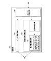
図10は、異なるライン幅および異なるライン間隔のラインパターンが形成された試料10の一例を示す。試料10は、第1の部分、第2の部分、および第3の部分を有し、それぞれの部分において異なるライン幅および異なるライン間隔のラインパターンが形成された例を示す。このように、複数の種類のラインパターンが1つの試料に形成される場合であっても、それぞれのラインパターンは、共通のグリッドを用いて設計されたものとする。   FIG. 10 shows an example of the sample 10 in which line patterns having different line widths and different line intervals are formed. Sample 10 has a first portion, a second portion, and a third portion, and shows an example in which line patterns having different line widths and different line intervals are formed in the respective portions. Thus, even when a plurality of types of line patterns are formed on one sample, each line pattern is designed using a common grid.

図10は、第1の部分のラインパターン802は、ライン幅およびライン間隔がgであり、第2の部分のラインパターン804は、ライン幅が2g、ライン間隔がgであり、第3の部分のラインパターン806は、ライン幅が3g、ライン間隔が2gである例を示す。   In FIG. 10, the line width and line interval of the first part line pattern 802 is g, and the line pattern 804 of the second part is 2 g line width and g is the third part. The line pattern 806 shows an example in which the line width is 3 g and the line interval is 2 g.

このように、ラインパターンの幅および間隔が異なると、それぞれのラインパターンに対応するカットパターン810、820、830の大きさもそれぞれ異なることになる。しかしながら、ラインパターンのそれぞれが、同一のグリッド800に基づいて設計されている場合、それぞれのカットパターンのY座標は、図4および図5で説明したように、当該グリッド800の離散した座標で表すことができる。この場合、本実施形態の露光装置100は、電子ビームの照射位置を間隔gのグリッド対応させているので、このようなカットパターンであっても露光することができる。   Thus, when the width and interval of the line patterns are different, the sizes of the cut patterns 810, 820, and 830 corresponding to the respective line patterns are also different. However, when each of the line patterns is designed based on the same grid 800, the Y coordinate of each cut pattern is represented by discrete coordinates of the grid 800 as described with reference to FIGS. be able to. In this case, since the exposure apparatus 100 of the present embodiment associates the irradiation position of the electron beam with the grid of the interval g, exposure can be performed even with such a cut pattern.

図11は、本実施形態に係る電子ビームの照射領域502を、グリッド800に対応させて配置した例を示す。即ち、図11は、図5で説明したように、−Y方向側から数えてn番目に配置する電子ビームBnの照射領域が、−Y方向側から数えてn番目とn+1番目のグリッドの間に位置する例を示す。これによって、例えば、カットパターンがk番目とl(エル)番目のグリッドの間に位置する場合、露光装置100は、k番目から(l−1)番目までの電子ビームを用いることで、当該カットパターンを露光することができる。   FIG. 11 shows an example in which the electron beam irradiation area 502 according to the present embodiment is arranged in correspondence with the grid 800. That is, in FIG. 11, as described in FIG. 5, the irradiation region of the electron beam Bn arranged nth from the −Y direction side is between the nth and n + 1th grids counted from the −Y direction side. An example located in Thereby, for example, when the cut pattern is located between the kth and l (el) grids, the exposure apparatus 100 uses the kth to (l-1) th electron beams to thereby cut the cut pattern. The pattern can be exposed.

即ち、この場合、選択部160は、指定された照射位置におけるラインパターンの幅に応じて、複数の荷電粒子ビームのうち幅方向に連続する少なくとも1つの荷電粒子ビームを選択する。選択部160は、例えば、第1の部分のラインパターン802のライン幅gに応じて、当該ラインパターン802をカットするパターン幅2gのカットパターンを露光すべく、アレイビームのうち幅方向に並ぶ2つの電子ビームを選択する。   That is, in this case, the selection unit 160 selects at least one charged particle beam that is continuous in the width direction from among the plurality of charged particle beams according to the width of the line pattern at the designated irradiation position. For example, the selection unit 160 arranges 2 in the array beam in the width direction so as to expose a cut pattern having a pattern width 2g for cutting the line pattern 802 in accordance with the line width g of the line pattern 802 of the first portion. Select one electron beam.

また、選択部160は、例えば、第2の部分のラインパターン804のライン幅2gに応じて、当該ラインパターン804をカットするパターン幅3gのカットパターンを露光すべく、アレイビームのうち幅方向に並ぶ3つの電子ビームを選択する。同様に、選択部160は、第3の部分のラインパターン806のライン幅3gに応じて、当該ラインパターン806をカットするパターン幅4gのカットパターンを露光すべく、アレイビームのうち幅方向に並ぶ4つの電子ビームを選択する。このように、選択部160は、m×gのライン幅に応じて、(m+1)個の電子ビームを選択する。   Further, the selection unit 160, for example, in the width direction of the array beam in order to expose a cut pattern having a pattern width 3g for cutting the line pattern 804 in accordance with the line width 2g of the line pattern 804 of the second portion. Select three electron beams side by side. Similarly, the selection unit 160 is arranged in the width direction of the array beam so as to expose a cut pattern having a pattern width of 4 g for cutting the line pattern 806 according to the line width 3 g of the line pattern 806 of the third portion. Four electron beams are selected. As described above, the selection unit 160 selects (m + 1) electron beams according to the m × g line width.

また、選択部160は、図6および図7で説明したように、選択した電子ビームに対応する経過時間を決定して照射位置をそれぞれ検出する。これによって、露光制御部140は、アレイビーム500の照射位置を走査しつつ、電子ビームの照射を制御することで、カットパターン810、820、および830をそれぞれ露光することができる。なお、図11の例においても、露光装置100は、電子ビームの数nに応じたビーム幅n×gのアレイビームを走査し、当該ビーム幅n×gに相当するフレーム幅を有するフレーム毎に試料10を露光してよい。これによって、本実施形態に係る露光装置100は、試料10に異なるライン幅および異なるライン間隔のラインパターンが形成されても、照射位置に対応して適切な電子ビームを選択することにより、対応するカットパターンを露光することができる。   Further, as described with reference to FIGS. 6 and 7, the selection unit 160 determines the elapsed time corresponding to the selected electron beam and detects the irradiation position. Accordingly, the exposure control unit 140 can expose the cut patterns 810, 820, and 830 by controlling the irradiation of the electron beam while scanning the irradiation position of the array beam 500, respectively. In the example of FIG. 11 as well, the exposure apparatus 100 scans an array beam having a beam width n × g corresponding to the number n of electron beams, and each frame having a frame width corresponding to the beam width n × g. The sample 10 may be exposed. Thereby, the exposure apparatus 100 according to the present embodiment can cope with the case where line patterns having different line widths and different line intervals are formed on the sample 10 by selecting an appropriate electron beam corresponding to the irradiation position. The cut pattern can be exposed.

以上の本実施形態に係る露光装置100は、経過時間に応じたカットパターンの領域において、選択部160が選択した電子ビームを試料10に照射することを説明した。これに加えて、露光装置100は、電子ビームを照射する制御信号を調節して、カットパターンの領域内の露光量を調整してよい。即ち、照射制御部170は、少なくとも1つの荷電粒子ビームをラインパターンの長手方向に沿って指定された長さの範囲に照射する場合において、当該少なくとも1つの荷電粒子ビームの照射量を当該範囲内における照射位置に応じて変更する。   The exposure apparatus 100 according to the present embodiment described above irradiates the sample 10 with the electron beam selected by the selection unit 160 in the cut pattern region corresponding to the elapsed time. In addition to this, the exposure apparatus 100 may adjust the exposure amount in the area of the cut pattern by adjusting the control signal for irradiating the electron beam. That is, in the case where the irradiation control unit 170 irradiates at least one charged particle beam to a range of a specified length along the longitudinal direction of the line pattern, the irradiation amount of the at least one charged particle beam falls within the range. It changes according to the irradiation position.

図12は、本実施形態に係る照射制御部170が生成したカットパターンの露光量を調節する制御信号の一例を示す。図12は、図7と同様に、横軸は時間、縦軸は電圧を示す。時点T7において、電子ビームB2およびB4を試料10に照射すべく、制御信号B2およびB4は、ハイ状態からロー状態に切り替わる。また、時点T9において、電子ビームB2およびB4の照射を停止すべく、制御信号B2およびB4は、ロー状態からハイ状態に切り替わる。   FIG. 12 shows an example of a control signal for adjusting the exposure amount of the cut pattern generated by the irradiation control unit 170 according to this embodiment. In FIG. 12, as in FIG. 7, the horizontal axis indicates time, and the vertical axis indicates voltage. At time T7, the control signals B2 and B4 are switched from the high state to the low state in order to irradiate the sample 10 with the electron beams B2 and B4. At time T9, the control signals B2 and B4 are switched from the low state to the high state in order to stop the irradiation of the electron beams B2 and B4.

同様に、時点T8おいて、電子ビームB1およびB3を試料10に照射すべく、制御信号B1およびB3は、ハイ状態からロー状態に切り替わり、時点T10において、電子ビームB1およびB3の照射を停止すべく、制御信号B1およびB3は、ロー状態からハイ状態に切り替わる。ここで、時点T7とT8の時間差、および時点T9とT10の時間差は、共に電子ビームの列の間隔δに応じた時間差(δ/V)に略等しい。これによって、電子ビームB1からB4は、X軸において略同一座標で照射が開始され、略同一座標で照射が停止される。即ち、例えば、電子ビームB1からB4は、図11におけるカットパターン832を露光するように駆動される。   Similarly, the control signals B1 and B3 are switched from the high state to the low state to irradiate the sample 10 with the electron beams B1 and B3 at time T8, and the irradiation of the electron beams B1 and B3 is stopped at time T10. Therefore, the control signals B1 and B3 are switched from the low state to the high state. Here, the time difference between time points T7 and T8 and the time difference between time points T9 and T10 are both substantially equal to the time difference (δ / V) according to the interval δ of the electron beam column. As a result, the irradiation of the electron beams B1 to B4 is started at substantially the same coordinate on the X axis, and is stopped at substantially the same coordinate. That is, for example, the electron beams B1 to B4 are driven so as to expose the cut pattern 832 in FIG.

このように、複数の電子ビームを用いてカットパターンを露光する場合、露光領域の露光面積が大きければ大きいほど、当該露光領域の境界が不明瞭にぼやける傾向が生じることがある。そこで、本実施形態の露光装置100は、電子ビームを照射する制御信号を調節して露光量を低減させ、露光領域の境界が不明瞭となることを低減してよい。   As described above, when a cut pattern is exposed using a plurality of electron beams, the larger the exposure area of the exposure area, the more likely the boundary of the exposure area becomes unclearly blurred. Therefore, the exposure apparatus 100 of the present embodiment may reduce the exposure amount by adjusting the control signal for irradiating the electron beam, and reduce the unclearness of the boundary of the exposure region.

即ち、照射制御部170は、少なくとも1つの荷電粒子ビームをラインパターンの長手方向に沿って指定された長さの範囲に照射する場合において、少なくとも1つの荷電粒子ビームを試料10に照射するか否かを当該範囲内における照射位置に応じて変更する。例えば、照射制御部170は、電子ビームB2およびB4を試料10に照射して露光する時点T7から時点T9の間の期間において、当該電子ビームB2およびB4の照射と停止を繰り返す。同様に、照射制御部170は、電子ビームB1およびB3を試料10に照射して露光する時点T8から時点T10の間の期間において、当該電子ビームB1およびB3の照射と停止を繰り返す。   That is, the irradiation control unit 170 determines whether or not to irradiate the sample 10 with at least one charged particle beam when irradiating at least one charged particle beam to a specified length range along the longitudinal direction of the line pattern. Is changed according to the irradiation position within the range. For example, the irradiation control unit 170 repeats irradiation and stopping of the electron beams B2 and B4 in a period between the time T7 and the time T9 when the sample 10 is irradiated with the electron beams B2 and B4 and exposed. Similarly, the irradiation control unit 170 repeats irradiation and stopping of the electron beams B1 and B3 in a period between the time T8 and the time T10 when the sample 10 is irradiated with the electron beams B1 and B3 for exposure.

このように、照射制御部170は、電子ビームを照射して露光する期間において、電子ビームの照射を停止する期間を設けることにより、露光領域全体の露光量を調節することができる。ここで、照射制御部170は、複数の荷電粒子ビームのうち、経路が最も近接する2つの荷電粒子ビームの試料10に照射するタイミングをずらしてよい。例えば、照射制御部170は、露光する期間において、電子ビームB1の照射を停止する期間と、電子ビームB2の照射を停止する期間とが時間的に重ならないように制御する。これによって、照射制御部170は、露光量域内において、電子ビームが照射されない位置を分散させることができ、電子ビームの照射量が部分的に偏ることを防止する。   As described above, the irradiation control unit 170 can adjust the exposure amount of the entire exposure region by providing the period for stopping the irradiation of the electron beam in the period for performing the irradiation by irradiating the electron beam. Here, the irradiation control unit 170 may shift the timing of irradiating the sample 10 of the two charged particle beams whose paths are closest to each other among the plurality of charged particle beams. For example, in the exposure period, the irradiation control unit 170 performs control so that the period during which the irradiation with the electron beam B1 is stopped does not overlap with the period during which the irradiation with the electron beam B2 is stopped. Accordingly, the irradiation control unit 170 can disperse the positions where the electron beam is not irradiated within the exposure amount region, and prevents the electron beam irradiation amount from being partially biased.

図13は、図12に示すタイミングチャートに示す露光量制御を実行する選択部160の構成例を示す。図13において、図6に示された本実施形態に係る選択部160の動作と略同一のものには同一の符号を付け、説明を省略する。図13に示す経過時間演算回路166は、露光量調整回路168を更に含み、ビーム選択回路164が選択した電子ビームをON状態およびOFF状態にすべき経過時間を検出することに加え、露光量を制御するための経過時間を算出する。   FIG. 13 shows a configuration example of the selection unit 160 that executes the exposure amount control shown in the timing chart shown in FIG. In FIG. 13, the same reference numerals are given to substantially the same operations as those of the selection unit 160 according to the present embodiment illustrated in FIG. 6, and description thereof is omitted. The elapsed time calculation circuit 166 shown in FIG. 13 further includes an exposure amount adjustment circuit 168. In addition to detecting the elapsed time during which the electron beam selected by the beam selection circuit 164 is to be turned on and off, the exposure amount is calculated. The elapsed time for control is calculated.

経過時間演算回路166は、例えば、図12に示すように、4つの電子ビームB1,B2,B3,B4をON状態およびOFF状態にすべき経過時間(DL1a,DL2a,DL3a,DL4a,DL1b,DL2b,DL3b,DL4b)を、(数1)および(数2)式を用いて算出する。そして、露光量調整回路168は、ON状態にすべき経過時間からOFF状態にすべき経過時間の間の期間において、更にON状態およびOFF状態にして露光量を調整する経過時間を算出する。露光量を調整する経過時間をDL11,DL12,DL13,・・・等とすると、以下の関係式を満たす。
(数3)
DL1a<DL11<DL12<DL13<・・・<DL1b
DL2a<DL21<DL22<DL23<・・・<DL2b
DL3a<DL31<DL32<DL33<・・・<DL3b
DL4a<DL41<DL42<DL43<・・・<DL4b
For example, as shown in FIG. 12, the elapsed time calculation circuit 166 has elapsed times (DL1a, DL2a, DL3a, DL4a, DL1b, DL2b) in which the four electron beams B1, B2, B3, B4 should be turned on and off. , DL3b, DL4b) are calculated using the formulas (1) and (2). Then, the exposure adjustment circuit 168 calculates an elapsed time for adjusting the exposure in the ON state and the OFF state in a period between the elapsed time to be turned on and the elapsed time to be turned off. If the elapsed time for adjusting the exposure amount is DL11, DL12, DL13,..., The following relational expression is satisfied.
(Equation 3)
DL1a <DL11 <DL12 <DL13 <... <DL1b
DL2a <DL21 <DL22 <DL23 <... <DL2b
DL3a <DL31 <DL32 <DL33 <... <DL3b
DL4a <DL41 <DL42 <DL43 <... <DL4b

露光量を調整する経過時間は、レジストの材料等にも依存するので、露光装置100は、露光量に対する露光領域の境界の状態を予め観測し、適切な露光量となる条件を記憶部150等に記憶することが望ましい。これに代えて、ユーザがCPU130等を用いて、露光量を調整する経過時間に対応するパラメータ等を入力してもよい。これにより、経過時間演算回路166は、露光領域の境界の状態を調節する経過時間を算出することができる。   Since the elapsed time for adjusting the exposure amount also depends on the resist material and the like, the exposure apparatus 100 observes in advance the state of the boundary of the exposure region with respect to the exposure amount, and sets conditions for an appropriate exposure amount, such as the storage unit 150 It is desirable to memorize. Instead, the user may input parameters or the like corresponding to the elapsed time for adjusting the exposure amount using the CPU 130 or the like. Thereby, the elapsed time calculation circuit 166 can calculate the elapsed time for adjusting the boundary state of the exposure region.

以上の本実施形態に係る露光装置100は、ブランキング部60において、ブランキング電極64に供給される電圧に応じて電子ビームを偏向するか否かを切り換えることを説明した。このような機能を有するブランキング部60の一例について、図14を用いて説明する。   In the above exposure apparatus 100 according to the present embodiment, it has been described that the blanking unit 60 switches whether to deflect the electron beam according to the voltage supplied to the blanking electrode 64. An example of the blanking unit 60 having such a function will be described with reference to FIG.

図14は、本実施形態に係るブランキング部60の一例を示す。ブランキング部60は、複数の開口62と、第1のブランキング電極64aと、第2のブランキング電極64bと、共通電極66と、電極配線68とを有する。   FIG. 14 shows an example of the blanking unit 60 according to the present embodiment. The blanking unit 60 includes a plurality of openings 62, a first blanking electrode 64 a, a second blanking electrode 64 b, a common electrode 66, and an electrode wiring 68.

複数の開口62は、複数の荷電粒子ビームのそれぞれを個別に通過させる。即ち、複数の開口62は、ビームアレイとして出力する複数の電子ビームに対応した数がブランキング部60に設けられることが望ましい。図14において、複数の開口62は、ラインパターンの長手方向に対応する向きであるX方向において、第1の開口62aと第2の開口62bに分けて示す。第1の開口62aは、−X方向側において、Y方向に並ぶ複数の開口62であり、例えば、図5における電子ビームB1、B3、B5、およびB7に対応して形成される。第2の開口62bは、+X方向側において、Y方向に並ぶ複数の開口62であり、例えば、図5における電子ビームB2、B4、B6、およびB8に対応して形成される。   The plurality of openings 62 allow each of the plurality of charged particle beams to pass individually. That is, it is desirable that the plurality of openings 62 be provided in the blanking unit 60 in a number corresponding to the plurality of electron beams output as a beam array. In FIG. 14, the plurality of openings 62 are divided into a first opening 62 a and a second opening 62 b in the X direction, which is the direction corresponding to the longitudinal direction of the line pattern. The first openings 62a are a plurality of openings 62 arranged in the Y direction on the −X direction side, and are formed, for example, corresponding to the electron beams B1, B3, B5, and B7 in FIG. The second openings 62b are a plurality of openings 62 arranged in the Y direction on the + X direction side, and are formed, for example, corresponding to the electron beams B2, B4, B6, and B8 in FIG.

第1のブランキング電極64aは、第1の開口62aにおける共通電極66とは反対側の壁面に設けられる。第2のブランキング電極64bは、第2の開口62bにおける共通電極66とは反対側の壁面に設けられる。共通電極66は、X方向において、第1の開口62aおよび第2の開口62bの間の壁面に設けられた、第1の開口62aおよび第2の開口62bに共通の電極である。また、共通電極66は、Y方向に並ぶ複数の開口62のうち隣り合う開口62の間にそれぞれ設けられてよい。   The first blanking electrode 64a is provided on the wall surface of the first opening 62a opposite to the common electrode 66. The second blanking electrode 64b is provided on the wall surface opposite to the common electrode 66 in the second opening 62b. The common electrode 66 is an electrode common to the first opening 62a and the second opening 62b provided on the wall surface between the first opening 62a and the second opening 62b in the X direction. Further, the common electrode 66 may be provided between adjacent openings 62 among the plurality of openings 62 arranged in the Y direction.

電極配線68は、第1のブランキング電極64aおよび第2のブランキング電極64bのそれぞれと、照射制御部170とを対応する増幅器172を介して接続する。照射制御部170は、選択部160による選択に応じて第1のブランキング電極64aおよび第2のブランキング電極64bの電圧を変更し、電子ビームのON状態およびOFF状態をそれぞれ切り換える。   The electrode wiring 68 connects each of the first blanking electrode 64a and the second blanking electrode 64b to the irradiation control unit 170 via a corresponding amplifier 172. The irradiation control unit 170 changes the voltages of the first blanking electrode 64a and the second blanking electrode 64b according to the selection by the selection unit 160, and switches the ON state and the OFF state of the electron beam, respectively.

以上のように、ブランキング部60は、Y方向に2列に並ぶ複数の開口62を有するので、共通電極66で複数の開口62のそれぞれを分離しつつ、当該複数の開口62のY座標における配置を連続して配置させることができる。これにより、照射制御部170は、複数の開口62のそれぞれに対応するブランキング電極に、電子ビームのON状態およびOFF状態をそれぞれ切り換える電圧を個別に供給して、個別に制御することができる。また、複数の開口62を通過する複数の電子ビームは、照射領域のY座標を連続させたアレイビームにすることができる。即ち、当該アレイビームの1回の走査により、Y座標における連続した電子ビーム照射の範囲をフレーム幅とするX軸方向に延伸するフレームを、当該アレイビームの照射可能領域とすることができる。   As described above, since the blanking section 60 has the plurality of openings 62 arranged in two rows in the Y direction, the plurality of openings 62 are separated by the common electrode 66 while the plurality of openings 62 are in the Y coordinate. The arrangement can be arranged continuously. Thereby, the irradiation controller 170 can individually control the blanking electrodes corresponding to the plurality of openings 62 by individually supplying voltages for switching the ON state and the OFF state of the electron beam. Further, the plurality of electron beams that pass through the plurality of openings 62 can be array beams in which the Y coordinates of the irradiation region are continuous. In other words, a frame extending in the X-axis direction with a continuous electron beam irradiation range in the Y coordinate as a frame width by one scan of the array beam can be set as the array beam irradiable region.

以上の本実施形態に係るブランキング部60は、Y方向に2列に並ぶ複数の開口62を有することを説明したが、これに代えて、ブランキング部60は、Y方向に3列以上に並ぶ複数の開口62を有してもよい。この場合においても、共通電極66で複数の開口62のそれぞれを分離しつつ、当該複数の開口62のY座標における配置を連続して配置させることができるので、カラム部120は、フレーム毎にアレイビームを走査して試料10の表面を露光することができる。   Although it has been described that the blanking portion 60 according to the present embodiment has a plurality of openings 62 arranged in two rows in the Y direction, the blanking portion 60 is arranged in three or more rows in the Y direction instead. A plurality of openings 62 may be arranged. Also in this case, the plurality of openings 62 can be continuously arranged in the Y coordinate while separating each of the plurality of openings 62 by the common electrode 66, so that the column unit 120 is arranged in an array for each frame. The surface of the sample 10 can be exposed by scanning the beam.

以上の本実施形態に係る露光装置100は、1つのカラム部120を備えるシングルカラムタイプの電子ビーム露光装置として説明したが、これに限定されるものではなく、露光装置100は、複数のカラム部120を備えてもよい。このような複数のカラム部120を備える露光装置100について、図15を用いて説明する。   The exposure apparatus 100 according to this embodiment has been described as a single column type electron beam exposure apparatus including one column unit 120. However, the present invention is not limited to this, and the exposure apparatus 100 includes a plurality of column units. 120 may be provided. An exposure apparatus 100 including such a plurality of column units 120 will be described with reference to FIG.

図15は、本実施形態に係る露光装置100の変形例を示す。図15において、図1に示された本実施形態に係る露光装置100の動作と略同一のものには同一の符号を付け、説明を省略する。本変形例の露光装置100は、カラム部120と、選択部160、照射制御部170、および偏向量決定部180を有する露光制御部140とを複数備える。   FIG. 15 shows a modification of the exposure apparatus 100 according to this embodiment. In FIG. 15, substantially the same operations as those of the exposure apparatus 100 according to the present embodiment shown in FIG. The exposure apparatus 100 of this modification includes a plurality of exposure control units 140 including a column unit 120, a selection unit 160, an irradiation control unit 170, and a deflection amount determination unit 180.

なお、本変形例の露光装置100において、ステージ装置112を移動させてアレイビームの照射位置を走査する場合、露光制御部140のそれぞれは、走査制御部190を有さなくてもよい。図15は、1つのステージ部110と、露光装置100が複数のカラム部120と、1つのCPU130と、走査制御部190を有さない複数の露光制御部140と、1つの走査制御部190とを備える例を示す。   In the exposure apparatus 100 of the present modification, when the stage apparatus 112 is moved to scan the irradiation position of the array beam, each of the exposure control units 140 may not have the scanning control unit 190. In FIG. 15, one stage unit 110, the exposure apparatus 100 includes a plurality of column units 120, a single CPU 130, a plurality of exposure control units 140 that do not include the scan control unit 190, and a single scan control unit 190. An example comprising:

複数のカラム部120のそれぞれは、対応する露光制御部140にそれぞれ接続され、試料10を露光する。個々のカラム部120の動作は、図3等で説明したように、照射可能領域200をフレーム毎に露光する。即ち、走査制御部190は、試料10を載置して移動させるステージ部110を制御して複数のカラム部120に対して試料10を移動させ、複数のカラム部120によって並列に試料10に荷電粒子ビームを照射する。   Each of the plurality of column units 120 is connected to the corresponding exposure control unit 140 to expose the sample 10. The operation of each column unit 120 exposes the irradiable region 200 for each frame, as described with reference to FIG. That is, the scanning control unit 190 controls the stage unit 110 on which the sample 10 is placed and moved to move the sample 10 with respect to the plurality of column units 120, and charges the sample 10 in parallel by the plurality of column units 120. Irradiate a particle beam.

このように、本変形例の電子ビーム露光装置100は、複数本のカラム部120で並行して露光を行うことができるため、露光のスループットを大幅に向上させることができる。また、試料10が300mmを超える大口径の半導体ウエハ等であっても、対応してカラム部120の数を増加させることで、スループットが著しく低下することを防止できる。   As described above, since the electron beam exposure apparatus 100 according to the present modification can perform exposure in parallel with the plurality of column sections 120, the throughput of exposure can be significantly improved. Further, even if the sample 10 is a semiconductor wafer having a large diameter exceeding 300 mm, the throughput can be prevented from being significantly lowered by correspondingly increasing the number of column portions 120.

なお、本変形例の露光装置100は、複数のカラム部120が出力する複数のアレイビームの強度がそれぞれ異なる場合がある。そこで、露光装置100は、露光を行う前に、それぞれのカラム部120から出力されるアレイビームの強度を予め測定してよい。また、複数のカラム部120による複数の露光結果にバラつきが生じないように、各露光制御部140における経過時間を補正してもよい。また、複数のカラム部120が、1つの試料10上の異なる半導体チップに属するカットパターンをそれぞれ露光するように、カラム部120毎に、アレイビームと当該アレイビームが露光するチップのラインパターンとを位置決めしてもよい。   In the exposure apparatus 100 of this modification, the intensity of the plurality of array beams output from the plurality of column units 120 may be different from each other. Therefore, the exposure apparatus 100 may measure in advance the intensity of the array beam output from each column unit 120 before performing exposure. Further, the elapsed time in each exposure control unit 140 may be corrected so that a plurality of exposure results from the plurality of column units 120 do not vary. Further, an array beam and a line pattern of a chip exposed by the array beam are provided for each column unit 120 so that a plurality of column units 120 respectively expose cut patterns belonging to different semiconductor chips on one sample 10. You may position.

以上、本発明を実施の形態を用いて説明したが、本発明の技術的範囲は上記実施の形態に記載の範囲には限定されない。上記実施の形態に、多様な変更または改良を加えることが可能であることが当業者に明らかである。その様な変更または改良を加えた形態も本発明の技術的範囲に含まれ得ることが、特許請求の範囲の記載から明らかである。   As mentioned above, although this invention was demonstrated using embodiment, the technical scope of this invention is not limited to the range as described in the said embodiment. It will be apparent to those skilled in the art that various modifications or improvements can be added to the above-described embodiment. It is apparent from the scope of the claims that the embodiments added with such changes or improvements can be included in the technical scope of the present invention.

特許請求の範囲、明細書、および図面中において示した装置、システム、プログラム、および方法における動作、手順、ステップ、および段階等の各処理の実行順序は、特段「より前に」、「先立って」等と明示しておらず、また、前の処理の出力を後の処理で用いるのでない限り、任意の順序で実現しうることに留意すべきである。特許請求の範囲、明細書、および図面中の動作フローに関して、便宜上「まず、」、「次に、」等を用いて説明したとしても、この順で実施することが必須であることを意味するものではない。   The order of execution of each process such as operations, procedures, steps, and stages in the apparatus, system, program, and method shown in the claims, the description, and the drawings is particularly “before” or “prior to”. It should be noted that the output can be realized in any order unless the output of the previous process is used in the subsequent process. Regarding the operation flow in the claims, the description, and the drawings, even if it is described using “first”, “next”, etc. for convenience, it means that it is essential to carry out in this order. It is not a thing.

10 試料、20 電子銃、30 アパーチャプレート、32 開口、40 ビーム形状変形部、50 アパーチャアレイ、52 開口、60 ブランキング部、62 開口、62a 第1の開口、62b 第2の開口、64 ブランキング電極、64a 第1のブランキング電極、64b 第2のブランキング電極、66 共通電極、68 電極配線、70 ストッピングプレート、72 開口、80 調整部、90 外部記憶部、100 露光装置、110 ステージ部、112 ステージ装置、114 ステージ位置検出部、120 カラム部、130 CPU、132 バス、140 露光制御部、150 記憶部、160 選択部、162 データ変換回路、164 ビーム選択回路、166 経過時間演算回路、168 露光量調整回路、170 照射制御部、172 増幅器、180 偏向量決定部、182 偏向部駆動回路、190 走査制御部、192 ステージ駆動回路、200 照射可能領域、210 照射位置、220 領域、232 第1フレーム、234 第2フレーム、236 第3フレーム、400 グリッド、402 ラインパターン、410 第1パターン、412、414、416、418 パターン、420 第2パターン、422、424 パターン、430 第3パターン、432、434、436、438 パターン、500 アレイビーム、502 照射領域、800 グリッド、802、804、806 ラインパターン、810、820、830、832 カットパターン、900 配線パターン 10 sample, 20 electron gun, 30 aperture plate, 32 aperture, 40 beam shape deformed portion, 50 aperture array, 52 aperture, 60 blanking portion, 62 aperture, 62a first aperture, 62b second aperture, 64 blanking Electrode, 64a first blanking electrode, 64b second blanking electrode, 66 common electrode, 68 electrode wiring, 70 stopping plate, 72 opening, 80 adjustment unit, 90 external storage unit, 100 exposure apparatus, 110 stage unit 112 stage device, 114 stage position detection unit, 120 column unit, 130 CPU, 132 bus, 140 exposure control unit, 150 storage unit, 160 selection unit, 162 data conversion circuit, 164 beam selection circuit, 166 elapsed time calculation circuit, 168 Exposure adjustment circuit, 170 Irradiation system Control unit, 172 amplifier, 180 deflection amount determination unit, 182 deflection unit drive circuit, 190 scanning control unit, 192 stage drive circuit, 200 irradiable region, 210 irradiation position, 220 region, 232 first frame, 234 second frame, 236 3rd frame, 400 grid, 402 line pattern, 410 1st pattern, 412, 414, 416, 418 pattern, 420 2nd pattern, 422, 424 pattern, 430 3rd pattern, 432, 434, 436, 438 pattern, 500 array beam, 502 irradiation area, 800 grid, 802, 804, 806 line pattern, 810, 820, 830, 832 cut pattern, 900 wiring pattern

Claims (13)

試料上のラインパターンに応じた位置に荷電粒子ビームを照射する露光装置であって、
前記ラインパターンの幅方向に照射位置が異なる複数の荷電粒子ビームを発生するビーム発生部と、
前記複数の荷電粒子ビームの照射位置を、前記ラインパターンの長手方向に沿って走査させる走査制御部と、
前記ラインパターン上の長手方向の指定された照射位置において、前記複数の荷電粒子ビームのうち前記試料に照射すべき少なくとも1つの荷電粒子ビームを選択する選択部と、
選択された前記少なくとも1つの荷電粒子ビームを前記試料へと照射する制御をする照射制御部と、
を備える露光装置。
An exposure apparatus that irradiates a charged particle beam at a position corresponding to a line pattern on a sample,
A beam generator for generating a plurality of charged particle beams having different irradiation positions in the width direction of the line pattern;
A scanning control unit that scans irradiation positions of the plurality of charged particle beams along a longitudinal direction of the line pattern;
A selection unit that selects at least one charged particle beam to be irradiated on the sample among the plurality of charged particle beams at a designated irradiation position in a longitudinal direction on the line pattern;
An irradiation control unit that controls to irradiate the sample with the selected at least one charged particle beam;
An exposure apparatus comprising:
前記選択部は、前記指定された照射位置における前記ラインパターンの幅に応じて、前記複数の荷電粒子ビームのうち幅方向に連続する前記少なくとも1つの荷電粒子ビームを選択する請求項1に記載の露光装置。   2. The selection unit according to claim 1, wherein the selection unit selects the at least one charged particle beam that is continuous in a width direction among the plurality of charged particle beams according to a width of the line pattern at the designated irradiation position. Exposure device. 前記試料を載置して移動させるステージ部を更に備え、
前記走査制御部は、前記荷電粒子ビームの通過経路を維持した状態で前記ステージ部によって前記試料を前記ラインパターンの長手方向へと移動させる
請求項1または2に記載の露光装置。
It further comprises a stage part for placing and moving the sample,
The exposure apparatus according to claim 1, wherein the scanning control unit moves the sample in the longitudinal direction of the line pattern by the stage unit while maintaining a passage path of the charged particle beam.
前記複数の荷電粒子ビームを偏向する偏向部を更に備え、
前記走査制御部は、前記ステージ部による前記試料の移動誤差に応じて前記荷電粒子ビームの通過経路を調整する請求項3に記載の露光装置。
A deflection unit for deflecting the plurality of charged particle beams;
The exposure apparatus according to claim 3, wherein the scanning control unit adjusts a passage path of the charged particle beam according to a movement error of the sample by the stage unit.
前記選択部は、前記複数の荷電粒子ビームの照射位置が前記ラインパターンの長手方向における予め定められた基準位置を経過してからの経過時間に応じて前記指定された照射位置を検出する請求項1から4のいずれか一項に記載の露光装置。   The said selection part detects the said designated irradiation position according to the elapsed time after the irradiation position of these charged particle beams passed the predetermined reference position in the longitudinal direction of the said line pattern. The exposure apparatus according to any one of 1 to 4. 前記選択部は、前記複数の荷電粒子ビームの照射位置が前記ラインパターンの長手方向における複数の基準位置のうち最後に経過した基準位置と、当該基準位置を経過してからの経過時間とに応じて、前記指定された照射位置を検出する請求項5に記載の露光装置。   The selection unit is responsive to a reference position at which the irradiation position of the plurality of charged particle beams last among a plurality of reference positions in the longitudinal direction of the line pattern and an elapsed time since the reference position has passed. The exposure apparatus according to claim 5, wherein the designated irradiation position is detected. 前記照射制御部は、前記少なくとも1つの荷電粒子ビームを前記ラインパターンの長手方向に沿って指定された長さの範囲に照射する場合において、前記少なくとも1つの荷電粒子ビームの照射量を当該範囲内における照射位置に応じて変更する請求項1から6のいずれか一項に記載の露光装置。   In the case where the irradiation control unit irradiates the at least one charged particle beam in a range of a length specified along the longitudinal direction of the line pattern, the irradiation amount of the at least one charged particle beam falls within the range. The exposure apparatus according to any one of claims 1 to 6, wherein the exposure apparatus is changed according to the irradiation position. 前記照射制御部は、前記少なくとも1つの荷電粒子ビームを前記試料に照射するか否かを当該範囲内における照射位置に応じて変更する請求項7に記載の露光装置。   The exposure apparatus according to claim 7, wherein the irradiation control unit changes whether to irradiate the sample with the at least one charged particle beam according to an irradiation position within the range. 前記照射制御部は、前記複数の荷電粒子ビームのうち、経路が最も近接する2つの荷電粒子ビームの前記試料に照射するタイミングをずらす請求項8に記載の露光装置。   The exposure apparatus according to claim 8, wherein the irradiation control unit shifts the timing of irradiating the sample with the two charged particle beams having the closest paths among the plurality of charged particle beams. 前記複数の荷電粒子ビームのそれぞれを前記試料に照射させるか否かを切り替えるブランキング部を更に備え、
前記ブランキング部は、
前記複数の荷電粒子ビームのそれぞれを個別に通過させる複数の開口と、
前記ラインパターンの長手方向に対応する向きにおいて第1の前記開口および第2の前記開口の間の壁面に設けられた、前記第1の開口および前記第2の開口に共通の共通電極と、
前記第1の開口における前記共通電極とは反対側の壁面に設けられた、第1のブランキング電極と、
前記第2の開口における前記共通電極とは反対側の壁面に設けられた、第2のブランキング電極と、
を有する請求項1から9のいずれか一項に記載の露光装置。
A blanking section for switching whether to irradiate the sample with each of the plurality of charged particle beams;
The blanking part
A plurality of apertures for individually passing each of the plurality of charged particle beams;
A common electrode provided on a wall surface between the first opening and the second opening in a direction corresponding to the longitudinal direction of the line pattern, and common to the first opening and the second opening;
A first blanking electrode provided on a wall surface of the first opening opposite to the common electrode;
A second blanking electrode provided on a wall surface of the second opening opposite to the common electrode;
An exposure apparatus according to any one of claims 1 to 9, wherein:
前記照射制御部は、前記選択部による選択に応じて前記第1のブランキング電極および前記第2のブランキング電極の電圧を変更する請求項10に記載の露光装置。   The exposure apparatus according to claim 10, wherein the irradiation control unit changes the voltages of the first blanking electrode and the second blanking electrode in accordance with selection by the selection unit. 前記ビーム発生部、前記選択部、および前記照射制御部を複数備え、
前記走査制御部は、前記試料を載置して移動させるステージ部を制御して複数の前記ビーム発生部に対して前記試料を移動させ、
前記複数のビーム発生部によって並列に前記試料に荷電粒子ビームを照射する
請求項1から11のいずれか一項に記載の露光装置。
A plurality of the beam generation unit, the selection unit, and the irradiation control unit,
The scanning control unit controls the stage unit on which the sample is placed and moved to move the sample with respect to the plurality of beam generation units,
The exposure apparatus according to claim 1, wherein the sample is irradiated with a charged particle beam in parallel by the plurality of beam generation units.
試料上のラインパターンに応じた位置に荷電粒子ビームを照射する露光方法であって、
前記ラインパターンの幅方向に照射位置が異なる複数の荷電粒子ビームを発生するビーム発生段階と、
前記複数の荷電粒子ビームの照射位置を、前記ラインパターンの長手方向に沿って走査させる走査制御段階と、
前記ラインパターン上の長手方向の指定された照射位置において、前記複数の荷電粒子ビームのうち前記試料に照射すべき少なくとも1つの荷電粒子ビームを選択する選択段階と、
選択された前記少なくとも1つの荷電粒子ビームを前記試料へと照射する制御をする照射制御段階と、
を備える露光方法。
An exposure method for irradiating a charged particle beam at a position corresponding to a line pattern on a sample,
A beam generation step of generating a plurality of charged particle beams having different irradiation positions in the width direction of the line pattern;
A scanning control step of scanning the irradiation positions of the plurality of charged particle beams along the longitudinal direction of the line pattern;
A selection step of selecting at least one charged particle beam to be irradiated on the sample among the plurality of charged particle beams at a designated irradiation position in a longitudinal direction on the line pattern;
An irradiation control step for controlling the irradiation of the sample with the selected at least one charged particle beam;
An exposure method comprising:
JP2014260001A 2014-12-24 2014-12-24 Exposure device and exposure method Pending JP2016122676A (en)

Priority Applications (9)

Application Number Priority Date Filing Date Title
JP2014260001A JP2016122676A (en) 2014-12-24 2014-12-24 Exposure device and exposure method
TW106123688A TWI669743B (en) 2014-12-24 2015-10-12 Exposure device and exposure method (2)
TW104133390A TWI600047B (en) 2014-12-24 2015-10-12 Exposure device and exposure method
US14/883,634 US9734988B2 (en) 2014-12-24 2015-10-15 Exposure apparatus and exposure method
KR1020150144061A KR101772545B1 (en) 2014-12-24 2015-10-15 Exposure apparatus and exposure method
EP15189949.9A EP3038130A3 (en) 2014-12-24 2015-10-15 Exposure apparatus and exposure method
CN201510673307.2A CN105739246B (en) 2014-12-24 2015-10-16 Exposure device and exposure method
US15/671,112 US10256074B2 (en) 2014-12-24 2017-08-07 Exposure apparatus and exposure method
KR1020170106028A KR102207024B1 (en) 2014-12-24 2017-08-22 Exposure apparatus and exposure method

Applications Claiming Priority (1)

Application Number Priority Date Filing Date Title
JP2014260001A JP2016122676A (en) 2014-12-24 2014-12-24 Exposure device and exposure method

Publications (1)

Publication Number Publication Date
JP2016122676A true JP2016122676A (en) 2016-07-07

Family

ID=54329446

Family Applications (1)

Application Number Title Priority Date Filing Date
JP2014260001A Pending JP2016122676A (en) 2014-12-24 2014-12-24 Exposure device and exposure method

Country Status (6)

Country Link
US (2) US9734988B2 (en)
EP (1) EP3038130A3 (en)
JP (1) JP2016122676A (en)
KR (2) KR101772545B1 (en)
CN (1) CN105739246B (en)
TW (2) TWI669743B (en)

Families Citing this family (5)

* Cited by examiner, † Cited by third party
Publication number Priority date Publication date Assignee Title
JP2016122676A (en) * 2014-12-24 2016-07-07 株式会社アドバンテスト Exposure device and exposure method
JP2016207925A (en) * 2015-04-27 2016-12-08 株式会社アドバンテスト Element, manufacturing method and exposure device
JP6861508B2 (en) * 2016-12-08 2021-04-21 株式会社ニューフレアテクノロジー Multi-charged particle beam exposure method and multi-charged particle beam exposure device
JP6981380B2 (en) * 2018-08-02 2021-12-15 株式会社ニューフレアテクノロジー Charged particle beam drawing device and charged particle beam drawing method
CN112731773B (en) * 2020-12-31 2024-04-16 中国科学院微电子研究所 Electron beam exposure machine, focusing method and device

Citations (10)

* Cited by examiner, † Cited by third party
Publication number Priority date Publication date Assignee Title
JPS63186428A (en) * 1987-01-29 1988-08-02 Toshiba Corp Method and apparatus for charged beam lithography
JPH05166707A (en) * 1991-03-13 1993-07-02 Fujitsu Ltd Electron beam exposure method
JPH06325709A (en) * 1993-03-18 1994-11-25 Fujitsu Ltd Charged particle beam exposing device and its cleaning method
JPH11176719A (en) * 1997-12-10 1999-07-02 Advantest Corp Charged particle beam exposure apparatus
JPH11186144A (en) * 1997-12-25 1999-07-09 Advantest Corp Charged particle beam exposure system
JP2009532887A (en) * 2006-04-03 2009-09-10 イーエムエス ナノファブリカツィオン アーゲー Particle beam exposure system with total modulation of patterned beam
JP2013016744A (en) * 2011-07-06 2013-01-24 Canon Inc Drawing apparatus and method for manufacturing devices
JP2013093566A (en) * 2011-10-04 2013-05-16 Nuflare Technology Inc Multi charged particle beam drawing apparatus and multi charged particle beam drawing method
JP2013135194A (en) * 2011-12-27 2013-07-08 Canon Inc Drawing device and article manufacturing method
JP2013157547A (en) * 2012-01-31 2013-08-15 Canon Inc Lithography method and method of manufacturing article

Family Cites Families (17)

* Cited by examiner, † Cited by third party
Publication number Priority date Publication date Assignee Title
DE69226553T2 (en) * 1991-03-13 1998-12-24 Fujitsu Ltd Device and method for exposure by means of charge carrier beams
DE69738276T2 (en) 1996-03-04 2008-04-03 Canon K.K. Electron beam exposure apparatus, exposure method and method of creating an object
JP3647128B2 (en) * 1996-03-04 2005-05-11 キヤノン株式会社 Electron beam exposure apparatus and exposure method thereof
JPH10255712A (en) * 1997-03-07 1998-09-25 Nec Corp Electron beam exposer and method thereof
KR100276714B1 (en) 1997-12-30 2001-01-15 정몽규 Steering system
GB2414111B (en) 2004-04-30 2010-01-27 Ims Nanofabrication Gmbh Advanced pattern definition for particle-beam processing
JP4761508B2 (en) 2005-03-16 2011-08-31 キヤノン株式会社 Charged particle exposure apparatus and device manufacturing method
TWI313486B (en) * 2005-07-28 2009-08-11 Nuflare Technology Inc Position measurement apparatus and method and writing apparatus and method
DE102007005875A1 (en) * 2007-02-06 2008-08-14 Carl Zeiss Smt Ag Optical element's e.g. multi mirror array, surface changes determining device for use during production of finely structured semiconductor component, has measuring illumination device to illuminate optical element with measuring rays bundle
CN101634810B (en) * 2008-07-21 2011-06-01 财团法人工业技术研究院 Stepping arrangement type interference microlithography and system thereof
US8039176B2 (en) * 2009-08-26 2011-10-18 D2S, Inc. Method for fracturing and forming a pattern using curvilinear characters with charged particle beam lithography
US8520186B2 (en) * 2009-08-25 2013-08-27 Cymer, Llc Active spectral control of optical source
JP5282979B2 (en) * 2009-12-22 2013-09-04 株式会社ブイ・テクノロジー Exposure equipment
KR102120893B1 (en) * 2012-12-14 2020-06-10 삼성디스플레이 주식회사 Exposure apparatus, controlling method for the same, and alignment method for exposure
JP6211435B2 (en) 2014-02-26 2017-10-11 株式会社アドバンテスト Manufacturing method of semiconductor device
US10386722B2 (en) 2014-06-13 2019-08-20 Intel Corporation Ebeam staggered beam aperture array
JP2016122676A (en) * 2014-12-24 2016-07-07 株式会社アドバンテスト Exposure device and exposure method

Patent Citations (10)

* Cited by examiner, † Cited by third party
Publication number Priority date Publication date Assignee Title
JPS63186428A (en) * 1987-01-29 1988-08-02 Toshiba Corp Method and apparatus for charged beam lithography
JPH05166707A (en) * 1991-03-13 1993-07-02 Fujitsu Ltd Electron beam exposure method
JPH06325709A (en) * 1993-03-18 1994-11-25 Fujitsu Ltd Charged particle beam exposing device and its cleaning method
JPH11176719A (en) * 1997-12-10 1999-07-02 Advantest Corp Charged particle beam exposure apparatus
JPH11186144A (en) * 1997-12-25 1999-07-09 Advantest Corp Charged particle beam exposure system
JP2009532887A (en) * 2006-04-03 2009-09-10 イーエムエス ナノファブリカツィオン アーゲー Particle beam exposure system with total modulation of patterned beam
JP2013016744A (en) * 2011-07-06 2013-01-24 Canon Inc Drawing apparatus and method for manufacturing devices
JP2013093566A (en) * 2011-10-04 2013-05-16 Nuflare Technology Inc Multi charged particle beam drawing apparatus and multi charged particle beam drawing method
JP2013135194A (en) * 2011-12-27 2013-07-08 Canon Inc Drawing device and article manufacturing method
JP2013157547A (en) * 2012-01-31 2013-08-15 Canon Inc Lithography method and method of manufacturing article

Also Published As

Publication number Publication date
EP3038130A3 (en) 2016-10-19
KR20170100464A (en) 2017-09-04
US9734988B2 (en) 2017-08-15
CN105739246B (en) 2018-11-09
KR20160078224A (en) 2016-07-04
KR102207024B1 (en) 2021-01-22
US20170358426A1 (en) 2017-12-14
TW201635328A (en) 2016-10-01
TW201810351A (en) 2018-03-16
US10256074B2 (en) 2019-04-09
KR101772545B1 (en) 2017-08-29
TWI600047B (en) 2017-09-21
EP3038130A2 (en) 2016-06-29
US20160189930A1 (en) 2016-06-30
TWI669743B (en) 2019-08-21
CN105739246A (en) 2016-07-06

Similar Documents

Publication Publication Date Title
KR101432204B1 (en) Multi-charged particle beam writing apparatus and multi-charged particle beam writing method
US10120284B2 (en) Multi charged particle beam writing apparatus and multi charged particle beam writing method
KR102207024B1 (en) Exposure apparatus and exposure method
KR101476390B1 (en) Multi-charged particle beam writing method and multi-charged particle beam writing apparatus
TWI613525B (en) Exposure device and exposure method
KR101712533B1 (en) Multi charged particle beam writing apparatus and multi charged particle beam writing method
KR20130025348A (en) Multi-charged particle beam writing apparatus and multi-charged particle beam writing method
KR20160065042A (en) Multi charged particle beam drawing device and multi charged particle beam drawing method
KR20180098152A (en) Multi-charged particle beam writing apparatus and adjusting method thereof
JP2006278492A (en) Electron beam exposure device and method of exposing electron beam
JP2013128031A (en) Multiple charged particle beam lithography apparatus and multiple charged particle beam lithography method
KR101832177B1 (en) Device, exposure apparatus and manufacturaing method
JP2020035871A (en) Multi-beam aperture set, and apparatus and method for multi-charged particle beam drawing
JP2017063101A (en) Exposure apparatus and exposure method

Legal Events

Date Code Title Description
A711 Notification of change in applicant

Free format text: JAPANESE INTERMEDIATE CODE: A711

Effective date: 20170119

A521 Request for written amendment filed

Free format text: JAPANESE INTERMEDIATE CODE: A821

Effective date: 20170120

A621 Written request for application examination

Free format text: JAPANESE INTERMEDIATE CODE: A621

Effective date: 20171127

A131 Notification of reasons for refusal

Free format text: JAPANESE INTERMEDIATE CODE: A131

Effective date: 20180821

A711 Notification of change in applicant

Free format text: JAPANESE INTERMEDIATE CODE: A711

Effective date: 20181115

A521 Request for written amendment filed

Free format text: JAPANESE INTERMEDIATE CODE: A523

Effective date: 20181116

A521 Request for written amendment filed

Free format text: JAPANESE INTERMEDIATE CODE: A821

Effective date: 20181116

A131 Notification of reasons for refusal

Free format text: JAPANESE INTERMEDIATE CODE: A131

Effective date: 20190122

A02 Decision of refusal

Free format text: JAPANESE INTERMEDIATE CODE: A02

Effective date: 20190723