JP2013135194A - Drawing device and article manufacturing method - Google Patents
Drawing device and article manufacturing method Download PDFInfo
- Publication number
- JP2013135194A JP2013135194A JP2011286620A JP2011286620A JP2013135194A JP 2013135194 A JP2013135194 A JP 2013135194A JP 2011286620 A JP2011286620 A JP 2011286620A JP 2011286620 A JP2011286620 A JP 2011286620A JP 2013135194 A JP2013135194 A JP 2013135194A
- Authority
- JP
- Japan
- Prior art keywords
- mark
- area
- information
- drawn
- substrate
- Prior art date
- Legal status (The legal status is an assumption and is not a legal conclusion. Google has not performed a legal analysis and makes no representation as to the accuracy of the status listed.)
- Pending
Links
Images


Classifications
-
- G—PHYSICS
- G21—NUCLEAR PHYSICS; NUCLEAR ENGINEERING
- G21K—TECHNIQUES FOR HANDLING PARTICLES OR IONISING RADIATION NOT OTHERWISE PROVIDED FOR; IRRADIATION DEVICES; GAMMA RAY OR X-RAY MICROSCOPES
- G21K5/00—Irradiation devices
- G21K5/10—Irradiation devices with provision for relative movement of beam source and object to be irradiated
-
- H—ELECTRICITY
- H01—ELECTRIC ELEMENTS
- H01J—ELECTRIC DISCHARGE TUBES OR DISCHARGE LAMPS
- H01J37/00—Discharge tubes with provision for introducing objects or material to be exposed to the discharge, e.g. for the purpose of examination or processing thereof
- H01J37/30—Electron-beam or ion-beam tubes for localised treatment of objects
- H01J37/317—Electron-beam or ion-beam tubes for localised treatment of objects for changing properties of the objects or for applying thin layers thereon, e.g. for ion implantation
- H01J37/3174—Particle-beam lithography, e.g. electron beam lithography
- H01J37/3177—Multi-beam, e.g. fly's eye, comb probe
-
- B—PERFORMING OPERATIONS; TRANSPORTING
- B82—NANOTECHNOLOGY
- B82Y—SPECIFIC USES OR APPLICATIONS OF NANOSTRUCTURES; MEASUREMENT OR ANALYSIS OF NANOSTRUCTURES; MANUFACTURE OR TREATMENT OF NANOSTRUCTURES
- B82Y10/00—Nanotechnology for information processing, storage or transmission, e.g. quantum computing or single electron logic
-
- B—PERFORMING OPERATIONS; TRANSPORTING
- B82—NANOTECHNOLOGY
- B82Y—SPECIFIC USES OR APPLICATIONS OF NANOSTRUCTURES; MEASUREMENT OR ANALYSIS OF NANOSTRUCTURES; MANUFACTURE OR TREATMENT OF NANOSTRUCTURES
- B82Y40/00—Manufacture or treatment of nanostructures
-
- H—ELECTRICITY
- H01—ELECTRIC ELEMENTS
- H01J—ELECTRIC DISCHARGE TUBES OR DISCHARGE LAMPS
- H01J37/00—Discharge tubes with provision for introducing objects or material to be exposed to the discharge, e.g. for the purpose of examination or processing thereof
- H01J37/30—Electron-beam or ion-beam tubes for localised treatment of objects
- H01J37/304—Controlling tubes by information coming from the objects or from the beam, e.g. correction signals
- H01J37/3045—Object or beam position registration
Landscapes
- Engineering & Computer Science (AREA)
- Chemical & Material Sciences (AREA)
- Nanotechnology (AREA)
- Physics & Mathematics (AREA)
- Crystallography & Structural Chemistry (AREA)
- Analytical Chemistry (AREA)
- Theoretical Computer Science (AREA)
- Mathematical Physics (AREA)
- Condensed Matter Physics & Semiconductors (AREA)
- General Physics & Mathematics (AREA)
- Manufacturing & Machinery (AREA)
- General Engineering & Computer Science (AREA)
- High Energy & Nuclear Physics (AREA)
- Exposure And Positioning Against Photoresist Photosensitive Materials (AREA)
- Electron Beam Exposure (AREA)
Abstract
Description
本発明は、描画装置及び物品の製造方法に関する。 The present invention relates to a drawing apparatus and a method for manufacturing an article.
半導体デバイスなどの製造に用いられるリソグラフィ装置の1つとして、荷電粒子線(電子線)によって基板にパターンを描画(転写)する荷電粒子線描画装置が知られている。荷電粒子線描画装置は、1つの荷電粒子線で描画を行うシングルビーム型の描画装置と、複数の荷電粒子線で描画を行うマルチビーム型の描画装置とに大別される。マルチビーム型の描画装置は、シングルビーム型の描画装置と比較して、スループットの向上を見込めるため、量産に利用可能な装置として注目されている。 2. Description of the Related Art A charged particle beam drawing apparatus that draws (transfers) a pattern on a substrate with a charged particle beam (electron beam) is known as one of lithography apparatuses used for manufacturing semiconductor devices and the like. Charged particle beam drawing apparatuses are roughly classified into a single beam type drawing apparatus that performs drawing with one charged particle beam and a multi-beam type drawing apparatus that performs drawing with a plurality of charged particle beams. The multi-beam type drawing apparatus is attracting attention as an apparatus that can be used for mass production because it can improve the throughput as compared with the single-beam type drawing apparatus.
荷電粒子線描画装置は、基板上に設定される設計上の座標に沿って荷電粒子線を偏向(走査)すると共に、荷電粒子線の基板への照射及び非照射(ブランキング)を制御することで、基板にパターンを描画する。荷電粒子線描画装置では、シングルビーム型及びマルチビーム型に関わらず、基板に描画すべきパターン(回路パターン)を表す設計データを描画データに変換し、かかる描画データに基づいて、荷電粒子線の基板への照射及び非照射を制御している。ここで、設計データは、CADデータやベクトルデータであり、描画データは、ビットマップデータである。CADデータやベクトルデータ(設計データ)をビットマップデータ(描画データ)に変換する技術は、従来から提案されている(特許文献1参照)。 The charged particle beam drawing apparatus deflects (scans) the charged particle beam along the design coordinates set on the substrate, and controls irradiation and non-irradiation (blanking) of the charged particle beam to the substrate. Then, a pattern is drawn on the substrate. A charged particle beam drawing apparatus converts design data representing a pattern (circuit pattern) to be drawn on a substrate into drawing data regardless of a single beam type or a multi-beam type, and based on the drawing data, The irradiation and non-irradiation on the substrate are controlled. Here, the design data is CAD data or vector data, and the drawing data is bitmap data. A technique for converting CAD data or vector data (design data) into bitmap data (drawing data) has been proposed (see Patent Document 1).
近年では、荷電粒子線描画装置に要求されるパターン寸法精度、即ち、パターンの最小線幅が小さくなってきているため、1つのチップに相当する領域の描画に必要とされる描画データのサイズ(データ容量)が膨大になっている。一方、荷電粒子線描画装置を量産に利用するためには、スループットの向上が必要であるため、このような描画データを含む大量のデータを高速に処理しなければならない。但し、データのサイズの問題から、設計データ(CADデータ、ベクトルデータ)を予めビットマップに展開した状態、即ち、描画データ(ビットマップデータ)で保持することは難しい。従って、荷電粒子線描画装置では、装置内において、パターンを表すデータを設計データとして記憶部に記憶し、記憶部に記憶した設計データをパターンの描画時に描画順に読み出して描画データに対してビットマップ展開(変換)を行っている。 In recent years, since the pattern dimension accuracy required for a charged particle beam drawing apparatus, that is, the minimum line width of a pattern has been reduced, the size of drawing data required for drawing a region corresponding to one chip ( The data capacity is huge. On the other hand, in order to use the charged particle beam drawing apparatus for mass production, it is necessary to improve the throughput. Therefore, a large amount of data including such drawing data must be processed at high speed. However, it is difficult to store the design data (CAD data, vector data) in advance in a bitmap, that is, drawing data (bitmap data) due to data size problems. Therefore, in the charged particle beam drawing apparatus, data representing the pattern is stored in the storage unit as design data in the apparatus, and the design data stored in the storage unit is read in the drawing order when the pattern is drawn, and the drawing data is bitmapped. Expansion (conversion) is performed.
従来技術では、基板に描画すべきパターンだけではなく、アライメントマークや検査マークなどのマークも設計データに含まれているため、パターンの描画直前に、マークの描画位置や描画タイミングを変更することができない。しかしながら、近年要求されているような微細なパターンを描画するためには、基板の状態や荷電粒子線描画装置の状態に応じて、マークの描画位置や描画タイミングを変更するのが好ましい。 In the prior art, design data includes not only the pattern to be drawn on the substrate but also alignment marks and inspection marks, so the mark drawing position and drawing timing can be changed immediately before pattern drawing. Can not. However, in order to draw a fine pattern as required in recent years, it is preferable to change the drawing position and drawing timing of the mark according to the state of the substrate and the state of the charged particle beam drawing apparatus.
例えば、基板の表面又は裏面にゴミなどが付着して基板の平面度が損なわれている領域にアライメントマーク(検査マーク)を描画する場合を考える。この場合、かかるアライメントマークを用いて荷電粒子線と基板との位置合わせ(アライメント)を行うと、アライメント誤差が増加しうる。また、荷電粒子線描画装置は、露光装置と比較して、パターンの描画に時間がかかる。従って、重要パターン(クリティカルパターン)の描画タイミングとアライメントマークの描画タイミングとのずれによって、その後の描画(露光)における重要パターンに対するアライメント誤差が増加しうる。 For example, consider a case where an alignment mark (inspection mark) is drawn in a region where dust or the like adheres to the front or back surface of the substrate and the flatness of the substrate is impaired. In this case, if alignment (alignment) between the charged particle beam and the substrate is performed using such an alignment mark, an alignment error may increase. Further, the charged particle beam drawing apparatus takes longer to draw a pattern than the exposure apparatus. Accordingly, an alignment error with respect to the important pattern in the subsequent drawing (exposure) may increase due to a shift between the drawing timing of the important pattern (critical pattern) and the drawing timing of the alignment mark.
本発明は、このような従来技術の課題に鑑みてなされ、例えば、描画装置におけるマークの描画に有利な技術を提供することを目的とする。 The present invention has been made in view of the problems of the prior art as described above, and an object of the present invention is to provide a technique advantageous for drawing a mark in a drawing apparatus, for example.
上記目的を達成するために、本発明の一側面としての描画装置は、基板に描画すべき回路パターンを表すパターンデータと、前記基板に描画すべきマークを表すマークデータとから生成された描画データに基づいて荷電粒子線で基板に描画を行う描画装置であって、前記基板に対する前記荷電粒子線の位置決め精度に関連する情報を取得する取得部と、前記取得部で取得された情報に基づいて、前記マークの描画領域を決定する決定部と、前記決定部で決定された描画領域に前記マークが描画されるように、前記パターンデータと前記マークデータとを合成して前記描画データを生成する生成部と、を有することを特徴とする。 In order to achieve the above object, a drawing apparatus according to an aspect of the present invention includes drawing data generated from pattern data representing a circuit pattern to be drawn on a substrate and mark data representing a mark to be drawn on the substrate. A drawing apparatus that performs drawing on a substrate with a charged particle beam based on the acquisition unit that acquires information related to the positioning accuracy of the charged particle beam with respect to the substrate, and based on the information acquired by the acquisition unit Determining the drawing area of the mark, and generating the drawing data by combining the pattern data and the mark data so that the mark is drawn in the drawing area determined by the determining section And a generation unit.
本発明の更なる目的又はその他の側面は、以下、添付図面を参照して説明される好ましい実施形態によって明らかにされるであろう。 Further objects and other aspects of the present invention will become apparent from the preferred embodiments described below with reference to the accompanying drawings.
本発明によれば、例えば、描画装置におけるマークの描画に有利な技術を提供することができる。 According to the present invention, for example, it is possible to provide a technique advantageous for drawing a mark in a drawing apparatus.
以下、添付図面を参照して、本発明の好適な実施の形態について説明する。なお、各図において、同一の部材については同一の参照番号を付し、重複する説明は省略する。 DESCRIPTION OF EXEMPLARY EMBODIMENTS Hereinafter, preferred embodiments of the invention will be described with reference to the accompanying drawings. In addition, in each figure, the same reference number is attached | subjected about the same member and the overlapping description is abbreviate | omitted.
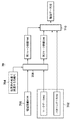
図1は、本発明の一側面としての描画装置1の構成を示す図である。描画装置1は、荷電粒子線(電子線)を用いて基板にパターンを描画するリソグラフィ装置である。描画装置1は、本実施形態では、マルチビーム型の描画装置として構成されているが、シングルビーム型の描画装置として構成されていてもよい。
FIG. 1 is a diagram showing a configuration of a
描画装置1は、複数の電子源10a、10b及び10cと、荷電粒子光学系20と、偏向器30と、ダイナミックフォーカスコイル40と、ダイナミックスティグコイル50と、基板ステージ60と、描画データ生成部70と、制御部80とを有する。
The
電子源10a、10b及び10cのそれぞれは、例えば、電子銃を含み、荷電粒子線(電子線)の照射(ON)及び非照射(OFF)が個別に制御される。荷電粒子光学系20は、電子源10a、10b及び10cのそれぞれからの荷電粒子線を基板STに導く光学系である。偏向器30は、荷電粒子光学系20によって基板STに導かれる荷電粒子線を偏向(走査)する。ダイナミックフォーカスコイル40は、偏向器30を動作させた際に、荷電粒子光学系20を通過する荷電粒子線に発生する偏向収差に応じて、荷電粒子線のフォーカス位置を補正する。ダイナミックスティグコイル50は、荷電粒子光学系20を通過する荷電粒子線に発生する偏向収差に応じて、荷電粒子線の非点収差を補正する。基板ステージ60は、基板STを保持して移動する。
Each of the
描画装置1において、電子源10a、10b及び10c、荷電粒子光学系20、偏向器30、ダイナミックフォーカスコイル40、ダイナミックスティグコイル50及び基板ステージ60は、描画処理部を構成する。かかる描画処理部は、制御部80の制御下で、描画処理を行う。
In the
描画データ生成部70は、CADデータやベクトルデータをビットマップデータに変換する機能などを有し、基板STに描画すべきパターンに対応する描画データを生成する。描画データ生成部70については、後で詳細に説明する。
The drawing
制御部80は、CPUやメモリなどを含み、描画装置1の全体(動作)を制御する。例えば、制御部80は、描画データ生成部70で生成された描画データに基づいて描画処理部(を構成する各部)を制御して、荷電粒子線を基板STの上で走査させることで基板STにパターンを描画させる。
The
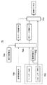
ここで、図2を参照して、描画データ生成部70による描画データの生成の概要について説明する。図2は、描画データ生成部70の基本的な構成を示す図である。描画データ生成部70は、記憶部702と、取得部704と、保持部706と、決定部708と、生成部710とを含む。
Here, an outline of generation of drawing data by the drawing
記憶部702は、CADデータやベクトルデータである設計データを記憶する。上述したように、従来技術では、設計データは、基板に描画すべき回路パターンを表すパターンデータ及び基板を計測又は検査するために基板に描画すべきマーク(アライメントマークや検査マーク)を表すマークデータを含んでいる。換言すれば、従来技術では、回路パターンとマークデータとを区別することなく、1つの設計データとして記憶していた。一方、本実施形態では、記憶部702は、基板STに描画すべき回路パターンを表すパターンデータPDと、基板STに描画すべきマークを表すマークデータMDとをそれぞれ別のデータとして記憶する。但し、マークデータMDのうち、描画位置精度に厳しくなく、装置状況に応じて柔軟に描画領域(描画位置)を変更する必要がないマークや描画領域を固定したいマークを表すマークデータは、パターンデータPDの一部としてもよい。
The
取得部704は、基板STに対する荷電粒子線の位置決め精度に関連する情報PIを取得する。ここで、情報PIは、例えば、基板STの各位置での平面度を表す面形状情報(平面度情報)SI、描画装置1のキャリブレーションの実行時刻を表す時刻情報TI、描画装置1の環境を表す環境情報EIなどの少なくとも1つを含む。
The
保持部706は、基板STにおいてマーク(アライメントマークや検査マークなど)を描画可能な領域を表す領域情報MDRを保持する。ここで、マークを描画可能な領域とは、その領域内であれば自由にマークを描画することが可能である領域である。また、領域情報MDRは、ユーザが任意に設定してもよいし、描画装置1が基板STに描画すべき回路パターン(パターンデータPD)から自動的に設定してもよい。
The holding
決定部708は、取得部704で取得された情報PIに基づいて、保持部706で保持した領域情報MDRが表す領域の中から、基板STに描画される回路パターンに対するマークの描画領域を決定する。換言すれば、決定部708は、情報PI及び領域情報MDRを解析することで、基板STにおけるマークの最適な描画領域(描画タイミング)やマークの形状及び寸法を決定する。また、決定部708は、決定したマークの描画領域を表す第1マーク情報FMIと、決定したマークの形状及び寸法を表す第2マーク情報SMIとを生成して生成部710に入力する。なお、決定部708は、取得部704で取得された情報PIに基づいて、保持部706で保持した領域情報MDRに関わらず、マークの描画領域を任意に決定することも可能である。
Based on the information PI acquired by the
生成部710は、決定部708で決定した描画領域にマークが描画されるように、記憶部702に記憶したパターンデータPDとマークデータMDとを合成して描画データDDを生成する。具体的には、生成部710は、第1マーク情報FMI及び第2マーク情報SMIに基づいて、パターンデータPDとマークデータMDとを合成した合成データを生成し、かかる合成データをビットマップデータに変換することで描画データDDを生成する。
The
描画装置1において、描画領域(描画位置)と描画タイミングとは一体的なものであって、描画領域が決定されれば描画タイミングも決定され、描画タイミングが決定されれば描画領域も決定される。従って、描画領域の要請から描画タイミングが決定される場合と、描画タイミングの要請から描画領域が決定される場合とがある。
In the
また、描画装置1では、描画を開始する前にある程度の量(例えば、1チップ分)のパターンデータとマークデータとを合成して描画データを生成する場合と、描画順にパターンデータとマークデータとを合成して描画データを順次生成する場合とがある。以下で説明する各実施形態は、どちらの場合にも対応可能であるが、第2の実施形態(描画タイミングの要請から描画領域が決定される場合)では、描画順にパターンデータとマークデータとを合成して描画データを順次生成する場合を想定している。但し、第2の実施形態であっても、条件次第では、描画を開始する前にある程度の量のパターンデータとマークデータとを合成して描画データを生成することも可能である。
In the
以下、各実施形態において、描画データ生成部70について具体的に説明する。
Hereinafter, in each embodiment, the drawing
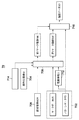
<第1の実施形態>
図3は、第1の実施形態における描画データ生成部70の構成を示す図である。基板STの上の領域のうち、ゴミが付着している領域や面形状が荒れている領域にアライメントマークや検査マークなどのマークを描画することは、アライメント精度や検査精度を低下させる要因となる。従って、このような領域にマークを描画することを回避する必要がある。
<First Embodiment>
FIG. 3 is a diagram illustrating a configuration of the drawing
そこで、本実施形態では、取得部704は、基板STに対する荷電粒子線の位置決め精度に関連する情報PIとして、基板STの各位置での平面度を表す面形状情報SIを取得する。基板STの上のゴミが付着している領域や面形状が荒れている領域などは、基板面内のフォーカス偏差を検査する工程において、フォーカス位置がその他の領域と大きく異なる。従って、面形状情報SIは、基板面内のフォーカス偏差から取得することが可能である。
Therefore, in the present embodiment, the
決定部708は、面形状情報SIに基づいて、保持部706で保持した領域情報MDRが表す領域のうち、平面度が許容範囲内にある領域(必要な平面度を満たす領域)、例えば、ゴミが付着していない領域からマークの描画領域を決定する。但し、領域情報MDRが表す領域に必要な平面度を満たす領域が十分に存在していない場合には、決定部708は、マークの形状及び寸法を変更することが可能である。換言すれば、決定部708は、必要な平面度を満たす領域にマークが描画されるように、マークの形状及び寸法を決定することが可能である。一般的に、マークの形状と寸法とは一体的に決定されるものであり、マークの寸法を変更すれば、それに伴ってマークの形状も変更される。
Based on the surface shape information SI, the
領域情報MDRが表す領域に必要な平面度を満たす領域が存在しない場合には、決定部708は、その旨を通知するためのエラー(又は警告)メッセージを描画装置1の表示部(不図示)に表示したり、制御部80のメモリなどにエラーログを記録したりする。また、領域情報MDRが表す領域に必要な平面度を満たす領域が存在しない場合には、決定部708は、領域情報MDRや面形状情報SIに関わらず、デフォルトで指定されている描画領域をマークの描画領域として決定してもよい。
If there is no area satisfying the required flatness in the area represented by the area information MDR, the
本実施形態によれば、基板STの平面度に応じて、アライメントマークや検査マークなどのマークを描画する描画領域を決定(変更)することができるため、アライメント精度や検査精度の低下を低減(防止)することが可能となる。また、本実施形態では、マルチビーム型の描画装置であってもシングルビーム型の描画装置であっても、マークの描画領域が決定されれば、マークの描画位置に応じて描画タイミングは一意に決定される。 According to the present embodiment, a drawing region for drawing marks such as alignment marks and inspection marks can be determined (changed) in accordance with the flatness of the substrate ST, thereby reducing a decrease in alignment accuracy and inspection accuracy ( Prevention). In this embodiment, even if the drawing apparatus is a multi-beam type drawing apparatus or a single beam type drawing apparatus, if the drawing area of the mark is determined, the drawing timing is uniquely determined according to the drawing position of the mark. It is determined.
<第2の実施形態>
図4は、第2の実施形態における描画データ生成部70の構成を示す図である。本実施形態では、描画装置1の状態をリアルタイムで監視し、かかる描画装置1の状態に応じて割り込みをかけてアライメントマークや検査マークなどのマークを描画する。従って、パターンデータPDは描画順に読み出され、或いは、微小領域に分割され、割り込みがかかった際に、パターンデータPDとマークデータMDとを合成して描画データDDを生成する。
<Second Embodiment>
FIG. 4 is a diagram illustrating a configuration of the drawing
そこで、本実施形態では、取得部704は、描画装置1のキャリブレーションの実行時刻を表す時刻情報TIや描画装置1の環境を表す環境情報EIを取得する。決定部708は、取得部704で取得した時刻情報TIや環境情報EIに基づいて、マークを描画する描画条件を満たすときに、マーク描画フラグをたててマークの描画領域を決定する。ここで、環境情報EIは、例えば、基板STの温度を表す温度情報を含む。
Therefore, in the present embodiment, the
取得部704が環境情報EIを取得する場合、決定部708は、基板STの温度が所定の温度に到達したタイミングでマークが描画されるように、マークの描画領域(描画タイミング)を決定する。換言すれば、決定部708は、環境情報EIに基づいて、描画装置1の環境が許容範囲内にあるタイミングでマークが描画されるように、保持部706で保持した領域情報MDRが表す領域からマークの描画領域を決定する。これにより、基板STの温度変化に影響されることなく、基板STに描画することが可能となる。
When the
また、取得部704が時刻情報TIを取得する場合、決定部708は、描画装置1のキャリブレーションが行われた直後のタイミングでマークが描画されるように、マークの描画領域(描画タイミング)を決定する。換言すれば、決定部708は、時刻情報TIに基づいて、描画装置1のキャリブレーションの実行時刻後の予め定められた期間内にマークが描画されるように、保持部706で保持した領域情報MDRが表す領域からマークの描画領域を決定する。
When the
描画装置1においては、実際には、回路パターンやマークを描画する描画タイミングは予め検知することが可能であり、回路パターンやマークを描画する前に十分な余裕をもって描画データを生成することが可能な場合もある。例えば、描画装置1のキャリブレーションのスケジュールが決まっている場合などには、1チップ分のパターンデータPDとマークデータMDとを合成して描画データDDを生成してから描画を開始することも可能である。
In the
また、本実施形態では、環境情報EIや時刻情報TIに応じてマークの描画タイミングが一意に決定されているが、マークの描画ごとやマークの種類ごとに描画タイミングを変更してもよい。 In this embodiment, the mark drawing timing is uniquely determined according to the environment information EI and the time information TI. However, the drawing timing may be changed for each mark drawing or each mark type.
マルチビーム型の描画装置の場合、描画範囲が大画角であるため、回路パターンとマークとを同時に描画することが可能である。従って、回路パターンを描画するタイミングと同じタイミングでマークが描画されるように、マークの描画領域(描画タイミング)を決定することができる。具体的には、マーク描画フラグをたてたとき又はそれにできるだけ近いときに、マークが描画されるように、マークを描画可能な領域からマークの描画領域を決定する。 In the case of a multi-beam type drawing apparatus, since the drawing range has a large angle of view, it is possible to draw a circuit pattern and a mark simultaneously. Therefore, the mark drawing area (drawing timing) can be determined so that the mark is drawn at the same timing as the circuit pattern drawing timing. Specifically, the mark drawing area is determined from the area where the mark can be drawn so that the mark is drawn when the mark drawing flag is set or as close as possible.
一方、シングルビーム型の描画装置の場合、回路パターンとマークとを同時に描画することが不可能である。従って、マーク描画フラグをたててからできるだけ近いときに、マークが描画されるように、マークを描画可能な領域からマークの描画領域を決定する。但し、シングルビーム型の描画装置の場合、マークを描画する際に基板ステージ60を移動させなければならないこともあるため、マルチビーム型の描画装置と比較して、マークの描画精度が低下する可能性がある。
On the other hand, in the case of a single beam type drawing apparatus, it is impossible to draw a circuit pattern and a mark simultaneously. Accordingly, the mark drawing area is determined from the area where the mark can be drawn so that the mark is drawn as close as possible after the mark drawing flag is set. However, in the case of a single-beam type drawing apparatus, the
また、取得部704は、環境情報EIや時刻情報TIに加えて、面形状情報SIを取得することも可能である。この場合、マークの描画領域を決定する前に、面形状情報SIに基づいて、保持部706で保持した領域情報MDRが表す領域から平面度が許容範囲外である領域を除外しておいてもよい。このように、保持部706で保持した領域情報MDRを更新することによって、環境情報EIや時刻情報TIに基づいたマークの描画領域の決定を効率的に行うことができる。
The
また、第1の実施形態と同様に、保持部706で保持した領域情報MDRが表す領域に必要な平面度を満たす領域が十分に存在していない場合には、決定部708は、マークの形状及び寸法を変更することが可能である。
Similarly to the first embodiment, when there is not a sufficient area satisfying the required flatness in the area represented by the area information MDR held by the holding
更に、領域情報MDRが表す領域に必要な平面度を満たす領域が存在しない場合には、決定部708は、その旨を通知するためのエラー(又は警告)メッセージを描画装置1の表示部(不図示)に表示したり、制御部80のメモリなどにエラーログを記録したりする。また、領域情報MDRが表す領域に必要な平面度を満たす領域が存在しない場合には、決定部708は、環境情報EI、時刻情報TIに関わらず、デフォルトで指定されている描画領域をマークの描画領域として決定してもよい。
Further, when there is no region that satisfies the required flatness in the region represented by the region information MDR, the
本実施形態によれば、描画装置1の装置状態に応じて、アライメントマークや検査マークなどのマークを描画する描画領域を決定(変更)することができるため、アライメント精度や検査精度の低下を低減(防止)することが可能となる。
According to the present embodiment, the drawing area for drawing marks such as alignment marks and inspection marks can be determined (changed) in accordance with the apparatus state of the
<第3の実施形態>
図5は、第3の実施形態における描画データ生成部70の構成を示す図である。荷電粒子線で基板STに描画を行う描画装置1は、露光装置と比較して、パターンの描画に時間がかかるため、パターンの描画中にアライメント精度が低下することがある。従って、本実施形態では、重要な回路パターン(クリティカルパターン)の描画タイミングとアライメントマークなどのマークの描画タイミングとを合わせることで、描画タイミングのずれに起因するアライメント精度の低下を低減(防止)する。
<Third Embodiment>
FIG. 5 is a diagram illustrating a configuration of the drawing
そこで、本実施形態では、描画データ生成部70は、記憶部702に記憶したパターンデータPDを解析して、回路パターンを構成するパターン要素の密度(集積度)を表す密度情報DIを算出する算出部712を含む。換言すれば、算出部712は、密度情報DIを取得する取得部として機能する。また、決定部708は、算出部712で算出された密度情報DIに基づいて、密度が予め定められた値以上となるパターン要素(パターン要素群)、即ち、クリティカルパターンを特定する。そして、決定部708は、特定したクリティカルパターンの描画と並行してマークが描画されるように、保持部706で保持した領域情報MDRが表す領域からマークの描画領域を決定する。
Therefore, in the present embodiment, the drawing
このように、本実施形態では、クリティカルパターンの描画タイミングに応じてマークの描画領域(描画タイミング)を決定する。但し、基板STの上の複数のチップ領域(ショット領域)の全てに同じ回路パターンが描画される場合には、チップ領域の全てに対してマークを描画する必要はない。また、基板STのチップ領域ごとに、マークの描画領域(描画タイミング)を変更してもよい。 Thus, in the present embodiment, the mark drawing area (drawing timing) is determined according to the drawing timing of the critical pattern. However, when the same circuit pattern is drawn on all of the plurality of chip areas (shot areas) on the substrate ST, it is not necessary to draw marks on all of the chip areas. Further, the mark drawing area (drawing timing) may be changed for each chip area of the substrate ST.
マルチビーム型の描画装置の場合、上述したように、描画範囲が大画角であるため、回路パターンとマークとを同時に描画することが可能である。従って、クリティカルパターンの描画と並行してマークが描画されるように、マークの描画領域(描画タイミング)を決定することができる。具体的には、クリティカルパターンを描画するタイミング又はそれにできるだけ近いタイミングでマークが描画されるように、マークを描画可能な領域からマークの描画領域を決定する。 In the case of a multi-beam type drawing apparatus, as described above, since the drawing range has a large angle of view, a circuit pattern and a mark can be drawn simultaneously. Therefore, the mark drawing area (drawing timing) can be determined so that the mark is drawn in parallel with the drawing of the critical pattern. Specifically, the drawing area of the mark is determined from the area where the mark can be drawn so that the mark is drawn at the timing when the critical pattern is drawn or at the timing as close as possible.
一方、シングルビーム型の描画装置の場合、回路パターンとマークとを同時に描画することが不可能である。従って、クリティカルパターンを描画するタイミングからできるだけ近いタイミングでマークが描画されるように、マークを描画可能な領域からマークの描画領域を決定する。但し、シングルビーム型の描画装置の場合、マークを描画する際に基板ステージ60を移動させなければならないこともあるため、マルチビーム型の描画装置と比較して、マークの描画精度が低下する可能性がある。
On the other hand, in the case of a single beam type drawing apparatus, it is impossible to draw a circuit pattern and a mark simultaneously. Accordingly, the mark drawing area is determined from the area where the mark can be drawn so that the mark is drawn as close as possible to the timing of drawing the critical pattern. However, in the case of a single-beam type drawing apparatus, the
また、取得部704が面形状情報SIを取得している場合には、マークの描画領域を決定する前に、面形状情報SIに基づいて、保持部706で保持した領域情報MDRが表す領域から平面度が許容範囲外である領域を除外しておいてもよい。このように、保持部706で保持した領域情報MDRを更新することによって、密度情報DIに基づいたマークの描画領域の決定を効率的に行うことができる。
Further, when the
また、第1の実施形態と同様に、保持部706で保持した領域情報MDRが表す領域に必要な平面度を満たす領域が十分に存在していない場合には、決定部708は、マークの形状及び寸法を変更することが可能である。
Similarly to the first embodiment, when there is not a sufficient area satisfying the required flatness in the area represented by the area information MDR held by the holding
更に、領域情報MDRが表す領域に必要な平面度を満たす領域が存在しない場合には、決定部708は、その旨を通知するためのエラー(又は警告)メッセージを描画装置1の表示部(不図示)に表示したり、制御部80のメモリなどにエラーログを記録したりする。また、領域情報MDRが表す領域に必要な平面度を満たす領域が存在しない場合には、決定部708は、密度情報DIに関わらず、デフォルトで指定されている描画領域をマークの描画領域として決定してもよい。
Further, when there is no region that satisfies the required flatness in the region represented by the region information MDR, the
本実施形態によれば、基板STに描画する回路パターンを構成するパターン要素(例えば、クリティカルパターン)に応じて、アライメントマークなどのマークを描画する描画領域を決定(変更)することができる。従って、クリティカルパターンの描画タイミングとアライメントマークなどのマークの描画タイミングとを合わせることが可能となり、描画タイミングのずれに起因するアライメント精度の低下を低減(防止)することができる。 According to the present embodiment, it is possible to determine (change) a drawing area for drawing a mark such as an alignment mark in accordance with a pattern element (for example, a critical pattern) constituting a circuit pattern to be drawn on the substrate ST. Therefore, it becomes possible to match the drawing timing of the critical pattern with the drawing timing of the mark such as the alignment mark, and it is possible to reduce (prevent) the deterioration of the alignment accuracy due to the deviation of the drawing timing.
<第4の実施形態>
図6は、第4の実施形態における描画データ生成部70の構成を示す図である。第3の実施形態では、算出部712で算出された密度情報DIに基づいて、決定部708がクリティカルパターンを自動的に特定している。本実施形態では、回路パターンを構成するパターン要素のうち、着目するパターン要素(例えば、クリティカルパターン)をユーザが任意に指定できるようにする。
<Fourth Embodiment>
FIG. 6 is a diagram illustrating a configuration of the drawing
そこで、本実施形態では、描画データ生成部70は、記憶部702に記憶したパターンデータPDから回路パターンを構成するパターン要素を選択する選択部714を含む。選択部714は、ユーザの指定に応じて、回路パターンを構成するパターン要素から着目するパターン要素を選択する。そして、決定部708は、選択部714で選択されたパターン要素の描画と並行してマークが描画されるように、保持部706で保持した領域情報MDRが表す領域からマークの描画領域を決定する。なお、描画データ生成部70が算出部712を含む場合には、算出部712で算出された密度情報DIをユーザに提供し、ユーザは密度情報DIを参照しながら着目するパターン要素を指定することも可能である。
Therefore, in the present embodiment, the drawing
このように、本実施形態では、選択部714で選択されたパターン要素の描画タイミングに応じてマークの描画領域(描画タイミング)を決定する。但し、基板STの上の複数のチップ領域(ショット領域)の全てに同じ回路パターンが描画される場合には、チップ領域の全てに対してマークを描画する必要はない。また、基板STのチップ領域ごとに、マークの描画領域(描画タイミング)を変更してもよい。
As described above, in this embodiment, the mark drawing area (drawing timing) is determined according to the drawing timing of the pattern element selected by the
マルチビーム型の描画装置の場合、上述したように、描画範囲が大画角であるため、回路パターンとマークとを同時に描画することが可能である。従って、選択部714で選択されたパターン要素の描画と並行してマークが描画されるように、マークの描画領域(描画タイミング)を決定することができる。具体的には、選択部714で選択されたパターン要素を描画するタイミング又はそれにできるだけ近いタイミングでマークが描画されるように、マークを描画可能な領域からマークの描画領域を決定する。
In the case of a multi-beam type drawing apparatus, as described above, since the drawing range has a large angle of view, a circuit pattern and a mark can be drawn simultaneously. Therefore, the mark drawing area (drawing timing) can be determined so that the mark is drawn in parallel with the drawing of the pattern element selected by the
一方、シングルビーム型の描画装置の場合、回路パターンとマークとを同時に描画することが不可能である。従って、選択部714で選択されたパターン要素を描画するタイミングからできるだけ近いタイミングでマークが描画されるように、マークを描画可能な領域からマークの描画領域を決定する。但し、シングルビーム型の描画装置の場合、マークを描画する際に基板ステージ60を移動させなければならないこともあるため、マルチビーム型の描画装置と比較して、マークの描画精度が低下する可能性がある。
On the other hand, in the case of a single beam type drawing apparatus, it is impossible to draw a circuit pattern and a mark simultaneously. Accordingly, the drawing area of the mark is determined from the area where the mark can be drawn so that the mark is drawn as close as possible to the timing of drawing the pattern element selected by the
また、取得部704が面形状情報SIを取得している場合には、マークの描画領域を決定する前に、面形状情報SIに基づいて、保持部706で保持した領域情報MDRが表す領域から平面度が許容範囲外である領域を除外しておいてもよい。このように、保持部706で保持した領域情報MDRを更新することによって、選択部714で選択されたパターン要素の描画タイミングに基づいたマークの描画領域の決定を効率的に行うことができる。
Further, when the
また、第1の実施形態と同様に、保持部706で保持した領域情報MDRが表す領域に必要な平面度を満たす領域が十分に存在していない場合には、決定部708は、マークの形状及び寸法を変更することが可能である。
Similarly to the first embodiment, when there is not a sufficient area satisfying the required flatness in the area represented by the area information MDR held by the holding
更に、領域情報MDRが表す領域に必要な平面度を満たす領域が存在しない場合には、決定部708は、その旨を通知するためのエラー(又は警告)メッセージを描画装置1の表示部(不図示)に表示したり、制御部80のメモリなどにエラーログを記録したりする。また、領域情報MDRが表す領域に必要な平面度を満たす領域が存在しない場合には、決定部708は、選択部714で選択されたパターン要素の描画タイミングに関わらず、デフォルトで指定されている描画領域をマークの描画領域として決定してもよい。
Further, when there is no region that satisfies the required flatness in the region represented by the region information MDR, the
本実施形態によれば、基板STに描画する回路パターンを構成するパターン要素から選択されたパターン要素(例えば、クリティカルパターン)に応じて、アライメントマークなどのマークを描画する描画領域を決定(変更)することができる。従って、選択されたパターン要素の描画タイミングとアライメントマークなどのマークの描画タイミングとを合わせることが可能となり、描画タイミングのずれに起因するアライメント精度の低下を低減(防止)することができる。 According to the present embodiment, a drawing area for drawing a mark such as an alignment mark is determined (changed) in accordance with a pattern element (for example, a critical pattern) selected from pattern elements constituting a circuit pattern to be drawn on the substrate ST. can do. Therefore, it is possible to match the drawing timing of the selected pattern element with the drawing timing of a mark such as an alignment mark, and it is possible to reduce (prevent) a decrease in alignment accuracy due to a shift in drawing timing.
<第5の実施形態>
図7は、第5の実施形態における描画データ生成部70の構成を示す図である。本実施形態では、面形状情報SI、環境情報EI及び時刻情報TIに加えて、基板STに形成されている各層に描画されたマークの描画領域を表すマーク領域情報MMIに基づいて、その上に形成されるターゲット層のマークの描画領域を決定する。
<Fifth Embodiment>
FIG. 7 is a diagram illustrating a configuration of the drawing
そこで、本実施形態では、描画データ生成部70は、基板STの上に形成された層のそれぞれについて、マークの描画領域を表すマーク領域情報MMIを管理する管理部716を含む。そして、決定部708は、ターゲット層について、管理部716で管理されたマーク領域情報MMIに基づいて、領域情報MDRが表す領域のうちターゲット層の下の層に描画されたマークと重ならない領域をマークの描画領域として決定する。これにより、ターゲット層に描画されたマークとターゲット層の下の層に描画されたマークとが重なってしまうことを防止することが可能となる。また、管理部716は、基板STに形成される層にマークが描画されるたびに、かかるマークが描画された領域をマーク領域情報MMIに反映させる。なお、管理部716は、基板STの上に形成されている層に描画されたマークの描画領域だけではなく、基板STの上にこれから形成される層に描画されるマークの描画領域もマーク領域情報MMIとして管理する。
Therefore, in the present embodiment, the drawing
管理部716で管理されるマーク領域情報MMIは、例えば、基板STの平面度の計測結果(面形状情報SI)をトリガーとして更新(変更)される。図8を参照して、管理部716で管理されるマーク領域情報MMIが更新される際の決定部708の処理について説明する。図8では、面形状情報SIをトリガーとしてマーク領域情報MMIが更新される場合を例として説明する。但し、描画装置1の環境(例えば、温度)の変化やキャリブレーションによる荷電粒子線のビームシフトの発生をトリガーとしてマーク領域情報MMIを更新してもよい。
The mark area information MMI managed by the management unit 716 is updated (changed) using, for example, a measurement result (surface shape information SI) of the flatness of the substrate ST as a trigger. With reference to FIG. 8, the process of the
S802において、取得部704は、基板STの各位置での平面度を表す面形状情報SIを取得する。S804において、決定部708は、管理部716で管理されたマーク領域情報MMIを参照して、ターゲット層であるn番目の層に描画されるマークの描画領域を特定する。
In step S802, the
S806において、決定部708は、取得部704で取得された面形状情報SI(S802)に基づいて、S804で特定されたマークの描画領域が必要な平面度を満たす領域であるかどうかを判定する。S804で特定されたマークの描画領域が必要な平面度を満たす領域である場合には、管理部716で管理されているマーク領域情報MMIを更新することなく、処理を終了する。一方、S804で特定されたマークの描画領域が必要な平面度を満たす領域でない場合には、S808に移行する。
In step S <b> 806, the
S808において、決定部708は、取得部704で取得された面形状情報SI(S802)に基づいて、保持部706で保持した領域情報MDRが表す領域から必要な平面度を満たす領域を抽出する。S810において、決定部708は、S808で抽出した領域を、n番目の層に描画されるマークの描画領域として仮決定する。S812において、決定部708は、S810で仮決定されたマークの描画領域、即ち、n番目の層に描画されるマークの描画領域として仮決定された領域を管理部716に通知する。
In step S <b> 808, the
S814において、決定部708は、管理部716で管理されたマーク領域情報MMIを参照して、n番目の層の下の層、即ち、1〜n−1番目の層に描画されているマークの描画領域を抽出する。S816において、決定部708は、S810で仮決定されたマークの描画領域から、S814で抽出されたマークの描画領域を除外して、n番目の層に対してマークを描画可能な複数の領域(マーク描画可能領域群)を定義する。
In step S814, the
S818において、決定部708は、S816で定義されたマーク描画可能領域群から1つの領域(任意の領域)を選択し、n番目の層に描画されるマークの描画領域として決定する。S820において、決定部708は、S818と同様に、n番目の層の上に形成されるn+1〜m番目の層のそれぞれに描画されるマークの描画領域を決定する。また、決定部708は、S818でn番目の層に描画されるマークの描画領域として決定された領域、及び、S820でn+1〜m番目の層のそれぞれに描画されるマークの描画領域として決定された領域を管理部716に通知する。そして、管理部716は、決定部708からの通知が反映されるように、マーク領域情報MMIを更新する。
In S818, the determining
S820において、決定部708は、管理部716で管理されたマーク領域情報MMIを参照して、n+1〜m番目の層のそれぞれに描画されるマークの描画領域が互いに重なっていないかどうかを判定する。n+1〜m番目の層のそれぞれに描画されるマークの描画領域が互いに重なっていない場合には、処理を終了する。一方、n+1〜m番目の層のそれぞれに描画されるマークの描画領域が互いに重なっている場合には、S818に移行し、マーク描画可能領域群から新たな領域を選択し、n番目の層に描画されるマークの描画領域として決定する。
In step S820, the
なお、S818及びS820を繰り返してもn〜m番目の層のそれぞれに描画されるマークの描画領域を決定できない場合や基板STの上の各層に必要な平面度を満たす領域が存在しない場合もある。このような場合には、その旨を通知するためのエラー(又は警告)メッセージを描画装置1の表示部(不図示)に表示したり、制御部80のメモリなどにエラーログを記録したりする。また、このような場合には、デフォルトで指定されている描画領域をマークの描画領域として決定する。
It should be noted that even if S818 and S820 are repeated, the drawing area of the mark drawn on each of the n to m-th layers cannot be determined, or there may be no area that satisfies the required flatness on each layer on the substrate ST. . In such a case, an error (or warning) message for notifying the fact is displayed on the display unit (not shown) of the
また、本実施形態では、基板STの上の下層(基板側の層)から上層の順序でマークの描画領域を決定しているが、マークの描画領域を決定する層の順序を限定するものではない。例えば、マークの描画領域を優先して決定したい層があることも考えられるため、マークの描画領域を決定する優先順位を各層に設定し、かかる優先順位に応じてマークの描画領域を決定してもよい。 In this embodiment, the mark drawing area is determined in the order of the upper layer from the lower layer on the substrate ST (layer on the substrate side). However, the order of the layers for determining the mark drawing area is not limited. Absent. For example, there may be a layer that gives priority to the mark drawing area. Therefore, the priority order for determining the mark drawing area is set for each layer, and the mark drawing area is determined according to the priority order. Also good.
図9は、管理部716で管理されるマーク領域情報MMIの一例を示す図である。マーク領域情報MMIは、基板STの上の各層のマーク情報を含み、それらのマーク情報は、互いに関連付けられている。従って、各層に描画されるマークの描画領域やマークの形状などが変更されても、マーク領域情報MMIを参照することで、後工程(例えば、アライメント工程や検査工程など)を問題なく行うことができる。なお、図9では、n番目の層のマーク情報とn+m番目の層のマーク情報とが示されている。 FIG. 9 is a diagram illustrating an example of the mark area information MMI managed by the management unit 716. The mark area information MMI includes mark information of each layer on the substrate ST, and the mark information is associated with each other. Therefore, even if the drawing area of the mark drawn on each layer, the shape of the mark, or the like is changed, the post process (for example, the alignment process or the inspection process) can be performed without any problem by referring to the mark area information MMI. it can. In FIG. 9, the mark information of the nth layer and the mark information of the n + mth layer are shown.
図9を参照するに、n番目の層のマーク情報には、アライメントマークの描画可能領域、検査マークの描画可能領域、n層の描画の際にアライメントに用いるアライメントマークの描画領域及び形状が含まれている。また、n番目の層のマーク情報には、n層の検査に用いる検査マークの描画領域及び形状、n層に描画されたアライメントマークの描画領域及び形状、n層に描画された検査マークの描画領域及び形状も含まれている。 Referring to FIG. 9, the mark information of the nth layer includes an alignment mark drawable area, an inspection mark drawable area, and an alignment mark draw area and shape used for alignment when drawing the n layer. It is. The mark information of the nth layer includes the drawing area and shape of the inspection mark used for the inspection of the n layer, the drawing area and shape of the alignment mark drawn on the n layer, and the drawing of the inspection mark drawn on the n layer. Regions and shapes are also included.
アライメントマークの描画領域は、アライメントマークの描画可能領域に含まれる領域から選択され、検査マークの描画領域は、検査マークの描画可能領域に含まれる領域から選択されている。また、n+m番目の層の位置合わせにn番目の層に描画されたアライメントマークを用いる場合には、n番目の層のマーク情報に含まれる、n番目の層に描画されたアライメントマークの描画領域及び形状を参照する。同様に、n+m番目の層の検査にn番目の層に描画された検査マークを用いる場合には、n番目の層のマーク情報に含まれる、n番目の層に描画された検査マークの描画領域及び形状を参照する。 The alignment mark drawing area is selected from the areas included in the alignment mark drawable area, and the inspection mark drawing area is selected from the areas included in the inspection mark drawable area. In addition, when an alignment mark drawn on the nth layer is used for alignment of the n + mth layer, a drawing area of the alignment mark drawn on the nth layer included in the mark information of the nth layer And refer to the shape. Similarly, when the inspection mark drawn on the nth layer is used for the inspection of the n + mth layer, the drawing area of the inspection mark drawn on the nth layer included in the mark information of the nth layer And refer to the shape.
本実施形態によれば、基板STの各層に描画されるアライメントマークや検査マークなどのマークが重ならないように(即ち、既に形成されたマークの描画領域と重ならないように)、新たなマークを描画する描画領域を決定(変更)することができる。 According to the present embodiment, new marks are added so that alignment marks and inspection marks drawn on each layer of the substrate ST do not overlap (that is, do not overlap the drawing area of already formed marks). The drawing area to be drawn can be determined (changed).
各実施形態で説明したように、描画装置1は、アライメント精度や検査精度の低下を低減(防止)することが可能であり、荷電粒子線と基板STとの位置合わせを高精度に行うことができる。従って、描画装置1は、高いスループットで経済性よく高品位な物品(半導体デバイス等のマイクロデバイスや微細構造を有する素子等)を提供することができる。本実施形態の物品の製造方法は、基板に塗布された感光剤に描画装置1を用いて潜像パターンを形成する工程(基板に描画を行う工程)と、かかる工程で潜像パターンが形成された基板を現像する工程とを含む。更に、かかる製造方法は、他の周知の工程(酸化、成膜、蒸着、ドーピング、平坦化、エッチング、レジスト剥離、ダイシング、ボンディング、パッケージング等)を含む。本実施形態の物品の製造方法は、従来の方法に比べて、物品の性能・品質・生産性・生産コストの少なくとも1つにおいて有利である。
As described in each embodiment, the
以上、本発明の好ましい実施形態について説明したが、本発明はこれらの実施形態に限定されないことはいうまでもなく、その要旨の範囲内で種々の変形及び変更が可能である。例えば、描画装置は、描画装置本体部、及び、かかる描画装置本体部とネットワークで接続するコンピュータシステムで構成されている。従って、描画装置本体部からの情報のフィードバックが不要である場合には、パターンデータとマークデータとを合成して描画データを生成する処理は、コンピュータシステムで行われてもよい。 As mentioned above, although preferable embodiment of this invention was described, it cannot be overemphasized that this invention is not limited to these embodiment, A various deformation | transformation and change are possible within the range of the summary. For example, the drawing apparatus includes a drawing apparatus main body and a computer system connected to the drawing apparatus main body via a network. Therefore, when feedback of information from the drawing apparatus main body is not required, the process of generating drawing data by combining pattern data and mark data may be performed by a computer system.
Claims (10)
前記基板に対する前記荷電粒子線の位置決め精度に関連する情報を取得する取得部と、
前記取得部で取得された情報に基づいて、前記マークの描画領域を決定する決定部と、
前記決定部で決定された描画領域に前記マークが描画されるように、前記パターンデータと前記マークデータとを合成して前記描画データを生成する生成部と、
を有することを特徴とする描画装置。 A drawing apparatus for drawing on a substrate with a charged particle beam based on drawing data generated from pattern data representing a circuit pattern to be drawn on the substrate and mark data representing a mark to be drawn on the substrate,
An acquisition unit for acquiring information related to positioning accuracy of the charged particle beam with respect to the substrate;
A determination unit that determines a drawing area of the mark based on the information acquired by the acquisition unit;
A generating unit that generates the drawing data by combining the pattern data and the mark data so that the mark is drawn in the drawing area determined by the determining unit;
A drawing apparatus comprising:
前記決定部は、前記保持部に保持された領域情報が表す領域の中から前記マークの描画領域を決定する、ことを特徴とする請求項1に記載の描画装置。 A holding unit for holding area information representing an area where the mark can be drawn on the substrate;
The drawing apparatus according to claim 1, wherein the determination unit determines the drawing region of the mark from the region represented by the region information held in the holding unit.
前記決定部は、前記平面度情報に基づいて、前記平面度が許容範囲内にある領域から前記マークの描画領域を決定する、ことを特徴とする請求項1又は2に記載の描画装置。 The acquisition unit acquires flatness information representing the flatness of the substrate as information related to the positioning accuracy,
The drawing apparatus according to claim 1, wherein the determination unit determines a drawing area of the mark from an area where the flatness is within an allowable range based on the flatness information.
前記決定部は、前記時刻情報に基づいて、前記キャリブレーションの実行時刻後の予め定められた期間内に前記マークが描画されるように、前記マークの描画領域を決定する、ことを特徴とする請求項1又は2に記載の描画装置。 The acquisition unit acquires time information indicating an execution time of calibration of the drawing apparatus as information related to the positioning accuracy,
The determination unit determines a drawing area of the mark based on the time information so that the mark is drawn within a predetermined period after the calibration execution time. The drawing apparatus according to claim 1 or 2.
前記決定部は、前記環境情報に基づいて、前記環境が許容範囲内にあるタイミングで前記マークが描画されるように、前記マークの描画領域を決定する、ことを特徴とする請求項1又は2に記載の描画装置。 The acquisition unit acquires environment information representing an environment of the drawing apparatus as information related to the positioning accuracy,
The said determination part determines the drawing area | region of the said mark so that the said mark may be drawn at the timing when the said environment is in a tolerance | permissible_range based on the said environment information. The drawing apparatus described in 1.
前記決定部は、前記密度情報に基づいて、前記密度が予め定められた値以上となるパターン要素群の描画と並行して前記マークが描画されるように、前記マークの描画領域を決定する、ことを特徴とする請求項1又は2に記載の描画装置。 The acquisition unit acquires density information representing the density of pattern elements constituting the circuit pattern as information related to the positioning accuracy,
The determination unit determines a drawing area of the mark based on the density information so that the mark is drawn in parallel with drawing of a pattern element group in which the density is equal to or higher than a predetermined value. The drawing apparatus according to claim 1 or 2, characterized in that
前記決定部は、前記選択部で選択されたパターン要素を描画と並行して前記マークが描画されるように、前記マークの描画領域を決定する、ことを特徴とする請求項1又は2に記載の描画装置。 A selection unit for selecting a pattern element constituting the circuit pattern from the pattern data;
The said determination part determines the drawing area | region of the said mark so that the said mark may be drawn in parallel with drawing the pattern element selected by the said selection part, The Claim 1 or 2 characterized by the above-mentioned. Drawing device.
前記決定部は、前記マーク領域情報に基づいて、既に形成されたマークの描画領域と重ならないように、新たなマークの描画領域を決定する、ことを特徴とする請求項1又は2に記載の描画装置。 For each of the layers formed on the substrate, it further includes a storage unit that stores mark area information representing a drawing area of the mark,
The said determination part determines the drawing area | region of a new mark so that it may not overlap with the drawing area | region of the mark already formed based on the said mark area | region information. Drawing device.
前記ステップで描画を行われた前記基板を現像するステップと、
を有することを特徴とする物品の製造方法。 Drawing on a substrate using the drawing apparatus according to any one of claims 1 to 9,
Developing the substrate on which the drawing has been performed in the step;
A method for producing an article comprising:
Priority Applications (2)
| Application Number | Priority Date | Filing Date | Title |
|---|---|---|---|
| JP2011286620A JP2013135194A (en) | 2011-12-27 | 2011-12-27 | Drawing device and article manufacturing method |
| US13/705,754 US8779396B2 (en) | 2011-12-27 | 2012-12-05 | Drawing apparatus, and method of manufacturing article |
Applications Claiming Priority (1)
| Application Number | Priority Date | Filing Date | Title |
|---|---|---|---|
| JP2011286620A JP2013135194A (en) | 2011-12-27 | 2011-12-27 | Drawing device and article manufacturing method |
Publications (2)
| Publication Number | Publication Date |
|---|---|
| JP2013135194A true JP2013135194A (en) | 2013-07-08 |
| JP2013135194A5 JP2013135194A5 (en) | 2015-02-19 |
Family
ID=48654894
Family Applications (1)
| Application Number | Title | Priority Date | Filing Date |
|---|---|---|---|
| JP2011286620A Pending JP2013135194A (en) | 2011-12-27 | 2011-12-27 | Drawing device and article manufacturing method |
Country Status (2)
| Country | Link |
|---|---|
| US (1) | US8779396B2 (en) |
| JP (1) | JP2013135194A (en) |
Cited By (1)
| Publication number | Priority date | Publication date | Assignee | Title |
|---|---|---|---|---|
| JP2016122676A (en) * | 2014-12-24 | 2016-07-07 | 株式会社アドバンテスト | Exposure device and exposure method |
Families Citing this family (2)
| Publication number | Priority date | Publication date | Assignee | Title |
|---|---|---|---|---|
| JP5825291B2 (en) * | 2013-04-15 | 2015-12-02 | コニカミノルタ株式会社 | Image forming apparatus and reference image reading method |
| JP2016004881A (en) * | 2014-06-16 | 2016-01-12 | キヤノン株式会社 | Lithography apparatus, and method of manufacturing article |
Citations (8)
| Publication number | Priority date | Publication date | Assignee | Title |
|---|---|---|---|---|
| JPH05304080A (en) * | 1991-08-15 | 1993-11-16 | Jeol Ltd | Drawing method by charged particle beam |
| JPH07130624A (en) * | 1993-11-02 | 1995-05-19 | Fujitsu Ltd | Electron beam exposure |
| JP2002062636A (en) * | 1991-07-18 | 2002-02-28 | Dainippon Printing Co Ltd | Pattern forming method for patterned plate with alignment pattern and patterned plate pattern-formed by the method |
| JP2003086496A (en) * | 2001-09-13 | 2003-03-20 | Nikon Corp | Transfer mask and manufacturing method, and projection exposure method |
| JP2005072213A (en) * | 2003-08-22 | 2005-03-17 | Semiconductor Leading Edge Technologies Inc | Charged-particle beam exposure method |
| JP2008521221A (en) * | 2004-11-17 | 2008-06-19 | イーエムエス ナノファブリカツィオン アーゲー | Pattern lock device for particle beam exposure apparatus |
| WO2010110237A1 (en) * | 2009-03-26 | 2010-09-30 | Hoya株式会社 | Substrate provided with multilayer reflection film for reflective mask, reflective mask blank, and methods for manufacturing the substrate and the mask blank |
| JP2011198952A (en) * | 2010-03-18 | 2011-10-06 | Nuflare Technology Inc | Generating method of data for drawing charged particle beam and data generation device for drawing charged particle beam |
Family Cites Families (6)
| Publication number | Priority date | Publication date | Assignee | Title |
|---|---|---|---|---|
| EP0664033B1 (en) | 1992-11-02 | 2002-02-06 | Etec Systems, Inc. | Rasterizer for a pattern generation apparatus |
| JP4023262B2 (en) * | 2002-09-02 | 2007-12-19 | ソニー株式会社 | Alignment method, exposure method, exposure apparatus, and mask manufacturing method |
| US7462848B2 (en) * | 2003-10-07 | 2008-12-09 | Multibeam Systems, Inc. | Optics for generation of high current density patterned charged particle beams |
| US7868300B2 (en) * | 2005-09-15 | 2011-01-11 | Mapper Lithography Ip B.V. | Lithography system, sensor and measuring method |
| JP4855875B2 (en) * | 2006-09-06 | 2012-01-18 | 富士フイルム株式会社 | Electron beam drawing apparatus and electron beam deviation compensation method |
| JP5841710B2 (en) * | 2010-03-17 | 2016-01-13 | 株式会社ニューフレアテクノロジー | Charged particle beam drawing apparatus and charged particle beam drawing method |
-
2011
- 2011-12-27 JP JP2011286620A patent/JP2013135194A/en active Pending
-
2012
- 2012-12-05 US US13/705,754 patent/US8779396B2/en not_active Expired - Fee Related
Patent Citations (8)
| Publication number | Priority date | Publication date | Assignee | Title |
|---|---|---|---|---|
| JP2002062636A (en) * | 1991-07-18 | 2002-02-28 | Dainippon Printing Co Ltd | Pattern forming method for patterned plate with alignment pattern and patterned plate pattern-formed by the method |
| JPH05304080A (en) * | 1991-08-15 | 1993-11-16 | Jeol Ltd | Drawing method by charged particle beam |
| JPH07130624A (en) * | 1993-11-02 | 1995-05-19 | Fujitsu Ltd | Electron beam exposure |
| JP2003086496A (en) * | 2001-09-13 | 2003-03-20 | Nikon Corp | Transfer mask and manufacturing method, and projection exposure method |
| JP2005072213A (en) * | 2003-08-22 | 2005-03-17 | Semiconductor Leading Edge Technologies Inc | Charged-particle beam exposure method |
| JP2008521221A (en) * | 2004-11-17 | 2008-06-19 | イーエムエス ナノファブリカツィオン アーゲー | Pattern lock device for particle beam exposure apparatus |
| WO2010110237A1 (en) * | 2009-03-26 | 2010-09-30 | Hoya株式会社 | Substrate provided with multilayer reflection film for reflective mask, reflective mask blank, and methods for manufacturing the substrate and the mask blank |
| JP2011198952A (en) * | 2010-03-18 | 2011-10-06 | Nuflare Technology Inc | Generating method of data for drawing charged particle beam and data generation device for drawing charged particle beam |
Cited By (1)
| Publication number | Priority date | Publication date | Assignee | Title |
|---|---|---|---|---|
| JP2016122676A (en) * | 2014-12-24 | 2016-07-07 | 株式会社アドバンテスト | Exposure device and exposure method |
Also Published As
| Publication number | Publication date |
|---|---|
| US20130164692A1 (en) | 2013-06-27 |
| US8779396B2 (en) | 2014-07-15 |
Similar Documents
| Publication | Publication Date | Title |
|---|---|---|
| JP4593236B2 (en) | Dimensional measurement scanning electron microscope system, circuit pattern shape evaluation system and method | |
| US8867818B2 (en) | Method of creating template for matching, as well as device for creating template | |
| JP2018194847A (en) | Method of optimizing process window | |
| JP4846635B2 (en) | Pattern information generation method | |
| CN109863456A (en) | The method for determining the correction of patterning process | |
| JP5783953B2 (en) | Pattern evaluation apparatus and pattern evaluation method | |
| TW201602821A (en) | Computational wafer inspection | |
| US6757875B2 (en) | Method and apparatus of evaluating layer matching deviation based on CAD information | |
| JP5164598B2 (en) | Review method and review device | |
| JP2010067516A (en) | Method and device for synthesizing panorama image using scanning charged-particle microscope | |
| TW201131287A (en) | Selection of optimum patterns in a design layout based on diffraction signature analysis | |
| JP2007147366A (en) | Shape evaluation device for semiconductor pattern, and shape evaluation method of semiconductor pattern | |
| JP2012114202A (en) | Image pick-up device and image pick-up method | |
| US20050265592A1 (en) | Image data correction method, lithography simulation method, image data correction system, program , mask and method of manufacturing a semiconductor device | |
| KR20020082148A (en) | Pattern correction method of exposure mask, producing method of semiconductor device including pattern forming process and computer readable recording medium | |
| JP2022033027A (en) | Methods and systems for generating calibration data for wafer analysis | |
| JP2013135194A (en) | Drawing device and article manufacturing method | |
| US8144338B2 (en) | Pattern measurement apparatus and pattern measurement method | |
| TW201729003A (en) | Methods for identifying a process window boundary | |
| JP6399751B2 (en) | Mask pattern creation method, program, mask manufacturing method, exposure method, and article manufacturing method | |
| JP2017037194A (en) | Exposure device control method, exposure device, program, and article manufacturing method | |
| US10598617B2 (en) | Metrology guided inspection sample shaping of optical inspection results | |
| JP2015177032A (en) | Lithographic apparatus and method of manufacturing article | |
| JP2010050148A (en) | Method of measuring misalignment, and misalignment inspection mark | |
| JP2018022114A (en) | Measurement device, exposure device and method for producing article |
Legal Events
| Date | Code | Title | Description |
|---|---|---|---|
| A521 | Request for written amendment filed |
Free format text: JAPANESE INTERMEDIATE CODE: A523 Effective date: 20141226 |
|
| A621 | Written request for application examination |
Free format text: JAPANESE INTERMEDIATE CODE: A621 Effective date: 20141226 |
|
| A977 | Report on retrieval |
Free format text: JAPANESE INTERMEDIATE CODE: A971007 Effective date: 20151014 |
|
| A131 | Notification of reasons for refusal |
Free format text: JAPANESE INTERMEDIATE CODE: A131 Effective date: 20151019 |
|
| A02 | Decision of refusal |
Free format text: JAPANESE INTERMEDIATE CODE: A02 Effective date: 20160308 |