JP4761508B2 - Charged particle exposure apparatus and device manufacturing method - Google Patents
Charged particle exposure apparatus and device manufacturing method Download PDFInfo
- Publication number
- JP4761508B2 JP4761508B2 JP2005075830A JP2005075830A JP4761508B2 JP 4761508 B2 JP4761508 B2 JP 4761508B2 JP 2005075830 A JP2005075830 A JP 2005075830A JP 2005075830 A JP2005075830 A JP 2005075830A JP 4761508 B2 JP4761508 B2 JP 4761508B2
- Authority
- JP
- Japan
- Prior art keywords
- exposure
- charged particle
- sample
- exposure apparatus
- particle beam
- Prior art date
- Legal status (The legal status is an assumption and is not a legal conclusion. Google has not performed a legal analysis and makes no representation as to the accuracy of the status listed.)
- Expired - Fee Related
Links
Images


Landscapes
- Electron Beam Exposure (AREA)
Description
本発明は、主に半導体集積回路等の露光に用いられる電子ビーム露光装置、イオンビーム露光装置等の荷電粒子線露光装置に関し、特に、複数の荷電粒子線を用いてパターン描画を行うラスタースキャン型の荷電粒子線露光装置およびその荷電粒子線露光装置を用いるデバイス製造方法に関する。 The present invention relates to a charged particle beam exposure apparatus such as an electron beam exposure apparatus and an ion beam exposure apparatus mainly used for exposure of a semiconductor integrated circuit, and more particularly to a raster scan type that performs pattern drawing using a plurality of charged particle beams. The present invention relates to a charged particle beam exposure apparatus and a device manufacturing method using the charged particle beam exposure apparatus.
微小デバイス(ICやLSI等の半導体チップ、液晶パネル、CCD、薄膜磁気ヘッド、マイクロマシン等)を製造する際、試料上にパターンを形成するための従来の荷電粒子線露光装置は、荷電粒子源から放出される荷電粒子を加速、成形、縮小し、試料上にビーム照射することによって所望のパターンを試料上に形成している。ある形態の露光装置では上記ビームは一定面積を有し、所望の矩形、所望のパターン、もしくは所望の複数本ビームに成形され、試料に照射される。
以上の多くの形態の荷電粒子線露光装置では試料上のある部分の露光を行った後一旦ビーム照射を中止し、次に照射すべき試料上の位置を計算し、さらに補正を加え、偏向器に所望の電流もしくは電圧を印加し、更に前記電流もしくは電圧値が安定した後に再びビーム照射を行う。
一枚の試料の描画は以上の動作の繰り返しである。近年では荷電粒子線露光装置のスループット向上が望まれており、そのために上記サイクルを短縮するための工夫が各々なされている。試料へのビーム照射時間はビーム電流の増加、レジスト感度の向上等によって短縮が図られているが、試料にビームを露光しない時間の短縮については特にラスタースキャン型露光装置に関して最適化が図られていなかった。
また、特開2005−32888号公報(特許文献1)にて「荷電粒子線露光装置及び荷電粒子線露光方法」が提案され、露光装置の照明光学系中は、照明ビームをレチクルの各サブフィールドに向けて偏向する主偏向器と、照明ビームをレチクルに当てないようにブランキングするブランキング偏向器と、を有し、ブランキング偏向器を制御してブランキング時間を変えて、ウェハステージとレチクルステージの加減速中にも露光を行うことができるため、装置のスループットを向上できる。
In many of the charged particle beam exposure apparatuses described above, after a certain portion of the sample is exposed, the beam irradiation is temporarily stopped, the position on the sample to be irradiated next is calculated, further corrected, and the deflector A desired current or voltage is applied to the laser beam, and beam irradiation is performed again after the current or voltage value is stabilized.
Drawing of one sample is a repetition of the above operations. In recent years, it has been desired to improve the throughput of the charged particle beam exposure apparatus, and for that purpose, various measures have been taken to shorten the cycle. The beam irradiation time to the sample has been shortened by increasing the beam current and improving the resist sensitivity, etc., but the shortening of the time when the sample is not exposed to the beam has been optimized especially for the raster scan type exposure apparatus. There wasn't.
Japanese Patent Laying-Open No. 2005-32888 (Patent Document 1) proposes a “charged particle beam exposure apparatus and a charged particle beam exposure method”. In an illumination optical system of the exposure apparatus, an illumination beam is sent to each subfield of the reticle. A main deflector that deflects toward the reticle and a blanking deflector that blanks the illumination beam so as not to hit the reticle, and controls the blanking deflector to change the blanking time, and Since exposure can be performed even during acceleration / deceleration of the reticle stage, the throughput of the apparatus can be improved.
ラスタースキャン型露光装置ではビームをオンオフするクロックが一定であったため、荷電粒子線ビーム電流量の変化、レジスト感度の変化、更に近接効果補正による露光量変化に対して充分な考慮がなされていなかった。
すなわち露光量が変化してもクロックが一定であるため、荷電粒子線ビーム照射量が短縮されても荷電粒子線ビームの照射される時間と荷電粒子線ビームの照射されない時間の和は常に一定であり、描画時間が短縮されなかった。
そこで、本発明は、試料への荷電粒子線の照射されない時間を短縮することにより試料の描画時間を短縮し、スループットが向上するラスタースキャン型の荷電粒子露光装置およびその荷電粒子線露光装置を用いるデバイス製造方法を提供することを目的とする。
In the raster scan type exposure apparatus, since the clock for turning on and off the beam was constant, sufficient consideration was not given to changes in the charged particle beam current amount, changes in resist sensitivity, and changes in exposure amount due to proximity effect correction. .
In other words, since the clock is constant even when the exposure dose changes, the sum of the charged particle beam irradiation time and charged particle beam irradiation time is always constant even if the charged particle beam irradiation dose is shortened. Yes, the drawing time was not shortened.
Therefore, the present invention uses a raster scan type charged particle exposure apparatus and its charged particle beam exposure apparatus that reduce the drawing time of the sample by shortening the time during which the sample is not irradiated with the charged particle beam and improve the throughput. An object is to provide a device manufacturing method.
上記目的を達成するために本発明の荷電粒子線露光装置は、荷電粒子源からのビームをレジストが塗布された試料上に照射して露光を行う荷電粒子線露光装置であって、前記ビームを偏向し、前記ビームの前記試料上への照射を制御するブランキング手段と、前記ビームを偏向し、前記ビームを前記試料上で走査させる偏向器と、を備え、前記ブランキング手段および前記偏向器は、前記ビームが前記試料上に照射される時間と前記ビームが前記試料上に照射されない時間の和で表される露光サイクルで動作し、前記露光サイクルは、ビーム電流データ、レジスト感度データおよび近接効果補正データより前記ビームが前記試料上に照射される時間を求め、その結果に応じて前記ビームが前記試料上に照射されない時間を小さくするように、可変に設定されることを特徴とする。 The charged particle beam exposure device of the present invention in order to achieve the above object, a charged particle beam exposure apparatus for performing exposure by irradiating the beam onto the sample on which the resist is applied from a charged particle source, said beam deflect, and blanking means for controlling the irradiation onto the sample in the beam, to deflect the beam, and a deflector for scanning the beam over the sample, said blanking means and the deflector , the beam is operated with an exposure cycle time and the beam is irradiated is expressed by the sum of time that is not irradiated onto the sample on the sample, the exposure cycle, the beam current data, resist sensitivity data and proximity seek time the more effective correction data beam is irradiated onto the sample, such that said beam in response to the result to reduce the time that is not irradiated onto the sample, Characterized in that it is strange setting.
本発明の荷電粒子線露光装置によれば、1枚の前記試料を露光する時間内での試料への荷電粒子線の照射されない時間を小さくするように、ブランカーと偏向器を制御し露光サイクルを変化させるため、試料の描画時間を短縮し、スループットが向上する。
さらに、本発明のデバイス製造方法によれば、上記荷電粒子線露光装置を用いるため、試料の描画時間を短縮し、スループットが向上し、デバイス製造能率が向上する。
According to the charged particle beam exposure apparatus of the present invention, the exposure cycle is controlled by controlling the blanker and the deflector so as to reduce the time during which the sample is not irradiated with the charged particle beam within the time for exposing one sample. Since it is changed, the drawing time of the sample is shortened and the throughput is improved.
Furthermore, according to the device manufacturing method of the present invention, since the charged particle beam exposure apparatus is used, the drawing time of the sample is shortened, the throughput is improved, and the device manufacturing efficiency is improved.
以下、本発明を、その実施例に基づいて、図面を参照して説明する。 Hereinafter, the present invention will be described with reference to the drawings based on the embodiments.
以下、本発明の実施例1の荷電粒子線露光装置を説明する。
本発明の本実施例1のラスタースキャン型の荷電粒子線露光装置として、ラスタースキャン型マルチ電子ビーム露光装置が示される。
なお、電子ビームである荷電粒子線に限らずイオンビームを用いた露光装置にも同様に適用でき、マルチ電子ビームに限らずシングルビームについても同様の効果が得られる。
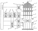
図1は本発明の実施例1の荷電粒子線露光装置の要部概略構成図である。
電子源1より放射状に放出される電子ビームである荷電粒子線10はコリメータレンズ2によって所望の大きさを持った面積ビームに成形された後、マスク3にほぼ垂直入射される。マスク3は複数のパターンを持つマスクである。マスク3を通して成形された荷電粒子線10はレンズアレイ4によって、各々ブランキングアレイ6に収束される。ブランキングアレイ6は偏向板アレイであり、ビームを個別に偏向することが出来る。ブランキングアレイ6によって偏向されたビームはブランキング絞り9によって遮蔽されるが、ブランキングアレイ6によって偏向されないビームはレンズ7,8によって縮小され、偏向器5によって試料11上の所望の位置に照射される。
一方、描画を行うための描画データはコントローラ12から描画パターン発生回路14に転送され、その後ビットマップ変換回路15によってビットマップに変換し、露光時間制御回路16によって個々のビームのブランキング時間が計算され、ブランキング制御回路17により制御信号が各々のブランキングアレイ6に印加される。また、レンズ2,4、7、8にはレンズ制御回路13から所望のレンズ電流及びレンズ電圧が、偏向器5には偏向信号発生回路18、偏向アンプ19によって計算された、試料11の所望の位置に荷電粒子線10を照射するべき偏向電圧が印加される。
The charged particle beam exposure apparatus according to the first embodiment of the present invention will be described below.
A raster scan type multi-electron beam exposure apparatus is shown as the raster scan type charged particle beam exposure apparatus of the first embodiment of the present invention.
Note that the present invention can be similarly applied to an exposure apparatus using an ion beam as well as a charged particle beam that is an electron beam, and the same effect can be obtained not only for a multi-electron beam but also for a single beam.
FIG. 1 is a schematic configuration diagram of a main part of a charged particle beam exposure apparatus according to a first embodiment of the present invention.
A
On the other hand, drawing data for drawing is transferred from the controller 12 to the drawing
従来例および本発明の実施例1のラスタースキャン型の荷電粒子線露光装置を構成するブランキングアレイ6及び偏向器5の動作の詳細を図2(a)(b)(c)を参照して説明する。ブランキングアレイ6に印加される電圧の時間変化が図2(a)(b)(c)に示される。
ブランキングアレイ6に電圧を印加しない場合には荷電粒子線10は試料11に到達するため描画が行われるが、電圧を印加した場合にはビームはブランキング絞り9によって遮蔽されるため描画は行われない。
図2(a)(b)(c)は、全ての塗りつぶしパターンの場合を示しているが、他のパターンの場合においても同様である。
ブランキングアレイ6は決められた露光サイクル21で動作し、1クロック内である時間設定されたビーム照射時間20a,20bの間、荷電粒子線10の照射を行う。
図2(a)に示されるようにビーム照射時間20aが1クロック時間とほぼ同一である場合効率的に描画を行うことが出来る。
しかし、ビーム電流の増加、レジスト感度の向上等により、図2(b)に示される従来例のラスタースキャン型の荷電粒子線露光装置においては、短いビーム照射時間20bが要求された場合にはクロック時間である露光サイクル21に対してビーム照射時間20bが短く荷電粒子線10の照射されない時間20cが増加する。荷電粒子線10の照射されない時間20cは待ち時間であり、待ち時間が長くなるほど装置の使用効率は落ちる。しかしながら露光サイクル21が一定の場合には試料11へのビーム照射時間の制御を行うことが出来るが、描画に要する総時間を短縮することが出来ない。
上記問題を解決するための本発明の実施例1の荷電粒子線露光装置のブランキング制御例を図2(c)に示す。
本実施例1ではビーム電流、レジスト感度に従い、露光クロックの最適化を行う。つまり大ビーム電流、高レジスト感度の系においては図2(c)に示されるように露光サイクル21aを高速に変化させ、小ビーム電流、低感度の系においては図2(a)に示されるように露光サイクル21を低速に変化させ、荷電粒子線10が照射されない時間20dを極力短くするよう変化させる。最適露光サイクル21,21aはビーム電流、レジスト感度から計算され、設定される。即ち、偏向器は、荷電粒子線が試料上に照射される時間と照射されない時間の和で表される露光サイクルで動作し、該露光サイクルは可変に設定することができる。
The details of the operations of the
When no voltage is applied to the
2A, 2B, and 2C show the case of all the fill patterns, but the same applies to the case of other patterns.
The
As shown in FIG. 2A, when the
However, in the conventional raster scan type charged particle beam exposure apparatus shown in FIG. 2 (b) due to an increase in beam current, improvement in resist sensitivity, etc., a clock is required when a short
An example of blanking control of the charged particle beam exposure apparatus according to the first embodiment of the present invention for solving the above problem is shown in FIG.
In the first embodiment, the exposure clock is optimized according to the beam current and resist sensitivity. That is, in the system with a large beam current and high resist sensitivity, as shown in FIG. 2C, the
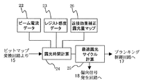
本発明の実施例1の荷電粒子線露光装置の最適露光クロック21,21aを計算するための制御回路の詳細を図3に示す。
ビットマップ変換回路15より転送されたビットマップデータ及びあらかじめ設定されたレジスト感度データ23と、あらかじめ設定もしくは測定されたビーム電流データ22より必要な露光時間計算24を行う。露光時間が計算されると、露光時間に基づいた最適露光サイクル21,21aを最適露光サイクル計算25により計算し、個々のブランキング制御回路17に転送する。同時に露光サイクルが変化すると、荷電粒子線10の走査時間も変化するため、データは偏向信号発生回路18にも送られる。
以上の一連の動作は荷電粒子線10の1走査毎に行われ、走査ごとに露光サイクル21,21aの最適化が図られる。
以上の構成によるマルチ電子ビーム露光装置を用い描画を行ったところ、総ビーム電流1マイクロアンペア、7マイクロアンペアの何れの場合にも1時間要していた描画時間がビーム電流1マイクロアンペアの場合には1時間、7マイクロアンペアの場合には10分と大幅な向上を図ることが出来た。
なお、以上の本発明の実施例1においては荷電粒子線10の走査毎に露光サイクル21,21aを計算していたが、描画前にビーム電流データ、レジスト感度データから最適露光サイクル21,21aを計算し設定する方法、また偏向器の偏向領域ごとに露露光サイクル21,21aを計算する方法の他、決められた露光領域ごとに最適露光サイクル21,21aを計算し設定する方法を用いても同様の効果をあげることが出来る。
FIG. 3 shows details of a control circuit for calculating
Necessary
The above series of operations is performed for each scanning of the
Was subjected to drawing using a multi-electron beam exposure apparatus according to the above configuration, the total beam current 1 microampere, 7 drawing time was also spent one hour in the case of any of microamps when the beam current 1 microampere In the case of 1 hour and 7 microamperes, a significant improvement of 10 minutes was achieved.
In the first embodiment of the present invention described above, the exposure cycles 21 and 21a are calculated for each scanning of the charged
次に、図4を参照して本発明の実施例2の荷電粒子線露光装置を説明する。
本発明の実施例1においてはビーム電流とレジスト感度によって露光時間、露光サイクル21,21aを決定する方法を説明したが、本実施例2ではさらに近接効果補正による影響を考慮した方式について説明する。
図4に本実施例2を説明するための最適クロックを設定する回路を示す。
ビットマップ変換回路15より転送されたビットマップデータ及びあらかじめ設定されたレジスト感度データ23、あらかじめ設定、もしくは測定されたビーム電流データ22、あらかじめ計算された近接効果補正データ25より必要な露光時間計算を24により行う。露光時間の計算は、荷電粒子線のビーム電流、レジスト感度及び近接補正値のうちの少なくとも1つに基づいて行うことも可能である。露光時間が計算されると、露光時間に基づいた最適露光サイクル21,21aを最適露光サイクル計算25により計算し、個々のブランキング制御回路17に転送する。
以上の一連の動作はビームの1走査毎に行われ、露光サイクル21,21aの計算、最適化が図られる。また、1走査内の各ピクセルの露光量は近接効果補正によって増減するが、露光サイクルは1走査内の最大露光量によって規定される。また同時に露光サイクル21,21aが変化すると、ビームの走査時間も変化するため、データは偏向信号発生回路18にも送られる。
以上の構成によるマルチ電子ビーム露光装置を用い近接効果補正描画を行ったところ、総ビーム電流1マイクロアンペア、7マイクロアンペアの何れも場合にも1時間要していた描画時間がビーム電流1マイクロアンペアの場合には1時間、7マイクロアンペアの場合には9分と大幅な向上を図ることが出来た。
なお、以上の説明ではビームの走査毎に露光サイクル21,21aを計算していたが、描画前にビーム電流データ、レジスト感度データ、近接効果補正データから走査毎の最適露光サイクル21,21aを計算し設定する方法、また偏向器の偏向領域ごとに最適露光サイクル21,21aを計算する方法の他、決められた露光領域ごとに最適露光サイクル21,21aを計算し設定する方法を用いても各方式に応じたデータ、記憶領域を用意することによって同様の効果をあげることが出来る。
また近接効果補正に限らず、露光量補正データを同様に最適露光サイクル計算25に適用することによって本実施例2と同様の効果をあげることが出来る。
Next, a charged particle beam exposure apparatus according to a second embodiment of the present invention will be described with reference to FIG.
In the first embodiment of the present invention, the method for determining the exposure time and the exposure cycles 21 and 21a based on the beam current and the resist sensitivity has been described. In the second embodiment, a method that further considers the influence of proximity effect correction will be described.
FIG. 4 shows a circuit for setting an optimum clock for explaining the second embodiment.
The required exposure time is calculated from the bitmap data transferred from the
The series of operations described above are performed for each scanning of the beam, and the exposure cycles 21 and 21a are calculated and optimized. The exposure amount of each pixel in one scan is increased or decreased by proximity effect correction, but the exposure cycle is defined by the maximum exposure amount in one scan. At the same time, when the exposure cycles 21 and 21a change, the beam scanning time also changes, so that the data is also sent to the deflection
When the proximity effect correction drawing was performed using the multi-electron beam exposure apparatus having the above configuration, the drawing time required 1 hour in both cases of the total beam current of 1 microampere and 7 microamperes, and the beam current of 1 microampere. In the case of, 1 hour was achieved, and in the case of 7 microamperes, it was 9 minutes.
In the above description, the exposure cycles 21 and 21a are calculated for each beam scan. However, the optimum exposure cycles 21 and 21a for each scan are calculated from the beam current data, resist sensitivity data, and proximity effect correction data before drawing. In addition to the method of calculating and setting the optimum exposure cycles 21 and 21a for each deflection area of the deflector, the method of calculating and setting the optimum exposure cycles 21 and 21a for each predetermined exposure area may be used. The same effect can be obtained by preparing data and storage areas according to the method.
Further, not only the proximity effect correction but also the exposure effect correction data can be applied to the optimum
次に、本発明の実施例3として、上記実施例1に係る荷電粒子線露光装置を利用した半導体デバイスの製造プロセスを説明する。
図5は半導体デバイスの全体的な製造プロセスのフローを示す図である。ステップ1(回路設計)では半導体デバイスの回路設計を行う。ステップ2(EBデータ変換)では設計した回路パターンに基づいて露光装置の露光制御データを作成する。
一方、ステップ3(ウエハ製造)ではシリコン等の材料を用いてウエハを製造する。ステップ4(ウエハプロセス)は前工程と呼ばれ、上記露光制御データが入力された露光装置とウエハを用い、リソグラフィ技術を利用してウエハ上に実際の回路を形成する。次のステップ5(組み立て)は後工程と呼ばれ、ステップ4によって作製されたウエハを用いて半導体チップ化する工程であり、アッセンブリ工程(ダイシング、ボンディング)、パッケージング工程(チップ封入)等の組み立て工程を含む。ステップ6(検査)ではステップ5で作製された半導体デバイスの動作確認テスト、耐久性テスト等の検査を行う。こうした工程を経て半導体デバイスが完成し、ステップ7でこれを出荷する。
上記ステップ4のウエハプロセスは以下のステップを有する。ウエハの表面を酸化させる酸化ステップ、ウエハ表面に絶縁膜を成膜するCVDステップ、ウエハ上に電極を蒸着によって形成する電極形成ステップ、ウエハにイオンを打ち込むイオン打ち込みステップ、ウエハに感光剤を塗布するレジスト処理ステップ、上記の露光装置によって回路パターンをレジスト処理ステップ後のウエハに焼付け露光する露光ステップ、露光ステップで露光したウエハを現像する現像ステップ、現像ステップで現像したレジスト像以外の部分を削り取るエッチングステップ、エッチングが済んで不要となったレジストを取り除くレジスト剥離ステップ。これらのステップを繰り返し行うことによって、ウエハ上に多重に回路パターンを形成する。
Next, as Example 3 of the present invention, a semiconductor device manufacturing process using the charged particle beam exposure apparatus according to Example 1 will be described.
FIG. 5 is a diagram showing a flow of an entire manufacturing process of a semiconductor device. In step 1 (circuit design), a semiconductor device circuit is designed. In step 2 (EB data conversion), exposure control data for the exposure apparatus is created based on the designed circuit pattern.
On the other hand, in step 3 (wafer manufacture), a wafer is manufactured using a material such as silicon. Step 4 (wafer process) is called a pre-process, and an actual circuit is formed on the wafer using lithography using the exposure apparatus and wafer to which the exposure control data has been input. The next step 5 (assembly) is called a post-process, and is a process for forming a semiconductor chip using the wafer produced in step 4, and is an assembly process (dicing, bonding), packaging process (chip encapsulation), etc. Process. In step 6 (inspection), the semiconductor device manufactured in step 5 undergoes inspections such as an operation confirmation test and a durability test. A semiconductor device is completed through these processes, and is shipped in Step 7.
The wafer process in step 4 includes the following steps. An oxidation step for oxidizing the surface of the wafer, a CVD step for forming an insulating film on the wafer surface, an electrode formation step for forming electrodes on the wafer by vapor deposition, an ion implantation step for implanting ions on the wafer, and applying a photosensitive agent to the wafer The resist processing step, the exposure step for printing and exposing the circuit pattern onto the wafer after the resist processing step by the above-described exposure apparatus, the development step for developing the wafer exposed in the exposure step, and the etching for removing portions other than the resist image developed in the development step Step, resist stripping step to remove resist that is no longer needed after etching. By repeating these steps, multiple circuit patterns are formed on the wafer.
1 電子源 2 コリメータレンズ
3 マスク 4 レンズアレイ
5 偏向器 6 ブランキングアレイ
7、8 レンズ 9 ブランキング絞り
10 荷電粒子線 11 試料
12 コントローラ 13 レンズ制御回路
14 描画パターン発生回路 15 ビットマップ変換回路
16 露光時間制御回路 17 ブランキング制御回路
18 偏向信号発生回路 19 偏向アンプ
20 露光時間 21,21a 露光サイクル
22 ビーム電流データ 23 レジスト感度データ
24 露光時間計算 25 最適露光サイクル計算
26 近接効果補正露光量マップ
DESCRIPTION OF SYMBOLS 1 Electron source 2 Collimator lens 3 Mask 4 Lens array 5
Claims (4)
前記ビームを偏向し、前記ビームの前記試料上への照射を制御するブランキング手段と、
前記ビームを偏向し、前記ビームを前記試料上で走査させる偏向器と、を備え、
前記ブランキング手段および前記偏向器は、前記ビームが前記試料上に照射される時間と前記ビームが前記試料上に照射されない時間の和で表される露光サイクルで動作し、
前記露光サイクルは、ビーム電流データ、レジスト感度データおよび近接効果補正データより前記ビームが前記試料上に照射される時間を求め、その結果に応じて前記ビームが前記試料上に照射されない時間を小さくするように、可変に設定されることを特徴とする荷電粒子線露光装置。 A charged particle beam exposure apparatus for performing exposure by irradiating a sample coated with a resist with a beam from a charged particle source,
And blanking means for said deflecting the beam to control the irradiation onto the sample in the beam,
A deflector that deflects the beam and scans the beam over the sample;
Said blanking means and the deflector operates at an exposure cycle time and the beam the beam is irradiated onto the sample is represented by the sum of time that is not irradiated onto the sample,
In the exposure cycle, the time during which the beam is irradiated onto the sample is obtained from beam current data, resist sensitivity data, and proximity effect correction data, and the time during which the beam is not irradiated onto the sample is reduced according to the result. As described above, the charged particle beam exposure apparatus is variably set.
Priority Applications (1)
| Application Number | Priority Date | Filing Date | Title |
|---|---|---|---|
| JP2005075830A JP4761508B2 (en) | 2005-03-16 | 2005-03-16 | Charged particle exposure apparatus and device manufacturing method |
Applications Claiming Priority (1)
| Application Number | Priority Date | Filing Date | Title |
|---|---|---|---|
| JP2005075830A JP4761508B2 (en) | 2005-03-16 | 2005-03-16 | Charged particle exposure apparatus and device manufacturing method |
Publications (3)
| Publication Number | Publication Date |
|---|---|
| JP2006261342A JP2006261342A (en) | 2006-09-28 |
| JP2006261342A5 JP2006261342A5 (en) | 2008-04-24 |
| JP4761508B2 true JP4761508B2 (en) | 2011-08-31 |
Family
ID=37100253
Family Applications (1)
| Application Number | Title | Priority Date | Filing Date |
|---|---|---|---|
| JP2005075830A Expired - Fee Related JP4761508B2 (en) | 2005-03-16 | 2005-03-16 | Charged particle exposure apparatus and device manufacturing method |
Country Status (1)
| Country | Link |
|---|---|
| JP (1) | JP4761508B2 (en) |
Families Citing this family (23)
| Publication number | Priority date | Publication date | Assignee | Title |
|---|---|---|---|---|
| JP5283410B2 (en) * | 2008-03-26 | 2013-09-04 | 富士フイルム株式会社 | Electron beam drawing method, fine pattern drawing system, method of manufacturing concave / convex pattern carrier, and method of manufacturing magnetic disk medium |
| JP5826566B2 (en) | 2011-09-01 | 2015-12-02 | 株式会社ニューフレアテクノロジー | Multi-charged particle beam writing apparatus and multi-charged particle beam writing method |
| JP5859778B2 (en) | 2011-09-01 | 2016-02-16 | 株式会社ニューフレアテクノロジー | Multi-charged particle beam writing apparatus and multi-charged particle beam writing method |
| TWI477925B (en) * | 2011-10-04 | 2015-03-21 | Nuflare Technology Inc | Multi - beam charged particle beam mapping device and multi - beam charged particle beam rendering method |
| JP5977941B2 (en) | 2011-12-19 | 2016-08-24 | 株式会社ニューフレアテクノロジー | Multi-charged particle beam writing apparatus and multi-charged particle beam writing method |
| JP5970213B2 (en) | 2012-03-19 | 2016-08-17 | 株式会社ニューフレアテクノロジー | Multi-charged particle beam writing apparatus and multi-charged particle beam writing method |
| JP6014342B2 (en) | 2012-03-22 | 2016-10-25 | 株式会社ニューフレアテクノロジー | Multi-charged particle beam writing apparatus and multi-charged particle beam writing method |
| JP5956797B2 (en) * | 2012-03-22 | 2016-07-27 | 株式会社ニューフレアテクノロジー | Multi-charged particle beam writing apparatus and multi-charged particle beam writing method |
| JP5977550B2 (en) | 2012-03-22 | 2016-08-24 | 株式会社ニューフレアテクノロジー | Multi charged particle beam lithography system |
| JP6147528B2 (en) | 2012-06-01 | 2017-06-14 | 株式会社ニューフレアテクノロジー | Multi-charged particle beam writing method and multi-charged particle beam writing apparatus |
| JP6013089B2 (en) * | 2012-08-30 | 2016-10-25 | 株式会社ニューフレアテクノロジー | Charged particle beam drawing method and charged particle beam drawing apparatus |
| JP6215586B2 (en) | 2012-11-02 | 2017-10-18 | 株式会社ニューフレアテクノロジー | Multi-charged particle beam writing method and multi-charged particle beam writing apparatus |
| JP6057700B2 (en) | 2012-12-26 | 2017-01-11 | 株式会社ニューフレアテクノロジー | Multi charged particle beam lithography system |
| JP6080540B2 (en) | 2012-12-26 | 2017-02-15 | 株式会社ニューフレアテクノロジー | Charged particle beam lithography system |
| JP6061741B2 (en) | 2013-03-13 | 2017-01-18 | 株式会社ニューフレアテクノロジー | Multi-beam current adjustment method |
| TWI533096B (en) | 2013-05-24 | 2016-05-11 | Nuflare Technology Inc | Multi - charged particle beam mapping device and multi - charged particle beam rendering method |
| JP6190254B2 (en) | 2013-12-04 | 2017-08-30 | 株式会社ニューフレアテクノロジー | Multi-charged particle beam writing apparatus and multi-charged particle beam writing method |
| JP6262024B2 (en) | 2014-03-04 | 2018-01-17 | 株式会社ニューフレアテクノロジー | Multi charged particle beam lithography system |
| JP2015201576A (en) | 2014-04-09 | 2015-11-12 | 株式会社ニューフレアテクノロジー | Shot data generation method and multi-charged particle beam lithography method |
| US9390891B2 (en) * | 2014-08-15 | 2016-07-12 | Taiwan Semiconductor Manufacturing Company, Ltd. | Apparatus for charged particle lithography system |
| JP2016122676A (en) | 2014-12-24 | 2016-07-07 | 株式会社アドバンテスト | Exposure device and exposure method |
| JP2017143187A (en) * | 2016-02-10 | 2017-08-17 | 株式会社ニューフレアテクノロジー | Evaluation method for molding aperture array |
| JP6804389B2 (en) * | 2017-05-30 | 2020-12-23 | 株式会社ニューフレアテクノロジー | Drawing device and drawing method |
Family Cites Families (3)
| Publication number | Priority date | Publication date | Assignee | Title |
|---|---|---|---|---|
| JP3419913B2 (en) * | 1994-11-14 | 2003-06-23 | 富士通株式会社 | Charged particle beam exposure method and apparatus |
| JP3236162B2 (en) * | 1994-03-18 | 2001-12-10 | 富士通株式会社 | Charged particle beam exposure method and apparatus |
| JP2005032888A (en) * | 2003-07-10 | 2005-02-03 | Nikon Corp | Device and method for charged particle beam exposure |
-
2005
- 2005-03-16 JP JP2005075830A patent/JP4761508B2/en not_active Expired - Fee Related
Also Published As
| Publication number | Publication date |
|---|---|
| JP2006261342A (en) | 2006-09-28 |
Similar Documents
| Publication | Publication Date | Title |
|---|---|---|
| JP4761508B2 (en) | Charged particle exposure apparatus and device manufacturing method | |
| JP5116996B2 (en) | Charged particle beam drawing method, exposure apparatus, and device manufacturing method | |
| US6835937B1 (en) | Correcting method for correcting exposure data used for a charged particle beam exposure system | |
| US6137113A (en) | Electron beam exposure method and apparatus | |
| US7388214B2 (en) | Charged-particle beam exposure apparatus and method | |
| US11037759B2 (en) | Multi charged particle beam writing apparatus and multi charged particle beam writing method | |
| JP2002075830A (en) | Charged-particle beam exposure method, reticle and manufacturing method of device | |
| JP4458372B2 (en) | Multi-beam charged particle beam apparatus, multi-beam charged particle beam control method and device manufacturing method | |
| US8692218B2 (en) | Charged particle beam exposure apparatus | |
| US7049610B2 (en) | Charged particle beam exposure method, charged particle beam exposure apparatus, and device manufacturing method | |
| US7005659B2 (en) | Charged particle beam exposure apparatus, charged particle beam exposure method, and device manufacturing method using the same apparatus | |
| CN109923479B (en) | Fabrication of unique chips using charged particle multi-beam lithography system | |
| JP4804136B2 (en) | Charged particle beam apparatus and device manufacturing method | |
| JP3080006B2 (en) | Electron beam exposure correction method | |
| JP2006019434A (en) | Charged particle beam exposure method, charged particle beam exposure apparatus, and device manufacturing method | |
| US6337164B1 (en) | Charged-particle-beam microlithography methods exhibiting improved pattern-feature accuracy, and device manufacturing methods comprising same | |
| JP4356064B2 (en) | Charged particle beam exposure apparatus and device manufacturing method using the apparatus | |
| JP4494734B2 (en) | Charged particle beam drawing method, charged particle beam exposure apparatus, and device manufacturing method | |
| JP3976835B2 (en) | Electron beam exposure method and electron beam exposure apparatus | |
| JP2001244165A (en) | Method for correcting proximity effect, reticle, and method of manufacturing device | |
| CN114488706A (en) | Fabrication of unique chips using charged particle multi-beam lithography system | |
| JP4504060B2 (en) | Charged particle beam exposure system | |
| JP4804592B2 (en) | Charged particle beam apparatus and device manufacturing method | |
| JP2006019437A (en) | Charged particle beam exposure method, charged particle beam exposure apparatus, and device manufacturing method | |
| JP2002015975A (en) | Device and method for correcting proximity effect, and device producing method |
Legal Events
| Date | Code | Title | Description |
|---|---|---|---|
| A521 | Written amendment |
Free format text: JAPANESE INTERMEDIATE CODE: A523 Effective date: 20080307 |
|
| A621 | Written request for application examination |
Free format text: JAPANESE INTERMEDIATE CODE: A621 Effective date: 20080307 |
|
| RD02 | Notification of acceptance of power of attorney |
Free format text: JAPANESE INTERMEDIATE CODE: A7422 Effective date: 20080307 |
|
| A072 | Dismissal of procedure [no reply to invitation to correct request for examination] |
Free format text: JAPANESE INTERMEDIATE CODE: A072 Effective date: 20080625 |
|
| RD01 | Notification of change of attorney |
Free format text: JAPANESE INTERMEDIATE CODE: A7421 Effective date: 20090406 |
|
| RD04 | Notification of resignation of power of attorney |
Free format text: JAPANESE INTERMEDIATE CODE: A7424 Effective date: 20100201 |
|
| RD01 | Notification of change of attorney |
Free format text: JAPANESE INTERMEDIATE CODE: A7421 Effective date: 20100630 |
|
| A977 | Report on retrieval |
Free format text: JAPANESE INTERMEDIATE CODE: A971007 Effective date: 20110104 |
|
| A131 | Notification of reasons for refusal |
Free format text: JAPANESE INTERMEDIATE CODE: A131 Effective date: 20110111 |
|
| A521 | Written amendment |
Free format text: JAPANESE INTERMEDIATE CODE: A523 Effective date: 20110311 |
|
| TRDD | Decision of grant or rejection written | ||
| A01 | Written decision to grant a patent or to grant a registration (utility model) |
Free format text: JAPANESE INTERMEDIATE CODE: A01 Effective date: 20110531 |
|
| A01 | Written decision to grant a patent or to grant a registration (utility model) |
Free format text: JAPANESE INTERMEDIATE CODE: A01 |
|
| A61 | First payment of annual fees (during grant procedure) |
Free format text: JAPANESE INTERMEDIATE CODE: A61 Effective date: 20110606 |
|
| FPAY | Renewal fee payment (event date is renewal date of database) |
Free format text: PAYMENT UNTIL: 20140617 Year of fee payment: 3 |
|
| R150 | Certificate of patent or registration of utility model |
Free format text: JAPANESE INTERMEDIATE CODE: R150 |
|
| LAPS | Cancellation because of no payment of annual fees |