JP2015190853A - Method of manufacturing scintillator array - Google Patents
Method of manufacturing scintillator array Download PDFInfo
- Publication number
- JP2015190853A JP2015190853A JP2014068362A JP2014068362A JP2015190853A JP 2015190853 A JP2015190853 A JP 2015190853A JP 2014068362 A JP2014068362 A JP 2014068362A JP 2014068362 A JP2014068362 A JP 2014068362A JP 2015190853 A JP2015190853 A JP 2015190853A
- Authority
- JP
- Japan
- Prior art keywords
- scintillator
- resin
- array
- dual
- lattice
- Prior art date
- Legal status (The legal status is an assumption and is not a legal conclusion. Google has not performed a legal analysis and makes no representation as to the accuracy of the status listed.)
- Granted
Links
Images


Landscapes
- Conversion Of X-Rays Into Visible Images (AREA)
- Measurement Of Radiation (AREA)
Abstract
Description
本発明は、放射線検出器用のデュアルアレイ型のシンチレータアレイを効率良く製造する方法に関する。 The present invention relates to a method for efficiently manufacturing a dual array type scintillator array for a radiation detector.
放射線検査装置の1つにコンピュータ断層撮影装置[Computed Tomography(CT)装置]がある。CT装置は、X線ファンビームを放射するX線管と、多数の放射線検出素子を併設した放射線検出器とを有する。X線管と放射線検出器は、測定対象を中心にして対向するように配置される。X線管から放射されたX線ファンビームは測定対象を透過し、放射線検出器で検出される。照射角度の異なる測定対象のX線吸収データを収集し、コンピュータ解析により測定対象の断層面における個々の位置のX線吸収率を算出し、X線吸収率に応じた画像を構成する。放射線検出素子として、シンチレータと受光素子を組み合わせた検出器が用いられ、受光素子としてはシリコンフォトダイオードや光電子増倍管などが用いられている。前記放射線検出素子は多数配列して用いるため、予め複数のシンチレータを配列し、受光素子と組み合わせる一面以外の面を反射材で覆ったものをシンチレータアレイとして、放射線検出器に用いられている。 One of the radiation examination apparatuses is a computed tomography apparatus (Computed Tomography (CT) apparatus). The CT apparatus has an X-ray tube that emits an X-ray fan beam and a radiation detector that is provided with a large number of radiation detection elements. The X-ray tube and the radiation detector are arranged so as to face each other with the measurement object as the center. The X-ray fan beam emitted from the X-ray tube passes through the measurement object and is detected by the radiation detector. X-ray absorption data of a measurement target having different irradiation angles is collected, and an X-ray absorption rate at each position on the tomographic plane of the measurement target is calculated by computer analysis, and an image corresponding to the X-ray absorption rate is constructed. A detector that combines a scintillator and a light receiving element is used as the radiation detecting element, and a silicon photodiode, a photomultiplier tube, or the like is used as the light receiving element. Since a large number of the radiation detection elements are arranged and used, a plurality of scintillators are arranged in advance, and a surface other than the one combined with the light receiving element is covered with a reflecting material is used as a scintillator array in the radiation detector.
X線吸収率が異なる2のシンチレータのセルを用いたデュアルエネルギーの検出器は、例えば特許文献1及び特許文献2に開示されている。特許文献1は、一方のシンチレータセルの発光を一方のダイオードで受光し、他方のシンチレータセルの発光を他方のダイオードで受光するデュアルエネルギーの検出器を開示している。特許文献2は、上部及び下部のシンチレータ、第1及び第2の光検出器を有する放射線検出器であって、上部のシンチレータは、低エネルギーの放射線を光に変換し、高エネルギーの放射線を透過するようにX線源に対向して備えられ、下部のシンチレータは、高エネルギーの放射線を光に変換するように、X線源から上部のシンチレータより遠位側に、隣接して備えられ、上部及び下部のシンチレータの光をそれぞれ受け入れ、電気信号に変換するように第1及び第2の光検出器が光学的に結合された放射線検出器が開示されている。これらの検出器を利用することにより、X線のエネルギーごとに透過係数が異なる部位を透過した後のX線の強度を、分離しつつ、かつ同時に検出することができるため、一度のX線の照射で多くの情報を得ることができる。
For example,
特許文献3は、幅の異なるシンチレータセルを組合せた1次元又は多次元の検出器アレイを製造する方法を開示している。この方法は、(a)放射線に対して敏感な材料を含有するセンサ層及び基層からなる複合層を形成し、(b)センサ層を互いに絶縁された個々のエレメントに分割するために、基層と反対側から複合層の材料を切断することにより、隔壁をセンサ層に形成している。 Patent Document 3 discloses a method of manufacturing a one-dimensional or multi-dimensional detector array in which scintillator cells having different widths are combined. The method comprises (a) forming a composite layer consisting of a sensor layer and a base layer containing a material sensitive to radiation, and (b) dividing the sensor layer into individual elements that are insulated from one another. The partition wall is formed in the sensor layer by cutting the material of the composite layer from the opposite side.
特許文献4は、X線吸収率の異なる2つのシンチレータ素子がX線の透過方向に配置されており、各シンチレータ素子に対応する光検出素子がそのシンチレータ素子に垂直な方向に配置されており、複数のシンチレータ素子及び複数の光検出素子が列をなしているX線検出器アレイを開示している。ここで複数のシンチレータ素子は光反射性物質で一体的にモールドされている。
In
特許文献5は、シンチレーションセラミックのウェハを作製し、セラミックウェハの上面に直交する2方向の複数のスリットを形成し、セラミックウェハの表面の一部を酸化して反射層を形成することによりシンチレーションアレイを製造する方法を開示している。ここで個々のピクセルの間隙を形成するスリットも同様に反射層で充填される。
特許文献1及び2には、具体的なシンチレーションアレイの製造方法を開示していない。特許文献3の方法では、セルの数が増えるにつれて工数が増大してしまう。特許文献4も、X線検出器アレイの製造方法を具体的に開示していない。特許文献5に記載のシンチレーションアレイは1つのシンチレーションセラミックにより形成するものであり、2つのシンチレーションセルを配列する技術を開示していない。
本発明の目的は、X線吸収率が異なる2つのシンチレータセルを用いたデュアルアレイ型のシンチレータアレイを、効率良く製造する方法を提供することである。 An object of the present invention is to provide a method for efficiently manufacturing a dual array type scintillator array using two scintillator cells having different X-ray absorption rates.
本発明のシンチレータアレイの製造方法は、デュアルアレイ型のシンチレータアレイを製造する方法であって、第1のシンチレータ及び第2のシンチレータの基板を、反射材用樹脂層を介して積層し、積層基板を形成する積層工程と、前記積層基板に格子状の溝を形成して、第1及び第2のシンチレータのセルが前記反射材用樹脂層を介して積層した形状を有するデュアルセルが林立した格子状溝付き積層基板を形成する溝加工工程と、少なくとも前記格子状の溝に反射材用樹脂を充填し、デュアルセルアレイ集合体を形成する樹脂充填工程と、前記格子状の溝のうち、一方向反射材用樹脂を充填した溝に沿って切断し、デュアルセルアレイ集合体から、デュアルセルが配列したデュアルセルアレイを切り離す分離工程と、を有する。 The method of manufacturing a scintillator array of the present invention is a method of manufacturing a dual array type scintillator array, in which a substrate of a first scintillator and a second scintillator are stacked via a resin layer for a reflector, and a stacked substrate And a lattice in which dual cells having a shape in which a lattice-like groove is formed in the laminated substrate and the cells of the first and second scintillators are laminated via the resin layer for the reflector are formed. A groove processing step for forming a laminated substrate with grooved grooves, a resin filling step for forming a dual cell array assembly by filling at least the lattice-shaped grooves with a resin for a reflector, and one direction among the lattice-shaped grooves And a separation step of cutting along the groove filled with the resin for reflecting material and separating the dual cell array in which the dual cells are arranged from the dual cell array assembly.
前記溝加工工程において、第1及び第2のシンチレータのうち、溝の深さ方向の深部側にあるシンチレータの一部を連結部として残留させ、前記分離工程の前もしくは後で、前記デュアルセルアレイ集合体を、前記溝の深さ方向の逆方向から除去していき、連結部を除去することが好ましい。 In the groove processing step, of the first and second scintillators, a part of the scintillator on the deep side in the groove depth direction is left as a connecting portion, and before or after the separation step, the dual cell array assembly It is preferable that the body is removed from the direction opposite to the depth direction of the groove to remove the connecting portion.
さらに、前記分離工程において、前記格子状の溝に充填した反射材用樹脂をデュアルセルアレイ近傍に残して切断することが好ましい。 Furthermore, in the separation step, it is preferable that the reflector resin filled in the lattice-like grooves is cut in the vicinity of the dual cell array.
前記分離工程後にデュアルセルアレイに反射材用樹脂を追加形成する反射材形成工程を有することが好ましい。 It is preferable to have a reflecting material forming step of additionally forming a resin for the reflecting material in the dual cell array after the separating step.
前記樹脂充填工程において、格子状溝付き積層基板を支持プレートに接着し、支持することが好ましい。 In the resin filling step, it is preferable that the laminated substrate with grid-like grooves is bonded and supported on a support plate.
前記樹脂充填工程において、前記支持プレートに接着する際に熱剥離型の接着シートを使用することが好ましい。 In the resin filling step, it is preferable to use a heat-peelable adhesive sheet when bonding to the support plate.
本発明の方法によれば、2のシンチレータを用いたデュアルアレイ型のシンチレータアレイを、効率良く製造することができる。特に、格子状の溝によって2のシンチレータの位置を同時に決めることができ、位置決めのための手間を省けることが優れている。 According to the method of the present invention, a dual-array scintillator array using two scintillators can be efficiently manufactured. In particular, the position of the two scintillators can be determined simultaneously by the grid-like grooves, and it is excellent in that the labor for positioning can be saved.
本発明の実施形態を図面を参照して以下詳細に説明するが、本発明はそれらに限定されるものではない。各実施形態の説明は、特に断りがなければ他の実施形態にも適用される。 Embodiments of the present invention will be described below in detail with reference to the drawings, but the present invention is not limited thereto. The description of each embodiment is applicable to other embodiments unless otherwise specified.
以下の説明では、X線のエネルギーごとに透過係数が異なる部位を透過した後のX線の強度を、分離しつつ、かつ同時に検出できる検出器を構成するためのシンチレータアレイをデュアルアレイ型のシンチレータアレイとしている。第1のシンチレータは、第2のシンチレータとはX線吸収率が異なり、例えば材料組成や厚さ寸法などが異なっている。そして、X線照射方向に沿ってX線が照射される基板面積を同じにして、単位体積あたりのX線吸収率を比較した場合、第2のシンチレータのX線吸収率は、第1のシンチレータのX線吸収率よりも高いことが好ましい。なお、前記X線吸収率は、第1又は第2のシンチレータに照射した全波長域のX線と、前記全波長域のX線のうち第1又は第2のシンチレータで吸収されたX線とに係る強度の比率に相当する。そして、与えられるエネルギー(或いはそれに対応するX線の波長)によって、X線吸収率の大きさは変わる。 In the following description, a scintillator array for constructing a detector that can simultaneously detect X-ray intensities after passing through a site having a different transmission coefficient for each X-ray energy and that can be detected simultaneously is a dual-array scintillator. It is an array. The first scintillator is different in X-ray absorption rate from the second scintillator, for example, in material composition, thickness dimension, and the like. When the X-ray absorption rate per unit volume is compared with the same substrate area irradiated with X-rays along the X-ray irradiation direction, the X-ray absorption rate of the second scintillator is the first scintillator. It is preferably higher than the X-ray absorption rate. The X-ray absorptance is the X-rays of the entire wavelength region irradiated to the first or second scintillator and the X-rays absorbed by the first or second scintillator among the X-rays of the entire wavelength region. It corresponds to the ratio of the strength according to. And the magnitude | size of an X-ray absorption rate changes with the energy (or wavelength of X-ray corresponding to it) given.
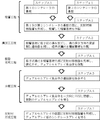
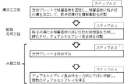
[1]第1の実施形態
第1の実施形態による製造方法のフローチャートを図1に示す。本発明の第1の実施形態は、大きく分けて積層工程、溝加工工程、樹脂充填工程、分離工程の4つの工程を経てデュアルアレイ型のシンチレータアレイが形成される。デュアルアレイ型のシンチレータアレイとは、異なるエネルギーのX線を検出するために、X線吸収率の異なる2のシンチレータを用いて、X線透過方向に第1のシンチレータのセル及び第2のシンチレータのセルを上下2段に配置したデュアルセルが、所定の位置に複数配列されているシンチレータアレイである。以下の説明では、X線が透過する方向、すなわちシンチレータのセルを上下2段に配置した方向をZ方向とし、それに対して垂直であって、複数の第1のシンチレータのセル及び第2のシンチレータのセルが配列している方向をY方向とし、Z方向及びY方向に対して垂直な方向をX方向とする。また、セルとは単位体積あたりのX線を検出するシンチレータ素子を示し、受光素子と組み合わせることによって放射線検出器を構成する。
[1] First Embodiment FIG. 1 shows a flowchart of a manufacturing method according to a first embodiment. In the first embodiment of the present invention, a dual array type scintillator array is formed through four steps of a lamination process, a groove processing process, a resin filling process, and a separation process. In order to detect X-rays having different energies, the dual array type scintillator array uses two scintillators having different X-ray absorption rates, and uses the first scintillator cell and the second scintillator in the X-ray transmission direction. This is a scintillator array in which a plurality of dual cells in which cells are arranged in two upper and lower stages are arranged at predetermined positions. In the following description, the direction in which X-rays are transmitted, that is, the direction in which the scintillator cells are arranged in two upper and lower stages is defined as the Z direction, and is perpendicular to the first direction. A direction in which the cells are arranged is a Y direction, and a direction perpendicular to the Z direction and the Y direction is an X direction. A cell indicates a scintillator element that detects X-rays per unit volume, and constitutes a radiation detector by being combined with a light receiving element.
シンチレータアレイのセルは、透過したX線を正確に検出するために、前記第1のシンチレータ及び第2のシンチレータの高い位置精度が要求される。本発明では、積層工程において、上下2段の第1のシンチレータ及び第2のシンチレータの間隔(Z方向の距離)を決め、溝加工工程においてX線透過方向と垂直な方向(Y方向及びX方向)の位置精度を得ている。このとき、複数の列を同時に形成できるように、第1のシンチレータの基板及び第2のシンチレータの基板は十分な面積を有することが好ましい。それにより、樹脂充填工程及び分離工程では複数のシンチレータアレイの反射材を同時に形成できる。そのため、第1のシンチレータのセル及び第2のシンチレータのセルを一つずつ配列してシンチレータアレイを製造するより、効率良く製造できる。 The cells of the scintillator array are required to have high positional accuracy of the first scintillator and the second scintillator in order to accurately detect transmitted X-rays. In the present invention, in the stacking step, the distance between the first and second scintillators in the upper and lower stages (distance in the Z direction) is determined, and in the grooving step, the direction perpendicular to the X-ray transmission direction (Y direction and X direction). ) Position accuracy is obtained. At this time, it is preferable that the substrate of the first scintillator and the substrate of the second scintillator have a sufficient area so that a plurality of rows can be formed simultaneously. Thereby, a plurality of scintillator array reflectors can be formed simultaneously in the resin filling step and the separation step. Therefore, the first scintillator cell and the second scintillator cell are arranged one by one, and the scintillator array can be manufactured more efficiently.
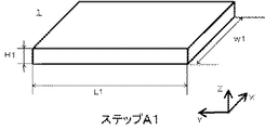
まず、積層工程について以下に説明する。最初に、ステップA1にて積層に使用する第1のシンチレータの基板1及び第2のシンチレータの基板2を準備する。前記第1のシンチレータ及び第2のシンチレータは、位置決めの際に変形したり、加工時に動くことの無い程度の硬度を有する材料で構成することが好ましい。例えば高密度、高硬度のセラミックス材料などのシンチレータが好ましい。また、使用するシンチレータの材料に応じて、加工精度が良く、加工時間の短い加工方法を選択することが好ましい。例えば前記セラミックス材料を用いる場合、ダイヤ等の砥粒を用いた回転砥石による加工や、ワイヤーソーによる加工方法を選択することが好ましい。
First, the lamination process will be described below. First, in step A1, a
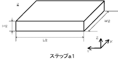
積層工程の一例として、図2に第1のシンチレータの基板1(以下、基板1という)、図3に第2のシンチレータの基板2(以下、基板2という)を示す。基板は図示したように矩形形状であれば、加工などによって切り落とすなどのシンチレータアレイとして使用しない領域を減らせるため好ましい。基板1のY方向の辺L1は、完成後のシンチレータアレイにおいてセルが並ぶY方向の辺の長さより長いことが好ましい。さらに基板1のY方向の辺の長さL1と基板2のY方向の辺の長さL2が同じ長さである方が、シンチレータアレイとして使用しない領域を減らせるため好ましい。また、基板1のX方向の幅W1、及び基板2のX方向の幅W2についてはシンチレータアレイの取れ数に応じて任意に決定することができるが、Y方向の辺の長さと同様に、同じ長さである方が、シンチレータアレイとして使用しない領域を減らせるため好ましい。
As an example of the stacking process, FIG. 2 shows a
基板1、2のZ方向の辺の高さH1及びH2については、シンチレータアレイの第1のシンチレータのセル及び第2のシンチレータのセルのZ方向の設計寸法に応じて任意に決めることができる。また、溝加工工程において基板1または基板2に、連結部を設ける場合には、基板1または基板2のZ方向寸法を大きめに設定しても良い。ここでは、基板2に連結部を設けるためにH2を、シンチレータアレイの第2のシンチレータのセルのZ方向の寸法より大きめに設定した。前記H2は連結部21として残した際の強度を考慮した上で、できるだけ小さくしておくほうが連結部21の研削時間の短縮や、加工による廃棄部分が少なくて済むため好ましい。
The heights H1 and H2 of the sides in the Z direction of the
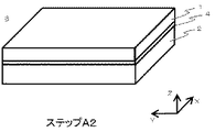
次に、ステップA2において、第1および第2のシンチレータの基板の間に、反射材用樹脂層4を形成し、反射材用樹脂層4を介して基板1と基板2を積層して接合した積層基板3を図4に示す。反射材用樹脂層4は、第1のシンチレータの蛍光周波数領域、及び第2のシンチレータの蛍光周波数領域の、両方の周波数領域で、反射率が高く、且つ、基板1及び基板2の位置がずれないように固定できることが望ましい。例えば、可視光の周波数領域における屈折率の高い酸化チタンの微粒子を混合した液状熱硬化性エポキシ樹脂などを用いることができる。例えば、第1のシンチレータと第2のシンチレータとの間隔を正確に決めるために、液状の反射材用樹脂を用いて、スクリーン印刷、バーコーター、スピンコーター、スプレーコーターなどの一定の厚さで均一に塗布できる方法を用いて、正確な寸法の反射材用樹脂層4を形成することが望ましい。前述したいずれかの方法で、基板2に、一定の厚さで形成した液状の反射材用樹脂を硬化した後、前記硬化した樹脂の上に液状の樹脂を薄く塗布して、基板1を接合する方法や、基板1又は基板2に正確な寸法の反射材用樹脂層4を形成した後に、一定の間隔で維持できるピンやボール等を基板間に挟み、支持しながら硬化する方法でも良い。以上の方法等により、積層工程においてデュアルセルの、第1のシンチレータ及び第2のシンチレータの正確なZ方向の寸法を決める。
Next, in step A2, the reflective
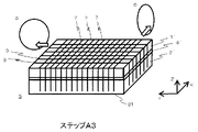
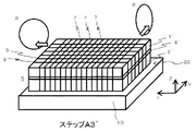
次にステップA3の溝加工工程について説明する。溝加工工程では、第1のシンチレータのセル1´及び第2のシンチレータのセル2´の形成と、シンチレータアレイにおけるセルの間の寸法を決めること、を同時に行うことを目的として、前記積層基板3に格子状の溝を形成して、第1及び第2のシンチレータのセルが前記反射材用樹脂層4を介して積層した形状を有するデュアルセルが林立した格子状溝付き積層基板を形成する。それによりシンチレータアレイのセルの簡易的な位置決め手法として、加工そのものを利用できるため、効率を上げることができる。
Next, the grooving process of step A3 will be described. In the grooving step, for the purpose of simultaneously forming the
図5のように砥石8を用いて溝9を形成し、溝とセルとのX方向の正確な寸法を決め、砥石6を用いて溝7を形成し、溝とセルとのY方向の正確な寸法を決めることで、シンチレータアレイにおけるセルの位置を精度良く決めることができる。ここで溝とはセル間の空隙を示しており、格子状溝付き積層基板におけるデュアルセル間に形成する反射材を充填するための空隙のことである。加工の方法は、基板の加工に用いた方法と同じく、使用するシンチレータ基板の材料に応じて、加工精度が良く、加工時間の短い方法で行なうことが好ましい。加工手段としては回転砥石以外に、格子状に平行な複数の溝を形成するため、複数のワイヤーを張ったマルチワイヤーソーなどを用いて同時に溝を形成すると、効率が良くなるため好ましい。また、回転砥石を用いる場合、プログラム制御可能なダイシングマシンなどを用いることで、加工精度をさらに高めつつ、かつ複数の平行な溝を効率的に加工できるため好ましい。溝9は隣り合うシンチレータアレイを、受光面と背面反射材面とに切り離すために、溝7とは異なる寸法で加工しても良い。
As shown in FIG. 5, the grindstone 8 is used to form the groove 9, the exact dimension of the groove and the cell in the X direction is determined, the grindstone 6 is used to form the
加工方法として、例えば回転砥石などを用い、シンチレータアレイのセルの間の寸法に合わせた幅の回転砥石6を用いてX方向の溝7を形成し、X方向に形成する反射材用樹脂の厚さと分離工程における切りしろを考慮した幅の回転砥石8を使用してY方向の溝9を形成する。正確な溝幅を形成できる加工方法を選択することで、積層基板3に正確な寸法の格子状の溝が形成でき、かつ溝の深さ方向の深部側にあるシンチレータの一部を連結部21として残留させることでシンチレータセルの位置が決められた格子状溝付き積層基板5を作製できる。格子状溝付き積層基板5は格子状溝付き第1のシンチレータ1´、格子状溝付き第2のシンチレータ2´、格子状溝付き樹脂層4´から構成される。
As a processing method, for example, a rotating grindstone is used, and a
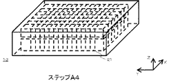
次にステップA4において樹脂充填工程を進める。この工程では、前記格子状の溝に反射材用樹脂を充填し、デュアルセルアレイ集合体を形成する。溝加工工程において連結部21による位置決めがなされており、格子状の溝とセルの位置を正確に維持したまま、反射材用樹脂を充填できるため、位置精度の高いデュアルセルアレイ集合体を形成できる。例えば、図6のように支持プレート10と型枠11を用いて、型枠内に液状の反射材用樹脂12を流し込み、溝内に反射材用樹脂12を充填する。また、支持プレート10及び型枠11は樹脂が付着しても剥離しやすいように、フッ素樹脂等のフィルムやテープで表面を覆ったり、あるいは支持プレート10や型枠11そのものをフッ素樹脂等で構成することが好ましい。あるいは、林立したデュアルセルの周囲に、シンチレータアレイのセルとして使用しない部分を有した格子状溝付き積層基板である場合、支持プレート10を使用せず型枠11だけで前記格子状溝付き積層基板を囲い、溝内に反射材用樹脂を充填しても良い。充填する樹脂は積層工程で用いた樹脂と同様に第1のシンチレータ及び第2のシンチレータの発光を効率よく反射できる反射材用樹脂が好ましい。充填した樹脂が硬化した後に、支持プレート10や型枠11を取り除き、図7に示すデュアルセルアレイ集合体13を得る。
Next, the resin filling process is advanced in step A4. In this step, the lattice-shaped grooves are filled with a resin for reflecting material to form a dual cell array assembly. Positioning by the connecting
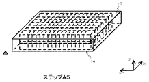
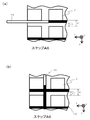
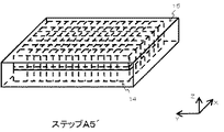
ステップA5で、分離工程の切断するときの格子状の溝の位置を確認するために、溝に充填した反射材用樹脂が見えるように連結部21を加工する。このときの加工方法は基板を加工したときと同様にダイヤの回転砥石などで連結部を切断して除去しても良い。また、格子状の溝の深さ方向の逆方向から連結部を除去していく方法として、平面を加工できる平面研削機や縦型研削機などを用いて、図8のように連結部を研削して除去しても良い。さらに、遊離砥粒を用いた研磨加工して除去しても良く、この場合、樹脂を同時に加工しても固定砥粒のような被加工物の目詰まりを起こしにくい。得られた樹脂充填溝付き積層基板13の上面15が平坦になっていない場合、先に上面を同様の方法で加工して平面にしておくことで、底面14を加工し易くなる。
In step A5, in order to confirm the position of the grid-like groove when the separation step is cut, the connecting
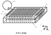
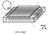
次に、ステップA6では、図9に示すように、ステップA5で加工したデュアルセルアレイ集合体13を反転し、底面14を上にして樹脂充填溝9´の位置を確認しながら回転砥石16で切断し、デュアルセルアレイを得る。このときに切断位置を図10(a)に示すように、底面14から見える第2のシンチレータのセル2´と反射材用樹脂9´の境界を含むように回転砥石16で切断することで、デュアルセルアレイの背面に背面反射材用樹脂17が残るので、デュアルセルアレイの背面反射材を形成しつつ、複数のデュアルセルアレイを分離できるため好ましい。また、樹脂とシンチレータの硬度が極端に異なる場合などは、少なくともデュアルセルアレイ近傍の反射材樹脂を切断することで、同様の効果を得られる。これらの効果を得るための構成として、分離工程における切断に用いる砥石は、格子状溝のY方向切断時に用いる砥石に比べて、加工幅の小さい砥石を用いることが好ましい。例えば背面に1mmの厚さで背面反射材用樹脂を残しつつ、デュアルセルアレイへの切断のために0.5mmの厚さの砥石を用いるとすると、格子状に溝加工するための砥石は1.5mm以上の加工幅であることが好ましい。また、このとき同時に、図10(b)に示すように、デュアルセルアレイのY方向に配列するセルのうち、必要なセルを残して端部を切断しておいても良い。端部を切断したときも同様に、デュアルセルアレイに必要な側面の反射材用樹脂を残しつつ切断すると、後工程で反射材を配する必要がなくなるため好ましい。
Next, in step A6, as shown in FIG. 9, the dual
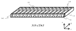
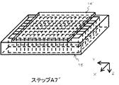
ステップA7では、得られたデュアルセルアレイの底面14´に底面反射材用樹脂18を形成する。図11に示すように、反射材用樹脂を事前に一定厚さで板状に硬化しておき、液状の反射材用樹脂でデュアルセルアレイの底面14´に接着して設けたり、液状の反射材用樹脂を一定厚さに塗布し、硬化して設けても良い。それにより、第1のシンチレータ及び第2のシンチレータのセルの周囲5面が反射材で覆われ、放射線検出器として受光素子と貼り合せて組み立てる際の受光面19のみが反射材用樹脂で覆われていないデュアルアレイ型のシンチレータアレイが完成する。 In Step A7, a bottom reflecting resin 18 is formed on the bottom surface 14 'of the obtained dual cell array. As shown in FIG. 11, the reflecting material resin is cured in a plate shape with a certain thickness in advance and is provided by adhering to the bottom surface 14 'of the dual cell array with a liquid reflecting material resin, or a liquid reflecting material. The coating resin may be applied to a certain thickness and cured. As a result, the five surfaces around the cells of the first scintillator and the second scintillator are covered with the reflecting material, and only the light receiving surface 19 when being assembled with the light receiving element as a radiation detector is covered with the resin for the reflecting material. A dual array scintillator array is completed.
これまでの説明において第2のシンチレータの基板に連結部21を形成したが、同様に第1のシンチレータの基板に連結部21を形成することも可能であり、第1のシンチレータの基板と第2のシンチレータの基板との加工性に応じて任意に選択しても良い。また、格子状溝付き積層基板の連結部21を支持プレートに固定して、格子状の溝に樹脂を充填し、硬化した後に連結部21を加工したが、格子状溝付き積層基板の連結部21の反対側の面を支持プレートに固定し、セル間寸法を維持しつつ、連結部21を加工してから、格子状の溝に樹脂を充填しても良い。
In the above description, the connecting
これまでに説明した方法を用いて、下記の条件でデュアルアレイ型のシンチレータアレイを作製した。第1のシンチレータとして、イットリウム‐ガドリニウム‐アルミニウム‐ガーネットのセラミックスシンチレータ焼結体からなる基板と、第2のシンチレータとして、GOSのセラミックスシンチレータ焼結体からなる基板を使用した。加工方法はダイヤの砥粒の砥石を使用し、積層工程においては基板上にバーコーターで塗布した反射材用樹脂を硬化させた後に、前記硬化した樹脂の上に液状の反射材用樹脂を薄く塗布して第2のシンチレータの基板を接着した。反射材用の樹脂として、白色の酸化チタン粉末を含有する熱硬化性エポキシ樹脂を用いた。以上の条件により得られたシンチレータアレイにおいて、デュアルアレイは十分に高い寸法精度を有していた。シンチレータセルを個々に並べていく方法に比べて、効率よくシンチレータセルを配列し、デュアルアレイ型のシンチレータアレイを作製できた。 Using the method described so far, a dual array type scintillator array was manufactured under the following conditions. A substrate made of a yttrium-gadolinium-aluminum-garnet ceramic scintillator sintered body was used as the first scintillator, and a substrate made of a GOS ceramic scintillator sintered body was used as the second scintillator. The processing method uses a grindstone of diamond abrasive grains, and in the laminating process, after the reflecting resin resin applied on the substrate with a bar coater is cured, the liquid reflecting resin resin is thinned on the cured resin. The substrate of the second scintillator was adhered by coating. A thermosetting epoxy resin containing white titanium oxide powder was used as the resin for the reflecting material. In the scintillator array obtained under the above conditions, the dual array has a sufficiently high dimensional accuracy. Compared to the method of arranging the scintillator cells individually, the scintillator cells were arranged efficiently and a dual array type scintillator array could be produced.
[2]第2の実施形態
デュアルセルの位置決めに支持プレートなどの位置決め手段を用いた第2の実施形態について図12のフローチャートを参照して説明する。まずステップA2までは第1の実施形態と同じ方法で行い、積層基板を得る。次にステップA3´において、第1の実施形態における連結部の代わりに、支持手段を用いてデュアルセルの位置を維持する。支持手段とは、溝加工工程及び樹脂充填工程などにおいて、格子状の溝の幅やピッチなどの寸法を維持しつつ、反射材用の樹脂を溝内に充填し、硬化してデュアルセルアレイ集合体を得られる方法であれば良い。
[2] Second Embodiment A second embodiment in which positioning means such as a support plate is used for positioning the dual cell will be described with reference to the flowchart of FIG. First, the process up to step A2 is performed by the same method as in the first embodiment, and a laminated substrate is obtained. Next, in Step A3 ′, the position of the dual cell is maintained using a support means instead of the connecting portion in the first embodiment. The support means is a dual cell array assembly that is filled with a resin for a reflecting material and cured in a groove processing step and a resin filling step while maintaining the dimensions and width of the lattice-like grooves. Any method can be used.
具体的には、例えば図13のようにガラス板などの平坦な支持プレート10上に粘着シート20などで支持する支持手段によって積層基板3の位置を維持したまま格子状の溝を加工し、さらに図14のように支持プレート10の周囲に型枠11を形成して樹脂を充填することが考えられる。もしくは、第1の実施形態のように、連結部21を残して格子状の溝を形成した後に、連結部とは反対側を支持プレート10に固定し、連結部21を除去することで、格子状の溝の幅やピッチなどの寸法を維持しても良い。得られたデュアルアレイ集合体は、ステップA5´において、支持プレート10を除去するだけで、図15のようにデュアルセルアレイを切断する準備ができる。ステップA6以降は第1の実施形態と同様である。この例では、支持プレート10の除去が容易に得られるようにしておくことで、第1の実施形態のように加工によって連結部21を除去する手間が省けるため、効率が良い。
Specifically, for example, as shown in FIG. 13, a grid-like groove is processed while maintaining the position of the laminated substrate 3 by a supporting means supported by a pressure-
[3]第3の実施形態
ステップA5以降の工程では、得られたシンチレータアレイを用いて放射線検出器を構成する際の構成に応じて、様々な形態をとりうる。第3の実施形態として、その一部の例を図16のフローチャートを参照して説明する。まず、他の実施形態などにより、ステップA5で連結部を除去したデュアルセルアレイ集合体を得る。
[3] Third Embodiment The steps after step A5 can take various forms depending on the configuration when the radiation detector is configured using the obtained scintillator array. As a third embodiment, a part of the example will be described with reference to a flowchart of FIG. First, according to another embodiment or the like, a dual cell array assembly from which the connecting portion is removed in step A5 is obtained.
ステップA7´として、図17に示すように、前記デュアルセルアレイ集合体の底面14´に反射材用樹脂を一定の厚さで形成する。このとき加工位置を確認するために、シンチレータアレイのセルとして使用しない領域の溝と、溝に充填した樹脂が見えるように、底面14´に反射材用樹脂を形成すると好ましい。続くステップA6´´では形成した反射材用樹脂ごと切断することで、複数のデュアルアレイ型のシンチレータアレイが得られるため効率が良い。
As step A7 ', as shown in FIG. 17, a resin for reflecting material is formed with a certain thickness on the bottom surface 14' of the dual cell array assembly. At this time, in order to confirm the processing position, it is preferable to form a resin for the reflecting material on the
他に第1の実施形態のステップA7を省略する方法として、ステップA6にてデュアルセルアレイを用いて放射線検出器に構成することもできる。例えば、事前にデュアルセルアレイの発光面と受光素子の受光面を対向させて貼りあわせた後に、反射材樹脂で形成した板の上面に、液状の反射材樹脂で接着し、配列する。これによりデュアルセルアレイを用いて、シンチレータアレイと放射線検出器を一度に構成できるため効率が良い。これらの工程は切り離したデュアルセルアレイの形態に応じて、適宜選択される。 As another method of omitting step A7 of the first embodiment, a radiation detector can be configured using a dual cell array in step A6. For example, after the light emitting surface of the dual cell array and the light receiving surface of the light receiving element are bonded to each other in advance, they are bonded and arranged on the upper surface of a plate formed of a reflective material resin with a liquid reflective material resin. As a result, the scintillator array and the radiation detector can be configured at a time using a dual cell array, which is efficient. These processes are appropriately selected according to the form of the separated dual cell array.
[4]第4の実施形態
第4の実施形態では、ステップA4において反射材用樹脂を格子状の溝に充填する際に、粘着シート20として熱剥離型の接着シートを使用する。熱剥離型の接着シートとは設定された温度まで加熱することによって、粘着力が低下し、剥離しやすくなる機能を有する接着シートで、特に反射材用樹脂を硬化した後に剥離するためには、接着材の中に発泡剤を含むものが好ましい。それにより、シンチレータアレイの製造方法全体としては、第2の実施形態で得られる効果に加え、樹脂を硬化した後に熱を加えるだけで剥離しやすくなる効果を得られる。
[4] Fourth Embodiment In the fourth embodiment, a heat-peelable adhesive sheet is used as the pressure-
ステップA3までは第2の実施形態と同じ方法で行い、図6のステップA4において、格子状溝付き積層基板5と接着する支持プレート10の面に熱剥離型の両面接着シート20を貼り付ける。このとき、少なくとも格子状溝付き積層基板5との接着面は熱剥離型の接着面となすが、さらに、支持プレート10との接着面も熱剥離型にすると、支持プレートを再利用できるため好ましい。
The process up to step A3 is performed in the same manner as in the second embodiment, and in step A4 of FIG. 6, the heat-peeling double-
尚、型枠11は熱剥離型の接着テープを格子状溝付き積層基板15を囲むように支持プレート10の上面に垂直に立てるように貼り付けても良いし、支持プレート10の側面にそれぞれ貼り付けて枠のようにしても良い。いずれの場合においても、反射材用樹脂に接触する側が、熱剥離型の接着面となるように配することで、樹脂硬化後の剥離が容易となるため、効率よくシンチレータアレイを形成できる。
The mold 11 may be affixed with a heat-peelable adhesive tape so as to stand vertically on the upper surface of the
本発明は、医療用CT装置の検出器又は手荷物検査用のCT装置の検出器に用いるX線吸収率が異なる2のシンチレータセルを用いたデュアルアレイ型のシンチレータアレイの製造に好適である。 The present invention is suitable for manufacturing a dual array type scintillator array using two scintillator cells having different X-ray absorption rates used for a detector of a medical CT apparatus or a detector of a CT apparatus for baggage inspection.
1・・・第1のシンチレータの基板
L1・・・第1のシンチレータの基板のY方向の辺の長さ
H1・・・第1のシンチレータの基板のZ方向の辺の高さ
W1・・・第1のシンチレータの基板のX方向の辺の幅
2・・・第2のシンチレータの基板
L2・・・第2のシンチレータの基板のY方向の辺の長さ
H2・・・第2のシンチレータの基板のZ方向の辺の高さ
W2・・・第2のシンチレータの基板のX方向の辺の幅
3・・・積層基板
4・・・樹脂層
5・・・格子状溝付き積層基板
6・・・回転砥石
7・・・X方向溝
8・・・回転砥石
9・・・Y方向溝
10・・・支持プレート
11・・・型枠
12・・・樹脂
13・・・デュアルセルアレイ集合体
14・・・底面
15・・・上面
16・・・回転砥石
17・・・背面反射材用樹脂
18・・・底面反射材用樹脂
19・・・受光面
20・・・粘着シート
21・・・連結部
DESCRIPTION OF
Claims (6)
第1のシンチレータ及び第2のシンチレータの基板を、反射材用樹脂層を介して積層し、積層基板を形成する積層工程と、
前記積層基板に格子状の溝を形成して、第1及び第2のシンチレータのセルが前記反射材用樹脂層を介して積層した形状を有するデュアルセルが林立した格子状溝付き積層基板を形成する溝加工工程と、
少なくとも前記格子状の溝に反射材用樹脂を充填し、デュアルセルアレイ集合体を形成する樹脂充填工程と、
前記格子状の溝のうち、一方向の反射材用樹脂を充填した溝に沿って切断し、デュアルセルアレイ集合体から、デュアルセルが配列したデュアルセルアレイに切り離す分離工程と、
を有することを特徴とするシンチレータアレイの製造方法。 A method of manufacturing a dual array type scintillator array,
A laminating step of laminating a substrate of the first scintillator and the second scintillator via a resin layer for a reflector, and forming a laminated substrate;
A lattice-shaped groove is formed in the multilayer substrate, and a lattice-shaped grooved multilayer substrate in which dual cells having a shape in which the cells of the first and second scintillators are stacked via the resin layer for the reflector is formed. Grooving process to perform,
A resin filling step of filling at least the lattice-shaped grooves with a resin for a reflecting material to form a dual cell array aggregate;
A separation step of cutting along a groove filled with a resin for a reflective material in one direction out of the lattice-shaped grooves, and separating from a dual cell array assembly into a dual cell array in which dual cells are arranged;
A method for manufacturing a scintillator array, comprising:
6. The method of manufacturing a scintillator array according to claim 5, wherein a heat-peelable adhesive sheet is used when adhering to the support plate in the resin filling step.
Priority Applications (1)
| Application Number | Priority Date | Filing Date | Title |
|---|---|---|---|
| JP2014068362A JP6358496B2 (en) | 2014-03-28 | 2014-03-28 | Manufacturing method of scintillator array |
Applications Claiming Priority (1)
| Application Number | Priority Date | Filing Date | Title |
|---|---|---|---|
| JP2014068362A JP6358496B2 (en) | 2014-03-28 | 2014-03-28 | Manufacturing method of scintillator array |
Publications (2)
| Publication Number | Publication Date |
|---|---|
| JP2015190853A true JP2015190853A (en) | 2015-11-02 |
| JP6358496B2 JP6358496B2 (en) | 2018-07-18 |
Family
ID=54425452
Family Applications (1)
| Application Number | Title | Priority Date | Filing Date |
|---|---|---|---|
| JP2014068362A Active JP6358496B2 (en) | 2014-03-28 | 2014-03-28 | Manufacturing method of scintillator array |
Country Status (1)
| Country | Link |
|---|---|
| JP (1) | JP6358496B2 (en) |
Cited By (3)
| Publication number | Priority date | Publication date | Assignee | Title |
|---|---|---|---|---|
| WO2019019041A1 (en) | 2017-07-26 | 2019-01-31 | Shenzhen Xpectvision Technology Co., Ltd. | Methods of making and using an x-ray detector |
| CN109459781A (en) * | 2018-10-27 | 2019-03-12 | 惠磊光电科技(上海)有限公司 | A kind of processing technology of scintillation array |
| CN109991648A (en) * | 2017-12-29 | 2019-07-09 | 北京一轻研究院 | A method of making scintillator arrays |
Citations (13)
| Publication number | Priority date | Publication date | Assignee | Title |
|---|---|---|---|---|
| JPH01117583U (en) * | 1988-02-03 | 1989-08-08 | ||
| JPH1184013A (en) * | 1997-09-02 | 1999-03-26 | Shimadzu Corp | Radiation detector |
| JP2002202375A (en) * | 2000-11-03 | 2002-07-19 | Siemens Ag | Method of manufacturing detector array for detecting electromagnetic waves and detector array |
| JP2002311142A (en) * | 2001-04-18 | 2002-10-23 | Toshiba Corp | Method of manufacturing x-ray solid-state detector and x-ray ct apparatus |
| JP2005201891A (en) * | 2003-12-11 | 2005-07-28 | Ge Medical Systems Global Technology Co Llc | Multilayer reflector for detector of ct |
| US7157014B1 (en) * | 2001-10-05 | 2007-01-02 | Cit Pet Systems, Inc. | Method for producing a high resolution detector array |
| JP2009524015A (en) * | 2006-01-16 | 2009-06-25 | コーニンクレッカ フィリップス エレクトロニクス エヌ ヴィ | Scintillation element, scintillation array and method for producing scintillation element and scintillation array |
| US20100127180A1 (en) * | 2008-11-24 | 2010-05-27 | Cmt Medical Technologies Ltd. | Scintillator array and a method of constructing the same |
| WO2012147747A1 (en) * | 2011-04-25 | 2012-11-01 | 日立金属株式会社 | Method for producing scintillator array |
| WO2013146167A1 (en) * | 2012-03-30 | 2013-10-03 | 日立金属株式会社 | Scintillator dual array manufacturing method |
| JP2013228355A (en) * | 2012-03-30 | 2013-11-07 | Hitachi Metals Ltd | Method for manufacturing scintillator array and radiation detector |
| JP2014085222A (en) * | 2012-10-24 | 2014-05-12 | Hitachi Metals Ltd | Method for manufacturing scintillator arrays |
| JP2014085223A (en) * | 2012-10-24 | 2014-05-12 | Hitachi Metals Ltd | Method for manufacturing scintillator array |
-
2014
- 2014-03-28 JP JP2014068362A patent/JP6358496B2/en active Active
Patent Citations (13)
| Publication number | Priority date | Publication date | Assignee | Title |
|---|---|---|---|---|
| JPH01117583U (en) * | 1988-02-03 | 1989-08-08 | ||
| JPH1184013A (en) * | 1997-09-02 | 1999-03-26 | Shimadzu Corp | Radiation detector |
| JP2002202375A (en) * | 2000-11-03 | 2002-07-19 | Siemens Ag | Method of manufacturing detector array for detecting electromagnetic waves and detector array |
| JP2002311142A (en) * | 2001-04-18 | 2002-10-23 | Toshiba Corp | Method of manufacturing x-ray solid-state detector and x-ray ct apparatus |
| US7157014B1 (en) * | 2001-10-05 | 2007-01-02 | Cit Pet Systems, Inc. | Method for producing a high resolution detector array |
| JP2005201891A (en) * | 2003-12-11 | 2005-07-28 | Ge Medical Systems Global Technology Co Llc | Multilayer reflector for detector of ct |
| JP2009524015A (en) * | 2006-01-16 | 2009-06-25 | コーニンクレッカ フィリップス エレクトロニクス エヌ ヴィ | Scintillation element, scintillation array and method for producing scintillation element and scintillation array |
| US20100127180A1 (en) * | 2008-11-24 | 2010-05-27 | Cmt Medical Technologies Ltd. | Scintillator array and a method of constructing the same |
| WO2012147747A1 (en) * | 2011-04-25 | 2012-11-01 | 日立金属株式会社 | Method for producing scintillator array |
| WO2013146167A1 (en) * | 2012-03-30 | 2013-10-03 | 日立金属株式会社 | Scintillator dual array manufacturing method |
| JP2013228355A (en) * | 2012-03-30 | 2013-11-07 | Hitachi Metals Ltd | Method for manufacturing scintillator array and radiation detector |
| JP2014085222A (en) * | 2012-10-24 | 2014-05-12 | Hitachi Metals Ltd | Method for manufacturing scintillator arrays |
| JP2014085223A (en) * | 2012-10-24 | 2014-05-12 | Hitachi Metals Ltd | Method for manufacturing scintillator array |
Cited By (8)
| Publication number | Priority date | Publication date | Assignee | Title |
|---|---|---|---|---|
| WO2019019041A1 (en) | 2017-07-26 | 2019-01-31 | Shenzhen Xpectvision Technology Co., Ltd. | Methods of making and using an x-ray detector |
| CN110914714A (en) * | 2017-07-26 | 2020-03-24 | 深圳帧观德芯科技有限公司 | Methods of making and using X-ray detectors |
| EP3658964A4 (en) * | 2017-07-26 | 2021-01-13 | Shenzhen Xpectvision Technology Co., Ltd. | METHOD OF MANUFACTURING AND USING AN X-RAY DETECTOR |
| US11156726B2 (en) | 2017-07-26 | 2021-10-26 | Shenzhen Xpectvision Technology Co., Ltd. | Methods of making and using an x-ray detector |
| TWI804502B (en) * | 2017-07-26 | 2023-06-11 | 中國大陸商深圳幀觀德芯科技有限公司 | Methods of making an x-ray detector |
| CN110914714B (en) * | 2017-07-26 | 2024-02-27 | 深圳帧观德芯科技有限公司 | Method of manufacturing and using an X-ray detector |
| CN109991648A (en) * | 2017-12-29 | 2019-07-09 | 北京一轻研究院 | A method of making scintillator arrays |
| CN109459781A (en) * | 2018-10-27 | 2019-03-12 | 惠磊光电科技(上海)有限公司 | A kind of processing technology of scintillation array |
Also Published As
| Publication number | Publication date |
|---|---|
| JP6358496B2 (en) | 2018-07-18 |
Similar Documents
| Publication | Publication Date | Title |
|---|---|---|
| JP5935919B2 (en) | Manufacturing method of scintillator array | |
| CN103443652B (en) | spectral imaging detector | |
| JP5854128B2 (en) | Manufacturing method of scintillator dual array | |
| JP6358496B2 (en) | Manufacturing method of scintillator array | |
| JP6115570B2 (en) | Manufacturing method of radiation detector | |
| JP2008510131A (en) | Arrangement of scintillator and anti-scatter grid | |
| JP6052595B2 (en) | Manufacturing method of scintillator array | |
| US20110056618A1 (en) | Method of manufacturing radiation detector | |
| JP5541413B2 (en) | Manufacturing method of scintillator array | |
| US9400334B2 (en) | Scintillator array, a scintillator, a radiation detection apparatus including the scintillator array or scintillator, and processes of forming the same | |
| JP2002311142A (en) | Method of manufacturing x-ray solid-state detector and x-ray ct apparatus | |
| JP2004184163A (en) | Radiation detector and medical image diagnostic device | |
| JP6233730B2 (en) | Manufacturing method of scintillator array | |
| JP6052594B2 (en) | Manufacturing method of scintillator array | |
| US20110024023A1 (en) | Method of manufacturing light guide and method of manufacturing a radiation detector | |
| JP2001249180A (en) | Manufacturing method of two-dimensional array type radiation detector | |
| JP2019168350A (en) | Scintillator array and method for manufacturing the same | |
| JP2016223845A (en) | Radiation detector, radiation detection device, and method for manufacturing radiation detector | |
| JP5997892B2 (en) | X-ray detector, X-ray CT apparatus, and method of manufacturing X-ray detector |
Legal Events
| Date | Code | Title | Description |
|---|---|---|---|
| A621 | Written request for application examination |
Free format text: JAPANESE INTERMEDIATE CODE: A621 Effective date: 20170213 |
|
| A977 | Report on retrieval |
Free format text: JAPANESE INTERMEDIATE CODE: A971007 Effective date: 20171011 |
|
| A131 | Notification of reasons for refusal |
Free format text: JAPANESE INTERMEDIATE CODE: A131 Effective date: 20171102 |
|
| A521 | Request for written amendment filed |
Free format text: JAPANESE INTERMEDIATE CODE: A523 Effective date: 20171214 |
|
| TRDD | Decision of grant or rejection written | ||
| A01 | Written decision to grant a patent or to grant a registration (utility model) |
Free format text: JAPANESE INTERMEDIATE CODE: A01 Effective date: 20180525 |
|
| A61 | First payment of annual fees (during grant procedure) |
Free format text: JAPANESE INTERMEDIATE CODE: A61 Effective date: 20180607 |
|
| R150 | Certificate of patent or registration of utility model |
Ref document number: 6358496 Country of ref document: JP Free format text: JAPANESE INTERMEDIATE CODE: R150 |
|
| S531 | Written request for registration of change of domicile |
Free format text: JAPANESE INTERMEDIATE CODE: R313531 |
|
| S533 | Written request for registration of change of name |
Free format text: JAPANESE INTERMEDIATE CODE: R313533 |
|
| R350 | Written notification of registration of transfer |
Free format text: JAPANESE INTERMEDIATE CODE: R350 |