JP2015114663A - Liquid crystal display device and driving method thereof - Google Patents
Liquid crystal display device and driving method thereof Download PDFInfo
- Publication number
- JP2015114663A JP2015114663A JP2014226372A JP2014226372A JP2015114663A JP 2015114663 A JP2015114663 A JP 2015114663A JP 2014226372 A JP2014226372 A JP 2014226372A JP 2014226372 A JP2014226372 A JP 2014226372A JP 2015114663 A JP2015114663 A JP 2015114663A
- Authority
- JP
- Japan
- Prior art keywords
- data
- sub
- liquid crystal
- subpixels
- voltage
- Prior art date
- Legal status (The legal status is an assumption and is not a legal conclusion. Google has not performed a legal analysis and makes no representation as to the accuracy of the status listed.)
- Granted
Links
Images


Classifications
-
- G—PHYSICS
- G02—OPTICS
- G02F—OPTICAL DEVICES OR ARRANGEMENTS FOR THE CONTROL OF LIGHT BY MODIFICATION OF THE OPTICAL PROPERTIES OF THE MEDIA OF THE ELEMENTS INVOLVED THEREIN; NON-LINEAR OPTICS; FREQUENCY-CHANGING OF LIGHT; OPTICAL LOGIC ELEMENTS; OPTICAL ANALOGUE/DIGITAL CONVERTERS
- G02F1/00—Devices or arrangements for the control of the intensity, colour, phase, polarisation or direction of light arriving from an independent light source, e.g. switching, gating or modulating; Non-linear optics
- G02F1/01—Devices or arrangements for the control of the intensity, colour, phase, polarisation or direction of light arriving from an independent light source, e.g. switching, gating or modulating; Non-linear optics for the control of the intensity, phase, polarisation or colour
- G02F1/13—Devices or arrangements for the control of the intensity, colour, phase, polarisation or direction of light arriving from an independent light source, e.g. switching, gating or modulating; Non-linear optics for the control of the intensity, phase, polarisation or colour based on liquid crystals, e.g. single liquid crystal display cells
- G02F1/133—Constructional arrangements; Operation of liquid crystal cells; Circuit arrangements
-
- G—PHYSICS
- G09—EDUCATION; CRYPTOGRAPHY; DISPLAY; ADVERTISING; SEALS
- G09G—ARRANGEMENTS OR CIRCUITS FOR CONTROL OF INDICATING DEVICES USING STATIC MEANS TO PRESENT VARIABLE INFORMATION
- G09G3/00—Control arrangements or circuits, of interest only in connection with visual indicators other than cathode-ray tubes
- G09G3/20—Control arrangements or circuits, of interest only in connection with visual indicators other than cathode-ray tubes for presentation of an assembly of a number of characters, e.g. a page, by composing the assembly by combination of individual elements arranged in a matrix no fixed position being assigned to or needed to be assigned to the individual characters or partial characters
- G09G3/34—Control arrangements or circuits, of interest only in connection with visual indicators other than cathode-ray tubes for presentation of an assembly of a number of characters, e.g. a page, by composing the assembly by combination of individual elements arranged in a matrix no fixed position being assigned to or needed to be assigned to the individual characters or partial characters by control of light from an independent source
- G09G3/36—Control arrangements or circuits, of interest only in connection with visual indicators other than cathode-ray tubes for presentation of an assembly of a number of characters, e.g. a page, by composing the assembly by combination of individual elements arranged in a matrix no fixed position being assigned to or needed to be assigned to the individual characters or partial characters by control of light from an independent source using liquid crystals
- G09G3/3611—Control of matrices with row and column drivers
- G09G3/3614—Control of polarity reversal in general
-
- G—PHYSICS
- G02—OPTICS
- G02F—OPTICAL DEVICES OR ARRANGEMENTS FOR THE CONTROL OF LIGHT BY MODIFICATION OF THE OPTICAL PROPERTIES OF THE MEDIA OF THE ELEMENTS INVOLVED THEREIN; NON-LINEAR OPTICS; FREQUENCY-CHANGING OF LIGHT; OPTICAL LOGIC ELEMENTS; OPTICAL ANALOGUE/DIGITAL CONVERTERS
- G02F1/00—Devices or arrangements for the control of the intensity, colour, phase, polarisation or direction of light arriving from an independent light source, e.g. switching, gating or modulating; Non-linear optics
- G02F1/01—Devices or arrangements for the control of the intensity, colour, phase, polarisation or direction of light arriving from an independent light source, e.g. switching, gating or modulating; Non-linear optics for the control of the intensity, phase, polarisation or colour
- G02F1/13—Devices or arrangements for the control of the intensity, colour, phase, polarisation or direction of light arriving from an independent light source, e.g. switching, gating or modulating; Non-linear optics for the control of the intensity, phase, polarisation or colour based on liquid crystals, e.g. single liquid crystal display cells
- G02F1/133—Constructional arrangements; Operation of liquid crystal cells; Circuit arrangements
- G02F1/136—Liquid crystal cells structurally associated with a semi-conducting layer or substrate, e.g. cells forming part of an integrated circuit
- G02F1/1362—Active matrix addressed cells
-
- G—PHYSICS
- G09—EDUCATION; CRYPTOGRAPHY; DISPLAY; ADVERTISING; SEALS
- G09G—ARRANGEMENTS OR CIRCUITS FOR CONTROL OF INDICATING DEVICES USING STATIC MEANS TO PRESENT VARIABLE INFORMATION
- G09G3/00—Control arrangements or circuits, of interest only in connection with visual indicators other than cathode-ray tubes
- G09G3/20—Control arrangements or circuits, of interest only in connection with visual indicators other than cathode-ray tubes for presentation of an assembly of a number of characters, e.g. a page, by composing the assembly by combination of individual elements arranged in a matrix no fixed position being assigned to or needed to be assigned to the individual characters or partial characters
- G09G3/34—Control arrangements or circuits, of interest only in connection with visual indicators other than cathode-ray tubes for presentation of an assembly of a number of characters, e.g. a page, by composing the assembly by combination of individual elements arranged in a matrix no fixed position being assigned to or needed to be assigned to the individual characters or partial characters by control of light from an independent source
- G09G3/36—Control arrangements or circuits, of interest only in connection with visual indicators other than cathode-ray tubes for presentation of an assembly of a number of characters, e.g. a page, by composing the assembly by combination of individual elements arranged in a matrix no fixed position being assigned to or needed to be assigned to the individual characters or partial characters by control of light from an independent source using liquid crystals
-
- G—PHYSICS
- G09—EDUCATION; CRYPTOGRAPHY; DISPLAY; ADVERTISING; SEALS
- G09G—ARRANGEMENTS OR CIRCUITS FOR CONTROL OF INDICATING DEVICES USING STATIC MEANS TO PRESENT VARIABLE INFORMATION
- G09G2310/00—Command of the display device
- G09G2310/06—Details of flat display driving waveforms
- G09G2310/065—Waveforms comprising zero voltage phase or pause
-
- G—PHYSICS
- G09—EDUCATION; CRYPTOGRAPHY; DISPLAY; ADVERTISING; SEALS
- G09G—ARRANGEMENTS OR CIRCUITS FOR CONTROL OF INDICATING DEVICES USING STATIC MEANS TO PRESENT VARIABLE INFORMATION
- G09G2320/00—Control of display operating conditions
- G09G2320/02—Improving the quality of display appearance
- G09G2320/0204—Compensation of DC component across the pixels in flat panels
-
- G—PHYSICS
- G09—EDUCATION; CRYPTOGRAPHY; DISPLAY; ADVERTISING; SEALS
- G09G—ARRANGEMENTS OR CIRCUITS FOR CONTROL OF INDICATING DEVICES USING STATIC MEANS TO PRESENT VARIABLE INFORMATION
- G09G3/00—Control arrangements or circuits, of interest only in connection with visual indicators other than cathode-ray tubes
- G09G3/20—Control arrangements or circuits, of interest only in connection with visual indicators other than cathode-ray tubes for presentation of an assembly of a number of characters, e.g. a page, by composing the assembly by combination of individual elements arranged in a matrix no fixed position being assigned to or needed to be assigned to the individual characters or partial characters
- G09G3/34—Control arrangements or circuits, of interest only in connection with visual indicators other than cathode-ray tubes for presentation of an assembly of a number of characters, e.g. a page, by composing the assembly by combination of individual elements arranged in a matrix no fixed position being assigned to or needed to be assigned to the individual characters or partial characters by control of light from an independent source
- G09G3/36—Control arrangements or circuits, of interest only in connection with visual indicators other than cathode-ray tubes for presentation of an assembly of a number of characters, e.g. a page, by composing the assembly by combination of individual elements arranged in a matrix no fixed position being assigned to or needed to be assigned to the individual characters or partial characters by control of light from an independent source using liquid crystals
- G09G3/3607—Control arrangements or circuits, of interest only in connection with visual indicators other than cathode-ray tubes for presentation of an assembly of a number of characters, e.g. a page, by composing the assembly by combination of individual elements arranged in a matrix no fixed position being assigned to or needed to be assigned to the individual characters or partial characters by control of light from an independent source using liquid crystals for displaying colours or for displaying grey scales with a specific pixel layout, e.g. using sub-pixels
Landscapes
- Physics & Mathematics (AREA)
- Engineering & Computer Science (AREA)
- General Physics & Mathematics (AREA)
- Crystallography & Structural Chemistry (AREA)
- Chemical & Material Sciences (AREA)
- Theoretical Computer Science (AREA)
- Computer Hardware Design (AREA)
- Nonlinear Science (AREA)
- Mathematical Physics (AREA)
- Optics & Photonics (AREA)
- Microelectronics & Electronic Packaging (AREA)
- Control Of Indicators Other Than Cathode Ray Tubes (AREA)
- Liquid Crystal (AREA)
- Liquid Crystal Display Device Control (AREA)
Abstract
Description
本発明は液晶表示装置及びその駆動方法に関するものである。 The present invention relates to a liquid crystal display device and a driving method thereof.
液晶表示装置は現在最も広く使用されている平板表示装置の1つであって、液晶表示パネルの画素電極と共通電極に互いに異なる電位を印加して電場を形成することによって液晶分子の配列を変更させ、これによって透光率を調節して画像を表現する装置である。 The liquid crystal display device is one of the most widely used flat panel display devices, and the arrangement of liquid crystal molecules is changed by applying different potentials to the pixel electrode and the common electrode of the liquid crystal display panel to form an electric field. Thus, the device expresses an image by adjusting the transmissivity.
液晶物質に同一方向の電場を続けて印加すると劣化が起こるため、これを防止するために共通電極に印加される電圧に対する画素電極に印加される電圧の極性を反転させる駆動を行なうことが一般的である。しかし、偶数個の副画素からなる画素を有する液晶表示装置で反転駆動する場合、データ電圧の極性偏り現象が起こることがある。 Deterioration occurs when an electric field in the same direction is continuously applied to the liquid crystal material. Therefore, in order to prevent this, it is common to perform driving that reverses the polarity of the voltage applied to the pixel electrode with respect to the voltage applied to the common electrode. It is. However, when the liquid crystal display device having a pixel composed of an even number of sub-pixels is driven in an inverted manner, a data voltage polarity bias phenomenon may occur.
本発明は、表示品質に優れた液晶表示装置及びその駆動方法を提供することを目的とする。 An object of the present invention is to provide a liquid crystal display device excellent in display quality and a driving method thereof.
本発明はまた、偶数個の副画素からなる画素を有する液晶表示装置でデータ電圧の極性偏りが起こらない極性配置を提供することを目的とする。 Another object of the present invention is to provide a polarity arrangement in which a polarity deviation of a data voltage does not occur in a liquid crystal display device having pixels composed of an even number of subpixels.
このような課題を解決するために本発明の一実施形態による液晶表示装置は、行方向に配列された複数のゲートラインと、列方向に配列された複数のデータラインと、前記ゲートライン及び前記データラインにそれぞれ接続され、行に沿って連続して配列されている8つの副画素を含む基本単位が行列方向に配列されている複数の副画素とを含み、前記基本単位で、行に沿って一番目の副画素から四番目の副画素までは隣接副画素に印加される電圧の極性が反対であり、五番目の副画素から八番目の副画素までも隣接副画素に印加される電圧の極性が反対であるが、前記四番目の副画素と前記五番目の副画素に印加される電圧の極性は同一である。 In order to solve such a problem, a liquid crystal display according to an embodiment of the present invention includes a plurality of gate lines arranged in a row direction, a plurality of data lines arranged in a column direction, the gate lines, and the gate lines. A plurality of sub-pixels each including a plurality of sub-pixels arranged in a matrix direction, each of which is connected to the data line and includes eight sub-pixels arranged in succession along the row. From the first subpixel to the fourth subpixel, the polarity of the voltage applied to the adjacent subpixel is opposite, and from the fifth subpixel to the eighth subpixel, the voltage applied to the adjacent subpixel. However, the polarities of the voltages applied to the fourth subpixel and the fifth subpixel are the same.
前記液晶表示装置で、前記複数の副画素に印加される電圧の極性が列方向に同一であってもよい。 In the liquid crystal display device, polarities of voltages applied to the plurality of sub-pixels may be the same in the column direction.
前記液晶表示装置で、列方向に3つの副画素ごとに、印加される電圧の極性が反対であってもよい。 In the liquid crystal display device, the polarity of the applied voltage may be opposite for every three subpixels in the column direction.
それぞれのデータラインは自分の左側及び右側のうちのいずれか一方に位置した副画素にのみ接続されていてもよい。 Each data line may be connected only to the sub-pixel located on either the left side or the right side of itself.
前記液晶表示装置で、偶数個の副画素が1つの画素を成しても良く、例えば4つの副画素が1つの画素を成してもよい。 In the liquid crystal display device, an even number of subpixels may form one pixel, for example, four subpixels may form one pixel.
前記液晶表示装置で、特定の順序で配列された4つの色をそれぞれ表示する4つの副画素が行列方向に繰り返されてもよい。 In the liquid crystal display device, four sub-pixels that respectively display four colors arranged in a specific order may be repeated in the matrix direction.
本発明の他の一実施形態による液晶表示装置は、行方向に配列された複数のゲートラインと、列方向に配列された複数のデータラインと、前記ゲートライン及び前記データラインにそれぞれ接続され、行に沿って連続して配列されている4つの副画素を含む基本単位が行列方向に配列されている複数の副画素とを含む。前記基本単位で、行に沿って2つの副画素ごとに、印加される電圧の極性が反対である。また、列に沿って隣接の2つの列のうちの一列にある副画素は印加される電圧の極性が同一であり、他の一列にある副画素は隣接副画素間で印加される電圧の極性が反対である。 A liquid crystal display according to another exemplary embodiment of the present invention includes a plurality of gate lines arranged in a row direction, a plurality of data lines arranged in a column direction, and the gate lines and the data lines, respectively. A basic unit including four subpixels arranged continuously along a row includes a plurality of subpixels arranged in a matrix direction. In the basic unit, the polarity of the applied voltage is opposite for every two sub-pixels along the row. In addition, the subpixels in one of the two adjacent columns along the column have the same polarity of the applied voltage, and the subpixels in the other column have the polarity of the voltage applied between the adjacent subpixels. Is the opposite.
それぞれのデータラインは自分の左側及び右側に位置した副画素に列方向に1つずつ交互に接続されていてもよい。 Each data line may be alternately connected to the subpixels located on the left side and the right side of the data line one by one in the column direction.
本発明のまた他の一実施形態による液晶表示装置は、行方向に配列された複数のゲートラインと、列方向に配列された複数のデータラインと、前記ゲートライン及び前記データラインにそれぞれ接続され、行に沿って連続して配列されている8つの副画素を含む基本単位が行列方向に配列されている複数の副画素とを含む。前記基本単位で、行方向に第1乃至第4副画素は隣接副画素に印加される電圧の極性が反対であり、第5乃至第8副画素も隣接副画素に印加される電圧の極性が反対であるが、前記第4副画素と前記第5副画素は印加される電圧の極性が同一である。また、列方向に第1乃至第3列及び第5乃至第7列の副画素は3つの副画素を繰り返し単位にし、各繰り返し単位で隣接副画素に印加される電圧の極性が反対であり、第4列及び第8列の副画素は3つの副画素ごとに極性が反対である。 A liquid crystal display according to another embodiment of the present invention includes a plurality of gate lines arranged in a row direction, a plurality of data lines arranged in a column direction, and the gate lines and the data lines, respectively. The basic unit including eight subpixels arranged continuously along a row includes a plurality of subpixels arranged in the matrix direction. In the basic unit, in the row direction, the first to fourth subpixels have opposite polarities of voltages applied to adjacent subpixels, and the fifth to eighth subpixels also have polarities of voltages applied to adjacent subpixels. On the contrary, the fourth subpixel and the fifth subpixel have the same polarity of applied voltage. The subpixels in the first to third columns and the fifth to seventh columns in the column direction have three subpixels as a repeating unit, and the polarity of the voltage applied to the adjacent subpixel in each repeating unit is opposite, The subpixels in the fourth and eighth columns have opposite polarities for every three subpixels.
それぞれのデータラインは自分の左側及び右側に位置した副画素に列方向に1つずつ交互に接続されていてもよい。 Each data line may be alternately connected to the subpixels located on the left side and the right side of the data line one by one in the column direction.
本発明のまた他の一実施形態による液晶表示装置は、行方向に配列された複数のゲートラインと、列方向に配列された複数のデータラインと、前記ゲートライン及び前記データラインにそれぞれ接続され、行に沿って連続して配列されている8つの副画素を含む基本単位が行列方向に配列されている複数の副画素とを含む。前記基本単位で、行方向に第1乃至第4副画素は印加される電圧の極性が同一であり、第5乃至第8副画素は前記第1乃至第4副画素と印加される電圧の極性が反対である。また、列方向に第1乃至第3列及び第5乃至第7列の副画素は3つの副画素ごとに印加される電圧の極性が反対であり、第4列及び第8列の副画素は3つの副画素を繰り返し単位にし、各繰り返し単位で隣接副画素に印加される電圧の極性が反対である。 A liquid crystal display according to another embodiment of the present invention includes a plurality of gate lines arranged in a row direction, a plurality of data lines arranged in a column direction, and the gate lines and the data lines, respectively. The basic unit including eight subpixels arranged continuously along a row includes a plurality of subpixels arranged in the matrix direction. In the basic unit, the polarity of the applied voltage is the same in the first to fourth subpixels in the row direction, and the polarity of the applied voltage is the same as that of the first to fourth subpixels in the fifth to eighth subpixels. Is the opposite. In addition, the subpixels in the first to third columns and the fifth to seventh columns in the column direction have opposite polarities of voltages applied to the three subpixels, and the subpixels in the fourth column and the eighth column are Three subpixels are used as a repeating unit, and the polarity of the voltage applied to the adjacent subpixel in each repeating unit is opposite.
それぞれのデータラインは自分の左側及び右側に位置した副画素に列方向に1つずつ交互に接続されていてもよい。 Each data line may be alternately connected to the subpixels located on the left side and the right side of the data line one by one in the column direction.
本発明のまた他の一実施形態による液晶表示装置は、行方向に配列された複数のゲートラインと、列方向に配列された複数のデータラインと、前記ゲートライン及び前記データラインにそれぞれ接続され、行に沿って連続して配列されている4つの副画素を含む基本単位が行列方向に配列されている複数の副画素とを含む。前記基本単位で、行に沿って2つの副画素ごとに、印加される電圧の極性が反対である。また、列方向に隣接の2つの列のうちの一列にある副画素は印加される電圧の極性が同一であり、他の一列にある副画素は2つの副画素ごとに印加される電圧の極性が反対である。 A liquid crystal display according to another embodiment of the present invention includes a plurality of gate lines arranged in a row direction, a plurality of data lines arranged in a column direction, and the gate lines and the data lines, respectively. The basic unit including four sub-pixels arranged continuously along the row includes a plurality of sub-pixels arranged in the matrix direction. In the basic unit, the polarity of the applied voltage is opposite for every two sub-pixels along the row. In addition, the subpixels in one of the two columns adjacent in the column direction have the same polarity of the applied voltage, and the subpixels in the other column have the polarity of the voltage applied to every two subpixels. Is the opposite.
それぞれのデータラインは自分の左側及び右側に位置した副画素に列方向に2つずつ交互に接続されていてもよい。 Each data line may be alternately connected to the subpixels located on the left side and the right side of the data line by two in the column direction.
本発明のまた他の一実施形態による液晶表示装置は、行方向に配列された複数のゲートラインと、列方向に配列された複数のデータラインと、前記ゲートライン及び前記データラインにそれぞれ接続され、行に沿って連続して配列されている6つの副画素を含む基本単位が行列方向に配列されている複数の副画素とを含む。前記基本単位で、行に沿って3つの副画素ごとに印加される電圧の極性が反対である。 A liquid crystal display according to another embodiment of the present invention includes a plurality of gate lines arranged in a row direction, a plurality of data lines arranged in a column direction, and the gate lines and the data lines, respectively. The basic unit including six subpixels arranged continuously along a row includes a plurality of subpixels arranged in a matrix direction. In the basic unit, the polarity of the voltage applied to every three subpixels along the row is opposite.
それぞれのデータラインは自分の左側及び右側に位置した副画素に列方向に2つずつ交互に接続されていてもよい。 Each data line may be alternately connected to the subpixels located on the left side and the right side of the data line by two in the column direction.
前記液晶表示装置で、列方向に4つの副画素ごとに印加される電圧の極性が反対であってもよい。 In the liquid crystal display device, polarities of voltages applied to every four subpixels in the column direction may be opposite.
前記液晶表示装置で、列方向に隣接の3つの列のうちの 2つの列にある副画素はそれぞれの列で印加される電圧の極性が同一であり、他の一列にある副画素は2つの副画素ごとに印加される電圧の極性が反対であってもよい。 In the liquid crystal display device, the subpixels in two of the three columns adjacent in the column direction have the same polarity of the voltage applied in each column, and the subpixels in the other column have two subpixels. The polarity of the voltage applied to each subpixel may be opposite.
本発明の他の一側面において、行方向に配列されたゲートライン及び列方向に配列されたデータラインにそれぞれ接続され、行列方向に配列されている複数の副画素を含む液晶表示装置を駆動する方法が提供される。前記方法で、データ駆動部は第1乃至第4副画素列に接続されたデータラインには隣接ゲートライン間に極性が反対であるデータ電圧を印加し、第5乃至第8副画素列に接続されたデータラインも隣接ゲートライン間に極性が反対であるデータ電圧を印加するが、前記第4副画素列に接続されたデータラインと前記第5副画素列に接続されたデータラインには同一な極性のデータ電圧を印加する。 In another aspect of the present invention, a liquid crystal display device including a plurality of sub-pixels connected to gate lines arranged in a row direction and data lines arranged in a column direction and arranged in a matrix direction is driven. A method is provided. In this method, the data driver applies data voltages having opposite polarities between adjacent gate lines to the data lines connected to the first to fourth subpixel columns, and connects to the fifth to eighth subpixel columns. A data voltage having the opposite polarity is applied between adjacent gate lines, but the data line connected to the fourth subpixel column and the data line connected to the fifth subpixel column are the same. Apply a data voltage of the correct polarity.
それぞれのデータラインは自分の左側及び右側のうちのいずれか一方に位置した副画素にのみ接続されていてもよい。 Each data line may be connected only to the sub-pixel located on either the left side or the right side of itself.
前記データ駆動部は1フレーム内でそれぞれのデータラインに同一な極性のデータ電圧を印加してもよい。 The data driver may apply a data voltage having the same polarity to each data line within one frame.
前記データ駆動部はそれぞれのデータラインに3つのゲートラインごとに極性が反対であるデータ電圧を印加してもよい。 The data driver may apply to each data line a data voltage having the opposite polarity for every three gate lines.
本発明による極性配置による場合、データ電圧の極性偏りが起こらないので、共通電圧のリップル(ripple)現象が起こらないのは当然のことであり、1フレームで、またはフレーム間に輝度差が発生しない。したがって、液晶表示装置の表示品質を向上させることができる。 In the case of the polarity arrangement according to the present invention, since the polarity deviation of the data voltage does not occur, it is natural that the ripple phenomenon of the common voltage does not occur, and there is no luminance difference in one frame or between frames. . Therefore, the display quality of the liquid crystal display device can be improved.
添付した図面を参照して、本発明の実施形態について本発明の属する技術分野における通常の知識を有する者が容易に実施することができるように詳しく説明する。しかし、本発明は様々な形態に実現でき、ここで説明する実施形態に限定されない。 The embodiments of the present invention will be described in detail with reference to the accompanying drawings so that those skilled in the art to which the present invention pertains can easily carry out the embodiments. However, the present invention can be realized in various forms and is not limited to the embodiments described here.
本発明の実施形態による液晶表示装置及びその駆動方法について図面を参照して詳細に説明する。 A liquid crystal display device and a driving method thereof according to an embodiment of the present invention will be described in detail with reference to the drawings.
まず、図1及び図2を参照して本発明の一実施形態による液晶表示装置及びその駆動方法について説明する。 First, a liquid crystal display device and a driving method thereof according to an embodiment of the present invention will be described with reference to FIGS.
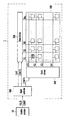
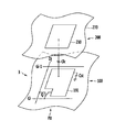
図1は本発明の一実施形態による液晶表示装置のブロック図であり、図2は本発明の一実施形態による液晶表示装置で一副画素の等価回路図である。 FIG. 1 is a block diagram of a liquid crystal display device according to an embodiment of the present invention, and FIG. 2 is an equivalent circuit diagram of one subpixel in the liquid crystal display device according to an embodiment of the present invention.
図1に示されているように、液晶表示装置1は映像を表示する液晶表示パネル300、ゲート駆動部400、データ駆動部500、及び信号制御部600を含む。また、図1には液晶表示装置1の外部に位置するグラフィック処理部10が示されている。
As shown in FIG. 1, the liquid
グラフィック処理部10は映像信号R、G、Bと制御信号CONTを液晶表示装置1の信号制御部600に提供する。前記制御信号CONTは水平同期信号Hsync、垂直同期信号Vsync、クロック信号CLK、データイネーブル信号DEなどを含む。映像信号R、G、Bと制御信号CONTは例えばLVDS(low voltage differential signaling)方式で信号制御部600に転送されてもよい。
The
液晶表示パネル300は互いに対向する下部及び上部パネル100、200とその間に介された液晶層3を含む。液晶表示パネル300は複数のゲートラインG1−Gnと複数のデータラインD1−Dmを含む。複数のゲートラインG1−Gnはほぼ横(行)方向に延長されており、複数のデータラインD1−Dmは複数のゲートラインG1−Gnと絶縁されて交差しながらほぼ縦(列)方向に延長されている。
The liquid
1つのゲートライン及び1つのデータラインは1つの副画素sPXと接続されている。このような副画素はマトリックス状に配列されており、それぞれの副画素は薄膜トランジスタQ、液晶キャパシタClc及び維持キャパシタCstを含んでもよい。 One gate line and one data line are connected to one subpixel sPX. Such subpixels may be arranged in a matrix, and each subpixel may include a thin film transistor Q, a liquid crystal capacitor Clc, and a storage capacitor Cst.
画像(image)の最小単位である画素(pixel)は独立に輝度が割り当てられる複数の副画素(subpixel)からなり、副画素の組み合わせによって色と輝度を表示することができる。例えば、1つの画素は光の三原色である赤色、緑色及び青色をそれぞれ表現する3つの副画素からなってもよい。1つの画素は偶数個の副画素からなってもよい。例えば、赤色、緑色、青色及び白色をそれぞれ表現する4つの副画素からなってもよい。また他の例として、1つの画素は赤色Rと緑色、または青色と緑色をそれぞれ表現する2つの副画素からなってもよく、このように画素を構成すことをいわゆるペンタイル(pentile)方式という。 A pixel, which is a minimum unit of an image, is composed of a plurality of subpixels to which luminance is independently assigned, and color and luminance can be displayed by a combination of subpixels. For example, one pixel may be composed of three sub-pixels that respectively represent the three primary colors of light, red, green, and blue. One pixel may be composed of an even number of sub-pixels. For example, it may be composed of four sub-pixels expressing red, green, blue and white, respectively. As another example, one pixel may be composed of two sub-pixels representing red R and green, or blue and green, respectively. Such a pixel is called a so-called pentile method.
図2に示すように、薄膜トランジスタQの制御端子は1つのゲートラインGiに接続され、薄膜トランジスタQの入力端子は1つのデータラインDjに接続され、薄膜トランジスタQの出力端子は液晶キャパシタClcの一側端子である画素電極191及び維持キャパシタCstの一側端子に接続されてもよい。液晶キャパシタClcの他側端子は共通電極270に接続され、維持キャパシタCstの他側端子は維持電圧の印加を受けてもよい。液晶表示パネル300の類型によっては画素電極191と共通電極270が全て下部パネル100に位置するように形成されてもよい。
As shown in FIG. 2, the control terminal of the thin film transistor Q is connected to one gate line Gi, the input terminal of the thin film transistor Q is connected to one data line Dj, and the output terminal of the thin film transistor Q is one side terminal of the liquid crystal capacitor Clc. The
信号制御部600は外部のグラフィック処理部10から入力映像信号R、G、B及びその制御信号CONT、即ち、水平同期信号Hsync、垂直同期信号Vsync、クロック信号CLK、データイネーブル信号DEなどを受信する。信号制御部600は映像信号R、G、Bと制御信号CONTを基礎にして映像信号R、G、Bを液晶表示パネル300の動作条件に適するように処理した後、映像データDAT、ゲート制御信号CONT1、データ制御信号CONT2及びクロック信号を生成して出力する。
The
ゲート制御信号CONT1は走査開始を指示する走査開始信号(start pulse vertical signal)STVとゲートオン電圧(Von)の生成の基準となるクロック信号(clock pulse vertical signal)CPVを含む。走査開始信号STVの出力周期は1フレームまたはリフレッシュレート(refresh rate)と一致する。またゲート制御信号CONT1はゲートオン電圧Vonの持続時間を限定する出力イネーブル信号(output enable signal)OEをさらに含んでもよい。 The gate control signal CONT1 includes a scan start signal (start pulse vertical signal) STV for instructing the start of scanning and a clock signal (clock pulse signal) CPV which is a reference for generating a gate-on voltage (Von). The output period of the scan start signal STV is equal to one frame or a refresh rate. The gate control signal CONT1 may further include an output enable signal OE that limits the duration of the gate-on voltage Von.
データ制御信号CONT2は一行の副画素に対する映像データDATの伝送開始を指示する水平開始信号(start pulse horizontal signal)STHとデータラインD1−Dmに該当データ電圧を印加することを指示するロード信号TPなどを含む。データ制御信号CONT2は共通電圧Vcomに対するデータ電圧の極性を反転させる反転信号REVをさらに含んでもよい。 The data control signal CONT2 is a horizontal start signal (start pulse horizontal signal) STH for instructing start of transmission of video data DAT to one row of sub-pixels, and a load signal TP for instructing application of the corresponding data voltage to the data lines D1-Dm. including. The data control signal CONT2 may further include an inversion signal REV that inverts the polarity of the data voltage with respect to the common voltage Vcom.
液晶表示パネル300の複数のゲートラインG1−Gnはゲート駆動部400と接続されており、信号制御部600から印加されたゲート制御信号CONT1によってゲートオン電圧Vonが順次に印加され、ゲートオン電圧Vonが印加されない区間にはゲートオフ電圧Voffが印加される。
The plurality of gate lines G1-Gn of the liquid
液晶表示パネル300の複数のデータラインD1−Dmはデータ駆動部500と接続されており、データ駆動部500は信号制御部600からデータ制御信号CONT2及び映像データDATを受信する。データ駆動部500は階調電圧生成部(図示せず)で生成された階調電圧を用いて映像データDATをデータ電圧に変換し、これをデータラインD1−Dmに伝送する。データ電圧は共通電圧を基準に正の極性のデータ電圧と負の極性のデータ電圧を含む(以下、簡単に“正のデータ電圧”または“負のデータ電圧”という)。正のデータ電圧と負のデータ電圧はフレーム、そして行(row)及び/または列(column)を基準に交互に印加されて反転駆動する。これにより、反転駆動はフレーム反転、列反転、行反転(またはライン反転)、点(dot)反転などの方式に区分され、このような反転は複合的に、そしてさらに複雑に実現されてもよい。
The plurality of data lines D1-Dm of the liquid
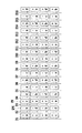
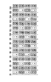
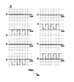
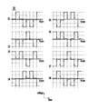
図3乃至図8は本発明の第1実施形態による液晶表示装置の極性配置及び反転駆動を示す図である。 3 to 8 are diagrams illustrating the polarity arrangement and inversion driving of the liquid crystal display device according to the first embodiment of the present invention.
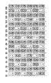
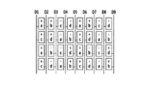
図面において長い縦線は実質的に互いに平行に配列されたデータラインを示し、四角形は副画素を示す。短い横線はデータラインと副画素の接続を示す。四角形内の正(+)または負(−)は特定時点で各副画素に印加されるデータ電圧の極性(以下、“副画素の極性”という)を示し、a、b、c及びdは各副画素が表現する色を示す。以下の図面でもこのような規則は同一に適用される。 In the drawing, long vertical lines indicate data lines arranged substantially parallel to each other, and squares indicate sub-pixels. A short horizontal line indicates a connection between the data line and the sub-pixel. The positive (+) or negative (−) in the square indicates the polarity of the data voltage applied to each subpixel at a specific time (hereinafter referred to as “subpixel polarity”), and a, b, c, and d are each Indicates the color expressed by the sub-pixel. Such rules apply equally to the following drawings.
まず、図3及び図4に示すように、図3は前記液晶表示装置のn番目フレームでの極性配置を示し、図4はn+1番目フレームでの極性配置を示す。各副画素が表現する色であるa、b、c及びdの色は全て異なってもよく、これらのうちの一対の色が同一であってもよく(例えば、aとcの色が同一)、二対の色が同一であってもよい(例えば、aとcの色が同一であり、bとdの色が同一)。一方、a、b、c及びdの色の4つの副画素が1つの画素をなしてもよく、a及びbの色の2つ副画素またはc及びdの色の2つの副画素が1つの画素をなしてもよい。以下、a、b、c及びdの色が全て異なり、4つの副画素が1つの画素をなす場合を例にして本発明の実施形態について詳細に説明する。 First, as shown in FIGS. 3 and 4, FIG. 3 shows the polarity arrangement in the nth frame of the liquid crystal display device, and FIG. 4 shows the polarity arrangement in the (n + 1) th frame. The colors a, b, c, and d that are colors represented by the sub-pixels may be all different, and a pair of colors may be the same (for example, the colors of a and c are the same). The two pairs of colors may be the same (for example, the colors a and c are the same, and the colors b and d are the same). On the other hand, four sub-pixels of a, b, c, and d colors may form one pixel, and two sub-pixels of a and b colors or two sub-pixels of c and d colors are one You may make a pixel. Hereinafter, an embodiment of the present invention will be described in detail by taking as an example a case in which all colors a, b, c, and d are different and four sub-pixels form one pixel.
それぞれのデータラインは全てその右側に位置する副画素に接続されている。実施形態によってはそれぞれのデータラインは全てその左側に位置する副画素に接続されてもよく、あるデータラインはその右側に位置する副画素に接続され、あるデータラインはその左側に位置する副画素に接続されてもよい。 Each data line is all connected to a subpixel located on the right side thereof. In some embodiments, each data line may be connected to a subpixel located on the left side of the data line, a data line may be connected to a subpixel located on the right side, and a data line may be connected to a subpixel located on the left side. May be connected.
データラインの観点で、n番目フレームで、第1、第3、第6及び第8データラインD1、D3、D6、D8には正(+)のデータ電圧が印加され、第2、第4、第5及び第7データラインD2、D4、D5、D7には負(−)のデータ電圧が印加される。反対に、n+1番目フレームでは第1、第3、第6及び第8データラインD1、D3、D6、D8には負(−)のデータ電圧が印加され、第2、第4、第5及び第7データラインD2、D4、D5、D7には正(+)のデータ電圧が印加される。 From the viewpoint of the data line, a positive (+) data voltage is applied to the first, third, sixth, and eighth data lines D1, D3, D6, and D8 in the nth frame, and the second, fourth, A negative (−) data voltage is applied to the fifth and seventh data lines D2, D4, D5, and D7. On the other hand, in the (n + 1) th frame, a negative (−) data voltage is applied to the first, third, sixth and eighth data lines D1, D3, D6 and D8, and the second, fourth, fifth and fifth data lines are applied. The positive (+) data voltage is applied to the seven data lines D2, D4, D5, and D7.
前記のようにデータラインによって極性を異にするデータ電圧の印加は8つのデータラインを基準に繰り返される。即ち、左側データラインからそれぞれのデータラインに正(+)、負(−)、正(+)、負(−)、負(−)、正(+)、負(−)及び正(+)のデータ電圧が印加されることが繰り返される。したがって、第1乃至第8データラインD1−D8に印加される前記データ電圧の極性は第9乃至第16データラインD9−D16にも同一に適用される。第1実施形態による反転駆動のためにデータ駆動部はフレームごとに極性が反転されるデータ電圧を前述の極性に合うようにそれぞれのデータラインに印加する。 As described above, the application of data voltages having different polarities depending on the data lines is repeated based on the eight data lines. That is, from the left data line to each data line, positive (+), negative (-), positive (+), negative (-), negative (-), positive (+), negative (-) and positive (+) The data voltage is applied repeatedly. Accordingly, the polarity of the data voltage applied to the first to eighth data lines D1-D8 is equally applied to the ninth to sixteenth data lines D9-D16. For the inversion driving according to the first embodiment, the data driving unit applies a data voltage whose polarity is inverted for each frame to each data line so as to match the aforementioned polarity.
副画素の観点で、第1乃至第4列にある副画素は隣接副画素間で極性が反転され、第5乃至第8列にある副画素も隣接副画素間で極性が反転されるが、第5乃至第8列にある副画素の極性は第1乃至第4列にある副画素と極性が反対である。第1乃至第8副画素列は極性が繰り返される基本単位を構成して行方向に繰り返される。即ち、第9乃至第16副画素列の極性は第1乃至第8副画素列の極性と順次に同一である。 In terms of subpixels, the subpixels in the first to fourth columns are inverted in polarity between adjacent subpixels, and the subpixels in the fifth to eighth columns are also inverted in polarity between adjacent subpixels. The polarities of the subpixels in the fifth to eighth columns are opposite to those of the subpixels in the first to fourth columns. The first to eighth subpixel columns form a basic unit in which the polarity is repeated and are repeated in the row direction. That is, the polarities of the ninth to sixteenth subpixel columns are sequentially the same as the polarities of the first to eighth subpixel columns.
全ての色の副画素に所定レベルのデータ電圧を印加する場合、n番目フレームで、色ごとに正(+)の副画素の個数と負(−)の副画素の個数が同一である。また、行方向に色ごとに正(+)の副画素と負(−)の副画素が互いに交互に配置されている。例えば、2つの基本単位でa色副画素は4つの副画素ごとに1つずつ位置し、その極性は左側から正(+)、負(−)、正(+)及び負(−)である。したがって正の極性、負の極性が均等に混ざっているので、極性間に存在可能な輝度差による表示品質の低下が発生しない。 When a predetermined level of data voltage is applied to all color sub-pixels, the number of positive (+) sub-pixels and the number of negative (-) sub-pixels are the same for each color in the nth frame. Further, positive (+) sub-pixels and negative (-) sub-pixels are alternately arranged for each color in the row direction. For example, in two basic units, one a-color subpixel is located for every four subpixels, and the polarity is positive (+), negative (-), positive (+), and negative (-) from the left side. . Therefore, since the positive polarity and the negative polarity are evenly mixed, the display quality is not deteriorated due to a luminance difference that can exist between the polarities.
n+1番目フレームでも、n番目フレームと同様に、色ごとに正(+)の副画素の個数と負(−)の副画素の個数が同一であり、行方向に色ごとに正(+)の副画素と負(−)の副画素が互いに交互に配置されている。したがって、極性不調和によるフレーム間の輝度差(例えば、同一レベルのデータ電圧が印加されても極性によって輝度が異なることがある)が存在しないので、フリッカー(flicker)が発生しない。 In the (n + 1) th frame, as in the nth frame, the number of positive (+) subpixels and the number of negative (−) subpixels are the same for each color, and positive (+) for each color in the row direction. Sub-pixels and negative (-) sub-pixels are alternately arranged. Accordingly, since there is no luminance difference between frames due to polarity inconsistency (for example, the luminance may vary depending on the polarity even when a data voltage of the same level is applied), flicker does not occur.
一方、それぞれの副画素列にある副画素は同一なデータラインに接続されている。その結果、一副画素列の副画素が互いに異なるデータラインに接続される場合、互いに異なるデータラインに接続される副画素間に発生可能な、薄膜トランジスタのゲートとソース間のキャパシタンス(Cgs)のような特性偏差による輝度差が発生しない。 On the other hand, the subpixels in each subpixel column are connected to the same data line. As a result, when sub-pixels of one sub-pixel column are connected to different data lines, the capacitance (Cgs) between the gate and the source of the thin film transistor that can be generated between the sub-pixels connected to different data lines. Difference in luminance due to characteristic deviation does not occur.
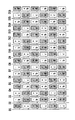
図5及び図6は1つの色のみを表示する場合のn番目フレームとn+1番目フレームの極性配置をそれぞれ示す。例えば、aが赤色である場合、赤色画面を表示する場合である。図面において斜線を施した副画素は該当副画素に最低階調のデータ電圧が印加される場合を示し、以下の図面でも同一に適用される。赤色aを表現する副画素の極性がn番目フレームとn+1番目フレームで反転されても、各フレームで正(+)の副画素と負(−)の副画素が交互に同一な個数で配置されている。したがって、単色を表示する場合にもフレーム間に輝度差が発生しない。 FIGS. 5 and 6 show the polarity arrangements of the nth frame and the (n + 1) th frame, respectively, when only one color is displayed. For example, when a is red, a red screen is displayed. The hatched subpixels in the drawings indicate a case where the data voltage of the lowest gradation is applied to the corresponding subpixels, and the same applies in the following drawings. Even if the polarities of the subpixels expressing red a are inverted in the nth frame and the n + 1th frame, the same number of positive (+) subpixels and negative (−) subpixels are alternately arranged in each frame. ing. Therefore, even when displaying a single color, no luminance difference occurs between frames.
図7及び図8は混色を表示する場合のn番目フレームとn+1番目フレームの極性配置をそれぞれ示す。例えば、a、b、c及びdがそれぞれ赤色、緑色、青色及び白色であり、青緑色(cyan)を表示する場合である。緑色b及び青色cをそれぞれ表現する副画素の極性がn番目フレームとn+1番目フレームで反転されても、各フレームで正(+)の副画素と負(−)の副画素が交互に同一な個数で配置されている。したがって、混色を表示する場合にもフレーム間に輝度差が発生しない。 FIG. 7 and FIG. 8 respectively show the polarity arrangements of the nth frame and the (n + 1) th frame when displaying mixed colors. For example, a, b, c, and d are red, green, blue, and white, respectively, and blue-green (cyan) is displayed. Even if the polarities of the subpixels representing green b and blue c are inverted in the nth frame and the n + 1th frame, the positive (+) subpixel and the negative (−) subpixel are alternately the same in each frame. Arranged by number. Therefore, no luminance difference occurs between frames even when displaying mixed colors.
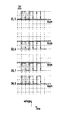
図9乃至図11は本発明の第1実施形態による液晶表示装置でデータラインに印加されるデータ電圧の例を示す図である。 9 to 11 are diagrams illustrating examples of data voltages applied to the data lines in the liquid crystal display device according to the first embodiment of the present invention.
図9は全ての副画素に同一なデータ電圧、例えば、最大階調電圧を印加する場合のデータラインに印加されるデータ電圧を示す。図面において横方向への1つの目盛りは1水平期間1Hを示す。第1データラインD1に印加される電圧と第2データラインD2に印加される電圧は大きさが同一であり、極性は反対である。第3及び第4データラインD3、D4の対、第5及び第6データラインD5、D6の対、そして第7及び第8データラインD7、D8の対にもこのような関係は同一である。したがって、データラインにデータ電圧が相補的(即ち、大きさが同一であり、極性が反対である)に印加されるので、データ電圧の極性が均衡をなす。その結果、データ電圧の極性がいずれか一方に偏らないので、共通電圧Vcomに影響を与えない。
FIG. 9 shows the data voltage applied to the data line when the same data voltage, for example, the maximum gradation voltage is applied to all the sub-pixels. In the drawing, one scale in the horizontal direction indicates one
図10はb色(例えば、緑色)の副画素にのみ最大階調電圧を印加し、残り色の副画素には最低階調電圧を印加して単色を表示する場合のデータラインに印加されるデータ電圧を示す。図10に示されているように、第1及び第3データラインD1、D3に印加される電圧と第5及び第7データラインD5、D7に印加されるデータ電圧は大きさが同一であり、極性が反対である。第2データラインD2に印加される電圧は第6データラインD6に印加される電圧と大きさが同一であり、極性が反対であるだけでなく、いずれか一方の電圧上昇(rising)時、他の一方の電圧は下降(falling)する。同様に、第4データラインD4に印加される電圧は第8データラインD8に印加される電圧と大きさが同一であり、極性が反対であり、いずれか一方の電圧上昇時、他の一方の電圧が下降する。したがって、データラインに電圧が相補的に印加され、また、電圧の上昇及び下降を相殺するように印加されるので、単色表示時にデータ電圧の極性がいずれか一方に偏らないので、共通電圧Vcomに影響を与えない。 In FIG. 10, the maximum gradation voltage is applied only to the sub-pixel of b color (for example, green), and the minimum gradation voltage is applied to the sub-pixels of the remaining color to be applied to the data line when displaying a single color. Indicates the data voltage. As shown in FIG. 10, the voltages applied to the first and third data lines D1 and D3 and the data voltages applied to the fifth and seventh data lines D5 and D7 have the same magnitude. The polarity is opposite. The voltage applied to the second data line D2 has the same magnitude as the voltage applied to the sixth data line D6, and not only has the opposite polarity, but also when one of the voltages rises, One of the voltages falls. Similarly, the voltage applied to the fourth data line D4 is the same in magnitude as the voltage applied to the eighth data line D8 and has the opposite polarity, and when one of the voltages rises, the other one The voltage drops. Therefore, since the voltage is applied to the data line in a complementary manner and is applied so as to cancel the rise and fall of the voltage, the polarity of the data voltage is not biased to either one at the time of monochromatic display. Does not affect.
図11はb色(例えば、緑色)及びc色(例えば、青色)の副画素に最大階調電圧を印加し、残り色の副画素には最低階調電圧を印加して混色(例えば、青緑色)を表示する場合のデータラインに印加されるデータ電圧を示す。第1データラインD1と第5データラインD5には互いに相補的に、そして相殺的(即ち、いずれか一方の電圧上昇時、他の一方の電圧下降)に電圧が印加される。このような関係は第2及び第6データラインD2、D6間に、第3及び第7データラインD3、D7間に、そして第4及び第8データラインD4、D8間にも同一に示されることが分かる。したがって、データラインに電圧が相補的に印加され、また、電圧の上昇及び下降を相殺するように印加されるので、データ電圧がいずれか一方に偏らないので、混色表示時にも共通電圧Vcomに影響を与えない。 In FIG. 11, the maximum gradation voltage is applied to the sub-pixels of b color (for example, green) and c color (for example, blue), and the minimum gradation voltage is applied to the sub-pixels of the remaining colors to mix colors (for example, blue The data voltage applied to the data line when displaying (green) is shown. A voltage is applied to the first data line D1 and the fifth data line D5 in a complementary manner and in a destructive manner (that is, when one of the voltages increases, the other decreases). Such a relationship is the same between the second and sixth data lines D2 and D6, between the third and seventh data lines D3 and D7, and between the fourth and eighth data lines D4 and D8. I understand. Therefore, the voltage is applied to the data lines in a complementary manner, and is applied so as to cancel the rise and fall of the voltage, so the data voltage is not biased to either one, so that the common voltage Vcom is also affected during mixed color display. Not give.
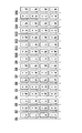
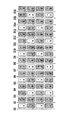
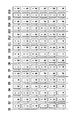
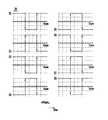
図12乃至図17は本発明の第2実施形態による液晶表示装置の極性配置及び反転駆動を示す図である。 12 to 17 are diagrams illustrating polarity arrangement and inversion driving of the liquid crystal display device according to the second embodiment of the present invention.
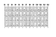
図12及び図13はそれぞれ前記液晶表示装置でn番目フレーム及びn+1番目フレームの極性配置を示す。 12 and 13 show the polarity arrangement of the nth frame and the (n + 1) th frame in the liquid crystal display device, respectively.
第2実施形態を説明することにおいて、第1実施形態と同一な技術的特徴については説明を簡略化又は省略する。前述の第1実施形態と同様に、それぞれのデータラインは全てその右側に位置する副画素に接続されている。したがって副画素間に薄膜トランジスタのCgsのような特性偏差による輝度差が発生しない。実施形態によってはそれぞれのデータラインは全てその左側に位置する副画素に接続されているか、あるデータラインはその右側にのみ位置する副画素に接続されており、あるデータラインはその左側にのみ位置する副画素に接続されていてもよい。 In describing the second embodiment, the description of the technical features that are the same as those of the first embodiment will be simplified or omitted. Similar to the first embodiment described above, each data line is all connected to a sub-pixel located on the right side thereof. Therefore, a luminance difference due to a characteristic deviation such as Cgs of a thin film transistor does not occur between subpixels. In some embodiments, each data line is connected to a subpixel located on the left side of the data line, or a data line is connected to a subpixel located only on the right side of the data line, and a data line is located only on the left side of the data line. May be connected to the subpixel.
データラインの観点で、n番目フレームで、第1、第3、第6及び第8データラインD1、D3、D6、D8には3つの副画素ごとに正(+)のデータ電圧と負(−)のデータ電圧が印加されることを繰り返し、第2、第4、第5及び第7データラインD2、D4、D5、D7には3つの副画素ごとに負(−)のデータ電圧と正(+)のデータ電圧が印加されることを繰り返す。即ち、第1実施形態とは異なり、第2実施形態では1フレーム全体に亘って該当データラインに同一な極性のデータ電圧が印加されるのではなく、3つの副画素ごとに極性が反転されるように印加される。例えば、該当データラインの第1乃至第3ゲートラインに接続された副画素には正(+)のデータ電圧が印加され、第4乃至第6ゲートラインに接続された副画素には負(−)のデータ電圧が印加され、このような反転駆動(いわゆる3ライン反転駆動)は該当データラインに対して繰り返される。 From the viewpoint of the data line, in the nth frame, the first, third, sixth and eighth data lines D1, D3, D6 and D8 have a positive (+) data voltage and a negative (− ) Is repeatedly applied, and the second, fourth, fifth, and seventh data lines D2, D4, D5, and D7 have a negative (−) data voltage and a positive (−) for every three subpixels. (+) The data voltage is repeatedly applied. That is, unlike the first embodiment, in the second embodiment, the data voltage having the same polarity is not applied to the corresponding data line over the entire frame, but the polarity is inverted every three sub-pixels. Is applied as follows. For example, a positive (+) data voltage is applied to the subpixels connected to the first to third gate lines of the corresponding data line, and a negative (−) is applied to the subpixels connected to the fourth to sixth gate lines. ) Is applied, and such inversion driving (so-called three-line inversion driving) is repeated for the corresponding data line.
n+1番目フレームではn番目フレームと反対にデータ電圧が印加される。即ち、第1、第3、第6及び第8データラインD1、D3、D6、D8には3つの副画素ごとに負(−)のデータ電圧と正(+)のデータ電圧が印加されることを繰り返し、第2、第4、第5及び第7データラインD2、D4、D5、D7には同様に3つの副画素ごとに正(+)のデータ電圧と負(−)のデータ電圧が印加されることを繰り返す。 In the (n + 1) th frame, the data voltage is applied opposite to the nth frame. That is, a negative (−) data voltage and a positive (+) data voltage are applied to the first, third, sixth, and eighth data lines D1, D3, D6, and D8 for every three subpixels. The positive (+) data voltage and the negative (−) data voltage are applied to the second, fourth, fifth, and seventh data lines D2, D4, D5, and D7 in the same manner for each of the three subpixels. To be repeated.
前述のようにデータラインによって、そして3つのゲートラインごとに極性を異にするデータ電圧の印加は8つのデータラインを基準に繰り返される。したがって、第1乃至第8データラインD1−D8に印加される前記データ電圧の極性は第9乃至第16データラインD9−D16にも同一に適用される。第2実施形態による反転駆動のために、データ駆動部はそれぞれのデータラインにフレームごとに極性が反転され、また、1フレームで3つのゲートラインごとに極性が反転されるデータ電圧を前述の極性に合うように印加してもよい。 As described above, the application of data voltages having different polarities by the data lines and every three gate lines is repeated with reference to the eight data lines. Accordingly, the polarity of the data voltage applied to the first to eighth data lines D1-D8 is equally applied to the ninth to sixteenth data lines D9-D16. For the inversion driving according to the second embodiment, the data driving unit applies a data voltage whose polarity is inverted every frame to each data line and whose polarity is inverted every three gate lines in one frame. You may apply so that it may be suitable.
副画素の観点で、第1乃至第4列にある副画素は隣接副画素間で極性が反転され、第5乃至第8列にある副画素も隣接副画素間で極性が反転されるが、第5乃至第8列にある副画素の極性は第1乃至第4列にある副画素と極性が反対である。また、第1乃至第8列にある副画素はそれぞれの列で3つの副画素ごとに極性が反転される。第1乃至第8副画素列は基本単位を構成して行方向に繰り返される。即ち、第9乃至第16副画素列の極性は第1乃至第8副画素列の極性と順次に同一である。 In terms of subpixels, the subpixels in the first to fourth columns are inverted in polarity between adjacent subpixels, and the subpixels in the fifth to eighth columns are also inverted in polarity between adjacent subpixels. The polarities of the subpixels in the fifth to eighth columns are opposite to those of the subpixels in the first to fourth columns. The subpixels in the first to eighth columns are inverted in polarity every three subpixels in each column. The first to eighth subpixel columns constitute a basic unit and are repeated in the row direction. That is, the polarities of the ninth to sixteenth subpixel columns are sequentially the same as the polarities of the first to eighth subpixel columns.
第1実施形態と同様に、全ての色の副画素に所定レベルのデータ電圧を印加する場合、n番目はもちろんn+1番目フレーム(したがって、全てのフレーム)で、色ごとに正(+)の副画素の個数と負(−)の副画素の個数が同一であり、行方向に色ごとに正(+)の副画素と負(−)の副画素が交互に配置されている。したがって正の極性、負の極性が均等に混ざっているので、極性間に存在可能な輝度差による表示品質低下が発生せず、極性不調和によるフレーム間の輝度差も発生しない。 As in the first embodiment, when a predetermined level of data voltage is applied to all color sub-pixels, the n + th (and therefore all) frames of the nth as well as the positive (+) sub-color for each color. The number of pixels is the same as the number of negative (−) subpixels, and positive (+) subpixels and negative (−) subpixels are alternately arranged for each color in the row direction. Accordingly, since the positive polarity and the negative polarity are evenly mixed, the display quality is not deteriorated due to the luminance difference that can exist between the polarities, and the luminance difference between frames due to the polarity inconsistency does not occur.
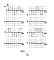
図14及び図15は1つの色のみを表示する場合のn番目フレームとn+1番目フレームの極性配置をそれぞれ示す。例えば、aが赤色である場合、赤色aを表現する副画素の極性がn番目フレームとn+1番目フレームで反転されても、各フレームで正(+)の副画素と負(−)の副画素が交互に同一な個数で配置されている。したがって単色を表示する場合にもフレーム間に輝度差が発生しない。 FIG. 14 and FIG. 15 show the polar arrangement of the nth frame and the (n + 1) th frame when only one color is displayed. For example, when a is red, even if the polarity of the subpixel representing red a is inverted between the nth frame and the n + 1th frame, the positive (+) subpixel and the negative (−) subpixel in each frame. Are alternately arranged in the same number. Therefore, no luminance difference occurs between frames even when displaying a single color.
図16及び図17は混色を表示する場合のn番目フレームとn+1番目フレームの極性配置をそれぞれ示す。例えば、a、b、c及びdがそれぞれ赤色、緑色、青色及び白色である場合、緑色(b)及び青色(c)をそれぞれ表現する副画素の極性がn番目フレームとn+1番目フレームで反転されても、各フレームで正(+)の副画素と負(−)の副画素が交互に同一な個数で配置されている。したがって混色を表示する場合にもフレーム間に輝度差が発生しない。 FIGS. 16 and 17 show the polar arrangements of the nth frame and the (n + 1) th frame, respectively, when displaying a mixed color. For example, if a, b, c, and d are red, green, blue, and white, respectively, the polarities of the sub-pixels that represent green (b) and blue (c) are inverted in the nth frame and the n + 1th frame, respectively. Even in each frame, positive (+) sub-pixels and negative (-) sub-pixels are alternately arranged in the same number. Therefore, no luminance difference occurs between frames when displaying mixed colors.
図18乃至図20は本発明の第2実施形態による液晶表示装置でデータラインに印加されるデータ電圧の例を示す図である。 18 to 20 are diagrams showing examples of data voltages applied to the data lines in the liquid crystal display device according to the second embodiment of the present invention.
図18は全ての副画素に同一なデータ電圧、例えば、最大階調電圧を印加する場合のデータラインに印加されるデータ電圧を示す。第1データラインD1に印加される電圧と第2データラインD2に印加される電圧は大きさが同一であり、極性は反対であり、ある一電圧の上昇時、他の一電圧は下降する。したがって第1及び第2データラインD1、D2に印加される電圧は相補的であり相殺的である。同様に、第3及び第4データラインD3、D4、第5及び第6データラインD5、D6、そして第7及び第8データラインD7、D8にそれぞれ印加されるデータ電圧も相補的であり相殺的である。したがってデータ電圧がいずれか一方に偏らないので、共通電圧Vcomに影響を与えない。 FIG. 18 shows the data voltage applied to the data line when the same data voltage, for example, the maximum gradation voltage is applied to all the sub-pixels. The voltage applied to the first data line D1 and the voltage applied to the second data line D2 are the same in magnitude and opposite in polarity. When one voltage increases, the other voltage decreases. Therefore, the voltages applied to the first and second data lines D1 and D2 are complementary and offset. Similarly, the data voltages applied to the third and fourth data lines D3 and D4, the fifth and sixth data lines D5 and D6, and the seventh and eighth data lines D7 and D8, respectively, are complementary and offset. It is. Therefore, since the data voltage is not biased to either one, the common voltage Vcom is not affected.
図19はa色(例えば、赤色)の副画素にのみ最大階調電圧を印加し、残り色の副画素には最低階調電圧を印加して単色を表示する場合のデータラインに印加されるデータ電圧を示す。図19に示されているように、第1及び第5データラインD1、D5、第2及び第6データラインD2、D6、第3及び第7データラインD3、D7、そして第4及び第8データラインD4、D8のそれぞれの対にデータ電圧が相補的で相殺的に印加される。したがって単色表示時にデータ電圧がいずれか一方に偏らず均衡をなす。 In FIG. 19, the maximum gradation voltage is applied only to the a-color (for example, red) subpixel, and the minimum gradation voltage is applied to the remaining color subpixels to be applied to the data line when displaying a single color. Indicates the data voltage. As shown in FIG. 19, the first and fifth data lines D1, D5, the second and sixth data lines D2, D6, the third and seventh data lines D3, D7, and the fourth and eighth data. A data voltage is applied to each pair of lines D4 and D8 in a complementary and destructive manner. Therefore, the data voltage is balanced to either one at the time of monochromatic display.
図20はb色(例えば、緑色)及びc色(例えば、青色)の副画素に最大階調電圧を印加し、残り色の副画素には最低階調電圧を印加して混色(例えば、青緑色)を表示する場合のデータラインに印加されるデータ電圧を示す。第1及び第8データラインD1、D8と第4及び第5データラインD4、D5にはデータ電圧が相補的で相殺的に印加される。また、第2及び第7データラインD2、D7と第3及び第6データラインD3、D6にはデータ電圧が相補的で相殺的に印加される。したがって、データ電圧がいずれか一方に偏らないので、混色表示時にも共通電圧Vcomに影響を与えない。 In FIG. 20, the maximum gradation voltage is applied to the sub-pixels of b color (for example, green) and c color (for example, blue), and the minimum gradation voltage is applied to the sub-pixels of the remaining colors to mix colors (for example, blue The data voltage applied to the data line when displaying (green) is shown. Data voltages are applied to the first and eighth data lines D1 and D8 and the fourth and fifth data lines D4 and D5 in a complementary and destructive manner. In addition, data voltages are applied to the second and seventh data lines D2 and D7 and the third and sixth data lines D3 and D6 in a complementary and destructive manner. Therefore, since the data voltage is not biased to either one, the common voltage Vcom is not affected even when displaying mixed colors.
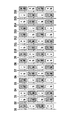
図21乃至図26は本発明の他の実施形態による液晶表示装置の極性配置を示す図である。 FIG. 21 to FIG. 26 are diagrams illustrating the polarity arrangement of a liquid crystal display device according to another embodiment of the present invention.
図21には本発明の第3実施形態による極性配置が示される。それぞれのデータラインはその右側と左側に位置する副画素に1つずつ交互に接続されている。あるフレーム(例えば、n番目フレーム)で、第1及び第2データラインD1、D2には正(+)のデータ電圧が印加され、第3及び第4データラインD3、D4には負(−)のデータ電圧が印加される。このようなデータ電圧の印加は4つのデータラインを基本単位にして行方向に繰り返される。したがって第5乃至第8データラインD5−D8には第1乃至第4データラインD1−D4に印加される極性のデータ電圧が印加される。 FIG. 21 shows a polarity arrangement according to the third embodiment of the present invention. Each data line is alternately connected one by one to the subpixels located on the right and left sides. In a certain frame (for example, the nth frame), a positive (+) data voltage is applied to the first and second data lines D1 and D2, and a negative (-) is applied to the third and fourth data lines D3 and D4. The data voltage is applied. Such application of the data voltage is repeated in the row direction with four data lines as a basic unit. Therefore, the data voltage having the polarity applied to the first to fourth data lines D1-D4 is applied to the fifth to eighth data lines D5-D8.
データラインがその右側及び左側に位置する副画素に交互に接続されているので、第1列の副画素には全て正(+)の電圧が印加され、第3列の副画素には全て負(−)の電圧が印加されるが、第2列の副画素には正(+)と負(−)の電圧が交互に印加され、第4列の副画素には負(−)と正(+)の電圧が交互に印加される。その次のフレームではそれぞれのデータラインに現在のフレームに印加される電圧と異なる極性の電圧が印加され、それぞれの副画素も極性が反転される。 Since the data lines are alternately connected to the subpixels located on the right and left sides thereof, a positive (+) voltage is applied to all the subpixels in the first column and all the subpixels in the third column are negative. (−) Voltage is applied, but positive (+) and negative (−) voltages are alternately applied to the second column of subpixels, and negative (−) and positive are applied to the fourth column of subpixels. A voltage of (+) is applied alternately. In the next frame, a voltage having a polarity different from that applied to the current frame is applied to each data line, and the polarity of each subpixel is also inverted.
図22には本発明の第4実施形態による極性配置が示される。それぞれのデータラインはその右側と左側に位置する副画素に1つずつ交互に接続されている。あるフレームで、第1、第3、第6及び第8データラインD1、D3、D6、D8には正(+)のデータ電圧と負(−)のデータ電圧が3つの副画素ごとに交互に印加され、第2、第4、第5及び第7データラインD2、D4、D5、D7には負(−)のデータ電圧と正(+)のデータ電圧が3つの副画素ごとに交互に印加される。このようなデータ電圧の印加は8つのデータラインを基本単位にして行方向に繰り返され、フレームごとに各データラインに印加されるデータ電圧の極性が反転される。 FIG. 22 shows a polarity arrangement according to the fourth embodiment of the present invention. Each data line is alternately connected one by one to the subpixels located on the right and left sides. In one frame, the first, third, sixth, and eighth data lines D1, D3, D6, and D8 have a positive (+) data voltage and a negative (−) data voltage alternately every three sub-pixels. Applied to the second, fourth, fifth, and seventh data lines D2, D4, D5, and D7, a negative (−) data voltage and a positive (+) data voltage are alternately applied to every three sub-pixels. Is done. Such application of the data voltage is repeated in the row direction with 8 data lines as a basic unit, and the polarity of the data voltage applied to each data line is inverted every frame.
データラインがその右側及び左側に位置する副画素に交互に接続されているため、第1乃至第3列及び第5乃至第7列の副画素は3つの副画素を繰り返し単位にし、各繰り返し単位で隣接副画素間で極性が反転されるが、第4及び第8列の副画素は3つの副画素ごとに極性が反転される。 Since the data lines are alternately connected to the subpixels located on the right and left sides thereof, the subpixels in the first to third columns and the fifth to seventh columns have three subpixels as repeating units, and each repeating unit The polarity is inverted between adjacent subpixels, but the polarity of the subpixels in the fourth and eighth columns is inverted every three subpixels.
図23には本発明の第5実施形態による極性配置が示される。それぞれのデータラインはその右側と左側に位置する副画素に1つずつ交互に接続されている。あるフレームで、第1乃至第4データラインD1−D4には正(+)のデータ電圧と負(−)のデータ電圧が3つの副画素ごとに交互に印加され、第5乃至第8データラインD5−D8には負(−)のデータ電圧と正(+)のデータ電圧が3つの副画素ごとに交互に印加される。このようなデータ電圧の印加は8つのデータラインを基本単位にして行方向に繰り返され、フレームごとに反転される。 FIG. 23 shows a polarity arrangement according to the fifth embodiment of the present invention. Each data line is alternately connected one by one to the subpixels located on the right and left sides. In one frame, positive (+) data voltage and negative (−) data voltage are alternately applied to the first to fourth data lines D1 to D4 for every three sub-pixels, and the fifth to eighth data lines. A negative (−) data voltage and a positive (+) data voltage are alternately applied to D5-D8 every three subpixels. Such application of the data voltage is repeated in the row direction with eight data lines as a basic unit, and is inverted every frame.
データラインがその右側及び左側に位置する副画素に交互に接続されているため、第1乃至第3列及び第5乃至第7列の副画素は3つの副画素ごとに極性が反転されるが、第4列及び第8列の副画素は3つの副画素を繰り返し単位にして各繰り返し単位で隣接副画素間で極性が反転される。 Since the data lines are alternately connected to the subpixels located on the right and left sides, the subpixels in the first to third columns and the fifth to seventh columns are inverted in polarity every three subpixels. The subpixels in the fourth column and the eighth column have three subpixels as a repeating unit, and the polarity is inverted between adjacent subpixels in each repeating unit.
第3乃至第5実施形態による極性配置で、色ごとに正(+)の副画素の個数と負(−)の副画素の個数が同一であり、行方向に色ごとに正(+)の副画素と負(−)の副画素が互いに交互に配置されている。また、白色、単色、または混色を表示する場合、データラインに電圧が相補的で相殺的に印加される。したがって極性不調和による輝度差や極性偏りによる共通電圧のリップルが発生しない。 In the polarity arrangement according to the third to fifth embodiments, the number of positive (+) subpixels and the number of negative (−) subpixels are the same for each color, and positive (+) for each color in the row direction. Sub-pixels and negative (-) sub-pixels are alternately arranged. In addition, when displaying white, single color, or mixed color, voltages are applied to the data lines in a complementary and destructive manner. Therefore, there is no common voltage ripple due to luminance difference or polarity bias due to polarity mismatch.
図24には本発明の第6実施形態による極性配置が示される。それぞれのデータラインはその右側と左側に位置する副画素に2つずつ交互に接続されている。あるフレームで、第1及び第2データラインD1、D2には正(+)のデータ電圧が印加され、第3及び第4データラインD3、D4には負(−)のデータラインが印加される。このようなデータ電圧の印加は4つのデータラインを基本単位にして行方向に繰り返される。 FIG. 24 shows a polarity arrangement according to the sixth embodiment of the present invention. Each data line is alternately connected to the subpixels located on the right side and the left side of the data line. In a certain frame, a positive (+) data voltage is applied to the first and second data lines D1 and D2, and a negative (−) data line is applied to the third and fourth data lines D3 and D4. . Such application of the data voltage is repeated in the row direction with four data lines as a basic unit.
前記のような反転駆動においてデータラインがその右側及び左側に位置する副画素に2つずつ交互に接続されているので、第1列の副画素には全て正(+)の電圧が印加され、第3列の副画素には全て負(−)の電圧が印加されるが、第2列の副画素には2つの副画素ごとに正(+)と負(−)の電圧が交互に印加され、第4列の副画素には2つの副画素ごとに負(−)と正(+)の電圧が交互に印加される。その次のフレームではそれぞれのデータラインに現在のフレームに印加される電圧と異なる極性の電圧が印加され、それぞれの副画素も極性が反転される。 In the inversion driving as described above, since the data lines are alternately connected to the subpixels located on the right side and the left side thereof, a positive (+) voltage is applied to all the subpixels in the first column, A negative (-) voltage is applied to all the subpixels in the third column, but a positive (+) and a negative (-) voltage are alternately applied to the subpixels in the second column every two subpixels. Then, negative (−) and positive (+) voltages are alternately applied to the subpixels in the fourth column every two subpixels. In the next frame, a voltage having a polarity different from that applied to the current frame is applied to each data line, and the polarity of each subpixel is also inverted.
図25には本発明の第7実施形態による極性配置が示される。それぞれのデータラインはその右側と左側に位置する副画素に2つずつ交互に接続されている。あるフレームで、第1乃至第3データラインD1−D3には正(+)のデータ電圧と負(−)のデータ電圧が4つの副画素ごとに交互に印加され、第4乃至第6データラインD4−D6には負(−)のデータ電圧と正(+)のデータ電圧が4つの副画素ごとに交互に印加される。このようなデータ電圧の印加は6つのデータラインを基本単位にして行方向に繰り返され、フレームごとに反転される。各列の副画素は4つの副画素ごとに極性が反転されるが、第3列及び第6列の副画素は他の列の副画素と異なる周期で反転される。 FIG. 25 shows a polarity arrangement according to the seventh embodiment of the present invention. Each data line is alternately connected to the subpixels located on the right side and the left side of the data line. In one frame, a positive (+) data voltage and a negative (−) data voltage are alternately applied to the first to third data lines D1 to D3 every four sub-pixels, and the fourth to sixth data lines. A negative (−) data voltage and a positive (+) data voltage are alternately applied to D4-D6 every four subpixels. Such application of the data voltage is repeated in the row direction using six data lines as a basic unit, and is inverted every frame. The polarity of the subpixels in each column is inverted every four subpixels, but the subpixels in the third column and the sixth column are inverted at a different period from the subpixels in the other columns.
図26には本発明の第8実施形態による極性配置が示される。それぞれのデータラインはその右側と左側に位置する副画素に2つずつ交互に接続されている。あるフレームで、第1乃至第3データラインD1−D3には正(+)のデータ電圧が印加され、第4乃至第6データラインD4−D6には負(−)のデータ電圧が印加される。このようなデータ電圧の印加は6つのデータラインを基本単位にして行方向に繰り返される。その結果、第1及び第2列の副画素には正(+)のデータ電圧が印加され、第4及び第5列の副画素には負(−)のデータ電圧が印加され、第3列の副画素には2つの副画素ごとに正(+)のデータ電圧と負(−)のデータ電圧が交互に印加され、そして第6列の副画素には2つの副画素ごとに負(−)のデータ電圧と正(+)のデータ電圧が交互に印加される。その次のフレームではそれぞれの副画素に異なる極性のデータ電圧が印加される。 FIG. 26 shows a polarity arrangement according to the eighth embodiment of the present invention. Each data line is alternately connected to the subpixels located on the right side and the left side of the data line. In a certain frame, a positive (+) data voltage is applied to the first to third data lines D1-D3, and a negative (-) data voltage is applied to the fourth to sixth data lines D4-D6. . Such application of the data voltage is repeated in the row direction using six data lines as a basic unit. As a result, a positive (+) data voltage is applied to the first and second column sub-pixels, a negative (−) data voltage is applied to the fourth and fifth column sub-pixels, and the third column. A positive (+) data voltage and a negative (−) data voltage are alternately applied to every two sub-pixels, and negative (−) every two sub-pixels. ) Data voltage and positive (+) data voltage are alternately applied. In the next frame, data voltages having different polarities are applied to the respective sub-pixels.
第6乃至第8実施形態による極性配置で、同一な色を示す正(+)の副画素と負(−)の副画素が互いに交互に配置されない行もあるが、色ごとに正(+)の副画素の個数と負(−)の副画素の個数が同一で全体的に均衡をなす。また、白色、単色、または混色を表示する場合、データラインに電圧が相補的で相殺的に印加される。したがって、極性不調和による輝度差が実質的に発生せず、極性偏りによる共通電圧のリップルが発生しない。 In the polarity arrangement according to the sixth to eighth embodiments, there are rows in which positive (+) subpixels and negative (−) subpixels showing the same color are not alternately arranged, but positive (+) for each color. The number of sub-pixels and the number of negative (−) sub-pixels are the same and balance is achieved overall. In addition, when displaying white, single color, or mixed color, voltages are applied to the data lines in a complementary and destructive manner. Therefore, a luminance difference due to polarity inconsistency does not substantially occur, and a common voltage ripple due to polarity bias does not occur.
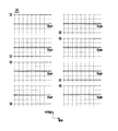
図27及び図28はデータ電圧の極性偏りが起こる液晶表示装置の極性配置及びデータラインに印加されるデータ電圧の例を示す図である。 27 and 28 are diagrams showing examples of the polarity arrangement of the liquid crystal display device in which the polarity deviation of the data voltage occurs and the data voltage applied to the data line.
図27に示すように、それぞれのデータラインはその右側に位置する副画素にのみ接続されている。あるフレームで、第1及び第4データラインには正(+)のデータ電圧が印加され、第2及び第3データラインには負(−)のデータ電圧が印加される。このようなデータ電圧の印加は6つのデータラインを基本単位にして行方向に繰り返され、フレームごとに反転される。 As shown in FIG. 27, each data line is connected only to the sub-pixel located on the right side thereof. In a certain frame, a positive (+) data voltage is applied to the first and fourth data lines, and a negative (−) data voltage is applied to the second and third data lines. Such application of the data voltage is repeated in the row direction using six data lines as a basic unit, and is inverted every frame.
このような極性配置においては極性偏りによって共通電圧でリップルが発生することがある。例えば図28には図27の副画素配置構造で混色を表示するためにa及びd色の副画素には最低階調電圧を印加し、b及びc色には最大階調電圧を印加することを例示する。図28に示されているように、あるデータラインに印加される電圧も相補的でないだけでなく、ある1つのデータラインの電圧が上昇する時に残りデータラインの電圧も上昇し、ある1つのデータラインの電圧が下降する時に残りデータラインの電圧も下降する。これによってデータ電圧の極性偏りが起こり、その結果、共通電圧が極性偏りに引かれて揺れるリップル現象が起こることがある。これは画質不良を誘発することがある。本発明の実施形態による極性配置による場合、このような極性偏りによる共通電圧のリップル現象や画質不良が発生しない。 In such a polarity arrangement, a ripple may occur at the common voltage due to the polarity deviation. For example, in FIG. 28, in order to display mixed colors in the subpixel arrangement structure of FIG. 27, the minimum gradation voltage is applied to the a and d color subpixels, and the maximum gradation voltage is applied to the b and c colors. Is illustrated. As shown in FIG. 28, not only the voltage applied to a certain data line is not complementary, but also when the voltage of one data line rises, the voltage of the remaining data line also rises. When the line voltage decreases, the remaining data line voltage also decreases. As a result, a polarity deviation of the data voltage occurs, and as a result, a ripple phenomenon in which the common voltage is swayed by the polarity deviation may occur. This can induce poor image quality. In the case of the polarity arrangement according to the embodiment of the present invention, the common voltage ripple phenomenon and the image quality defect due to the polarity deviation do not occur.
以上で本発明の好ましい実施形態について詳細に説明したが、本発明の権利範囲はこれに限定されるものではなく、次の請求範囲で定義している本発明の基本概念を用いた通常の技術者の様々な変形及び改良形態も本発明の権利範囲に属すると理解されなければならない。 The preferred embodiment of the present invention has been described in detail above, but the scope of the present invention is not limited to this, and a normal technique using the basic concept of the present invention defined in the following claims. It should be understood that various modifications and improvements of those skilled in the art also belong to the scope of the present invention.
1:液晶表示装置
3:液晶層
100:下部パネル
200:上部パネル
300:液晶表示パネル
400:ゲート駆動部
500:データ駆動部
600:信号制御部
D1−Dm:データライン
G1−Gn:ゲートライン
1: liquid crystal display device 3: liquid crystal layer 100: lower panel 200: upper panel 300: liquid crystal display panel 400: gate driver 500: data driver 600: signal controller D1-Dm: data line G1-Gn: gate line
Claims (10)
列方向に配列された複数のデータラインと、
前記ゲートライン及び前記データラインにそれぞれ接続され、行に沿って連続して配列されている8つの副画素を含む基本単位が行列方向に配列されている複数の副画素とを含み、
前記基本単位で、行に沿って一番目の副画素から四番目の副画素までは隣接副画素に印加される電圧の極性が反対であり、五番目の副画素から八番目の副画素までも隣接副画素に印加される電圧の極性が反対であるが、前記四番目の副画素と前記五番目の副画素に印加される電圧の極性は同一であることを特徴とする液晶表示装置。 A plurality of gate lines arranged in a row direction;
Multiple data lines arranged in columns,
A plurality of subpixels, each of which is connected to the gate line and the data line and includes eight subpixels arranged continuously along a row and arranged in a matrix direction;
In the basic unit, the polarity of the voltage applied to the adjacent subpixel is opposite from the first subpixel to the fourth subpixel along the row, and the fifth subpixel to the eighth subpixel are also opposite. A liquid crystal display device, wherein the polarities of voltages applied to adjacent subpixels are opposite, but the polarities of voltages applied to the fourth subpixel and the fifth subpixel are the same.
Applications Claiming Priority (2)
| Application Number | Priority Date | Filing Date | Title |
|---|---|---|---|
| KR1020130155780A KR102143926B1 (en) | 2013-12-13 | 2013-12-13 | Liquid crystal display and method for driving the same |
| KR10-2013-0155780 | 2013-12-13 |
Publications (2)
| Publication Number | Publication Date |
|---|---|
| JP2015114663A true JP2015114663A (en) | 2015-06-22 |
| JP6552181B2 JP6552181B2 (en) | 2019-07-31 |
Family
ID=53369209
Family Applications (1)
| Application Number | Title | Priority Date | Filing Date |
|---|---|---|---|
| JP2014226372A Active JP6552181B2 (en) | 2013-12-13 | 2014-11-06 | Liquid crystal display device and driving method thereof |
Country Status (5)
| Country | Link |
|---|---|
| US (1) | US9934736B2 (en) |
| JP (1) | JP6552181B2 (en) |
| KR (1) | KR102143926B1 (en) |
| CN (1) | CN104714318B (en) |
| TW (1) | TWI637378B (en) |
Cited By (1)
| Publication number | Priority date | Publication date | Assignee | Title |
|---|---|---|---|---|
| WO2018221481A1 (en) * | 2017-05-30 | 2018-12-06 | シャープ株式会社 | Liquid crystal display device |
Families Citing this family (28)
| Publication number | Priority date | Publication date | Assignee | Title |
|---|---|---|---|---|
| KR20150139132A (en) | 2014-06-02 | 2015-12-11 | 삼성디스플레이 주식회사 | Display apparatus and method of driving the same |
| KR102269487B1 (en) | 2014-06-17 | 2021-06-28 | 삼성디스플레이 주식회사 | Method of driving display panel and display apparatus for performing the same |
| US10147371B2 (en) * | 2014-06-27 | 2018-12-04 | Lg Display Co., Ltd. | Display device having pixels with shared data lines |
| KR102340289B1 (en) | 2014-08-20 | 2021-12-17 | 삼성디스플레이 주식회사 | Method of driving display panel and display apparatus for performing the method |
| KR20160029892A (en) | 2014-09-05 | 2016-03-16 | 삼성디스플레이 주식회사 | Display apparatus and method of driving the same |
| KR20160072369A (en) | 2014-12-12 | 2016-06-23 | 삼성디스플레이 주식회사 | Display device |
| KR102342685B1 (en) | 2015-03-05 | 2021-12-24 | 삼성디스플레이 주식회사 | Display panel and display apparatus having the same |
| US9786235B2 (en) * | 2015-06-15 | 2017-10-10 | Shenzhen China Star Optoelectronics Technology Co., Ltd. | Pixel structure having opposite sub-pixel polarities in adjacent pixel columns and liquid crystal display panel having same |
| CN105096802A (en) * | 2015-08-21 | 2015-11-25 | 深圳市华星光电技术有限公司 | Driving method and device of four-color display |
| CN105319786B (en) * | 2015-11-26 | 2018-06-19 | 深圳市华星光电技术有限公司 | The array substrate of data line driving polarity with low handover frequency |
| CN105404034B (en) * | 2015-12-03 | 2019-02-01 | 深圳市华星光电技术有限公司 | Liquid crystal display panel, liquid crystal display device and pixel array |
| CN105702226B (en) * | 2016-04-28 | 2018-07-17 | 京东方科技集团股份有限公司 | A kind of driving method of display panel, display panel and display device |
| US10061167B2 (en) | 2016-05-29 | 2018-08-28 | Novatek Microelectronics Corp. | Display device with novel sub-pixel arrangement |
| CN106023938A (en) * | 2016-07-29 | 2016-10-12 | 深圳市华星光电技术有限公司 | Liquid crystal display and driving method thereof |
| TWI622039B (en) * | 2017-01-05 | 2018-04-21 | 友達光電股份有限公司 | Display device |
| CN106920500B (en) * | 2017-05-02 | 2020-09-11 | 惠科股份有限公司 | Display driving method and display driving device |
| US10690980B2 (en) * | 2017-12-18 | 2020-06-23 | Shenzhen China Star Optoelectronics Semiconductor Display Technology Co., Ltd. | Array substrate and driving method thereof and liquid crystal panel |
| CN108109599B (en) * | 2017-12-19 | 2019-12-10 | 惠科股份有限公司 | Display panel, display device and driving method |
| CN107978288B (en) * | 2017-12-19 | 2020-04-07 | 惠科股份有限公司 | Display panel, display device and driving method |
| CN108181770A (en) * | 2018-02-11 | 2018-06-19 | 厦门天马微电子有限公司 | A kind of display panel and display device |
| CN108198539A (en) * | 2018-02-13 | 2018-06-22 | 厦门天马微电子有限公司 | Display panel and its driving method, display device |
| CN110570801B (en) * | 2018-12-05 | 2022-12-06 | 友达光电股份有限公司 | Display device |
| CN111489712B (en) * | 2019-01-29 | 2022-03-11 | 咸阳彩虹光电科技有限公司 | Pixel matrix driving device and display |
| CN111489713B (en) * | 2019-01-29 | 2023-02-03 | 咸阳彩虹光电科技有限公司 | Pixel matrix driving device and display |
| CN110233807B (en) * | 2019-05-08 | 2022-07-15 | 合肥杰发科技有限公司 | Low-voltage differential signal transmitter and data transmission equipment |
| CN110459187B (en) * | 2019-08-15 | 2021-08-06 | 京东方科技集团股份有限公司 | Driving method, driving device and display device of transparent display |
| CN111061106B (en) * | 2020-01-02 | 2022-09-09 | 福州京东方光电科技有限公司 | Array substrate and display panel |
| US11721298B2 (en) * | 2021-12-24 | 2023-08-08 | Tcl China Star Optoelectronics Technology Co., Ltd. | Display panel and display device |
Citations (4)
| Publication number | Priority date | Publication date | Assignee | Title |
|---|---|---|---|---|
| JP2007079544A (en) * | 2005-09-12 | 2007-03-29 | Samsung Electronics Co Ltd | Liquid crystal display device and manufacturing method thereof |
| JP2007094404A (en) * | 2005-09-29 | 2007-04-12 | Samsung Electronics Co Ltd | Liquid crystal display device and driving method thereof |
| KR20110126578A (en) * | 2011-10-28 | 2011-11-23 | 삼성전자주식회사 | Liquid crystal display device and manufacturing method thereof |
| US20120206513A1 (en) * | 2009-11-20 | 2012-08-16 | Sharp Kabushiki Kaisha | Liquid crystal display device and control method therefor |
Family Cites Families (20)
| Publication number | Priority date | Publication date | Assignee | Title |
|---|---|---|---|---|
| JP3504496B2 (en) | 1998-05-11 | 2004-03-08 | アルプス電気株式会社 | Driving method and driving circuit for liquid crystal display device |
| CN100541587C (en) | 2002-01-07 | 2009-09-16 | 三星电子株式会社 | Color flat panel display with sub-pixel rendering of split blue sub-pixels |
| KR100951350B1 (en) * | 2003-04-17 | 2010-04-08 | 삼성전자주식회사 | Liquid crystal display |
| KR100997978B1 (en) | 2004-02-25 | 2010-12-02 | 삼성전자주식회사 | Liquid crystal display |
| US8810606B2 (en) * | 2004-11-12 | 2014-08-19 | Samsung Display Co., Ltd. | Display device and driving method thereof |
| KR20060082104A (en) * | 2005-01-11 | 2006-07-14 | 삼성전자주식회사 | LCD and its driving method |
| CN101317212B (en) | 2005-11-30 | 2012-07-04 | 夏普株式会社 | Display device and method for driving display element |
| KR20080001052A (en) | 2006-06-29 | 2008-01-03 | 엘지.필립스 엘시디 주식회사 | LCD and its driving method |
| KR20080047088A (en) | 2006-11-24 | 2008-05-28 | 삼성전자주식회사 | Data driver and liquid crystal display using it |
| JP2010033038A (en) | 2008-06-30 | 2010-02-12 | Nec Electronics Corp | Display panel driving method, and display |
| CN101685228B (en) | 2008-09-25 | 2011-08-31 | 北京京东方光电科技有限公司 | Array substrate, liquid crystal panel and liquid crystal display device |
| KR101476276B1 (en) | 2008-12-02 | 2014-12-31 | 삼성디스플레이 주식회사 | Liquid crystal display device and manufacturing method thereof |
| KR101323090B1 (en) * | 2009-03-11 | 2013-10-29 | 엘지디스플레이 주식회사 | Liquid crystal display and driving method thereof |
| KR20110006770A (en) | 2009-07-15 | 2011-01-21 | 삼성전자주식회사 | Display device |
| KR101604140B1 (en) | 2009-12-03 | 2016-03-17 | 엘지디스플레이 주식회사 | Liquid crystal display |
| KR101634744B1 (en) | 2009-12-30 | 2016-07-11 | 삼성디스플레이 주식회사 | Display apparatus |
| JP2011209453A (en) | 2010-03-29 | 2011-10-20 | Renesas Electronics Corp | Liquid crystal display device and method for driving liquid crystal display device |
| WO2012161699A1 (en) | 2011-05-24 | 2012-11-29 | Apple Inc. | Additional application of voltage during a write sequence |
| CN103185996A (en) | 2011-12-30 | 2013-07-03 | 上海中航光电子有限公司 | Transversely arranged RGBW pixel structure, driving method thereof and display panel |
| KR102037688B1 (en) | 2013-02-18 | 2019-10-30 | 삼성디스플레이 주식회사 | Display device |
-
2013
- 2013-12-13 KR KR1020130155780A patent/KR102143926B1/en active Active
-
2014
- 2014-07-10 US US14/328,240 patent/US9934736B2/en active Active
- 2014-09-22 TW TW103132611A patent/TWI637378B/en active
- 2014-10-23 CN CN201410571819.3A patent/CN104714318B/en active Active
- 2014-11-06 JP JP2014226372A patent/JP6552181B2/en active Active
Patent Citations (4)
| Publication number | Priority date | Publication date | Assignee | Title |
|---|---|---|---|---|
| JP2007079544A (en) * | 2005-09-12 | 2007-03-29 | Samsung Electronics Co Ltd | Liquid crystal display device and manufacturing method thereof |
| JP2007094404A (en) * | 2005-09-29 | 2007-04-12 | Samsung Electronics Co Ltd | Liquid crystal display device and driving method thereof |
| US20120206513A1 (en) * | 2009-11-20 | 2012-08-16 | Sharp Kabushiki Kaisha | Liquid crystal display device and control method therefor |
| KR20110126578A (en) * | 2011-10-28 | 2011-11-23 | 삼성전자주식회사 | Liquid crystal display device and manufacturing method thereof |
Cited By (1)
| Publication number | Priority date | Publication date | Assignee | Title |
|---|---|---|---|---|
| WO2018221481A1 (en) * | 2017-05-30 | 2018-12-06 | シャープ株式会社 | Liquid crystal display device |
Also Published As
| Publication number | Publication date |
|---|---|
| CN104714318B (en) | 2020-03-10 |
| US20150170590A1 (en) | 2015-06-18 |
| KR20150069411A (en) | 2015-06-23 |
| KR102143926B1 (en) | 2020-08-13 |
| US9934736B2 (en) | 2018-04-03 |
| CN104714318A (en) | 2015-06-17 |
| JP6552181B2 (en) | 2019-07-31 |
| TW201523568A (en) | 2015-06-16 |
| TWI637378B (en) | 2018-10-01 |
Similar Documents
| Publication | Publication Date | Title |
|---|---|---|
| JP6552181B2 (en) | Liquid crystal display device and driving method thereof | |
| KR101127593B1 (en) | Liquid crystal display device | |
| US9741299B2 (en) | Display panel including a plurality of sub-pixel | |
| CN103529610B (en) | Liquid crystal indicator | |
| CN104751808B (en) | Display device | |
| US8462092B2 (en) | Display panel having sub-pixels with polarity arrangment | |
| US20100156947A1 (en) | Apparatus and method for driving liquid crystal display device | |
| KR20140058252A (en) | Liquid crystal display device and driving method the same | |
| KR20130024437A (en) | Display device | |
| CN108761938B (en) | Pixel arrangement structure, driving method thereof, display panel and display device | |
| KR20100056228A (en) | Liquid crystal display and driving method of the same | |
| CN106023918B (en) | Liquid crystal display and its data driver | |
| US10068540B2 (en) | Curved liquid crystal display which prevents edge stain | |
| KR20130114993A (en) | Display apparatus and method for driving thereof | |
| KR102423424B1 (en) | Liquid display device | |
| KR20120075166A (en) | Lcd display device and driving method thereof | |
| KR102134320B1 (en) | Liquid crystal display | |
| CN109949761B (en) | Pixel matrix driving method and display device | |
| CN109949760B (en) | Pixel matrix driving method and display device | |
| KR101577830B1 (en) | liquid crystal display | |
| KR102279815B1 (en) | Liquid crystal display device and driving method thereof | |
| CN109949763B (en) | Pixel matrix driving method and display device | |
| CN102819159B (en) | A kind of pixel cell and liquid crystal indicator | |
| CN110232894A (en) | Display device and its driving method | |
| CN101996594A (en) | Liquid Crystal Display and Image Dithering Compensation Method |
Legal Events
| Date | Code | Title | Description |
|---|---|---|---|
| A621 | Written request for application examination |
Free format text: JAPANESE INTERMEDIATE CODE: A621 Effective date: 20171106 |
|
| RD02 | Notification of acceptance of power of attorney |
Free format text: JAPANESE INTERMEDIATE CODE: A7422 Effective date: 20180810 |
|
| A977 | Report on retrieval |
Free format text: JAPANESE INTERMEDIATE CODE: A971007 Effective date: 20180829 |
|
| A131 | Notification of reasons for refusal |
Free format text: JAPANESE INTERMEDIATE CODE: A131 Effective date: 20180904 |
|
| RD04 | Notification of resignation of power of attorney |
Free format text: JAPANESE INTERMEDIATE CODE: A7424 Effective date: 20181102 |
|
| A521 | Request for written amendment filed |
Free format text: JAPANESE INTERMEDIATE CODE: A523 Effective date: 20181203 |
|
| TRDD | Decision of grant or rejection written | ||
| A01 | Written decision to grant a patent or to grant a registration (utility model) |
Free format text: JAPANESE INTERMEDIATE CODE: A01 Effective date: 20190604 |
|
| A61 | First payment of annual fees (during grant procedure) |
Free format text: JAPANESE INTERMEDIATE CODE: A61 Effective date: 20190702 |
|
| R150 | Certificate of patent or registration of utility model |
Ref document number: 6552181 Country of ref document: JP Free format text: JAPANESE INTERMEDIATE CODE: R150 |
|
| R250 | Receipt of annual fees |
Free format text: JAPANESE INTERMEDIATE CODE: R250 |
|
| R250 | Receipt of annual fees |
Free format text: JAPANESE INTERMEDIATE CODE: R250 |
|
| R250 | Receipt of annual fees |
Free format text: JAPANESE INTERMEDIATE CODE: R250 |
|
| R250 | Receipt of annual fees |
Free format text: JAPANESE INTERMEDIATE CODE: R250 |