JP2015109331A - Nitride semiconductor light-emitting device - Google Patents
Nitride semiconductor light-emitting device Download PDFInfo
- Publication number
- JP2015109331A JP2015109331A JP2013251044A JP2013251044A JP2015109331A JP 2015109331 A JP2015109331 A JP 2015109331A JP 2013251044 A JP2013251044 A JP 2013251044A JP 2013251044 A JP2013251044 A JP 2013251044A JP 2015109331 A JP2015109331 A JP 2015109331A
- Authority
- JP
- Japan
- Prior art keywords
- nitride semiconductor
- semiconductor light
- light emitting
- emitting device
- electrode
- Prior art date
- Legal status (The legal status is an assumption and is not a legal conclusion. Google has not performed a legal analysis and makes no representation as to the accuracy of the status listed.)
- Granted
Links
Images


Abstract
Description
本発明は、窒化物半導体発光装置に関する。 The present invention relates to a nitride semiconductor light emitting device.
AlN、GaNおよびInNは、それぞれ、約6.0eV、約3.4eVおよび約0.6eVのバンドギャップエネルギーを有している。そのため、これらの混晶を活性層の材料として用いた窒化物半導体発光素子では、紫外域から赤外域までの波長を有する光の発光が可能である。窒化物半導体発光素子は、液晶テレビもしくは携帯電話などのディスプレイのバックライトまたは照明用光源などの様々な用途に応用されている。 AlN, GaN, and InN have band gap energies of about 6.0 eV, about 3.4 eV, and about 0.6 eV, respectively. Therefore, a nitride semiconductor light emitting device using such a mixed crystal as an active layer material can emit light having a wavelength from the ultraviolet region to the infrared region. Nitride semiconductor light-emitting elements are applied to various applications such as backlights for displays such as liquid crystal televisions or mobile phones or light sources for illumination.
窒化物半導体発光素子を用いた照明用光源としては、窒化物半導体発光素子と、窒化物半導体発光素子から出射された光を励起光とする蛍光体とを有し、所望の発光スペクトルを有する窒化物半導体発光装置が一般的である。 A light source for illumination using a nitride semiconductor light emitting device includes a nitride semiconductor light emitting device and a phosphor that uses light emitted from the nitride semiconductor light emitting device as excitation light and has a desired emission spectrum. A semiconductor light emitting device is common.
また、照明用光源として用いられる窒化物半導体発光装置の一例としては、窒化物半導体青色発光ダイオード素子と、YAG(イットリウム・アルミニウム・ガーネット)系蛍光体またはTAG(テルビウム・アルミニウム・ガーネット)系蛍光体とを組み合わせた構成の疑似白色光源を挙げることができる。 Examples of nitride semiconductor light emitting devices used as illumination light sources include nitride semiconductor blue light emitting diode elements and YAG (yttrium, aluminum, garnet) phosphors or TAG (terbium, aluminum, garnet) phosphors. And a pseudo white light source having a combination of the above.
また、窒化物半導体発光装置のパッケージ構造としては、窒化物半導体発光素子を樹脂中に包含することにより封止する形式と、窒化物半導体発光素子を樹脂中に包含しない形式とがある。窒化物半導体発光素子として高輝度の窒化物半導体発光ダイオード素子を用いた場合には、放熱または光学設計などの制約により、樹脂による封止をすることができない場合がある。また、窒化物半導体発光素子として紫外線発光ダイオード素子を用いた場合には、樹脂を封止材として用いることは、紫外線の照射による樹脂の劣化の観点から難しい。 The package structure of the nitride semiconductor light emitting device includes a form in which the nitride semiconductor light emitting element is encapsulated in the resin and a form in which the nitride semiconductor light emitting element is not included in the resin. When a high-luminance nitride semiconductor light-emitting diode element is used as the nitride semiconductor light-emitting element, sealing with a resin may not be possible due to restrictions such as heat dissipation or optical design. In addition, when an ultraviolet light emitting diode element is used as the nitride semiconductor light emitting element, it is difficult to use a resin as a sealing material from the viewpoint of deterioration of the resin due to ultraviolet irradiation.
また、たとえば特許文献1には、セラミック胴体上に形成された紫外線発光ダイオード素子が、セラミック胴体に形成された第1の電極および第2の電極と電気的に接続されており、紫外線発光ダイオード素子の上部にガラスフィルムを備えた構成の紫外線発光素子パッケージが開示されている。
Further, for example, in
特許文献1に記載の紫外線発光素子パッケージのような形式の発光装置では、台座に設けられた第1の電極および第2の電極と発光ダイオード素子とが金属のワイヤで接続された形式が一般的である。また、フリップチップ方式等で台座に設けられた第1の電極および第2の電極と発光ダイオード素子とが半田等で電気的に接続された形式もある。
In a light emitting device of a type such as the ultraviolet light emitting element package described in
また、照明光源用の窒化物半導体発光装置には、台座に設置された窒化物半導体発光素子からの出射光が蛍光体板中の蛍光体を励起し、蛍光体からの蛍光のみが照明として用いられる形式、および蛍光体板中の蛍光体からの蛍光だけではなく窒化物半導体発光素子からの出射光の一部も照明として利用される形式もある。 Also, in the nitride semiconductor light emitting device for illumination light source, the emitted light from the nitride semiconductor light emitting element installed on the pedestal excites the phosphor in the phosphor plate, and only the fluorescence from the phosphor is used as illumination. There is a format in which not only the fluorescence from the phosphor in the phosphor plate but also a part of the emitted light from the nitride semiconductor light emitting element is used as illumination.
照明光源用の窒化物半導体発光装置に用いられる窒化物半導体発光素子からの出射光は、紫外光または高輝度可視光等であるため、人間が直視してしまうと、目に損傷をきたす可能性が非常に高く、有害であることが多い。 The light emitted from the nitride semiconductor light-emitting element used in the nitride semiconductor light-emitting device for the illumination light source is ultraviolet light or high-intensity visible light, etc., and may cause eye damage if directly viewed by humans. Is very high and often harmful.
そのため、照明光源用の窒化物半導体発光装置に用いられる窒化物半導体発光素子から出射された光の強度は、蛍光体板を通過する間に蛍光体に吸収され、人間の目に損傷をきたさない程度まで減衰されるか、人間の視界に入らないように光学設計されたレンズ等を用いることが一般的である。 Therefore, the intensity of the light emitted from the nitride semiconductor light emitting element used in the nitride semiconductor light emitting device for the illumination light source is absorbed by the phosphor while passing through the phosphor plate, and does not cause damage to human eyes. It is common to use a lens or the like that is optically designed so that it is attenuated to the extent that it does not enter human vision.
また、照明光源用の窒化物半導体発光装置の応用例としては、一般照明、自動車等のヘッドライトの光源およびプロジェクタの光源などが挙げられる。 Examples of the application of the nitride semiconductor light emitting device for illumination light source include general illumination, a light source for headlights such as automobiles, and a light source for projectors.
しかしながら、従来の照明光源用の窒化物半導体発光装置においては、蛍光体板が外れること等の要因により、窒化物半導体発光素子が外部に露出することがあった。窒化物半導体発光素子が外部に露出した場合であっても、窒化物半導体発光素子には駆動電流が印加され続けるため、窒化物半導体発光素子からは有害な光が外部に出射し続ける。このような事態は、照明光源用の窒化物半導体発光装置の製造工程中だけでなく、照明光源用の窒化物半導体発光装置の実際の使用中にも起こり得る。 However, in a conventional nitride semiconductor light emitting device for an illumination light source, the nitride semiconductor light emitting element may be exposed to the outside due to factors such as the phosphor plate being detached. Even when the nitride semiconductor light emitting device is exposed to the outside, a driving current is continuously applied to the nitride semiconductor light emitting device, and thus harmful light continues to be emitted from the nitride semiconductor light emitting device. Such a situation may occur not only during the manufacturing process of the nitride semiconductor light emitting device for the illumination light source but also during the actual use of the nitride semiconductor light emitting device for the illumination light source.
上記の事情に鑑みて、後述の実施態様においては、窒化物半導体発光素子が外部に露出した際に、窒化物半導体発光素子への駆動電流の供給を遮断することができる窒化物半導体発光装置を提供することにある。 In view of the above circumstances, in a later-described embodiment, a nitride semiconductor light-emitting device that can cut off the supply of drive current to the nitride semiconductor light-emitting element when the nitride semiconductor light-emitting element is exposed to the outside is provided. It is to provide.
本発明の実施態様によれば、台座と、台座上の窒化物半導体発光素子と、窒化物半導体発光素子上の透明絶縁板と、台座上の第一の電極と第二の電極と、透明絶縁板の窒化物半導体発光素子側の表面上に設けられた透明導電膜とを備え、窒化物半導体発光素子は、第一の電気接続部と第二の電気接続部とを有し、第一の電極は透明導電膜を介して第一の電気接続部と電気的に接続されており、第二の電極は第二の電気接続部と電気的に接続されてなる窒化物半導体発光装置を提供することができる。 According to an embodiment of the present invention, a pedestal, a nitride semiconductor light emitting device on the pedestal, a transparent insulating plate on the nitride semiconductor light emitting device, a first electrode and a second electrode on the pedestal, and transparent insulation A transparent conductive film provided on the surface of the plate on the nitride semiconductor light emitting element side, the nitride semiconductor light emitting element having a first electrical connection portion and a second electrical connection portion, Provided is a nitride semiconductor light emitting device in which an electrode is electrically connected to a first electrical connection through a transparent conductive film, and a second electrode is electrically connected to the second electrical connection. be able to.
上述の実施態様によれば、窒化物半導体発光素子が外部に露出した際に、窒化物半導体発光素子への駆動電流の供給を遮断することができる窒化物半導体発光装置を提供することができる。 According to the above-described embodiment, it is possible to provide a nitride semiconductor light emitting device capable of interrupting the supply of drive current to the nitride semiconductor light emitting element when the nitride semiconductor light emitting element is exposed to the outside.
以下、本発明の一例である実施の形態について説明する。なお、実施の形態の説明に用いられる図面において、同一の参照符号は、同一部分または相当部分を表わすものとする。 Hereinafter, an embodiment which is an example of the present invention will be described. Note that in the drawings used to describe the embodiments, the same reference numerals represent the same or corresponding parts.
<実施の形態1>
[窒化物半導体発光装置の構成]
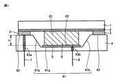
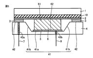
図1に、実施の形態1の窒化物半導体発光装置の模式的な断面図を示す。実施の形態1の窒化物半導体発光装置は、台座4と、台座4上の窒化物半導体発光素子6と、窒化物半導体発光素子6上の透明絶縁板1と、透明絶縁板1の窒化物半導体発光素子6側の表面上に設けられた透明導電膜2とを備えている。
<
[Configuration of nitride semiconductor light emitting device]
FIG. 1 is a schematic cross-sectional view of the nitride semiconductor light emitting device of the first embodiment. The nitride semiconductor light emitting device of the first embodiment includes a
台座4は、台座4の表面中央に凹部41を有している。凹部41は、正方形状の底面41aと、正方形状の底面41aの周縁から斜め上方に延在して底面41aを取り囲むようにして設けられた側面41bとを有している。また、台座4の表面は、凹部41を取り囲むようにして設けられた周縁部42を有している。台座4の周縁部42の表面上には台座4の凹部41を取り囲むようにして第一の電極3が設けられており、台座4の凹部41の底面41a上には第二の電極5が設けられている。なお、底面41aを上方から見たときの底面41aの外形は、特に限定されないが、たとえば、一辺が1.5cmの正方形とすることができる。
The
台座4としては、絶縁性材料を用いることができ、たとえば、絶縁性セラミック、ブラスチックまたはエポキシ樹脂などを用いることができる。また、第一の電極3および第二の電極5としては、たとえば金属などの導電性部材を用いることができる。
As the
窒化物半導体発光素子6は、台座4の凹部41の底面41aの第二の電極5上に設置されている。窒化物半導体発光素子6としては、たとえば、n型GaN層とp型GaN層との積層構造を含む縦型構造の青色発光ダイオードなどを用いることができる。
The nitride semiconductor
本実施の形態においては、窒化物半導体発光素子6として青色発光ダイオードを用いる場合について説明する。本実施の形態において窒化物半導体発光素子6として用いられている青色発光ダイオードは、n型GaN層の下面にn電極が設けられた構成を有し、当該n電極は第二の電極5と電気的に接続されている。また、p型の活性化処理が完了したp型GaN層が上面に露出しており、当該p型GaN層と透明導電膜2とが電気的に接続されている。したがって、本実施の形態で用いられている窒化物半導体発光素子6においては、p型GaN層の上面が第一の電気接続部61となり、n電極の下面が第二の電気接続部62となる。なお、第一の電気接続部61は第一の電極3と導通を図ることができる部材であればよく、第二の電気接続部62は第二の電極5と導通を図ることができる部材であればよい。また、本実施の形態においては、台座4上に1つの青色発光ダイオードのみが設置されているが、台座4上に複数の青色発光ダイオードが設置されてもよい。
In the present embodiment, a case where a blue light emitting diode is used as the nitride semiconductor
透明絶縁板1の窒化物半導体発光素子6側の表面上の透明導電膜2は、台座4の周縁部42上の第一の電極3および窒化物半導体発光素子6の第一の電気接続部61とそれぞれ電気的に接続されている。したがって、第一の電極3は、透明導電膜2を介して、第一の電気接続部61と電気的に接続されていることになる。
The transparent
ここで、透明絶縁板1としては、たとえばサファイア、SiN(窒化珪素)、ガラスまたは石英からなる基板などを用いることができる。また、透明導電膜2としては、たとえばITO(Indium Tin Oxide)を用いることができる。なお、透明導電膜2は、窒化物半導体発光素子6から出射された光の透過率が100%であることが理想であるが、窒化物半導体発光素子6から出射された光の少なくとも一部が透過すればよい。したがって、透明導電膜2における窒化物半導体発光素子6から出射された光の透過率は、たとえば1%以下であってもよい。
Here, as the transparent insulating
また、台座4には貫通孔43aおよび貫通孔43bがそれぞれ設けられている。第一の電極3に電気的に接続する金属リード線7が貫通孔43aを通して外部に引き出されているとともに、第二の電極5に電気的に接続する金属リード線8が貫通孔43bを通して外部に引き出されている。また、第二の電極5の表面から台座4の周縁部42の表面までの鉛直方向の高さhは、たとえば500μmとすることができる。
The
[窒化物半導体発光装置の製造方法]
以下に、実施の形態1の窒化物半導体発光装置の製造方法の一例について説明する。まず、透明絶縁板1として厚さが430μmで、直径が2インチのC面を有するサファイア基板を用意する。ここで、サファイア基板は、両面研磨されていることが好ましい。
[Method for Manufacturing Nitride Semiconductor Light-Emitting Device]
An example of the method for manufacturing the nitride semiconductor light emitting device of the first embodiment will be described below. First, a sapphire substrate having a C surface having a thickness of 430 μm and a diameter of 2 inches is prepared as the transparent insulating
次に、上記のサファイア基板からなる透明絶縁板1の片側の表面上にITOからなる厚さ250nmの透明導電膜2をたとえばスパッタリング法などにより形成する。なお、本実施の形態においては、透明導電膜2としてITOを用いたが、ITOに限定されるものではなく、たとえば、Ni膜とAu膜とが積層した金属薄膜(数オングストロームから数十nm、またそれ以上の厚さでもよい)を用いてもよく、Pt、Pd、CuまたはAgの金属薄膜を用いてもよい。なお、透明導電膜2に金属薄膜を用いる場合の透明導電膜2の厚さは、窒化物半導体発光素子6から出射された光が透過する程度の厚さに調整することが好ましい。
Next, a transparent
次に、透明導電膜2の形成後の透明絶縁板1を台座4の周縁部42の形状に合わせるため、ダイシング装置を用いて1辺が1.5cmの正方形状に成形し、透明絶縁板1の片側の透明導電膜2が台座4を覆うように透明絶縁板1を被せる。このとき、台座4の周縁部42の表面上に設置された第一の電極3と透明導電膜2とが接触し、窒化物半導体発光素子6のp型GaN層が透明導電膜2と接触する。これにより、窒化物半導体発光素子6の上側のp型GaN層が、透明導電膜2を介して、第1の電極3および金属リード線7と電気的に接続される。また、窒化物半導体発光素子6の下側のn型GaN層は、n電極を介して、第2の電極5および金属リード線8と電気的に接続される。なお、窒化物半導体発光素子6は、たとえば有機金属気相成長法などの従来から公知の方法により作製することができる。
Next, in order to match the transparent insulating
また、透明絶縁板1の固定手段は、特に限定されないが、たとえば、樹脂などによって透明絶縁板1を台座4の周縁部42と固定してもよく、台座4の周縁部42にクリップ状の金属などで透明絶縁板1を挟み込むことによって固定してもよい。
The fixing means for the transparent insulating
[窒化物半導体発光装置の評価]
上述のようにして作製した実施の形態1の窒化物半導体発光装置の金属リード線7と金属リード線8との間に電流制御で順方向の駆動電流20mAを印加したところ、金属リード線7と金属リード線8との間の電圧が3.6Vとなり、窒化物半導体発光素子6が青色の発光を呈した。
[Evaluation of nitride semiconductor light emitting device]
When a forward drive current of 20 mA was applied by current control between the
実施の形態1の窒化物半導体発光装置の効果を確認するため、事故等によって実施の形態1の窒化物半導体発光装置の透明絶縁板1が外れることを想定して、セラミックピンセットを用いて透明絶縁板1を台座4から取り外した。これにより、青色の発光を呈していた窒化物半導体発光素子6から青色光は観測されなくなった。また、金属リード線7と金属リード線8との間の電圧は開放となった。
In order to confirm the effect of the nitride semiconductor light emitting device of the first embodiment, it is assumed that the transparent insulating
これは、透明絶縁板1が台座4から外れることによって、透明絶縁板1に形成されていた透明導電膜2も同時に第一の電極3から外れることで駆動電流が遮断され、窒化物半導体発光素子6の動作が停止したためである。
This is because when the transparent insulating
また、比較のため、図11の模式的断面図に示される従来の窒化物半導体発光装置(比較例の窒化物半導体発光装置)を作製した。図11に示す比較例の窒化物半導体発光装置は、透明導電膜2の代わりに金属ワイヤ9を用いて導通を図っている点で実施の形態1の窒化物半導体発光装置と異なっている。
For comparison, a conventional nitride semiconductor light emitting device (a nitride semiconductor light emitting device of a comparative example) shown in the schematic cross-sectional view of FIG. 11 was produced. The nitride semiconductor light emitting device of the comparative example shown in FIG. 11 is different from the nitride semiconductor light emitting device of the first embodiment in that conduction is achieved using a metal wire 9 instead of the transparent
すなわち、比較例の窒化物半導体発光装置においては、窒化物半導体発光素子6の上部の第一の電気接続部61が金属ワイヤ9を介して、第一の電極3に電気的に接続されている。また、第一の電極3は、貫通孔43aを通して台座4の外部に引き出されている金属リード線7と電気的に接続されている。すなわち、窒化物半導体発光素子6の第一の電気接続部61は、金属ワイヤ9および第1の電極3を介して、第1の金属リード7に電気的に接続されている。
That is, in the nitride semiconductor light emitting device of the comparative example, the first
また、実施の形態1の窒化物半導体発光装置と同様に、比較例の窒化物半導体発光装置においても、窒化物半導体発光素子6の下側の第二の電気接続部62は、第2の電極5を介して、貫通孔43bを通して台座4の外部に引き出されている金属リード線8と電気的に接続される。
Similarly to the nitride semiconductor light emitting device of the first embodiment, in the nitride semiconductor light emitting device of the comparative example, the second
比較例の窒化物半導体発光装置の金属リード線7と金属リード線8との間に電流制御で順方向の駆動電流20mAを印加したところ、金属リード線7と金属リード線8との間の電圧が3.6Vとなり、窒化物半導体発光素子6が青色の発光を呈した。しかしながら、セラミックピンセットを用いて、透明絶縁板1を台座4から取り外したが、青色の発光を呈していた窒化物半導体発光素子6からは青色光が出射し続けた。これにより、実施の形態1の窒化物半導体発光装置の効果が確認された。
When a forward drive current of 20 mA is applied between the
[作用効果]
図11に示すように、従来の窒化物半導体発光装置においては、1本または複数本の金属ワイヤ9を用いて窒化物半導体発光素子6に駆動電流を供給することが行なわれている。そのため、従来の窒化物半導体発光装置においては、事故等によって透明絶縁板1が外れた場合でも、窒化物半導体発光素子6の駆動電流の供給回路には何の影響も与えないため、窒化物半導体発光素子6からは光が出射し続けていた。
[Function and effect]
As shown in FIG. 11, in the conventional nitride semiconductor light emitting device, a drive current is supplied to the nitride semiconductor
しかしながら、実施の形態1の窒化物半導体発光装置においては、透明絶縁板1に取り付けられた透明導電膜2が窒化物半導体発光素子6の駆動電流の供給回路に組み込まれているため、事故等によって透明絶縁板1が外れた場合には、透明絶縁板1とともに透明導電膜2が窒化物半導体発光素子6の駆動電流の供給回路から外れる。そのため、実施の形態1の窒化物半導体発光装置においては、窒化物半導体発光素子6が外部に露出した際の窒化物半導体発光素子6への駆動電流の供給を遮断することができる。すなわち、実施の形態1の窒化物半導体発光装置においては、透明絶縁板1と透明導電膜2との接着力が、透明導電膜2と第一の電極3との間の接着力よりも強固であればよい。
However, in the nitride semiconductor light emitting device of the first embodiment, the transparent
[窒化物半導体発光素子のその他の実施形態]
実施の形態1においては、窒化物半導体発光素子6としてp型窒化物半導体層が上側でn型窒化物半導体層が下側の構造を有する青色発光ダイオードを用いる場合について説明したが、これに限定されず、たとえば、n型窒化物半導体層が上側でp型窒化物半導体層が下側の構造を有する青色発光ダイオードを用いてもよい。
[Other Embodiments of Nitride Semiconductor Light-Emitting Device]
In the first embodiment, the case where a blue light emitting diode having a structure in which the p-type nitride semiconductor layer is on the upper side and the n-type nitride semiconductor layer is on the lower side is used as the nitride semiconductor
また、実施の形態1においては、窒化物半導体発光素子6として縦型構造の青色発光ダイオードを用いる場合について説明したが、これに限定されず、たとえば横型構造の青色発光ダイオードを用いてもよい。なお、横型構造の青色発光ダイオードを用いる場合にはたとえば、p型窒化物半導体層に電気的に接続するp電極およびn型窒化物半導体層に電気的に接続するn電極を共に上側とし、p電極およびn電極が短絡しないように、p電極またはn電極のいずれか一方を透明導電膜2と電気的に接続し、他の一方を金属ワイヤ等を用いて第二の電極5に電気的に接続することによって、窒化物半導体発光素子6への駆動電流の供給回路を形成することができる。
In the first embodiment, the case where a vertical blue light emitting diode is used as the nitride semiconductor
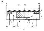
<実施の形態1の変形例>
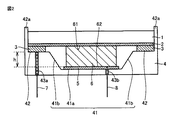
図2に、実施の形態1の窒化物半導体発光装置の変形例の模式的な断面図を示す。図2に示す変形例においては、透明絶縁板1、透明導電膜2および第一の電極3が外部に露出しないように、上方に突出した台座4の周縁部42aを有していることを特徴としている。上方に突出した台座4の周縁部42aにより、透明導電膜2および第一の電極3が外部に露出するのを防止することができることから、透明導電膜2および第一の電極3からの漏電等の電気的な問題の発生を防止することができる。なお、漏電等の電気的な問題の発生を防止する観点からは、上方に突出した台座4の周縁部42aによって、少なくとも透明導電膜2および第一の電極3が外部に露出するのを防止することができればよい。
<Modification of
FIG. 2 is a schematic cross-sectional view of a modification of the nitride semiconductor light emitting device of the first embodiment. In the modification shown in FIG. 2, the transparent insulating
<実施の形態2>
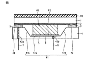
図3に、実施の形態2の窒化物半導体発光装置の模式的な断面図を示す。実施の形態2の窒化物半導体発光装置は、透明絶縁板1の透明導電膜2の設置側とは反対側の表面上に蛍光体板10を備えている点に特徴がある。
<
FIG. 3 is a schematic cross-sectional view of the nitride semiconductor light emitting device of the second embodiment. The nitride semiconductor light emitting device of the second embodiment is characterized in that a
蛍光体板10は、従来から公知の方法で作製される蛍光体を含む板状材であれば特に限定されないが、本実施の形態においては、YAG系蛍光体を含有する1辺が1.5cmの正方形状の表面を有する厚さ500μmの樹脂板を用いている。また、蛍光体板10の固定方法も特に限定されないが、本実施の形態においては、蛍光体板10の周縁に接着材を塗布した後に透明絶縁板1に重ねて固定している。
The
実施の形態2の窒化物半導体発光装置を駆動させるため、実施の形態1の窒化物半導体発光装置と同様にして、金属リード線7と金属リード線8との間に駆動電流20mAを印加したところ、窒化物半導体発光装置の上面からは白色光が観測された。これは、窒化物半導体発光素子6である青色発光ダイオードの光の一部によって蛍光体板10の黄色蛍光体が励起されて黄色の発光を呈するとともに、青色発光ダイオードからの残りの青色光の発光と合成されて白色に見えているためである。実施の形態2においても、台座4上に1つの青色発光ダイオードのみが設置されているが、台座4上に複数の青色発光ダイオードが設置されてもよい。
In order to drive the nitride semiconductor light emitting device of the second embodiment, a driving current of 20 mA is applied between the
また、実施の形態2の窒化物半導体発光装置についても、実施の形態1の窒化物半導体発光装置と同様に、セラミックピンセットを用いて透明絶縁板1を台座4から取り外した。これにより、青色発光ダイオードからの青色光は観測されなくなった。これにより、実施の形態2の窒化物半導体発光装置についても、実施の形態1の窒化物半導体発光装置と同様の作用効果が確認された。
In the nitride semiconductor light emitting device of the second embodiment, the transparent insulating
実施の形態2における上記以外の説明は実施の形態1と同様であるため、ここではその説明については省略する。 Since the description other than the above in the second embodiment is the same as that in the first embodiment, the description thereof is omitted here.
<実施の形態3>
実施の形態3の窒化物半導体発光装置は、窒化物半導体発光素子6として発光波長が365nmの近紫外発光ダイオードを用いていること、および蛍光体板10に含まれる蛍光体としてRGB蛍光体(紫外光によって励起され青色、緑色および赤色の蛍光を呈する蛍光体)を用いていること以外は実施の形態2の窒化物半導体発光装置と同一の構造を有している。なお、実施の形態3の蛍光体板10は、近紫外光が蛍光体板10を通過する間に1/1000の強度まで減衰するように蛍光体板10内の蛍光体濃度が調整されている。
<
In the nitride semiconductor light emitting device of the third embodiment, a near ultraviolet light emitting diode having an emission wavelength of 365 nm is used as the nitride semiconductor
実施の形態3の窒化物半導体発光装置を駆動させるため、金属リード線7と金属リード線8との間に駆動電流60mAを印加したところ、窒化物半導体発光装置の上面からは白色光が観測された。これは、窒化物半導体発光素子6である近紫外発光ダイオードの光によってRGB蛍光体が励起され、青色、緑色および赤色を呈する光がそれぞれ発光したためである。実施の形態3においては、台座4上に1つの近紫外発光ダイオードのみが設置されているが、台座4上に複数の近紫外発光ダイオードが設置されてもよい。
When a drive current of 60 mA was applied between the
また、実施の形態3の窒化物半導体発光装置についても、実施の形態1と同様に、セラミックピンセットを用いて透明絶縁板1を台座4から取り外した。これにより、近紫外発光ダイオードからの近紫外光は観測されなくなった。これにより、実施の形態3の窒化物半導体発光装置についても、実施の形態1の窒化物半導体発光装置と同様の作用効果が確認された。なお、近紫外発光ダイオードからの近紫外光の観測は、安全のため、暗幕で覆われたブース内で、防護ゴーグルを着用し、分光器とマルチチャンネルCCD(Charge Coupled Device)とを用いて行なわれた。
Also, in the nitride semiconductor light emitting device of the third embodiment, the transparent insulating
実施の形態3における上記以外の説明は実施の形態1および実施の形態2と同様であるため、ここではその説明については省略する。 Since the description other than the above in the third embodiment is the same as that in the first and second embodiments, the description thereof is omitted here.
<実施の形態2および実施の形態3の変形例>
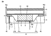
図4に、実施の形態2および実施の形態3の窒化物半導体発光装置の変形例の模式的な断面図を示す。図4に示す変形例においては、透明絶縁板1、透明導電膜2、第一の電極3および蛍光体板10が外部に露出しないように、上方に突出した台座4の周縁部42aを有していることを特徴としている。上方に突出した台座4の周縁部42aにより、透明導電膜2および第一の電極3が外部に露出するのを防止することができることから、透明導電膜2および第一の電極3からの漏電等の電気的な問題の発生を防止することができる。なお、漏電等の電気的な問題の発生を防止する観点からは、上方に突出した台座4の周縁部42aによって、少なくとも透明導電膜2および第一の電極3が外部に露出するのを防止することができればよい。
<Modifications of
FIG. 4 is a schematic cross-sectional view of a modification of the nitride semiconductor light emitting device of the second and third embodiments. In the modification shown in FIG. 4, the transparent insulating
<実施の形態4>
図5に、実施の形態4の窒化物半導体発光装置の模式的な断面図を示す。実施の形態4の窒化物半導体発光装置は、透明絶縁板1と透明導電膜2との間に蛍光体板10を備えていること以外は実施の形態3の窒化物半導体発光装置と同一の構造を有している。すなわち、実施の形態4においても、台座4上に1つの近紫外発光ダイオードのみが設置されていてもよく、複数の近紫外発光ダイオードが設置されていてもよい。
<
FIG. 5 is a schematic cross-sectional view of the nitride semiconductor light emitting device of the fourth embodiment. The nitride semiconductor light emitting device of the fourth embodiment has the same structure as the nitride semiconductor light emitting device of the third embodiment except that the
実施の形態4の窒化物半導体発光装置は、たとえば、透明絶縁板1の下面に予め厚さ500μmの蛍光体板10を形成しておき、その後、実施の形態1と同様にして、蛍光体板10上に透明導電膜2を形成することによって作製することができる。
In the nitride semiconductor light emitting device of the fourth embodiment, for example, a
実施の形態4の窒化物半導体発光装置についても実施の形態3の窒化物半導体発光装置と同様にして作用効果の確認をしたところ、実施の形態3の窒化物半導体発光装置と同様の作用効果が確認された。すなわち、実施の形態4の窒化物半導体発光装置においては、透明導電膜2と蛍光体板10との接着力が、透明導電膜2と第一の電極3との間の接着力よりも強固であればよい。
The effect of the nitride semiconductor light emitting device of the fourth embodiment was also confirmed in the same manner as the nitride semiconductor light emitting device of the third embodiment. As a result, the same effect as the nitride semiconductor light emitting device of the third embodiment was obtained. confirmed. That is, in the nitride semiconductor light emitting device of the fourth embodiment, the adhesive force between the transparent
実施の形態4における上記以外の説明は実施の形態1〜実施の形態3と同様であるためここではその説明については省略する。 Since the description other than the above in the fourth embodiment is the same as that in the first to third embodiments, the description thereof is omitted here.
<実施の形態5>
図6に、実施の形態5の窒化物半導体発光装置の模式的な断面図を示す。実施の形態5の窒化物半導体発光装置は、蛍光体板10の代わりに、透明絶縁板1中にRGB蛍光体11を分散させていること以外は実施の形態3の窒化物半導体発光装置と同一の構造を有している。すなわち、実施の形態5においても、台座4上に1つの近紫外発光ダイオードのみが設置されていてもよく、複数の近紫外発光ダイオードが設置されていてもよい。
<
FIG. 6 is a schematic cross-sectional view of the nitride semiconductor light emitting device of the fifth embodiment. The nitride semiconductor light-emitting device of the fifth embodiment is the same as the nitride semiconductor light-emitting device of the third embodiment except that the
RGB蛍光体11を分散させた透明絶縁板1は、たとえば、実施の形態2〜実施の形態4の蛍光体板10と同様にして作製することができる。
The transparent insulating
実施の形態5の窒化物半導体発光装置についても実施の形態3の窒化物半導体発光装置と同様にして作用効果の確認をしたところ、実施の形態3の窒化物半導体発光装置と同様の作用効果が確認された。 With respect to the nitride semiconductor light emitting device of the fifth embodiment, the effects were confirmed in the same manner as the nitride semiconductor light emitting device of the third embodiment. As a result, the same effects as the nitride semiconductor light emitting device of the third embodiment were obtained. confirmed.
実施の形態5における上記以外の説明は実施の形態1〜実施の形態4と同様であるためここではその説明については省略する。 Since the description other than the above in the fifth embodiment is the same as that in the first to fourth embodiments, the description thereof is omitted here.
<実施の形態6>
実施の形態6の窒化物半導体発光装置は、窒化物半導体発光素子6として青色発光ダイオード素子を用い、蛍光体板10として黄色蛍光体を含む蛍光体板を用いたこと以外は実施の形態4の窒化物半導体発光装置と同一の構造を有している。すなわち、実施の形態6においても、台座4上に1つの近紫外発光ダイオードのみが設置されていてもよく、複数の近紫外発光ダイオードが設置されていてもよい。
<
The nitride semiconductor light emitting device of the sixth embodiment is the same as that of the fourth embodiment except that a blue light emitting diode element is used as the nitride semiconductor
実施の形態6の窒化物半導体発光装置についても実施の形態3の窒化物半導体発光装置と同様にして作用効果の確認をしたところ、実施の形態3の窒化物半導体発光装置と同様の作用効果が確認された。 The effect of the nitride semiconductor light emitting device of the sixth embodiment was also confirmed in the same manner as the nitride semiconductor light emitting device of the third embodiment. As a result, the same effect as the nitride semiconductor light emitting device of the third embodiment was obtained. confirmed.
実施の形態6における上記以外の説明は実施の形態1〜実施の形態5と同様であるためここではその説明については省略する。 Since the description other than the above in the sixth embodiment is the same as that in the first to fifth embodiments, the description thereof is omitted here.
<実施の形態7>
実施の形態7の窒化物半導体発光装置は、窒化物半導体発光素子6として青色発光ダイオード素子を用い、透明絶縁板1がRGB蛍光体の代わりに黄色蛍光体を含むこと以外は実施の形態5の窒化物半導体発光装置と同一の構造を有している。すなわち、実施の形態7においても、台座4上に1つの近紫外発光ダイオードのみが設置されていてもよく、複数の近紫外発光ダイオードが設置されていてもよい。
<
The nitride semiconductor light emitting device of the seventh embodiment uses a blue light emitting diode element as the nitride semiconductor
実施の形態7の窒化物半導体発光装置についても実施の形態3の窒化物半導体発光装置と同様にして作用効果の確認をしたところ、実施の形態3の窒化物半導体発光装置と同様の作用効果が確認された。 As for the nitride semiconductor light emitting device of the seventh embodiment, the operational effects were confirmed in the same manner as the nitride semiconductor light emitting device of the third embodiment, and the same operational effects as the nitride semiconductor light emitting device of the third embodiment were obtained. confirmed.
実施の形態7における上記以外の説明は実施の形態1〜実施の形態6と同様であるためここではその説明については省略する。 Since the description other than the above in the seventh embodiment is the same as that in the first to sixth embodiments, the description thereof is omitted here.
<実施の形態4および実施の形態6の変形例>
図7に、実施の形態4および実施の形態6の窒化物半導体発光装置の変形例の模式的な断面図を示す。図7に示す変形例においては、透明絶縁板1、透明導電膜2、第一の電極3および蛍光体板10が外部に露出しないように、上方に突出した台座4の周縁部42aを有していることを特徴としている。上方に突出した台座4の周縁部42aにより、透明導電膜2および第一の電極3が外部に露出するのを防止することができることから、透明導電膜2および第一の電極3からの漏電等の電気的な問題の発生を防止することができる。なお、漏電等の電気的な問題の発生を防止する観点からは、上方に突出した台座4の周縁部42aによって、少なくとも透明導電膜2および第一の電極3が外部に露出するのを防止することができればよい。
<Modification of
FIG. 7 is a schematic cross-sectional view of a modification of the nitride semiconductor light emitting device of the fourth and sixth embodiments. In the modification shown in FIG. 7, the transparent insulating
<実施の形態5および実施の形態7の変形例>
図8に、実施の形態5および実施の形態7の窒化物半導体発光装置の変形例の模式的な断面図を示す。図8に示す変形例においては、透明絶縁板1、透明導電膜2および第一の電極3が外部に露出しないように、上方に突出した台座4の周縁部42aを有していることを特徴としている。上方に突出した台座4の周縁部42aにより、透明導電膜2および第一の電極3が外部に露出するのを防止することができることから、透明導電膜2および第一の電極3からの漏電等の電気的な問題の発生を防止することができる。なお、漏電等の電気的な問題の発生を防止する観点からは、上方に突出した台座4の周縁部42aによって、少なくとも透明導電膜2および第一の電極3が外部に露出するのを防止することができればよい。
<Modification of
FIG. 8 is a schematic cross-sectional view of a modification of the nitride semiconductor light emitting device of the fifth and seventh embodiments. In the modification shown in FIG. 8, the transparent insulating
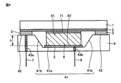
<実施の形態8>
図9に、実施の形態8の窒化物半導体発光装置の模式的な断面図を示す。実施の形態8の窒化物半導体発光装置は、窒化物半導体発光素子6としての青色発光ダイオードの上側のp型GaN層上に接続用電極71を設置し、接続用電極71と透明導電膜2とを接触させていること以外は実施の形態1の窒化物半導体発光装置と同一の構造を有している。この場合に、窒化物半導体発光素子6の第一の電気接続部61は、接続用電極71と接続されているp型GaN層の表面となる。
<Eighth embodiment>
FIG. 9 is a schematic cross-sectional view of the nitride semiconductor light emitting device of the eighth embodiment. In the nitride semiconductor light emitting device of the eighth embodiment, a
実施の形態8の窒化物半導体発光装置についても実施の形態1の窒化物半導体発光装置と同様にして作用効果の確認をしたところ、実施の形態1の窒化物半導体発光装置と同様の作用効果が確認された。 As for the nitride semiconductor light emitting device of the eighth embodiment, the effects were confirmed in the same manner as the nitride semiconductor light emitting device of the first embodiment. As a result, the same effects as the nitride semiconductor light emitting device of the first embodiment were obtained. confirmed.
また、実施の形態2〜実施の形態7の窒化物半導体発光装置においても、実施の形態8の窒化物半導体発光装置と同様に、窒化物半導体発光素子6としての青色発光ダイオードの上側のp型GaN層上に接続用電極71を設置して、実施の形態8の窒化物半導体発光装置と同様にして作用効果の確認をしたところ、実施の形態8の窒化物半導体発光装置と同様の作用効果が確認された。
Also in the nitride semiconductor light emitting devices of the second to seventh embodiments, similarly to the nitride semiconductor light emitting device of the eighth embodiment, the p-type above the blue light emitting diode as the nitride semiconductor
なお、接続用電極71は、たとえば、透明導電膜2と同様の材質からなる透明電極であってもよい。また、実施の形態8においても、台座4上に1つの青色発光ダイオードのみが設置されていてもよく、複数の青色発光ダイオードが設置されていてもよい。
The
実施の形態8における上記以外の説明は実施の形態1〜実施の形態7と同様であるためここではその説明については省略する。 Since the description other than the above in the eighth embodiment is the same as that in the first to seventh embodiments, the description thereof is omitted here.
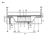
<実施の形態8の変形例>
図10に、実施の形態8の窒化物半導体発光装置の変形例の模式的な断面図を示す。図10に示す変形例においては、透明絶縁板1、透明導電膜2および第一の電極3が外部に露出しないように、上方に突出した台座4の周縁部42aを有していることを特徴としている。上方に突出した台座4の周縁部42aにより、透明導電膜2および第一の電極3が外部に露出するのを防止することができることから、透明導電膜2および第一の電極3からの漏電等の電気的な問題の発生を防止することができる。なお、漏電等の電気的な問題の発生を防止する観点からは、上方に突出した台座4の周縁部42aによって、少なくとも透明導電膜2および第一の電極3が外部に露出するのを防止することができればよい。
<Modification of
FIG. 10 is a schematic cross-sectional view of a modification of the nitride semiconductor light emitting device of the eighth embodiment. In the modification shown in FIG. 10, the
<実施の形態9>
実施の形態9の窒化物半導体発光装置は、実施の形態1〜実施の形態8の窒化物半導体発光装置の透明導電膜2にグラフェンを用いたことを特徴としている。実施の形態9の窒化物半導体発光装置についても実施の形態1〜実施の形態8の窒化物半導体発光装置と同様にして作用効果を確認したところ、実施の形態1〜実施の形態8の窒化物半導体発光装置と同様の作用効果が確認された。また、実施の形態9においても、台座4上に1つの発光ダイオードのみが設置されていてもよく、複数の発光ダイオードが設置されていてもよい。
<Embodiment 9>
The nitride semiconductor light emitting device of the ninth embodiment is characterized in that graphene is used for the transparent
グラフェンは炭素原子がsp2混成軌道によるσ結合で2次元的(x−y平面とする)に配列したものであり、残りのpz軌道によるπ電子は面内に自由度がある。透明導電膜2を構成するグラフェンからなる層は単層または複数層のいずれであってもよい。
Graphene is a two-dimensional (xy plane) arrangement of carbon atoms with σ bonds by sp2 hybrid orbitals, and the remaining π electrons by pz orbitals have a degree of freedom in the plane. The layer made of graphene constituting the transparent
透明導電膜2の材質としては、窒化物半導体発光素子6から出射される光に対する透過率が高い材料を用いることが好ましいため、以下に、グラフェン、ITOおよびその他の金属の透過率および熱特性に関して説明する。
As the material of the transparent
グラフェンは単層でエネルギーと波数kの関係が線形でバンドギャップを持たない。この特異なバンド構造によりグラフェンでは面内のキャリア移動度が10000〜200000cm2/Vsと言われている。これは、グラフェンの面内におけるキャリア移動度が高く、飽和電流密度が他の半導体に比べて大きく、電流が流れやすいことを意味する。そのため、グラフェンは、1層〜数層で十分であると考えられる。 Graphene is a single layer, and the relationship between energy and wave number k is linear and has no band gap. Due to this unique band structure, in-plane carrier mobility is said to be 10,000 to 200,000 cm 2 / Vs in graphene. This means that the carrier mobility in the surface of graphene is high, the saturation current density is larger than that of other semiconductors, and the current flows easily. Therefore, it is considered that one to several layers of graphene are sufficient.
[透過率]
グラフェンの1層当たりの光の吸収率は、赤外、可視および紫外域までの波長域においては、光の波長によらず2.3%と一定の値をとり、残りの光は透過する。一方、ITOは、3.75eVのバンドギャップ(波長330nmの光のエネルギーに相当)を有するため、膜厚にもよるが、一般的に実用的な厚さで、可視域でおよそ80%以上の透過率を有するように設計されるが、波長200nm台の深紫外と呼ばれる波長域では吸収が顕著になり、透過率が極端に低くなる。また、その他の金属においても、一般的に自由電子の高いプラズマ周波数により可視から近紫外に至るまで反射率が高く、また、深紫外では吸収率が高くなる。したがって、グラフェンは、光の波長を問わずに高い透過率を発現することができるため、ITOやその他の金属と比べて、透明導電膜2の材料としては好ましい特性を有していると考えられる。
[Transmissivity]
The absorption rate of light per layer of graphene has a constant value of 2.3% regardless of the wavelength of light in the infrared, visible, and ultraviolet wavelength ranges, and the remaining light is transmitted. On the other hand, since ITO has a band gap of 3.75 eV (corresponding to the energy of light having a wavelength of 330 nm), although it depends on the film thickness, it is generally a practical thickness and approximately 80% or more in the visible region. Although it is designed to have transmittance, absorption becomes remarkable in a wavelength region called deep ultraviolet having a wavelength of about 200 nm, and the transmittance becomes extremely low. In addition, other metals generally have a high reflectance from the visible to the near ultraviolet due to a high plasma frequency of free electrons, and an absorptivity in the deep ultraviolet. Therefore, since graphene can express a high transmittance regardless of the wavelength of light, it is considered that the graphene has preferable characteristics as a material of the transparent
[熱特性]
グラフェンの熱伝導率は5000W/m/K以上とであり、ITOの熱伝導率はおよそ80W/m/Kであり、Auの熱伝導率はおよそ320W/m/Kである。また、透明絶縁板1に用いられたサファイアの熱伝導率およそ40W/m/Kであり、ガラスの熱伝導率は1W/m/Kである。
[Thermal characteristics]
The thermal conductivity of graphene is 5000 W / m / K or more, the thermal conductivity of ITO is about 80 W / m / K, and the thermal conductivity of Au is about 320 W / m / K. The thermal conductivity of sapphire used for the transparent insulating
したがって、窒化物半導体発光素子6は少なからず熱を放出するが、透明導電膜2にグラフェンを用いることによってその熱を排出することができ、窒化物半導体発光装置の信頼性を向上させることができる。
Therefore, the nitride semiconductor
グラフェンの製法としては、たとえば、グラファイトからの剥離(スコッチテープ法)、SiCエピタキシャル成長層の真空熱分解、または金属触媒による化学気相成長法等が挙げられるが、グラフェンの製法は特に限定されない。 Examples of the method for producing graphene include exfoliation from graphite (Scotch tape method), vacuum pyrolysis of a SiC epitaxial growth layer, or chemical vapor deposition using a metal catalyst, but the method for producing graphene is not particularly limited.
また、グラフェン以外にも、グラフェンが複数積層した構造であるグラファイトカーボンナノチューブ、またはグラフェン、グラファイトおよびカーボンナノチューブからなる群から選択された2種以上の複合体を透明導電膜2としても用いた場合にも、実施の形態1〜実施の形態9の窒化物半導体発光装置と同様の作用効果を確認することができる。
In addition to graphene, when the transparent
また、実施の形態1〜実施の形態9の窒化物半導体発光装置の透明導電膜2として、AlN(窒化アルミニウム)、AlGaN(窒化アルミニウムガリウム)、AlInGaN(窒化アルミニウムインジウムガリウム)、InGaN(窒化インジウムガリウム)、GaN(窒化ガリウム)、InN(窒化インジウム)、ITO、ZnO(酸化亜鉛)、MgZnO(酸化マグネシウム亜鉛)およびIGZO(酸化インジウムガリウム亜鉛)からなる群から選択された少なくとも1種を含む材料を用いた場合にも、実施の形態1〜実施の形態9の窒化物半導体発光装置と同様の作用効果を確認することができる。
Further, as the transparent
<付記>
(1)本発明の実施態様によれば、台座と、台座上の窒化物半導体発光素子と、窒化物半導体発光素子上の透明絶縁板と、台座上の第一の電極と第二の電極と、透明絶縁板の窒化物半導体発光素子側の表面上に設けられた透明導電膜とを備え、窒化物半導体発光素子は第一の電気接続部と第二の電気接続部とを有し、第一の電極は透明導電膜を介して第一の電気接続部と電気的に接続されており、第二の電極は第二の電気接続部と電気的に接続されてなる窒化物半導体発光装置を提供することができる。このような構成とすることにより、透明絶縁板に設けられた透明導電膜が窒化物半導体発光素子の駆動電流の供給回路に組み込まれているため、事故等によって透明絶縁板が外れた場合には、透明絶縁板とともに透明導電膜が窒化物半導体発光素子の駆動電流の供給回路から外すことができる。そのため、窒化物半導体発光素子が外部に露出した際の窒化物半導体発光素子への駆動電流の供給を遮断することができる。
<Appendix>
(1) According to an embodiment of the present invention, a base, a nitride semiconductor light emitting element on the base, a transparent insulating plate on the nitride semiconductor light emitting element, a first electrode and a second electrode on the base, A transparent conductive film provided on the surface of the transparent insulating plate on the nitride semiconductor light emitting element side, the nitride semiconductor light emitting element having a first electrical connection portion and a second electrical connection portion, One electrode is electrically connected to the first electrical connection portion through a transparent conductive film, and the second electrode is a nitride semiconductor light emitting device electrically connected to the second electrical connection portion. Can be provided. By adopting such a configuration, the transparent conductive film provided on the transparent insulating plate is incorporated in the drive current supply circuit of the nitride semiconductor light-emitting element, so when the transparent insulating plate is removed due to an accident or the like. The transparent conductive film together with the transparent insulating plate can be removed from the drive current supply circuit of the nitride semiconductor light emitting device. Therefore, it is possible to cut off the supply of drive current to the nitride semiconductor light emitting device when the nitride semiconductor light emitting device is exposed to the outside.
(2)本発明の実施態様の窒化物半導体発光装置は、透明絶縁板の窒化物半導体発光素子側の表面とは反対側の表面上、透明絶縁板と透明導電膜との間、および透明絶縁板の内部からなる群から選択された少なくとも1箇所に、窒化物半導体発光素子より出射される光により励起され可視光を発光する蛍光体を備えていてもよい。この場合には、本発明の実施態様の窒化物半導体発光装置から、様々な種類の色の光を発光させることが可能となる。 (2) A nitride semiconductor light emitting device according to an embodiment of the present invention includes a transparent insulating plate on a surface opposite to the nitride semiconductor light emitting element side surface, between the transparent insulating plate and the transparent conductive film, and transparent insulation. A phosphor that emits visible light when excited by light emitted from the nitride semiconductor light emitting element may be provided at at least one location selected from the group consisting of the inside of the plate. In this case, light of various types can be emitted from the nitride semiconductor light emitting device according to the embodiment of the present invention.
(3)本発明の実施態様の窒化物半導体発光装置においては、窒化物半導体発光素子に接続用電極が設けられており、透明導電膜と接続用電極とが電気的に接続されていてもよい。この場合にも、窒化物半導体発光素子が外部に露出した際の窒化物半導体発光素子への駆動電流の供給を遮断することができるという作用効果を発現させることができる。 (3) In the nitride semiconductor light emitting device according to the embodiment of the present invention, the nitride semiconductor light emitting element may be provided with a connection electrode, and the transparent conductive film and the connection electrode may be electrically connected. . Also in this case, it is possible to exhibit an effect that the supply of drive current to the nitride semiconductor light emitting device when the nitride semiconductor light emitting device is exposed to the outside can be cut off.
(4)本発明の実施態様の窒化物半導体発光装置において、透明導電膜は、グラファイト、グラフェンおよびカーボンナノチューブからなる群から選択された少なくとも1種を含んでいてもよい。この場合にも、窒化物半導体発光素子が外部に露出した際の窒化物半導体発光素子への駆動電流の供給を遮断することができるという作用効果を発現させることができる。 (4) In the nitride semiconductor light emitting device of the embodiment of the present invention, the transparent conductive film may contain at least one selected from the group consisting of graphite, graphene, and carbon nanotubes. Also in this case, it is possible to exhibit an effect that the supply of drive current to the nitride semiconductor light emitting device when the nitride semiconductor light emitting device is exposed to the outside can be cut off.
(5)本発明の実施態様の窒化物半導体発光装置において、透明導電膜は、AlN、AlGaN、AlInGaN、InGaN、GaN、InN、ITO、ZnO、MgZnOおよびIGZOからなる群から選択された少なくとも1種を含んでいてもよい。この場合にも、窒化物半導体発光素子が外部に露出した際の窒化物半導体発光素子への駆動電流の供給を遮断することができるという作用効果を発現させることができる。 (5) In the nitride semiconductor light emitting device of the embodiment of the present invention, the transparent conductive film is at least one selected from the group consisting of AlN, AlGaN, AlInGaN, InGaN, GaN, InN, ITO, ZnO, MgZnO, and IGZO. May be included. Also in this case, it is possible to exhibit an effect that the supply of drive current to the nitride semiconductor light emitting device when the nitride semiconductor light emitting device is exposed to the outside can be cut off.
以上のように本発明の実施の形態について説明を行なったが、上述の各実施の形態の構成を適宜組み合わせることも当初から予定している。 As described above, the embodiments of the present invention have been described, but it is also planned from the beginning to appropriately combine the configurations of the above-described embodiments.
今回開示された実施の形態はすべての点で例示であって制限的なものではないと考えられるべきである。本発明の範囲は上記した説明ではなくて特許請求の範囲によって示され、特許請求の範囲と均等の意味および範囲内でのすべての変更が含まれることが意図される。 The embodiment disclosed this time should be considered as illustrative in all points and not restrictive. The scope of the present invention is defined by the terms of the claims, rather than the description above, and is intended to include any modifications within the scope and meaning equivalent to the terms of the claims.
本発明は、窒化物半導体発光装置に利用することができ、特に照明用光源としての窒化物半導体発光装置に好適に利用することができる。 The present invention can be used for a nitride semiconductor light-emitting device, and can be particularly suitably used for a nitride semiconductor light-emitting device as an illumination light source.
1 透明絶縁板、2 透明導電膜、3 第一の電極、4 台座、5 第二の電極、6 窒化物半導体発光素子、7,8 金属リード線、9 金属ワイヤ、10 蛍光体板、11 蛍光体、41 凹部、41a 凹部の底面、41b 凹部の側面、42,42a 周縁部、43a,43b 貫通孔、61 第一の電気接続部、62 第二の電気接続部。
DESCRIPTION OF
Claims (5)
前記台座上の窒化物半導体発光素子と、
前記窒化物半導体発光素子上の透明絶縁板と、
前記台座上の第一の電極と第二の電極と、
前記透明絶縁板の前記窒化物半導体発光素子側の表面上に設けられた透明導電膜と、を備え、
前記窒化物半導体発光素子は、第一の電気接続部と第二の電気接続部とを有し、
前記第一の電極は、前記透明導電膜を介して、前記第一の電気接続部と電気的に接続されており、
前記第二の電極は、前記第二の電気接続部と電気的に接続されてなる、窒化物半導体発光装置。 A pedestal,
A nitride semiconductor light emitting device on the pedestal;
A transparent insulating plate on the nitride semiconductor light emitting device;
A first electrode and a second electrode on the pedestal;
A transparent conductive film provided on the surface of the transparent insulating plate on the nitride semiconductor light emitting element side, and
The nitride semiconductor light emitting device has a first electrical connection portion and a second electrical connection portion,
The first electrode is electrically connected to the first electrical connection portion via the transparent conductive film,
The nitride semiconductor light emitting device, wherein the second electrode is electrically connected to the second electrical connection portion.
前記透明導電膜と前記接続用電極とが電気的に接続されてなる、請求項1または請求項2に記載の窒化物半導体発光装置。 A connection electrode is provided on the nitride semiconductor light emitting device,
The nitride semiconductor light-emitting device according to claim 1, wherein the transparent conductive film and the connection electrode are electrically connected.
Priority Applications (1)
| Application Number | Priority Date | Filing Date | Title |
|---|---|---|---|
| JP2013251044A JP6312412B2 (en) | 2013-12-04 | 2013-12-04 | Nitride semiconductor light emitting device |
Applications Claiming Priority (1)
| Application Number | Priority Date | Filing Date | Title |
|---|---|---|---|
| JP2013251044A JP6312412B2 (en) | 2013-12-04 | 2013-12-04 | Nitride semiconductor light emitting device |
Publications (2)
| Publication Number | Publication Date |
|---|---|
| JP2015109331A true JP2015109331A (en) | 2015-06-11 |
| JP6312412B2 JP6312412B2 (en) | 2018-04-18 |
Family
ID=53439498
Family Applications (1)
| Application Number | Title | Priority Date | Filing Date |
|---|---|---|---|
| JP2013251044A Expired - Fee Related JP6312412B2 (en) | 2013-12-04 | 2013-12-04 | Nitride semiconductor light emitting device |
Country Status (1)
| Country | Link |
|---|---|
| JP (1) | JP6312412B2 (en) |
Cited By (4)
| Publication number | Priority date | Publication date | Assignee | Title |
|---|---|---|---|---|
| CN110581111A (en) * | 2018-06-11 | 2019-12-17 | 海华科技股份有限公司 | support, optical assembly and optical module |
| CN110579849A (en) * | 2018-06-11 | 2019-12-17 | 海华科技股份有限公司 | Optical element, optical module and optical module |
| JP2020080400A (en) * | 2018-11-13 | 2020-05-28 | 株式会社ダイセル | Optical member, laser module and laser device including optical member |
| JP2021506108A (en) * | 2017-12-04 | 2021-02-18 | トンシュー グループ カンパニー リミテッドTunghsu Group Co., Ltd. | Top board for micro LED devices, micro LED devices and micro LED display devices |
Citations (13)
| Publication number | Priority date | Publication date | Assignee | Title |
|---|---|---|---|---|
| JPH0317656U (en) * | 1989-06-30 | 1991-02-21 | ||
| JP2004172578A (en) * | 2002-09-02 | 2004-06-17 | Matsushita Electric Ind Co Ltd | Light-emitting device |
| JP2007207895A (en) * | 2006-01-31 | 2007-08-16 | Kyocera Corp | Light emitting device and light emitting module |
| US20090173954A1 (en) * | 2008-01-03 | 2009-07-09 | Goldeneye, Inc. | Semiconducting sheet |
| JP2011513925A (en) * | 2008-03-07 | 2011-04-28 | オスラム オプト セミコンダクターズ ゲゼルシャフト ミット ベシュレンクテル ハフツング | Optoelectronic element |
| US20110163298A1 (en) * | 2010-01-04 | 2011-07-07 | Chien-Min Sung | Graphene and Hexagonal Boron Nitride Devices |
| JP2011135072A (en) * | 2009-12-22 | 2011-07-07 | Lg Innotek Co Ltd | Light-emitting element, light-emitting element package, and lighting system |
| JP2011176045A (en) * | 2010-02-23 | 2011-09-08 | Fujifilm Corp | Laminated type semiconductor light-emitting element |
| JP2011211014A (en) * | 2010-03-30 | 2011-10-20 | Sony Corp | Light emitting element, display device, display method, and electronic apparatus |
| JP2011243666A (en) * | 2010-05-14 | 2011-12-01 | Fuji Mach Mfg Co Ltd | Light emitting device mounting method and light emitting device mounting structure |
| US20120088319A1 (en) * | 2010-10-08 | 2012-04-12 | Veerasamy Vijayen S | Light source with hybrid coating, device including light source with hybrid coating, and/or methods of making the same |
| JP2013531378A (en) * | 2010-06-29 | 2013-08-01 | クーレッジ ライティング インコーポレイテッド | Electronic device with flexible substrate |
| JP2013536592A (en) * | 2010-08-27 | 2013-09-19 | クォークスター・エルエルシー | Solid light sheet or strip for general lighting |
-
2013
- 2013-12-04 JP JP2013251044A patent/JP6312412B2/en not_active Expired - Fee Related
Patent Citations (13)
| Publication number | Priority date | Publication date | Assignee | Title |
|---|---|---|---|---|
| JPH0317656U (en) * | 1989-06-30 | 1991-02-21 | ||
| JP2004172578A (en) * | 2002-09-02 | 2004-06-17 | Matsushita Electric Ind Co Ltd | Light-emitting device |
| JP2007207895A (en) * | 2006-01-31 | 2007-08-16 | Kyocera Corp | Light emitting device and light emitting module |
| US20090173954A1 (en) * | 2008-01-03 | 2009-07-09 | Goldeneye, Inc. | Semiconducting sheet |
| JP2011513925A (en) * | 2008-03-07 | 2011-04-28 | オスラム オプト セミコンダクターズ ゲゼルシャフト ミット ベシュレンクテル ハフツング | Optoelectronic element |
| JP2011135072A (en) * | 2009-12-22 | 2011-07-07 | Lg Innotek Co Ltd | Light-emitting element, light-emitting element package, and lighting system |
| US20110163298A1 (en) * | 2010-01-04 | 2011-07-07 | Chien-Min Sung | Graphene and Hexagonal Boron Nitride Devices |
| JP2011176045A (en) * | 2010-02-23 | 2011-09-08 | Fujifilm Corp | Laminated type semiconductor light-emitting element |
| JP2011211014A (en) * | 2010-03-30 | 2011-10-20 | Sony Corp | Light emitting element, display device, display method, and electronic apparatus |
| JP2011243666A (en) * | 2010-05-14 | 2011-12-01 | Fuji Mach Mfg Co Ltd | Light emitting device mounting method and light emitting device mounting structure |
| JP2013531378A (en) * | 2010-06-29 | 2013-08-01 | クーレッジ ライティング インコーポレイテッド | Electronic device with flexible substrate |
| JP2013536592A (en) * | 2010-08-27 | 2013-09-19 | クォークスター・エルエルシー | Solid light sheet or strip for general lighting |
| US20120088319A1 (en) * | 2010-10-08 | 2012-04-12 | Veerasamy Vijayen S | Light source with hybrid coating, device including light source with hybrid coating, and/or methods of making the same |
Cited By (10)
| Publication number | Priority date | Publication date | Assignee | Title |
|---|---|---|---|---|
| JP2021506108A (en) * | 2017-12-04 | 2021-02-18 | トンシュー グループ カンパニー リミテッドTunghsu Group Co., Ltd. | Top board for micro LED devices, micro LED devices and micro LED display devices |
| US11545607B2 (en) | 2017-12-04 | 2023-01-03 | Tunghsu Group Co., Ltd. | Upper substrate for miniature LED component, miniature LED component, and miniature LED display device |
| CN110581111A (en) * | 2018-06-11 | 2019-12-17 | 海华科技股份有限公司 | support, optical assembly and optical module |
| CN110579849A (en) * | 2018-06-11 | 2019-12-17 | 海华科技股份有限公司 | Optical element, optical module and optical module |
| JP2019216227A (en) * | 2018-06-11 | 2019-12-19 | 海華科技股▲分▼有限公司 | Retainer, optical component and optical module |
| JP2019216226A (en) * | 2018-06-11 | 2019-12-19 | 海華科技股▲分▼有限公司 | Optical element, optical component an optical module |
| US10763375B2 (en) | 2018-06-11 | 2020-09-01 | Azurewave Technologies, Inc. | Optical assembly and optical module |
| JP2020080400A (en) * | 2018-11-13 | 2020-05-28 | 株式会社ダイセル | Optical member, laser module and laser device including optical member |
| JP2021132230A (en) * | 2018-11-13 | 2021-09-09 | 株式会社ダイセル | Optical member, laser module and laser device including optical member |
| JP7119171B2 (en) | 2018-11-13 | 2022-08-16 | 株式会社ダイセル | OPTICAL MEMBER, LASER MODULE AND LASER DEVICE INCLUDING THE OPTICAL MEMBER |
Also Published As
| Publication number | Publication date |
|---|---|
| JP6312412B2 (en) | 2018-04-18 |
Similar Documents
| Publication | Publication Date | Title |
|---|---|---|
| JP5535114B2 (en) | Light emitting device, light emitting module, and method of manufacturing light emitting device | |
| JP5657591B2 (en) | Semiconductor light emitting device and manufacturing method thereof | |
| KR101276053B1 (en) | Semiconductor light emitting device and light emitting apparatus | |
| JP2015191911A (en) | Semiconductor light emitting device | |
| JP2008227553A (en) | Semiconductor light-emitting device and manufacturing method thereof | |
| TWI699011B (en) | Semiconductor light emitting device | |
| JP2014003283A (en) | Semiconductor light-emitting device and light source unit | |
| JP2008210900A (en) | Semiconductor light emitting element and light emitting device provided with the same | |
| US10516080B2 (en) | Semiconductor device and apparatus for improved light emission | |
| JP5503572B2 (en) | Light emitting element | |
| US20140077153A1 (en) | Photonic Devices with Embedded Hole Injection Layer to Improve Efficiency and Droop Rate | |
| JP2013232479A (en) | Semiconductor light-emitting device | |
| JP2011249411A (en) | Semiconductor light-emitting element, light-emitting device, illumination device, display device, signal light unit and road information device | |
| EP2533312B1 (en) | Light-emitting diode package | |
| JP6312412B2 (en) | Nitride semiconductor light emitting device | |
| TWI500186B (en) | Wavelength converter and semiconductor light emitting device | |
| US8648375B2 (en) | Semiconductor light emitting device and light emitting module | |
| JP2015176963A (en) | Semiconductor light emitting device | |
| JP6385680B2 (en) | Light emitting element | |
| JP5518273B1 (en) | Light emitting diode element and light emitting diode device | |
| CN106159073B (en) | Light emitting element and method for manufacturing the same | |
| KR20140023512A (en) | Nitride light emitting device | |
| US8173469B2 (en) | Fabrication method of light emitting device | |
| KR100887072B1 (en) | Semiconductor light emitting device and semiconductor light emitting device package using the same | |
| JP2005268775A (en) | Semiconductor light emitting element and its manufacturing method |
Legal Events
| Date | Code | Title | Description |
|---|---|---|---|
| A621 | Written request for application examination |
Free format text: JAPANESE INTERMEDIATE CODE: A621 Effective date: 20160923 |
|
| A977 | Report on retrieval |
Free format text: JAPANESE INTERMEDIATE CODE: A971007 Effective date: 20170524 |
|
| A131 | Notification of reasons for refusal |
Free format text: JAPANESE INTERMEDIATE CODE: A131 Effective date: 20170606 |
|
| A521 | Request for written amendment filed |
Free format text: JAPANESE INTERMEDIATE CODE: A523 Effective date: 20170803 |
|
| A131 | Notification of reasons for refusal |
Free format text: JAPANESE INTERMEDIATE CODE: A131 Effective date: 20171205 |
|
| A521 | Request for written amendment filed |
Free format text: JAPANESE INTERMEDIATE CODE: A523 Effective date: 20171214 |
|
| TRDD | Decision of grant or rejection written | ||
| A01 | Written decision to grant a patent or to grant a registration (utility model) |
Free format text: JAPANESE INTERMEDIATE CODE: A01 Effective date: 20180306 |
|
| A61 | First payment of annual fees (during grant procedure) |
Free format text: JAPANESE INTERMEDIATE CODE: A61 Effective date: 20180320 |
|
| R150 | Certificate of patent or registration of utility model |
Ref document number: 6312412 Country of ref document: JP Free format text: JAPANESE INTERMEDIATE CODE: R150 |
|
| LAPS | Cancellation because of no payment of annual fees |