JP2015088198A - Storage circuit, electro-optic device, semiconductor storage device, and electronic apparatus - Google Patents
Storage circuit, electro-optic device, semiconductor storage device, and electronic apparatus Download PDFInfo
- Publication number
- JP2015088198A JP2015088198A JP2013223981A JP2013223981A JP2015088198A JP 2015088198 A JP2015088198 A JP 2015088198A JP 2013223981 A JP2013223981 A JP 2013223981A JP 2013223981 A JP2013223981 A JP 2013223981A JP 2015088198 A JP2015088198 A JP 2015088198A
- Authority
- JP
- Japan
- Prior art keywords
- potential
- node
- switch
- circuit
- logic
- Prior art date
- Legal status (The legal status is an assumption and is not a legal conclusion. Google has not performed a legal analysis and makes no representation as to the accuracy of the status listed.)
- Granted
Links
Images

Landscapes
- Dram (AREA)
- Liquid Crystal Display Device Control (AREA)
- Control Of Indicators Other Than Cathode Ray Tubes (AREA)
Abstract
Description
本発明は、記憶回路、電気光学装置、半導体記憶装置、及び電子機器に関する。 The present invention relates to a memory circuit, an electro-optical device, a semiconductor memory device, and an electronic apparatus.
表示機能が付いた電子機器では、透過型電気光学装置や反射型電気光学装置が使用されている。これらの電気光学装置に光が照射され、電気光学装置により変調された透過光や反射光が表示画像となったり、或いはスクリーンに投影されて投射画像となったりしている。この様な電子機器に使用される電気光学装置としては液晶装置が知られており、これは液晶の誘電異方性と液晶層における光の旋光性とを利用して画像を形成するものである。 In an electronic apparatus having a display function, a transmissive electro-optical device or a reflective electro-optical device is used. Light is irradiated to these electro-optical devices, and transmitted light or reflected light modulated by the electro-optical device becomes a display image, or is projected on a screen to become a projection image. A liquid crystal device is known as an electro-optical device used in such an electronic apparatus, which forms an image using the dielectric anisotropy of liquid crystal and the optical rotation of light in a liquid crystal layer. .
電気光学装置をデジタル駆動する際には、各種の記憶回路が利用される。記憶回路の一例は特許文献1に記載されている。特許文献1の図3では、一つのトランジスターと一つの容量素子とから構成されるダイナミックランダムアクセスメモリー型の記憶回路が液晶装置で利用されている。
When the electro-optical device is digitally driven, various storage circuits are used. An example of the memory circuit is described in
しかしながら、特許文献1に記載の記憶回路では、低電圧駆動と高速動作とを両立し難いと言う課題があった。記憶回路は高電位信号と低電位信号とを記憶するが、高電位信号を短時間に記憶させるには、記憶回路を構成するトランジスターのゲート電位を高電位信号よりも著しく高くする必要性がある。即ち、記憶回路を高速動作させるには、論理に用いる高電位信号よりも著しく高い電位が必要になっていた。又、液晶装置では、表示画像の高精細化に伴いデータ量が増加しており、更に、動画表示特性の改善や三次元表示駆動の面から高速駆動が必要となっている為に、記憶回路の高速動作が強く求められている。換言すると、従来の記憶回路では、低電圧で(低消費電力で)、高品位画像を表示可能な高速動作を行う事が困難であるという課題があった。
However, the memory circuit described in
本発明は、前述の課題の少なくとも一部を解決する為になされたものであり、以下の形態又は適用例として実現する事が可能である。 SUMMARY An advantage of some aspects of the invention is to solve at least a part of the problems described above, and the invention can be implemented as the following forms or application examples.
(適用例1) 本適用例に係わる記憶回路は、一端が入力部に電気的に接続された第一スイッチと、第一容量第一電極と第一容量第二電極とを有する第一容量素子と、第二容量第一電極と第二容量第二電極とを有する第二容量素子と、論理部と、を備え、第一スイッチの他端と第一容量第一電極と第二容量第二電極と論理部の入力とが電気的に接続され(第一ノードと称する)、論理部の出力と第二容量第一電極とが電気的に接続される(第二ノードと称する)事を特徴とする。
この構成によれば、第一ノードに情報を記憶させる際に、第一容量素子と第二容量素子との容量結合によって、第一ノードの電位を素早く変化させ得るので、高速動作が可能な記憶回路を実現する事ができる。又、第一ノードに書き込まれる電位が論理回路の論理閾値電位を僅かでも上回るか下回れば良いので、第一スイッチの動作電圧を高くする必要がない。即ち、低電圧で、従って低消費電力で、高速動作可能な記憶回路を実現する事ができる。
Application Example 1 A memory circuit according to this application example includes a first capacitor having a first switch having one end electrically connected to an input unit, a first capacitor first electrode, and a first capacitor second electrode. A second capacitor element having a second capacitor first electrode and a second capacitor second electrode, and a logic unit, the other end of the first switch, the first capacitor first electrode, and the second capacitor second The electrode and the input of the logic part are electrically connected (referred to as a first node), and the output of the logic part and the second capacitor first electrode are electrically connected (referred to as a second node). And
According to this configuration, when information is stored in the first node, the potential of the first node can be quickly changed by capacitive coupling between the first capacitor element and the second capacitor element. A circuit can be realized. Further, since the potential written to the first node only needs to be slightly higher or lower than the logic threshold potential of the logic circuit, it is not necessary to increase the operating voltage of the first switch. That is, a memory circuit that can operate at high speed with low voltage and therefore low power consumption can be realized.
(適用例2) 上記適用例1に記載の記憶回路に於いて、論理部はバッファー回路を有する事が好ましい。
この構成によれば、論理回路に入力された論理と同じ論理が、短時間の遅延を伴って第二容量第一電極に出力されるので、第一容量素子と第二容量素子との容量結合によって第一ノードの電位を素早く変化させる事ができる。
Application Example 2 In the memory circuit described in Application Example 1, it is preferable that the logic unit includes a buffer circuit.
According to this configuration, since the same logic as the logic input to the logic circuit is output to the second capacitor first electrode with a short delay, capacitive coupling between the first capacitor element and the second capacitor element Can quickly change the potential of the first node.
(適用例3) 上記適用例1又は2に記載の記憶回路に於いて、第二スイッチを備え、第二スイッチの一端は第一ノードに電気的に接続され、第二スイッチの他端は第二ノードに電気的に接続される事が好ましい。
第二スイッチがオフ状態の際には論理回路はバッファー回路として機能し、第二スイッチがオン状態の際には論理回路は静的記憶装置として機能する。従って、この構成によれば、記憶回路への書き換えを低消費電力で高速に行う事ができると共に、記憶された論理を安定的に維持する事ができる。
Application Example 3 In the memory circuit according to Application Example 1 or 2, the storage circuit includes the second switch, one end of the second switch is electrically connected to the first node, and the other end of the second switch is the first switch. It is preferable to be electrically connected to the two nodes.
When the second switch is off, the logic circuit functions as a buffer circuit, and when the second switch is on, the logic circuit functions as a static memory device. Therefore, according to this configuration, rewriting to the storage circuit can be performed at high speed with low power consumption, and stored logic can be stably maintained.
(適用例4) 上記適用例3に記載の記憶回路に於いて、第二スイッチがオフ状態にある期間に第一スイッチはオン状態とされる事が好ましい。
第二スイッチがオフ状態の際には論理回路はバッファー回路として機能しているので、この構成によれば、記憶回路への書き換えを低消費電力で高速に行う事ができる。
Application Example 4 In the memory circuit according to Application Example 3, it is preferable that the first switch is turned on during a period in which the second switch is in the off state.
Since the logic circuit functions as a buffer circuit when the second switch is in the OFF state, according to this configuration, rewriting to the memory circuit can be performed at high speed with low power consumption.
(適用例5) 上記適用例3又は4に記載の記憶回路に於いて、第一スイッチがオフ状態にある期間に第二スイッチはオン状態とされる事が好ましい。
第二スイッチがオン状態の際には論理回路は静的記憶装置として機能するので、この構成によれば、記憶された論理を安定的に維持する事ができる。
Application Example 5 In the memory circuit according to Application Example 3 or 4, it is preferable that the second switch is turned on during a period in which the first switch is in the off state.
Since the logic circuit functions as a static storage device when the second switch is in the ON state, according to this configuration, the stored logic can be stably maintained.
(適用例6) 上記適用例1乃至5のいずれか一項に記載の記憶回路を備えた事を特徴とする電気光学装置。
この構成によれば、低消費電力で、高品位表示が可能な電気光学装置を実現する事ができる。
Application Example 6 An electro-optical device including the memory circuit according to any one of Application Examples 1 to 5.
According to this configuration, it is possible to realize an electro-optical device capable of displaying high quality with low power consumption.
(適用例7) 上記適用例6に記載の電気光学装置を備えた事を特徴とする電子機器。
この構成によれば、低消費電力で、高品位表示が可能な電気光学装置を備えた電子機器を実現する事ができる。
Application Example 7 An electronic apparatus including the electro-optical device according to Application Example 6.
According to this configuration, it is possible to realize an electronic apparatus including an electro-optical device capable of displaying high quality with low power consumption.
(適用例8) 上記適用例1乃至5のいずれか一項に記載の記憶回路を備えた事を特徴とする半導体記憶装置。
この構成によれば、低消費電力で、高速動作が可能な半導体記憶装置を実現する事ができる。
Application Example 8 A semiconductor memory device including the memory circuit according to any one of Application Examples 1 to 5.
According to this configuration, a semiconductor memory device that can operate at high speed with low power consumption can be realized.
(適用例9) 上記適用例8に記載の半導体記憶装置を備えた事を特徴とする電子機器。
この構成によれば、低消費電力で、高速動作が可能な半導体記憶装置を備えた電子機器を実現する事ができる。
Application Example 9 An electronic apparatus comprising the semiconductor memory device according to Application Example 8.
According to this configuration, an electronic apparatus including a semiconductor memory device that can operate at high speed with low power consumption can be realized.
以下、本発明の実施形態について、図面を参照して説明する。尚、以下の各図においては、各層や各部材を認識可能な程度の大きさにするため、各層や各部材の尺度を実際とは異ならせしめている。 Hereinafter, embodiments of the present invention will be described with reference to the drawings. In the following drawings, the scale of each layer and each member is made different from the actual scale so that each layer and each member can be recognized.
(実施形態1)
「記憶回路の構成」
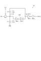
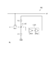
図1は、実施形態1に係わる記憶回路を説明した図である。先ず、実施形態1に係わる記憶回路10を、図1を参照して、説明する。
(Embodiment 1)
"Configuration of memory circuit"
FIG. 1 is a diagram illustrating a memory circuit according to the first embodiment. First, the
図1に示す様に、本実施形態に係わる記憶回路10は、入力信号が入力される入力部INと、第一スイッチSw1と、第一容量素子C1と、第二容量素子C2と、論理部LGCと、第一出力OUT1と、を備えている。第一スイッチSw1はトランジスターで、一端(ソースとドレインとの一方)が入力部INに電気的に接続されており、第一スイッチSw1のゲートGt1には選択信号か非選択信号かが供給される。本実施形態では、第一スイッチSw1はN型トランジスターであり、選択信号は高電位Hであり、非選択信号は低電位Lである。
As shown in FIG. 1, the
第一容量素子C1は、第一容量第一電極C11と第一容量第二電極C12とこれらの電極に挟まれた誘電体膜とを有する。第二容量素子C2は、第二容量第一電極C21と第二容量第二電極C22とこれらの電極に挟まれた誘電体膜とを有する。第一スイッチSw1の他端(ソースとドレインとの他方)と第一容量第一電極C11と第二容量第二電極C22と論理部LGCの入力とが電気的に接続されている。この接続点を第一ノードn1と称する。又、論理部LGCの出力と第二容量第一電極C21とが電気的に接続されている。この接続点を第二ノードn2と称する。第一容量第二電極C12には、負電源電位VSSなどの固定電位が供給される。 The first capacitor element C1 includes a first capacitor first electrode C11, a first capacitor second electrode C12, and a dielectric film sandwiched between these electrodes. The second capacitive element C2 includes a second capacitive first electrode C21, a second capacitive second electrode C22, and a dielectric film sandwiched between these electrodes. The other end (the other of the source and the drain) of the first switch Sw1, the first capacitor first electrode C11, the second capacitor second electrode C22, and the input of the logic unit LGC are electrically connected. This connection point is referred to as a first node n1. Further, the output of the logic part LGC and the second capacitor first electrode C21 are electrically connected. This connection point is referred to as a second node n2. A fixed potential such as a negative power supply potential VSS is supplied to the first capacitor second electrode C12.
記憶回路10への入力信号は、論理1に対応する電位と論理0に対応する電位とである。本実施形態では、論理1に対応する電位を高電位Hとし、これを正電源電位VDDとしている。又、論理0に対応する電位を低電位Lとし、これを負電源電位VSSとしている。尚、厳密には、論理0に対応する電位は負電源電位VSSであるか、或いは負電源電位VSSに近い電位であり、少なくとも負電源電位VSSと正電源電位VDDとの平均電位よりも負電源電位VSS側の値を取る電位であるが、本明細書では、簡便の為に、論理0に対応する電位を低電位Lと記述する。同様に、厳密には、論理1に対応する電位は正電源電位VDDであるか、或いは正電源電位VDDに近い電位であり、少なくとも負電源電位VSSと正電源電位VDDとの平均電位よりも正電源電位VDD側の値を取る電位であるが、本明細書では、簡便の為に、論理1に対応する電位を高電位Hと記述する。
Input signals to the
論理部LGCはバッファー回路を有する事が好ましい。バッファー回路は論理閾値電位Vtripを有し、論理閾値電位Vtripよりも低電位L側の値を取る入力信号をより低電位Lに近づけて出力すると共に、論理閾値電位Vtripよりも高電位H側の値を取る入力信号をより高電位Hに近づけて出力する機能を有する回路である。バッファー回路の一例は、偶数個のインバーター回路を直列に接続する物である。本実施形態では、バッファー回路は、第一インバーターINV1と第二インバーターINV2とが、バッファー回路の入力(第一ノードn1)とバッファー回路の出力(第二ノードn2)との間に、直列に電気的に接続されている。こうすると、インバーターが二個との簡単な構成でバッファー回路を構成する事ができる。 The logic part LGC preferably has a buffer circuit. The buffer circuit has a logical threshold potential Vtrip, and outputs an input signal that takes a value on the low potential L side from the logical threshold potential Vtrip closer to the low potential L, and is on the high potential H side from the logical threshold potential Vtrip. This is a circuit having a function of outputting an input signal that takes a value closer to the high potential H. An example of the buffer circuit is one that connects an even number of inverter circuits in series. In this embodiment, in the buffer circuit, the first inverter INV1 and the second inverter INV2 are electrically connected in series between the input of the buffer circuit (first node n1) and the output of the buffer circuit (second node n2). Connected. In this way, a buffer circuit can be configured with a simple configuration with two inverters.
上述の構成の場合、バッファー回路の論理閾値電位Vtripは第一インバーターINV1の論理閾値電位Vtripとなる。インバーターの論理閾値電位Vtripとは、インバーターが論理1と論理0とを区別する電位である。即ち、インバーターへの入力が論理閾値電位Vtripよりも高ければ、インバーターからの出力を論理閾値電位Vtripよりも低い電位とし、インバーターへの入力が論理閾値電位Vtripよりも低ければ、インバーターからの出力を論理閾値電位Vtripよりも高い電位とする電位がインバーターの論理閾値電位Vtripである。
In the case of the above-described configuration, the logical threshold potential Vtrip of the buffer circuit becomes the logical threshold potential Vtrip of the first inverter INV1. The logic threshold potential Vtrip of the inverter is a potential at which the inverter distinguishes between
論理部LGCをバッファー回路にて構成すると、論理回路に入力された(第一ノードn1の)論理と同じ論理が、短時間の遅延を伴って第二容量第一電極C21(第二ノードn2)に出力される。その結果、第一容量素子C1と第二容量素子C2との容量結合によって第一ノードn1の電位を素早く変化させる事ができる。即ち、記憶回路の第一容量素子C1が記憶する論理に対応する第一ノードn1の電位は、自己の格納論理が変化した場合に、第一容量素子C1と第二容量素子C2との容量結合によってブーストされる。ブースト動作の結果、第一容量第一電極C11の電位は規定電位(正電源電位VDD又は負電源電位VSS)により短期間で近づき、記憶回路へのデータ書き換えを高速に行う事ができる。 When the logic unit LGC is configured by a buffer circuit, the same logic as the logic (of the first node n1) input to the logic circuit has a short delay and the second capacitor first electrode C21 (second node n2). Is output. As a result, the potential of the first node n1 can be quickly changed by capacitive coupling between the first capacitive element C1 and the second capacitive element C2. That is, the potential of the first node n1 corresponding to the logic stored in the first capacitive element C1 of the memory circuit is the capacitive coupling between the first capacitive element C1 and the second capacitive element C2 when the storage logic of the first node n1 changes. Boosted by As a result of the boost operation, the potential of the first capacitor first electrode C11 approaches the specified potential (positive power supply potential VDD or negative power supply potential VSS) in a short period of time, and data rewriting to the memory circuit can be performed at high speed.
更に、記憶回路の誤動作を抑制する事が可能となる。一般にダイナミックランダムアクセスメモリー型の記憶回路では、論理保持は容量素子(本実施形態の第一容量素子C1に相当)への充電量と電荷保持能力に依存する。記憶回路の動作速度が高まるにつれ、容量素子への充電が不十分なままデータラッチ動作が終了してしまう事態が発生する様になる。上記の事態は、図1の回路のように第一スイッチSw1が片方の導電型、つまりN型のトランジスターで構成されているのであれば、高電位H(論理1)を格納する際には常に生じる状態である。例えば3.3V系の電源を用いる記憶回路で高電位を記憶しようとしても、2V程度の電位で論理1を記憶する事になる。その後のデータ維持期間に、電荷漏れによって容量素子の電位が変化すると記憶回路が保持すべき論理が反転する事もあり得る。即ち従来のダイナミックランダムアクセスメモリー型の記憶回路では、記憶回路の動作速度が高まるにつれ誤動作する確率が増大していた。これに対して、本実施形態の記憶回路では、自己の格納論理が変化した場合に、第一容量素子C1と第二容量素子C2との容量結合によって第一ノードn1の電位がブーストされるので、第一容量第一電極C11の電位は規定電位(正電源電位VDD又は負電源電位VSS)により近づき、電荷漏れによって論理反転する誤動作の危険性が低減されている。
Further, malfunction of the memory circuit can be suppressed. In general, in a dynamic random access memory type storage circuit, logical holding depends on the amount of charge and charge holding capacity of a capacitive element (corresponding to the first capacitive element C1 of this embodiment). As the operation speed of the memory circuit increases, a situation occurs in which the data latch operation ends with insufficient charging of the capacitor element. If the first switch Sw1 is composed of one conductivity type, that is, an N-type transistor as in the circuit of FIG. 1, the above situation always occurs when storing a high potential H (logic 1). It is a state that occurs. For example, even if a high potential is stored in a storage circuit using a 3.3V power supply,
尚、バッファー回路の構成は偶数個のインバーターに限られることなく、上述のバッファー部としての機能を果たす物であれば、いかなる形態であっても良い。又、本実施形態では、第二ノードn2の後段に第三インバーターINV3と第四インバーターINV4とから構成される第二のバッファー回路を設け、第二のバッファー回路の出力を記憶回路10からの第二出力OUT2としている。この様に、第二ノードn2の後段に更に幾つかのバッファーを備えていても良い。
The configuration of the buffer circuit is not limited to an even number of inverters, and may take any form as long as it functions as the buffer unit described above. In the present embodiment, the second buffer circuit including the third inverter INV3 and the fourth inverter INV4 is provided at the subsequent stage of the second node n2, and the output of the second buffer circuit is supplied from the
尚、本明細書にて、端子1と端子2とが電気的に接続されているとは、端子1と端子2とが配線により直に接続されている場合の他に、抵抗素子やスイッチング素子を介して接続されている場合を含む。即ち、端子1での電位と端子2での電位とが多少異なっていても、回路上で同じ意味を持たせる場合、端子1と端子2とは電気的に接続されている事になる。従って、例えば、第一出力OUT1の電位を出力させたり遮断させたりする為のスイッチング素子を第二ノードn2と第二出力OUT2との間に設けた場合も、そのスイッチング素子がオン状態では、第二ノードn2の論理が第二出力OUT2に供給されるので、両者は電気的に接続されている事になる。
In this specification, the term “
「原理及び検証」
図2は本実施形態に係わる記憶回路の動作原理を説明した図である。図3は本実施形態に係わる記憶回路の機能を検証した図である。次に、図2乃至3を参照して、本実施形態に係わる記憶回路10の動作原理を説明すると共に、その機能を検証すると共に、その原理を説明する。
"Principle and Verification"
FIG. 2 is a diagram for explaining the operation principle of the memory circuit according to this embodiment. FIG. 3 is a diagram verifying the function of the memory circuit according to this embodiment. Next, the operation principle of the
図2は、入力論理が低電位Lから高電位Hへと変化する第一サンプリングSMP1と、入力論理が高電位Hから高電位Hへと変化する第二サンプリングSMP2と、入力論理が高電位Hから低電位Lへと変化する第三サンプリングSMP3と、入力論理が低電位Lから低電位Lへと変化する第四サンプリングSMP4と、の4通りに変化する場合について動作を説明している。 2 shows a first sampling SMP1 in which the input logic changes from a low potential L to a high potential H, a second sampling SMP2 in which the input logic changes from a high potential H to a high potential H, and an input logic that has a high potential H. The operation is described for the case where the third sampling SMP3 that changes from the low potential L to the low potential L and the fourth sampling SMP4 that changes the input logic from the low potential L to the low potential L change.
第一サンプリングSMP1では、時刻T1に第一スイッチSw1がオンする。この際に、入力論理は低電位Lであり、第一出力OUT1(第二ノードn2)は低電位Lである。時刻T2に入力論理が低電位Lから高電位Hに遷移を開始する。第一ノードn1の電位VCは、論理閾値電位Vtripに達していないので、第一出力OUT1(第二ノードn2)は低電位Lである。時刻T3に第一ノードn1の電位VCが充電され、論理閾値電位Vtripに到達する。第一出力OUT1(第二ノードn2)の論理は反転し、第二ノードn2の電位は高電位Hに遷移する。第一出力OUT1(第二ノードn2)が低電位Lから高電位Hに遷移したので、第一容量素子C1と第二容量素子C2との容量結合によって第一ノードn1の電位VCの電位は高電位H側に更に変化する。大凡の変化量ΔVは、第一ノードn1の全寄生容量をCallとすれば、ΔV=C2/Call×(VDD−VSS)である。このブースティングの効果によって、第一ノードn1の電位は論理閾値電位Vtripをより超えた記憶電位に達する事ができ、記憶回路の動作安定性が高まると共に高速動作が可能となる。又、より短期間内に論理閾値電位Vtripを充分超えた記憶電位に達するので、第一インバーターINV1の貫通電流を抑制でき、消費電流の低減を図る事が可能である。時刻T4に第一スイッチSw1がオフし、サンプリング動作が終了する。第一サンプリングSMP1の期間で第一出力OUT1(第二ノードn2)は低電位Lから高電位Hへと反転する。 In the first sampling SMP1, the first switch Sw1 is turned on at time T1. At this time, the input logic is the low potential L, and the first output OUT1 (second node n2) is the low potential L. The input logic starts transition from the low potential L to the high potential H at time T2. Since the potential VC of the first node n1 does not reach the logical threshold potential Vtrip, the first output OUT1 (second node n2) is at the low potential L. At time T3, the potential VC of the first node n1 is charged and reaches the logical threshold potential Vtrip. The logic of the first output OUT1 (second node n2) is inverted, and the potential of the second node n2 transitions to the high potential H. Since the first output OUT1 (second node n2) transitions from the low potential L to the high potential H, the potential VC of the first node n1 is high due to capacitive coupling between the first capacitive element C1 and the second capacitive element C2. Further changes to the potential H side. The approximate amount of change ΔV is ΔV = C2 / Call × (VDD−VSS) where the total parasitic capacitance of the first node n1 is Call. Due to this boosting effect, the potential of the first node n1 can reach the storage potential that exceeds the logical threshold potential Vtrip, and the operation stability of the storage circuit is improved and high-speed operation is possible. In addition, since the storage potential that sufficiently exceeds the logical threshold potential Vtrip is reached within a shorter period, the through current of the first inverter INV1 can be suppressed, and the current consumption can be reduced. At time T4, the first switch Sw1 is turned off, and the sampling operation ends. The first output OUT1 (second node n2) is inverted from the low potential L to the high potential H during the first sampling SMP1.
第二サンプリングSMP2では、時刻T5に第一スイッチSw1がオンする。入力論理は高電位Hであり、第一出力OUT1(第二ノードn2)は高電位Hである。時刻T6に第一ノードn1の電位VCは充電され、論理閾値電位Vtripを充分超えた電位にある。従って第一出力OUT1(第二ノードn2)の変化はなく、容量結合によるブースティング動作は発生しない。時刻T7に第一スイッチSw1がオフし、サンプリング動作が終了する。第二サンプリングSMP2の期間で第一出力OUT1(第二ノードn2)は高電位Hを維持する。 In the second sampling SMP2, the first switch Sw1 is turned on at time T5. The input logic is high potential H, and the first output OUT1 (second node n2) is high potential H. At time T6, the potential VC of the first node n1 is charged and is at a potential sufficiently exceeding the logical threshold potential Vtrip. Accordingly, there is no change in the first output OUT1 (second node n2), and a boosting operation due to capacitive coupling does not occur. At time T7, the first switch Sw1 is turned off, and the sampling operation ends. The first output OUT1 (second node n2) maintains the high potential H during the period of the second sampling SMP2.
第三サンプリングSMP3では、時刻T8に第一スイッチSw1がオンする。この際に、入力論理は高電位Hであり、第一出力OUT1(第二ノードn2)は高電位Hである。時刻T9に入力論理が高電位Hから低電位Lに遷移を開始する。第一ノードn1の電位VCは論理閾値電位Vtripに達していないので、第一出力OUT1(第二ノードn2)は高電位Hのままである。時刻T10に第一ノードn1の電位VCが放電され、論理閾値電位Vtripに到達する。第一出力OUT1(第二ノードn2)の論理は反転し、第二ノードn2の電位は低電位Lに遷移する。第一出力OUT1(第二ノードn2)が高電位Hから低電位Lに遷移したので、容量結合によって第一ノードn1の電位VCの電位は低電位L側に更に変化する。大凡の変化量ΔVは、第一ノードn1の全寄生容量をCallとすれば、ΔV=C2/Call×(VSS−VDD)である。このブースティングの効果によって、第一ノードn1の電位は論理閾値電位Vtripをより下回った記憶電位に達する事ができ、記憶回路の動作安定性が高まると共に高速動作が可能となる。又、より短期間内に論理閾値電位Vtripを充分下回った記憶電位に達するので、第一インバーターINV1の貫通電流を抑制でき、消費電流の低減を図る事が可能である。時刻T11に第一スイッチSw1がオフし、サンプリング動作が終了する。第三サンプリングSMP3の期間で第一出力OUT1(第二ノードn2)は高電位Hから低電位Lへと反転する。 In the third sampling SMP3, the first switch Sw1 is turned on at time T8. At this time, the input logic is the high potential H, and the first output OUT1 (second node n2) is the high potential H. At time T9, the input logic starts a transition from the high potential H to the low potential L. Since the potential VC of the first node n1 does not reach the logical threshold potential Vtrip, the first output OUT1 (second node n2) remains at the high potential H. At time T10, the potential VC of the first node n1 is discharged and reaches the logical threshold potential Vtrip. The logic of the first output OUT1 (second node n2) is inverted, and the potential of the second node n2 transitions to the low potential L. Since the first output OUT1 (second node n2) transitions from the high potential H to the low potential L, the potential VC of the first node n1 further changes to the low potential L side due to capacitive coupling. The approximate amount of change ΔV is ΔV = C2 / Call × (VSS−VDD) where the total parasitic capacitance of the first node n1 is Call. By this boosting effect, the potential of the first node n1 can reach the storage potential lower than the logical threshold potential Vtrip, so that the operation stability of the storage circuit is improved and high-speed operation is possible. In addition, since the storage potential that is sufficiently lower than the logical threshold potential Vtrip is reached within a shorter period, the through current of the first inverter INV1 can be suppressed, and the current consumption can be reduced. At time T11, the first switch Sw1 is turned off, and the sampling operation ends. In the period of the third sampling SMP3, the first output OUT1 (second node n2) is inverted from the high potential H to the low potential L.
第四サンプリングSMP4では、時刻T12に第一スイッチSw1がオンする。入力論理は低電位Lであり、第一出力OUT1(第二ノードn2)は低電位Lである。時刻T13に第一ノードn1の電位VCは放電され、論理閾値電位Vtripを充分下回った電位にある。従って第一出力OUT1(第二ノードn2)の変化はなく、容量結合によるブースティング動作は発生しない。時刻T14に第一スイッチSw1がオフし、サンプリング動作が終了する。第四サンプリングSMP4の期間で第一出力OUT1(第二ノードn2)は低電位Lを維持する。この様にして、記憶すべき論理の書き換えがなされる。 In the fourth sampling SMP4, the first switch Sw1 is turned on at time T12. The input logic is low potential L, and the first output OUT1 (second node n2) is low potential L. At time T13, the potential VC of the first node n1 is discharged and is at a potential sufficiently lower than the logical threshold potential Vtrip. Accordingly, there is no change in the first output OUT1 (second node n2), and a boosting operation due to capacitive coupling does not occur. At time T14, the first switch Sw1 is turned off, and the sampling operation ends. The first output OUT1 (second node n2) maintains the low potential L during the period of the fourth sampling SMP4. In this way, the logic to be stored is rewritten.
図3は記憶回路10の機能を検証しており、横軸は時間を表し、縦軸は電位を示している。入力信号は10Vの振幅を有する矩形波で、図3では「IN」にて示されている。第一スイッチのゲートGt1に供給される信号は10Vの振幅を有する矩形波で、図3では「Gt1」にて示されている。又、本実施形態に係わる記憶回路10の第一ノードn1での電位VCは、図3では「本実施形態VC」にて示されている。更に、従来技術に相当する比較例の記憶回路の第一ノードn1での電位VCも図3に「比較例VC」にて示されている。比較例の記憶回路とは、一つのトランジスターと一つの容量素子とから構成されるダイナミックランダムアクセスメモリー型の記憶回路である。
FIG. 3 verifies the function of the
図3に示される様に、比較例の記憶回路では、トランジスター(本実施形態の第一スイッチSw1に相当)がN型であるので、高電位Hを記憶する際に、記憶素子のノード(本実施形態の第一ノードn1に相当)の電位(本実施形態のVCに相当)が十分に上がらず、7V程度となっている。これに対して、本実施形態の第一ノードn1での電位VCは素早く10V近傍に到達している事が判る。この様に、本実施形態の記憶回路では高速動作が可能で、記憶された論理を従来の記憶回路よりも長い時間維持する事ができる。 As shown in FIG. 3, in the memory circuit of the comparative example, the transistor (corresponding to the first switch Sw1 of this embodiment) is N-type, and therefore, when storing the high potential H, the node of the memory element (this The potential (corresponding to the first node n1 in the embodiment) (corresponding to VC in the present embodiment) does not rise sufficiently, and is about 7V. On the other hand, it can be seen that the potential VC at the first node n1 of this embodiment quickly reaches around 10V. As described above, the memory circuit of this embodiment can operate at high speed, and the stored logic can be maintained for a longer time than the conventional memory circuit.
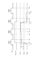
「電気光学装置の回路全体構成」
図4は、実施形態1に係わる電気光学装置の回路の全体構成を説明する図である。以下、図4を参照して電気光学装置の回路構成を説明する。
"Whole circuit configuration of electro-optical device"
FIG. 4 is a diagram for explaining the overall configuration of the circuit of the electro-optical device according to the first embodiment. The circuit configuration of the electro-optical device will be described below with reference to FIG.
上述の記憶回路10は電気光学装置等に使用される。電気光学装置の一例は液晶装置100であり、薄膜トランジスター素子(TFT素子)46を画素45のスイッチング素子として用いたアクティブマトリックス方式の電気光学装置である。図4に示す様に、液晶装置100は表示領域40と信号線駆動回路30と走査線駆動回路20とを少なくとも備えている。
The
表示領域40内には、画素45がm行n列の行列状に設けられている。本実施形態では、一例として800行(m=800)×1280列(n=1280)の行列に画素45が配置されている。画素45は、交差する走査線16と信号線17とによって特定される領域で、一つの画素45は一本の走査線16からその隣の走査線16まで、且つ、一本の信号線17からその隣の信号線17までの領域である。表示領域40の外側の領域には、信号線駆動回路30及び走査線駆動回路20が形成されている。
In the
走査線駆動回路20は画素45を行方向に選択又は非選択する走査信号を各走査線16に出力し、走査線16はこの走査信号を画素45に伝える。走査線駆動回路20はY側シフトレジスター回路21を備えており、Y側シフトレジスター回路21をシフトする信号が、一段毎にシフト出力信号として出力される。このシフト出力信号を用いて走査信号が形成される。尚、各走査線16に供給される走査信号を区別する際には、これらをG1、G2、…、Gmと記述する。
The scanning
信号線駆動回路30は、走査信号に同期して信号線17の各々に画像信号DATを供給する。画像信号DATは論理1又は論理0となるデジタル信号である。この為に、信号線駆動回路30はX側シフトレジスター回路31と一次ラッチ回路32と二次ラッチ回路33とデータ線34とを有している。X側シフトレジスター回路31は、水平走査期間の最初に供給されるスタートパルス信号SPXを、クロック信号CKXの立ち下がり及び立ち上がりで順次シフトして、サンプリング信号を一次ラッチ回路32に順次出力する。一次ラッチ回路32はサンプリング信号に応じて、データ線に供給される画像信号DATを記憶する。一次ラッチ回路32に記憶された画像信号DATは、ラッチ信号LATに応じて、水平走査の帰還期間(ある水平期間が終わり次の水平走査が始まる迄の期間、即ち最初の水平走査を行うスタートパルス信号SPXがX側シフトレジスター回路31の最終出力段を出てから、次の水平走査を行うスタートパルス信号SPXがX側シフトレジスター回路31の第1段の出力段に現れる前)に一斉に二次ラッチ回路33に転送される。二次ラッチ回路33に転送された画像信号DATは、次の水平走査期間が終了する迄、一斉に各信号線17へと供給される。二次ラッチ回路33には画像信号DATと極性信号(図示せず)とに応じて3個の電圧値のうちひとつを出力する電圧セレクターを内包する。尚、各信号線17に供給される画像信号DATを区別する際には、これらをS1、S2、…、Snと記述する。
The signal
記憶回路10は一次ラッチ回路32に利用されている。一次ラッチ回路32では、画像信号DATを記憶する時間が、非常に短い。本実施形態の電気光学装置はデジタル駆動となるので、1フィールドを多数のサブフィールドで構成された表示を行う。サブフィールド数をNsfとし、画像信号DATの相展開数をNsとすれば、一次ラッチ回路32を構成する各記憶回路が画像信号DATを記憶する時間は、1/60/Nsf/800/1280×Nsである。この様な短期間内に画像信号DATを正確に記憶せねばならないので、一次ラッチ回路32には、高速動作に適した本実施形態の記憶回路10が用いられる。具体的な構成としては、第一スイッチSw1のゲートGt1はX側シフトレジスター回路31の出力段に電気的に接続され、ゲートGt1にはX側シフトレジスター回路31をシフトするシフト出力信号が供給される。記憶回路10の入力部INはデータ線34に電気的に接続され、入力部INには画像信号DATが供給される。記憶回路10の第二出力OUT2は、二次ラッチ回路33の入力に電気的に接続され、一次ラッチ回路32に記憶された画像信号DATを二次ラッチ回路33に出力する。
The
「液晶装置の構造」
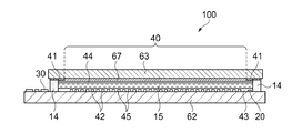
図5は液晶装置の模式断面図である。以下、液晶装置の断面構造を、図5を参照して説明する。尚、以下の形態において、「○○上に」と記載された場合、○○の上に接する様に配置される場合、又は、○○の上に他の構成物を介して配置される場合、又は、○○の上に一部が接する様に配置され一部が他の構成物を介して配置される場合、を表すものとする。
"Structure of liquid crystal device"
FIG. 5 is a schematic cross-sectional view of the liquid crystal device. Hereinafter, a cross-sectional structure of the liquid crystal device will be described with reference to FIG. In addition, in the following forms, when “on XX” is described, when placed on XX, or placed on XX via other components Or, when a part is arranged on OO and a part is arranged through another component, it represents.
液晶装置100では、一対の基板を構成する素子基板62と対向基板63とが、平面視で略矩形枠状に配置されたシール材14にて貼り合わされている。液晶装置100は、シール材14に囲まれた領域内に液晶層15が封入された構成になっている。液晶層15としては、例えば、正の誘電率異方性を有する液晶材料が用いられる。液晶装置100は、シール材14の内周近傍に沿って遮光性材料からなる平面視矩形枠状の遮光膜41が対向基板63に形成されており、この遮光膜41の内側の領域が表示領域40となっている。遮光膜41は、例えば、遮光性材料であるアルミニウム(Al)で形成されており、対向基板63側の表示領域40の外周を区画する様に、更に、上記した様に、表示領域40内で走査線16と信号線17に対向して設けられている。
In the
図5に示す様に、素子基板62の液晶層15側には、複数の画素電極42が形成されており、これら画素電極42を覆う様に第1配向膜43が形成されている。画素電極42は、インジウム錫酸化物(ITO)等の透明導電材料からなる導電膜である。一方、対向基板63の液晶層15側には、格子状の遮光膜41が形成され、その上に平面ベタ状の共通電極67が形成されている。そして、共通電極67上には、第2配向膜44が形成されている。共通電極67は、ITO等の透明導電材料からなる導電膜である。
As shown in FIG. 5, a plurality of
液晶装置100は透過型であって、素子基板62及び対向基板63における光の入射側と出射側とにそれぞれ偏光板(図示せず)等が配置されて用いられる。なお、液晶装置100の構成は、これに限定されず、反射型や半透過型の構成であってもよい。
The
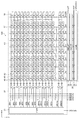
「画素回路」
図6は、液晶装置の表示領域の電気的な構成を示す等価回路図である。以下、液晶装置の電気的な構成を、図6を参照しながら説明する。
"Pixel circuit"
FIG. 6 is an equivalent circuit diagram showing an electrical configuration of the display area of the liquid crystal device. Hereinafter, the electrical configuration of the liquid crystal device will be described with reference to FIG.
図6に示す様に、液晶装置100は、表示領域40を構成する複数の画素45を有している。各画素45には、それぞれ画素電極42が配置されている。又、画素45には、TFT素子46が形成されている。
As shown in FIG. 6, the
TFT素子46は、画素電極42へ通電制御を行うスイッチング素子である。TFT素子46のソース側には、信号線17が電気的に接続されている。各信号線17には、例えば、信号線駆動回路30から画像信号S1、S2、…、Snが供給される様になっている。
The
又、TFT素子46のゲート側には、走査線16が電気的に接続されている。走査線16には、例えば、走査線駆動回路20から所定のタイミングでパルス的に走査信号G1、G2、…、Gmが供給される様になっている。又、TFT素子46のドレイン側には、画素電極42が電気的に接続されている。
Further, the
走査線16から供給された走査信号G1、G2、…、Gmにより、スイッチング素子であるTFT素子46が一定期間だけオン状態となることで、信号線17から供給された画像信号S1、S2、…、Snが、画素電極42を介して画素45に所定のタイミングで書き込まれる様になっている。
.., Gm supplied from the
画素45に書き込まれた所定電位の画像信号S1、S2、…、Snは、画素電極42と共通電極67(図5参照)との間で形成される液晶容量で一定期間保持される。尚、保持された画像信号S1、S2、…、Snの電位が、漏れ電流により、低下する事を抑制すべく、画素電極42と容量線47とで保持容量48が形成されている。
Image signals S1, S2,..., Sn written in the
液晶層15に電圧信号が印加されると、印加された電圧レベルにより、液晶分子の配向状態が変化する。これにより、液晶層15に入射した光が変調されて、画像光が生成される。
When a voltage signal is applied to the
尚、本実施形態では、電気光学装置として液晶装置100を用いて説明したが、この他に電気光学装置としては、電気泳動表示装置や有機EL装置なども対象となる。又、本実施形態では、記憶回路10をTFT素子46と同様に薄膜トランジスターにて構成したが、記憶回路10は半導体基板に形成された半導体集積回路(IC回路)で構成されても良い。記憶回路に適した半導体基板としては、シリコン基板の他にシリコンオンインシュレーター基板などが挙げられる。
In the present embodiment, the
「電子機器」
図7は本実施形態に係わる電子機器を説明する図である。次に、本実施形態の電子機器について、図7を参照して説明する。図7(a)乃至(c)は、上記した液晶装置を備えた電子機器の構成を示す斜視図である。
"Electronics"
FIG. 7 is a diagram for explaining an electronic apparatus according to this embodiment. Next, the electronic apparatus of this embodiment will be described with reference to FIG. 7A to 7C are perspective views illustrating the configuration of an electronic device including the above-described liquid crystal device.
図7(a)に示す様に、液晶装置100を備えたモバイル型のパーソナルコンピューター2000は、液晶装置100と本体部2010とを備える。本体部2010には、電源スイッチ2001及びキーボード2002が設けられている。
As shown in FIG. 7A, the mobile
続いて、図7(b)に示す様に、液晶装置100を備えた携帯電話機3000は、複数の操作ボタン3001及びスクロールボタン3002、並びに表示ユニットとしての液晶装置100を備える。スクロールボタン3002を操作する事によって、液晶装置100に表示される画面がスクロールされる。
Subsequently, as shown in FIG. 7B, the
続いて、図7(c)に示す様に、液晶装置100を備えた情報携帯端末(PDAにPersonal Digital Assistants)4000は、複数の操作ボタン4001及び電源スイッチ4002、並びに表示ユニットとしての液晶装置100を備える。操作ボタン4001を操作すると、住所録やスケジュール帳といった各種の情報が液晶装置100に表示される。
Subsequently, as shown in FIG. 7C, an information portable terminal (Personal Digital Assistants) 4000 including the
尚、液晶装置100が搭載される電子機器としては、図7に示す物の他に、ピコプロジェクター、ヘッドアップディスプレイ、スマートフォン、ヘッドマウントディスプレイ、EVF(Electrical View Finder)、小型プロジェクター、モバイルコンピューター、デジタルカメラ、デジタルビデオカメラ、ディスプレイ、車載機器、オーディオ機器、露光装置や照明機器等、各種電子機器に用いる事ができる。
In addition to the items shown in FIG. 7, the electronic device on which the
以上詳述した様に、本実施形態によれば、以下に示す効果が得られる。まず、第一ノードn1に情報を記憶させる際に、第一容量素子C1と第二容量素子C2との容量結合によって、第一ノードn1の電位を素早く変化させ得るので、高速動作が可能な記憶回路10を実現する事ができる。又、第一ノードn1に書き込まれる電位が論理回路の論理閾値電位Vtripを僅かでも上回るか下回れば良いので、第一スイッチSw1のゲート電圧を高くする必要がない。即ち、低電圧で、従って低消費電力で、高速動作可能な記憶回路10を実現する事ができる。その結果、低消費電力で、高品位表示が可能な電気光学装置を実現する事ができる。更に、高速動作が可能であることから、単位時間あたりの情報量を多く取り扱えることになり、高精細な表示に対応させることが可能となる。又、低消費電力で、高品位表示が可能な電気光学装置を備えた電子機器を実現する事ができる。
As described above in detail, according to the present embodiment, the following effects can be obtained. First, when information is stored in the first node n1, the potential of the first node n1 can be quickly changed by capacitive coupling between the first capacitor element C1 and the second capacitor element C2, so that high speed operation is possible. The
(実施形態2)
図8は、実施形態2に係わる記憶回路の構成を説明した図である。図9は実施形態2に係わる記憶回路の動作原理を説明した図である。次に、図8乃至9を参照して、実施形態2に係わる記憶回路10の構成及び動作原理を説明する。尚、実施形態1と同一の構成部位については、同一の符号を附し、重複する説明は省略する。
(Embodiment 2)
FIG. 8 is a diagram illustrating the configuration of the memory circuit according to the second embodiment. FIG. 9 is a diagram for explaining the operation principle of the memory circuit according to the second embodiment. Next, the configuration and operation principle of the
本実施形態(図8)は実施形態1(図1)と比べて、第二スイッチSw2を備えている点が異なっている。それ以外の構成は、実施形態1とほぼ同様である。本実施形態では、第一ノードn1と第二ノードn2との間に第二スイッチSw2が配置されている。即ち、第二スイッチSw2の一端(ソースとドレインとの一方)は第一ノードn1に電気的に接続され、第二スイッチSw2の他端(ソースとドレインとの他方)は第二ノードn2に電気的に接続されている。第二スイッチSw2のゲートGt2には第二スイッチSw2に対する制御信号が供給される。 The present embodiment (FIG. 8) differs from the first embodiment (FIG. 1) in that a second switch Sw2 is provided. Other configurations are almost the same as those of the first embodiment. In the present embodiment, the second switch Sw2 is disposed between the first node n1 and the second node n2. That is, one end (one of the source and the drain) of the second switch Sw2 is electrically connected to the first node n1, and the other end (the other of the source and the drain) of the second switch Sw2 is electrically connected to the second node n2. Connected. A control signal for the second switch Sw2 is supplied to the gate Gt2 of the second switch Sw2.
第一スイッチSw1と第二スイッチSw2とは、第二スイッチSw2がオフ状態にある期間に第一スイッチSw1はオン状態とされる事が好ましい。第二スイッチSw2がオフ状態の際には論理回路はバッファー回路として機能しているので、斯うする事で、記憶回路10へのデータの書き換えを低消費電力で高速に行う事ができる。
As for 1st switch Sw1 and 2nd switch Sw2, it is preferable that 1st switch Sw1 is made into an ON state in the period when 2nd switch Sw2 is in an OFF state. Since the logic circuit functions as a buffer circuit when the second switch Sw2 is in the OFF state, data rewriting to the
又、第一スイッチSw1と第二スイッチSw2とは、第一スイッチSw1がオフ状態にある期間に第二スイッチSw2はオン状態とされる事が好ましい。即ち、第二スイッチSw2は、記憶回路10のサンプリング動作(記憶すべき論理の書き換え動作)以外の一部の期間にオン状態となっている。第二スイッチSw2がオン状態の際には論理回路は静的記憶装置として機能するので、この構成によれば、記憶された論理を安定的に維持する事ができる。更に、記憶回路10のサンプリング終了時に、サンプリングされた論理は正常であるが第一容量素子C1への書き込み電位が規定よりも不十分であった場合(第一ノードn1に於ける書き込み終了時の電位が正電源電位VDDや負電源電位VSSに極めて近い、とは言えない状態の場合)、第二スイッチSw2に対する制御信号によって自己の格納論理状態(第一ノードn1に於ける電位)を正電源電位VDD又は負電源電位VSSへと再書き込みする動作が行われる。この作用によって、第一ノードn1に記憶された論理に相当する電位は規定電位(正電源電位VDD又は負電源電位VSS)に近づき、電荷漏れによって論理閾値電位Vtripを超える危険性が低減される。即ち、記憶された論理を安定的に保つ事ができる。
The first switch Sw1 and the second switch Sw2 are preferably set so that the second switch Sw2 is on during the period when the first switch Sw1 is off. That is, the second switch Sw2 is in an on state during a part of the period other than the sampling operation (the logic rewrite operation to be stored) of the
図8に示す本実施形態の記憶回路10を電気光学装置の一次ラッチ回路32に使用する場合、第一スイッチSw1のゲートGt1はX側シフトレジスター回路31の出力段に電気的に接続され、ゲートGt1にはX側シフトレジスター回路31をシフトするシフト出力信号が供給される。第二スイッチSw2のゲートGt2はX側シフトレジスター回路31の出力段で、第一スイッチSw1のゲートGt1が接続した出力段のシフト方向に後方の出力段に電気的に接続される。具体的には、シフト出力信号がi段目の出力段から(i+1)段目の出力段へとシフトされており、第一スイッチSw1のゲートGt1がj段目の出力段に電気的に接続されている場合、第二スイッチSw2のゲートGt2は(j+k)段目の出力段に電気的に接続される。kは1以上の整数である。斯うすると、第二スイッチSw2に対する制御信号を別途追加する必要がないので好都合である。記憶回路10の入力部INはデータ線34に電気的に接続され、入力部INには画像信号DATが供給される。記憶回路10の第二出力OUT2は、二次ラッチ回路33の入力に電気的に接続され、一次ラッチ回路32に記憶された画像信号DATを二次ラッチ回路33に出力する。
When the
図9は、入力論理が低電位Lから高電位Hへと変化する第一サンプリングSMP1と、入力論理が高電位Hから高電位Hへと変化する第二サンプリングSMP2と、入力論理が高電位Hから低電位Lへと変化する第三サンプリングSMP3と、入力論理が低電位Lから低電位Lへと変化する第四サンプリングSMP4と、の4通りに変化する場合について動作を説明している。 FIG. 9 shows a first sampling SMP1 in which the input logic changes from a low potential L to a high potential H, a second sampling SMP2 in which the input logic changes from a high potential H to a high potential H, and an input logic that is a high potential H. The operation is described for the case where the third sampling SMP3 that changes from the low potential L to the low potential L and the fourth sampling SMP4 that changes the input logic from the low potential L to the low potential L change.
第一サンプリングSMP1では、時刻T1に第一スイッチSw1がオンする。入力論理は低電位Lであり、第一出力OUT1(第二ノードn2)は低電位Lである。時刻T2に入力論理が低電位Lから高電位Hに遷移を開始する。第一ノードn1の電位VCは論理閾値電位Vtripに達していないので、第一出力OUT1(第二ノードn2)は低電位Lである。時刻T3に第一ノードn1の電位VCが充電され、論理閾値電位Vtripに到達する。第一出力OUT1(第二ノードn2)の論理は反転し、第二ノードn2の電位は高電位Hに遷移する。第一出力OUT1(第二ノードn2)が低電位Lから高電位Hに遷移したので、第一容量素子C1と第二容量素子C2との容量結合によって第一ノードn1の電位VCの電位は高電位H側に更に変化する。大凡の変化量ΔVは第一ノードn1の全寄生容量をCallとすれば、ΔV=C2/Call×(VDD−VSS)である。このブースティングの効果によって、論理閾値電位Vtripをより超えた記憶電位に達する事ができ、記憶回路の動作安定性が高まると共に高速動作が可能となる。又、より短期間内に論理閾値電位Vtripを充分超えた記憶電位に達するので、第一インバーターINV1の貫通電流を抑制でき、消費電流の低減を図る事が可能である。時刻T4に第一スイッチSw1がオフし、サンプリング動作が終了する。第一サンプリングSMP1の期間で第一出力OUT1(第二ノードn2)は低電位Lから高電位Hへと反転する。続いて第二スイッチSw2に対する制御信号によって以下の動作が行われる。時刻T5に第二スイッチSw2がオンする。第一出力OUT1(第二ノードn2)は高電位Hなので、第一ノードn1の電位VCは正電源電位VDDから第二スイッチSw2の閾値電圧Vthを減じた電位値(VDD−Vth)に達する様に再充電が行われる。その結果、第一ノードn1の電位VCはより規定電位(この場合、正電源電位VDD)に近づく事になり記憶回路の動作がより安定する。時刻T6に第二スイッチSw2がオフする。 In the first sampling SMP1, the first switch Sw1 is turned on at time T1. The input logic is low potential L, and the first output OUT1 (second node n2) is low potential L. The input logic starts transition from the low potential L to the high potential H at time T2. Since the potential VC of the first node n1 does not reach the logical threshold potential Vtrip, the first output OUT1 (second node n2) is at the low potential L. At time T3, the potential VC of the first node n1 is charged and reaches the logical threshold potential Vtrip. The logic of the first output OUT1 (second node n2) is inverted, and the potential of the second node n2 transitions to the high potential H. Since the first output OUT1 (second node n2) transitions from the low potential L to the high potential H, the potential VC of the first node n1 is high due to capacitive coupling between the first capacitive element C1 and the second capacitive element C2. Further changes to the potential H side. The approximate amount of change ΔV is ΔV = C2 / Call × (VDD−VSS), assuming that the total parasitic capacitance of the first node n1 is Call. By this boosting effect, the storage potential exceeding the logical threshold potential Vtrip can be reached, and the operation stability of the storage circuit is increased and high-speed operation is possible. In addition, since the storage potential that sufficiently exceeds the logical threshold potential Vtrip is reached within a shorter period, the through current of the first inverter INV1 can be suppressed, and the current consumption can be reduced. At time T4, the first switch Sw1 is turned off, and the sampling operation ends. The first output OUT1 (second node n2) is inverted from the low potential L to the high potential H during the first sampling SMP1. Subsequently, the following operation is performed by a control signal for the second switch Sw2. The second switch Sw2 is turned on at time T5. Since the first output OUT1 (second node n2) is a high potential H, the potential VC of the first node n1 reaches a potential value (VDD−Vth) obtained by subtracting the threshold voltage Vth of the second switch Sw2 from the positive power supply potential VDD. Will be recharged. As a result, the potential VC of the first node n1 becomes closer to the specified potential (in this case, the positive power supply potential VDD), and the operation of the memory circuit becomes more stable. The second switch Sw2 is turned off at time T6.
第二サンプリングSMP2では、時刻T7に第一スイッチSw1がオンする。入力論理は高電位Hであり、第一出力OUT1(第二ノードn2)は高電位Hである。第一ノードn1の電位VCは充電され、論理閾値電位Vtripを充分超えた電位にある。従って、第一出力OUT1(第二ノードn2)に変化はなく、容量結合によるブースティング動作は発生しない。時刻T8に第一スイッチSw1がオフし、サンプリング動作が終了する。第二サンプリングSMP2の期間で第一出力OUT1(第二ノードn2)は高電位Hを維持する。続いて第二スイッチSw2に対する制御信号によって以下の動作が行われる。時刻T9に第二スイッチSw2がオンする。第一出力OUT1(第二ノードn2)は高電位Hなので、第一ノードn1の電位VCは正電源電位VDDから第二スイッチSw2の閾値電圧Vthを減じた電位値(VDD−Vth)に達する様に再充電が行われる。その結果、第一ノードn1の電位VCはより規定電位(この場合、正電源電位VDD)に近づく事になり記憶回路の動作がより安定する。既に第一ノードn1の電位VCがVDD−Vthの電位であれば特に再充電の動作とはならない。時刻T10に第二スイッチSw2がオフする。 In the second sampling SMP2, the first switch Sw1 is turned on at time T7. The input logic is high potential H, and the first output OUT1 (second node n2) is high potential H. The potential VC of the first node n1 is charged and is at a potential sufficiently exceeding the logical threshold potential Vtrip. Accordingly, there is no change in the first output OUT1 (second node n2), and a boosting operation due to capacitive coupling does not occur. At time T8, the first switch Sw1 is turned off, and the sampling operation ends. The first output OUT1 (second node n2) maintains the high potential H during the period of the second sampling SMP2. Subsequently, the following operation is performed by a control signal for the second switch Sw2. The second switch Sw2 is turned on at time T9. Since the first output OUT1 (second node n2) is a high potential H, the potential VC of the first node n1 reaches a potential value (VDD−Vth) obtained by subtracting the threshold voltage Vth of the second switch Sw2 from the positive power supply potential VDD. Will be recharged. As a result, the potential VC of the first node n1 becomes closer to the specified potential (in this case, the positive power supply potential VDD), and the operation of the memory circuit becomes more stable. If the potential VC of the first node n1 is already VDD-Vth, the recharging operation is not particularly performed. The second switch Sw2 is turned off at time T10.
第三サンプリングSMP3では、時刻T11に第一スイッチSw1がオンする。入力論理は高電位Hであり、第一出力OUT1(第二ノードn2)は高電位Hである。時刻T12に入力論理が高電位Hから低電位Lに遷移を開始する。第一ノードn1の電位VCは論理閾値電位Vtripに達していないので、第一出力OUT1(第二ノードn2)は高電位Hのままである。時刻T13に第一ノードn1の電位VCが放電され、論理閾値電位Vtripに到達する。第一出力OUT1(第二ノードn2)の論理は反転し、第二ノードn2の電位は低電位Lに遷移する。第一出力OUT1(第二ノードn2)が高電位Hから低電位Lに遷移したので、容量結合によって第一ノードn1の電位VCの電位は低電位L側に更に変化する。大凡の変化量ΔVは、第一ノードn1の全寄生容量をCallとすれば、ΔV=C2/Call×(VSS−VDD)である。このブースティングの効果によって第一ノードn1の電位VCは論理閾値電位Vtripをより下回った記憶電位に達する事ができ、記憶回路の動作安定性が高まると共に高速動作が可能となる。又、より短期間内に論理閾値電位Vtripを充分下回った記憶電位に達するので、第一インバーターINV1の貫通電流を抑制でき、消費電流の低減を図る事が可能である。時刻T14に第一スイッチSw1がオフし、サンプリング動作が終了する。第三サンプリングSMP3の期間で第一出力OUT1(第二ノードn2)は高電位Hから低電位Lへと反転する。続いて第二スイッチSw2に対する制御信号によって以下の動作が行われる。時刻T15に第二スイッチSw2がオンする。第一出力OUT1(第二ノードn2)は低電位Lなので、第一ノードn1の電位VCは負電源電位VSSに達する様に再放電が行われる。その結果、第一ノードn1の電位VCはより規定電位(この場合、負電源電位VSS)に近づく事になり記憶回路の動作がより安定する。既に第一ノードn1の電位VCが負電源電位VSSの電位であれば特に再放電の動作とはならない。時刻T16に第二スイッチSw2がオフする。 In the third sampling SMP3, the first switch Sw1 is turned on at time T11. The input logic is high potential H, and the first output OUT1 (second node n2) is high potential H. At time T12, the input logic starts transition from the high potential H to the low potential L. Since the potential VC of the first node n1 does not reach the logical threshold potential Vtrip, the first output OUT1 (second node n2) remains at the high potential H. At time T13, the potential VC of the first node n1 is discharged and reaches the logical threshold potential Vtrip. The logic of the first output OUT1 (second node n2) is inverted, and the potential of the second node n2 transitions to the low potential L. Since the first output OUT1 (second node n2) transitions from the high potential H to the low potential L, the potential VC of the first node n1 further changes to the low potential L side due to capacitive coupling. The approximate amount of change ΔV is ΔV = C2 / Call × (VSS−VDD) where the total parasitic capacitance of the first node n1 is Call. By this boosting effect, the potential VC of the first node n1 can reach the storage potential lower than the logical threshold potential Vtrip, so that the operation stability of the storage circuit is improved and high-speed operation is possible. In addition, since the storage potential that is sufficiently lower than the logical threshold potential Vtrip is reached within a shorter period, the through current of the first inverter INV1 can be suppressed, and the current consumption can be reduced. At time T14, the first switch Sw1 is turned off, and the sampling operation ends. In the period of the third sampling SMP3, the first output OUT1 (second node n2) is inverted from the high potential H to the low potential L. Subsequently, the following operation is performed by a control signal for the second switch Sw2. The second switch Sw2 is turned on at time T15. Since the first output OUT1 (second node n2) is at the low potential L, re-discharge is performed so that the potential VC of the first node n1 reaches the negative power supply potential VSS. As a result, the potential VC of the first node n1 is closer to the specified potential (in this case, the negative power supply potential VSS), and the operation of the memory circuit is more stable. If the potential VC of the first node n1 is already the negative power supply potential VSS, the re-discharge operation is not particularly performed. The second switch Sw2 is turned off at time T16.
第四サンプリングSMP4では、時刻T17に第一スイッチSw1がオンする。入力論理は低電位Lであり、第一出力OUT1(第二ノードn2)は低電位Lである。時刻T13に第一ノードn1の電位VCは放電され、論理閾値電位Vtripを充分下回った電位にある。従って、第一出力OUT1(第二ノードn2)に変化はなく、容量結合によるブースティング動作は発生しない。時刻T18に第一スイッチSw1がオフし、サンプリング動作が終了する。第四サンプリングSMP4の期間で第一出力OUT1(第二ノードn2)は低電位Lを維持する。 In the fourth sampling SMP4, the first switch Sw1 is turned on at time T17. The input logic is low potential L, and the first output OUT1 (second node n2) is low potential L. At time T13, the potential VC of the first node n1 is discharged and is at a potential sufficiently lower than the logical threshold potential Vtrip. Accordingly, there is no change in the first output OUT1 (second node n2), and a boosting operation due to capacitive coupling does not occur. At time T18, the first switch Sw1 is turned off, and the sampling operation ends. The first output OUT1 (second node n2) maintains the low potential L during the period of the fourth sampling SMP4.
上述の構成としても、実施形態1と同じ効果が得られる。 Even with the above-described configuration, the same effect as the first embodiment can be obtained.
尚、本発明は上述した実施形態に限定されず、上述した実施形態に種々の変更や改良などを加えることが可能である。変形例を以下に説明する。 The present invention is not limited to the above-described embodiment, and various changes and improvements can be added to the above-described embodiment. A modification will be described below.
(変形例1)
「半導体記憶装置の形態」
図10は、変形例1に係わる半導体記憶回路のメモリーセル構成を説明した図である。次に、本変形例における半導体記憶回路及び電子機器を説明する。尚、実施形態1乃至2と同一の構成部位については、同一の符号を附し、重複する説明は省略する。
(Modification 1)
"Semiconductor memory device configuration"
FIG. 10 is a diagram for explaining a memory cell configuration of a semiconductor memory circuit according to the first modification. Next, a semiconductor memory circuit and an electronic device in this modification will be described. In addition, about the component same as
実施形態1乃至2では記憶回路10は電気光学装置に適応されていた。これに対して、本変形例では、記憶回路10は半導体記憶回路に用いられている点が異なっている。それ以外の構成は、実施形態1とほぼ同様である。半導体記憶装置は、メモリーセルMCが多数配列されたメモリーセルアレイと、メモリーセルアレイ内の一行分のメモリーセルMCを選択するワード線選択回路(行デコーダー)、メモリーセルアレイの一列を選択するビット線選択回路(列デコーダー)、選択されたメモリーセルMCから出力される微小信号(データ)を増幅/複合するセンスアンプ回路等を含んでいる。
In the first and second embodiments, the
図10に示す様に、メモリーセルMCには、実施形態1乃至2にて詳述した記憶回路10が配置されている。具体的には、メモリーセルMCを選択する選択トランジスターとして第一スイッチSw1が設けられ、データを記憶する記憶容量として第一容量素子C1が含まれている。選択トランジスターのゲートはワード線WLに電気的に接続され、ソースとドレインとの一方はビット線BLに電気的に接続され、ソースとドレインとの他方は第一容量第一電極C11(第一ノードn1)に電気的に接続されている。第一容量第二電極C12は負電源電位VSS等の固定電位が供給される電源線に電気的に接続されている。更に、メモリーセルMCには、論理部LGCと第二容量素子C2とが含まれており、これらの接続関係も実施形態1乃至2と同様である。斯うする事で、低消費電力で、高速動作が可能な半導体記憶装置を実現する事ができる。又、上述の半導体記憶装置を電子機器が備えていても良い。これにより、低消費電力で、高速動作が可能な半導体記憶装置を備えた電子機器が実現される。
As shown in FIG. 10, the
BL…ビット線、C1…第一容量素子、C11…第一容量第一電極、C12…第一容量第二電極、C2…第二容量素子、C21…第二容量第一電極、C22…第二容量第二電極、IN…入力部、INV1…第一インバーター、INV2…第二インバーター、INV3…第三インバーター、INV4…第四インバーター、MC…メモリーセル、WL…ワード線、OUT1…第一出力、OUT2…第二出力、Sw1…第一スイッチ、Sw2…第二スイッチ、10…記憶回路、14…シール材、15…液晶層、16…走査線、17…信号線、20…走査線駆動回路、21…Y側シフトレジスター回路、30…信号線駆動回路、31…X側シフトレジスター回路、32…一次ラッチ回路、33…二次ラッチ回路、34…データ線、40…表示領域、41…遮光膜、42…画素電極、43…第1配向膜、44…第2配向膜、45…画素、46…TFT素子、47…容量線、48…保持容量、62…素子基板、63…対向基板、67…共通電極、100…液晶装置、2000…モバイル型のパーソナルコンピューター、2001…電源スイッチ、2002…キーボード、2010…本体部、3000…携帯電話機、3001…操作ボタン、3002…スクロールボタン、4000…情報携帯端末、4001…複数の操作ボタン、4002…電源スイッチ。
BL ... bit line, C1 ... first capacitor element, C11 ... first capacitor first electrode, C12 ... first capacitor second electrode, C2 ... second capacitor element, C21 ... second capacitor first electrode, C22 ... second Capacitance second electrode, IN ... input, INV1 ... first inverter, INV2 ... second inverter, INV3 ... third inverter, INV4 ... fourth inverter, MC ... memory cell, WL ... word line, OUT1 ... first output, OUT2 ... second output, Sw1 ... first switch, Sw2 ... second switch, 10 ... memory circuit, 14 ... sealing material, 15 ... liquid crystal layer, 16 ... scan line, 17 ... signal line, 20 ... scan line drive circuit, DESCRIPTION OF
Claims (9)
前記第一スイッチの他端と前記第一容量第一電極と前記第二容量第二電極と前記論理部の入力とが電気的に接続され(第一ノードと称する)、
前記論理部の出力と前記第二容量第一電極とが電気的に接続される(第二ノードと称する)事を特徴とする記憶回路。 A first switch having one end electrically connected to the input portion, a first capacitor first electrode and a first capacitor second electrode, a second capacitor first electrode and a second capacitor second A second capacitive element having an electrode, and a logic unit,
The other end of the first switch, the first capacitor first electrode, the second capacitor second electrode, and the input of the logic unit are electrically connected (referred to as a first node),
An output of the logic unit and the second capacitor first electrode are electrically connected (referred to as a second node).
前記第二スイッチの一端は前記第一ノードに電気的に接続され、
前記第二スイッチの他端は前記第二ノードに電気的に接続される事を特徴とする請求項1又は2に記載の記憶回路。 With a second switch,
One end of the second switch is electrically connected to the first node;
The memory circuit according to claim 1, wherein the other end of the second switch is electrically connected to the second node.
Priority Applications (1)
| Application Number | Priority Date | Filing Date | Title |
|---|---|---|---|
| JP2013223981A JP6135459B2 (en) | 2013-10-29 | 2013-10-29 | Memory circuit, electro-optical device, semiconductor memory device, and electronic apparatus |
Applications Claiming Priority (1)
| Application Number | Priority Date | Filing Date | Title |
|---|---|---|---|
| JP2013223981A JP6135459B2 (en) | 2013-10-29 | 2013-10-29 | Memory circuit, electro-optical device, semiconductor memory device, and electronic apparatus |
Publications (3)
| Publication Number | Publication Date |
|---|---|
| JP2015088198A true JP2015088198A (en) | 2015-05-07 |
| JP2015088198A5 JP2015088198A5 (en) | 2016-08-25 |
| JP6135459B2 JP6135459B2 (en) | 2017-05-31 |
Family
ID=53050820
Family Applications (1)
| Application Number | Title | Priority Date | Filing Date |
|---|---|---|---|
| JP2013223981A Expired - Fee Related JP6135459B2 (en) | 2013-10-29 | 2013-10-29 | Memory circuit, electro-optical device, semiconductor memory device, and electronic apparatus |
Country Status (1)
| Country | Link |
|---|---|
| JP (1) | JP6135459B2 (en) |
Citations (4)
| Publication number | Priority date | Publication date | Assignee | Title |
|---|---|---|---|---|
| JPS6010912A (en) * | 1983-06-30 | 1985-01-21 | Mitsubishi Electric Corp | Semiconductor integrated circuit |
| WO2009063542A1 (en) * | 2007-11-12 | 2009-05-22 | Fujitsu Microelectronics Limited | Semiconductor device |
| JP2010511185A (en) * | 2006-11-28 | 2010-04-08 | コーニンクレッカ フィリップス エレクトロニクス エヌ ヴィ | Active matrix array device |
| JP2013085238A (en) * | 2011-09-30 | 2013-05-09 | Semiconductor Energy Lab Co Ltd | Storage element and signal processing circuit |
-
2013
- 2013-10-29 JP JP2013223981A patent/JP6135459B2/en not_active Expired - Fee Related
Patent Citations (4)
| Publication number | Priority date | Publication date | Assignee | Title |
|---|---|---|---|---|
| JPS6010912A (en) * | 1983-06-30 | 1985-01-21 | Mitsubishi Electric Corp | Semiconductor integrated circuit |
| JP2010511185A (en) * | 2006-11-28 | 2010-04-08 | コーニンクレッカ フィリップス エレクトロニクス エヌ ヴィ | Active matrix array device |
| WO2009063542A1 (en) * | 2007-11-12 | 2009-05-22 | Fujitsu Microelectronics Limited | Semiconductor device |
| JP2013085238A (en) * | 2011-09-30 | 2013-05-09 | Semiconductor Energy Lab Co Ltd | Storage element and signal processing circuit |
Also Published As
| Publication number | Publication date |
|---|---|
| JP6135459B2 (en) | 2017-05-31 |
Similar Documents
| Publication | Publication Date | Title |
|---|---|---|
| CN108281123B (en) | Shift register unit, gate drive circuit, display device and drive method | |
| KR101933332B1 (en) | Goa circuit based on oxide semiconductor thin film transistor | |
| US7193593B2 (en) | Liquid crystal display device and method of driving a liquid crystal display device | |
| JP4415393B2 (en) | Driving circuit, liquid crystal device, electronic apparatus, and driving method of liquid crystal device | |
| US10325553B2 (en) | Pixel circuit and method for driving a light emitting device and organic light emitting display panel | |
| KR101861350B1 (en) | Gate driver and display device including the same | |
| US11645969B2 (en) | Display device, gate drive circuit, shift register and control method thereof | |
| US20150325200A1 (en) | Source driver and display device including the same | |
| US20040041764A1 (en) | Liquid crystal display device and method of driving a liquid crystal display device | |
| US11217148B2 (en) | Shift register unit, driving method, gate driver on array and display device | |
| US20150187298A1 (en) | Display device and method of driving the same | |
| US11217175B2 (en) | Pixel-driving circuit and method, and a display utilizing the same | |
| CN109166542B (en) | Shifting register unit, driving method, grid driving circuit and display device | |
| US8836633B2 (en) | Display driving circuit and display panel using the same | |
| US20170103722A1 (en) | Shift register unit, gate driving circuit and display apparatus | |
| KR20140131137A (en) | Shift register and flat panel display device using the same | |
| KR20180057975A (en) | Shift resister, image display device containing the same and method of driving the same | |
| WO2012023467A1 (en) | Display device | |
| JP6870596B2 (en) | Liquid crystal display device and its driving method | |
| US8144098B2 (en) | Dot-matrix display refresh charging/discharging control method and system | |
| KR102015848B1 (en) | Liquid crystal display device | |
| US8390611B2 (en) | Image display system and gate driver circuit | |
| US10679580B2 (en) | Pixel circuit, driving method thereof and display panel | |
| CN113889020B (en) | GOA circuit and display panel | |
| JP6135459B2 (en) | Memory circuit, electro-optical device, semiconductor memory device, and electronic apparatus |
Legal Events
| Date | Code | Title | Description |
|---|---|---|---|
| RD04 | Notification of resignation of power of attorney |
Free format text: JAPANESE INTERMEDIATE CODE: A7424 Effective date: 20160617 |
|
| RD03 | Notification of appointment of power of attorney |
Free format text: JAPANESE INTERMEDIATE CODE: A7423 Effective date: 20160624 |
|
| A521 | Request for written amendment filed |
Free format text: JAPANESE INTERMEDIATE CODE: A523 Effective date: 20160711 |
|
| A621 | Written request for application examination |
Free format text: JAPANESE INTERMEDIATE CODE: A621 Effective date: 20160711 |
|
| A977 | Report on retrieval |
Free format text: JAPANESE INTERMEDIATE CODE: A971007 Effective date: 20161227 |
|
| A131 | Notification of reasons for refusal |
Free format text: JAPANESE INTERMEDIATE CODE: A131 Effective date: 20170110 |
|
| A521 | Request for written amendment filed |
Free format text: JAPANESE INTERMEDIATE CODE: A523 Effective date: 20170209 |
|
| TRDD | Decision of grant or rejection written | ||
| A01 | Written decision to grant a patent or to grant a registration (utility model) |
Free format text: JAPANESE INTERMEDIATE CODE: A01 Effective date: 20170328 |
|
| A61 | First payment of annual fees (during grant procedure) |
Free format text: JAPANESE INTERMEDIATE CODE: A61 Effective date: 20170410 |
|
| R150 | Certificate of patent or registration of utility model |
Ref document number: 6135459 Country of ref document: JP Free format text: JAPANESE INTERMEDIATE CODE: R150 |
|
| LAPS | Cancellation because of no payment of annual fees |