JP2015050465A - Power semiconductor device and method of manufacturing power semiconductor device - Google Patents
Power semiconductor device and method of manufacturing power semiconductor device Download PDFInfo
- Publication number
- JP2015050465A JP2015050465A JP2014176971A JP2014176971A JP2015050465A JP 2015050465 A JP2015050465 A JP 2015050465A JP 2014176971 A JP2014176971 A JP 2014176971A JP 2014176971 A JP2014176971 A JP 2014176971A JP 2015050465 A JP2015050465 A JP 2015050465A
- Authority
- JP
- Japan
- Prior art keywords
- cooling
- housing member
- power semiconductor
- cooling housing
- semiconductor device
- Prior art date
- Legal status (The legal status is an assumption and is not a legal conclusion. Google has not performed a legal analysis and makes no representation as to the accuracy of the status listed.)
- Withdrawn
Links
Images


Classifications
-
- H—ELECTRICITY
- H01—ELECTRIC ELEMENTS
- H01L—SEMICONDUCTOR DEVICES NOT COVERED BY CLASS H10
- H01L23/00—Details of semiconductor or other solid state devices
- H01L23/34—Arrangements for cooling, heating, ventilating or temperature compensation ; Temperature sensing arrangements
- H01L23/36—Selection of materials, or shaping, to facilitate cooling or heating, e.g. heatsinks
- H01L23/367—Cooling facilitated by shape of device
- H01L23/3675—Cooling facilitated by shape of device characterised by the shape of the housing
-
- H—ELECTRICITY
- H05—ELECTRIC TECHNIQUES NOT OTHERWISE PROVIDED FOR
- H05K—PRINTED CIRCUITS; CASINGS OR CONSTRUCTIONAL DETAILS OF ELECTRIC APPARATUS; MANUFACTURE OF ASSEMBLAGES OF ELECTRICAL COMPONENTS
- H05K7/00—Constructional details common to different types of electric apparatus
- H05K7/20—Modifications to facilitate cooling, ventilating, or heating
- H05K7/2089—Modifications to facilitate cooling, ventilating, or heating for power electronics, e.g. for inverters for controlling motor
- H05K7/20927—Liquid coolant without phase change
-
- H—ELECTRICITY
- H01—ELECTRIC ELEMENTS
- H01L—SEMICONDUCTOR DEVICES NOT COVERED BY CLASS H10
- H01L21/00—Processes or apparatus adapted for the manufacture or treatment of semiconductor or solid state devices or of parts thereof
- H01L21/02—Manufacture or treatment of semiconductor devices or of parts thereof
- H01L21/04—Manufacture or treatment of semiconductor devices or of parts thereof the devices having at least one potential-jump barrier or surface barrier, e.g. PN junction, depletion layer or carrier concentration layer
- H01L21/48—Manufacture or treatment of parts, e.g. containers, prior to assembly of the devices, using processes not provided for in a single one of the subgroups H01L21/06 - H01L21/326
- H01L21/4814—Conductive parts
- H01L21/4871—Bases, plates or heatsinks
- H01L21/4882—Assembly of heatsink parts
-
- H—ELECTRICITY
- H01—ELECTRIC ELEMENTS
- H01L—SEMICONDUCTOR DEVICES NOT COVERED BY CLASS H10
- H01L23/00—Details of semiconductor or other solid state devices
- H01L23/34—Arrangements for cooling, heating, ventilating or temperature compensation ; Temperature sensing arrangements
- H01L23/36—Selection of materials, or shaping, to facilitate cooling or heating, e.g. heatsinks
- H01L23/367—Cooling facilitated by shape of device
- H01L23/3672—Foil-like cooling fins or heat sinks
-
- H—ELECTRICITY
- H01—ELECTRIC ELEMENTS
- H01L—SEMICONDUCTOR DEVICES NOT COVERED BY CLASS H10
- H01L23/00—Details of semiconductor or other solid state devices
- H01L23/34—Arrangements for cooling, heating, ventilating or temperature compensation ; Temperature sensing arrangements
- H01L23/36—Selection of materials, or shaping, to facilitate cooling or heating, e.g. heatsinks
- H01L23/367—Cooling facilitated by shape of device
- H01L23/3677—Wire-like or pin-like cooling fins or heat sinks
-
- H—ELECTRICITY
- H01—ELECTRIC ELEMENTS
- H01L—SEMICONDUCTOR DEVICES NOT COVERED BY CLASS H10
- H01L24/00—Arrangements for connecting or disconnecting semiconductor or solid-state bodies; Methods or apparatus related thereto
- H01L24/80—Methods for connecting semiconductor or other solid state bodies using means for bonding being attached to, or being formed on, the surface to be connected
- H01L24/83—Methods for connecting semiconductor or other solid state bodies using means for bonding being attached to, or being formed on, the surface to be connected using a layer connector
-
- H—ELECTRICITY
- H01—ELECTRIC ELEMENTS
- H01L—SEMICONDUCTOR DEVICES NOT COVERED BY CLASS H10
- H01L2224/00—Indexing scheme for arrangements for connecting or disconnecting semiconductor or solid-state bodies and methods related thereto as covered by H01L24/00
- H01L2224/80—Methods for connecting semiconductor or other solid state bodies using means for bonding being attached to, or being formed on, the surface to be connected
- H01L2224/83—Methods for connecting semiconductor or other solid state bodies using means for bonding being attached to, or being formed on, the surface to be connected using a layer connector
- H01L2224/832—Applying energy for connecting
- H01L2224/83237—Applying energy for connecting using an electron beam
-
- H—ELECTRICITY
- H01—ELECTRIC ELEMENTS
- H01L—SEMICONDUCTOR DEVICES NOT COVERED BY CLASS H10
- H01L2224/00—Indexing scheme for arrangements for connecting or disconnecting semiconductor or solid-state bodies and methods related thereto as covered by H01L24/00
- H01L2224/80—Methods for connecting semiconductor or other solid state bodies using means for bonding being attached to, or being formed on, the surface to be connected
- H01L2224/83—Methods for connecting semiconductor or other solid state bodies using means for bonding being attached to, or being formed on, the surface to be connected using a layer connector
- H01L2224/832—Applying energy for connecting
- H01L2224/83238—Applying energy for connecting using electric resistance welding, i.e. ohmic heating
-
- H—ELECTRICITY
- H01—ELECTRIC ELEMENTS
- H01L—SEMICONDUCTOR DEVICES NOT COVERED BY CLASS H10
- H01L2224/00—Indexing scheme for arrangements for connecting or disconnecting semiconductor or solid-state bodies and methods related thereto as covered by H01L24/00
- H01L2224/80—Methods for connecting semiconductor or other solid state bodies using means for bonding being attached to, or being formed on, the surface to be connected
- H01L2224/83—Methods for connecting semiconductor or other solid state bodies using means for bonding being attached to, or being formed on, the surface to be connected using a layer connector
- H01L2224/838—Bonding techniques
- H01L2224/83801—Soldering or alloying
-
- H—ELECTRICITY
- H01—ELECTRIC ELEMENTS
- H01L—SEMICONDUCTOR DEVICES NOT COVERED BY CLASS H10
- H01L2924/00—Indexing scheme for arrangements or methods for connecting or disconnecting semiconductor or solid-state bodies as covered by H01L24/00
- H01L2924/10—Details of semiconductor or other solid state devices to be connected
- H01L2924/11—Device type
- H01L2924/12—Passive devices, e.g. 2 terminal devices
- H01L2924/1204—Optical Diode
- H01L2924/12042—LASER
-
- H—ELECTRICITY
- H01—ELECTRIC ELEMENTS
- H01L—SEMICONDUCTOR DEVICES NOT COVERED BY CLASS H10
- H01L2924/00—Indexing scheme for arrangements or methods for connecting or disconnecting semiconductor or solid-state bodies as covered by H01L24/00
- H01L2924/10—Details of semiconductor or other solid state devices to be connected
- H01L2924/11—Device type
- H01L2924/13—Discrete devices, e.g. 3 terminal devices
- H01L2924/1304—Transistor
- H01L2924/1305—Bipolar Junction Transistor [BJT]
- H01L2924/13055—Insulated gate bipolar transistor [IGBT]
-
- H—ELECTRICITY
- H01—ELECTRIC ELEMENTS
- H01L—SEMICONDUCTOR DEVICES NOT COVERED BY CLASS H10
- H01L2924/00—Indexing scheme for arrangements or methods for connecting or disconnecting semiconductor or solid-state bodies as covered by H01L24/00
- H01L2924/10—Details of semiconductor or other solid state devices to be connected
- H01L2924/11—Device type
- H01L2924/13—Discrete devices, e.g. 3 terminal devices
- H01L2924/1304—Transistor
- H01L2924/1306—Field-effect transistor [FET]
- H01L2924/13091—Metal-Oxide-Semiconductor Field-Effect Transistor [MOSFET]
-
- H—ELECTRICITY
- H01—ELECTRIC ELEMENTS
- H01L—SEMICONDUCTOR DEVICES NOT COVERED BY CLASS H10
- H01L2924/00—Indexing scheme for arrangements or methods for connecting or disconnecting semiconductor or solid-state bodies as covered by H01L24/00
- H01L2924/15—Details of package parts other than the semiconductor or other solid state devices to be connected
- H01L2924/151—Die mounting substrate
- H01L2924/156—Material
- H01L2924/157—Material with a principal constituent of the material being a metal or a metalloid, e.g. boron [B], silicon [Si], germanium [Ge], arsenic [As], antimony [Sb], tellurium [Te] and polonium [Po], and alloys thereof
- H01L2924/15738—Material with a principal constituent of the material being a metal or a metalloid, e.g. boron [B], silicon [Si], germanium [Ge], arsenic [As], antimony [Sb], tellurium [Te] and polonium [Po], and alloys thereof the principal constituent melting at a temperature of greater than or equal to 950 C and less than 1550 C
- H01L2924/15747—Copper [Cu] as principal constituent
-
- H—ELECTRICITY
- H01—ELECTRIC ELEMENTS
- H01L—SEMICONDUCTOR DEVICES NOT COVERED BY CLASS H10
- H01L2924/00—Indexing scheme for arrangements or methods for connecting or disconnecting semiconductor or solid-state bodies as covered by H01L24/00
- H01L2924/20—Parameters
- H01L2924/201—Temperature ranges
- H01L2924/20103—Temperature range 60 C=<T<100 C, 333.15 K =< T< 373.15K
-
- H—ELECTRICITY
- H01—ELECTRIC ELEMENTS
- H01L—SEMICONDUCTOR DEVICES NOT COVERED BY CLASS H10
- H01L2924/00—Indexing scheme for arrangements or methods for connecting or disconnecting semiconductor or solid-state bodies as covered by H01L24/00
- H01L2924/20—Parameters
- H01L2924/201—Temperature ranges
- H01L2924/20104—Temperature range 100 C=<T<150 C, 373.15 K =< T < 423.15K
Abstract
Description
本発明は、パワー半導体装置に関するものである。加えて本発明は、パワー半導体装置を製造するための方法に関するものである。 The present invention relates to a power semiconductor device. In addition, the present invention relates to a method for manufacturing a power semiconductor device.
従来技術から公知のパワー半導体装置では、一般的に、例えばパワー半導体スイッチやダイオードのような複数のパワー半導体構成要素が、一枚の基板上に配設されており、また、基板の導電層、並びに、ボンディングワイヤ及び/又はフィルム複合材料(フィルムコンポジット)を用いて、互いに導電的に接続されている。パワー半導体スイッチはその際、一般に、例えばIGBT(絶縁ゲート型バイポーラトランジスタ:Insulated Gate Bipolar Transistor)又はMOSFETs(金属酸化物半導体電界効果トランジスタ:Metal Oxide Semiconductor Field Effect Transistor)のようなトランジスタの形態で、存在する。 In power semiconductor devices known from the prior art, in general, a plurality of power semiconductor components such as, for example, power semiconductor switches and diodes are arranged on a single substrate, and the conductive layer of the substrate, In addition, they are electrically connected to each other using a bonding wire and / or a film composite material (film composite). In this case, power semiconductor switches generally exist in the form of transistors such as IGBTs (Insulated Gate Bipolar Transistors) or MOSFETs (Metal Oxide Semiconductor Field Effect Transistors). To do.
基板上に配設されたパワー半導体構成要素は、その際しばしば、単独の又は複数の所謂ハーフブリッジ回路に、導電的に接続されており、それらは、例えば電圧及び電流を順変換及び逆変換するために利用される。 The power semiconductor components arranged on the substrate are often conductively connected to one or more so-called half-bridge circuits, which forward and reverse convert voltages and currents, for example. Used for.
パワー半導体装置の駆動時には、パワー半導体構成要素には、電気的な損失が発生し、これはパワー半導体構成要素の発熱を導く。パワー半導体装置構成要素を冷却するために、この分野において一般的なパワー半導体装置はしばしば、冷却液によって貫流される冷却体を有しており、これは熱伝導的にパワー半導体構成要素と連結されている。 When the power semiconductor device is driven, an electrical loss occurs in the power semiconductor component, which leads to heat generation of the power semiconductor component. In order to cool power semiconductor device components, power semiconductor devices common in this field often have a cooling body that is flowed by a coolant, which is thermally coupled to the power semiconductor components. ing.
特許文献1からは、除去部を有し、液体によって貫流される冷却体を備えること、及び、パワー半導体構成要素を有するパワー半導体モジュールの冷却プレートを除去部内に配設すること、が知られている。これにより、パワー半導体構成要素の冷却液に対する良好な熱排出が達成される。この場合、パワー半導体装置の通常長期間で想定される耐用年数に渡って、冷却液の漏れを確実に避けるために、冷却プレートが長期に渡り確実に冷却体に対して密閉されていなければならないことが不利である。 From Patent Document 1, it is known to have a cooling body that has a removal portion and is flown by a liquid, and to arrange a cooling plate of a power semiconductor module having a power semiconductor component in the removal portion. Yes. This achieves good heat dissipation from the power semiconductor component coolant. In this case, the cooling plate must be securely sealed to the cooling body for a long period of time in order to reliably avoid leakage of the cooling liquid over the expected life of the power semiconductor device. It is disadvantageous.
本発明の課題は、パワー半導体構成要素から、液体によって貫流されるパワー半導体装置の冷却体への、良好な熱伝導を有するパワー半導体装置にして、また、冷却体が長期間に渡って、確実に密閉されているようなパワー半導体装置を達成することである。 An object of the present invention is to provide a power semiconductor device having good heat conduction from the power semiconductor component to the cooling body of the power semiconductor device that is flowed by the liquid, and the cooling body is reliable over a long period of time. It is to achieve a power semiconductor device that is hermetically sealed.
この課題は、パワー半導体モジュール及び液体により貫流可能な冷却体を有する、以下の様なパワー半導体装置により解決される、つまり、パワー半導体モジュールが、導電性の導電路上に配設されているパワー半導体構成要素を有しており、パワー半導体モジュールが、非導電性の絶縁層及び冷却プレートを有しており、絶縁層が導電路と冷却プレートの間に配設されており、冷却体が第一の冷却ハウジング部材及び第二の冷却ハウジング部材を有し、その第一の冷却ハウジング部材が当該第一の冷却ハウジングを貫通する除去部(カットアウト部)を有しており、冷却プレートが除去部内に配設されており、第一及び第二の冷却ハウジング部材が、パワー半導体構成要素から背けられた冷却体の面(パワー半導体構成要素とは反対側の冷却体の面)に、空所が形成されるような形態を有しており、また、そのように互いに配設されており、冷却プレートが、冷却プレートの周りを取り囲む第一の溶接シームを用いて、第一の冷却ハウジング部材と接続されており、第一の溶接シームが冷却プレートを第一の冷却ハウジング部材に対して密閉しており、第二の冷却ハウジング部材が第一の冷却ハウジング部材と接続されているような、パワー半導体装置により解決される。 This problem is solved by the following power semiconductor device having a power semiconductor module and a cooling body that can flow through with a liquid, that is, a power semiconductor in which the power semiconductor module is disposed on a conductive path. The power semiconductor module has a non-conductive insulating layer and a cooling plate, the insulating layer is disposed between the conductive path and the cooling plate, and the cooling body is first The cooling housing member and the second cooling housing member, the first cooling housing member has a removal portion (cutout portion) penetrating the first cooling housing, and the cooling plate is in the removal portion. The first and second cooling housing members are disposed on the surface of the cooling body facing away from the power semiconductor component (cooling on the side opposite to the power semiconductor component). Using a first welded seam that has a configuration such that voids are formed in the body surface) and are so arranged that the cooling plate surrounds the cooling plate. Connected to the first cooling housing member, the first welding seam seals the cooling plate against the first cooling housing member, and the second cooling housing member is the first cooling housing member. It is solved by a power semiconductor device such as
更に、この課題は、以下の方法工程を有する、パワー半導体装置を製造するための方法によって解決される:
a)電気導電性の導電路上に配設されているパワー半導体構成要素を有するパワー半導体モジュールの準備、及び、第一の冷却ハウジング部材の準備、及び、第二の冷却ハウジング部材の準備、が行われる工程、その際、パワー半導体モジュールは、非電気導電性の絶縁層及び冷却プレートを有しており、絶縁層は導電路及び冷却プレートの間に配設されており、また、第一の冷却ハウジング部材は、第一の冷却ハウジング部材を貫通する除去部を有している。
b)第一の冷却ハウジング部材の除去部への冷却プレートの配設が行われる工程。
c)冷却プレートの第一の冷却ハウジング部材との溶接が、冷却プレートの周りを取り囲み、冷却プレートを第一の冷却ハウジング部材に対して密閉する、第一の溶接シームが発生するように行われる工程にして、冷却プレートの第一の冷却ハウジング部材との当該溶接は、パワー半導体構成要素から背けられている冷却プレートの面にて行われる工程。
d)第一の冷却ハウジング部材に対する第二の冷却ハウジング部材の配設が行われる工程にして、第一の冷却ハウジング部材に対する第二の冷却ハウジング部材の当該配設が、冷却プレートのパワー半導体構成要素から背けられた面に空所を形成するように、また、第一及び第二の冷却ハウジング部材がそのような形状を有するように行われる工程。
e)第二の冷却ハウジング部材の第一の冷却ハウジング部材との接続が行われる工程。
Furthermore, this problem is solved by a method for manufacturing a power semiconductor device having the following method steps:
a) Preparation of a power semiconductor module having a power semiconductor component disposed on an electrically conductive path, preparation of a first cooling housing member, and preparation of a second cooling housing member The power semiconductor module has a non-electrically conductive insulating layer and a cooling plate, the insulating layer being disposed between the conductive path and the cooling plate, and the first cooling The housing member has a removal portion that penetrates the first cooling housing member.
b) A step in which the cooling plate is disposed on the removal portion of the first cooling housing member.
c) Welding of the cooling plate with the first cooling housing member occurs such that a first welding seam is generated that surrounds the cooling plate and seals the cooling plate to the first cooling housing member. In the process, the welding of the cooling plate to the first cooling housing member is performed on the surface of the cooling plate facing away from the power semiconductor component.
d) In the step of arranging the second cooling housing member with respect to the first cooling housing member, the arrangement of the second cooling housing member with respect to the first cooling housing member is the power semiconductor configuration of the cooling plate. A step performed to form a cavity in a surface away from the element and so that the first and second cooling housing members have such a shape.
e) A step of connecting the second cooling housing member with the first cooling housing member.
本方法の有利な構成は、パワー半導体装置の有利な構成と類似しており、そして、逆もまた同様である。 The advantageous configuration of the method is similar to the advantageous configuration of the power semiconductor device and vice versa.
本発明の有利な構成は、従属請求項からもたらされる。 Advantageous configurations of the invention result from the dependent claims.
第一の溶接シームが、冷却プレートの水平方向の側面(水平方向に存する側面)を、除去部を画定する第一の冷却ハウジング部材の水平方向の側面と接続する場合に、有利であることが明らかになった。これにより、冷却体の確実な密閉が保障される。 It may be advantageous if the first weld seam connects the horizontal side of the cooling plate (the side that lies in the horizontal direction) with the horizontal side of the first cooling housing member that defines the removal. It was revealed. This ensures a reliable sealing of the cooling body.
更に、第一の溶接シームが空所側に配設されている場合に、有利であることが明らかになった。本発明の意味では、空所側に配設された溶接シームとしては、空所の面から構成された溶接シームが理解されることが指摘される。これは以下の様な大きな利点を有している、つまり、第一の溶接シームの溶接の際に必要な大きな入熱が、冷却プレートのパワー半導体構成要素から背けられた面で行われ、従ってそれはパワー半導体構成要素の面では行われず、それにより第一の溶接シームの溶接の際に、精密なパワー半導体構成要素の損傷が確実に避けられる、という利点を有している。加えて、冷却プレートは、パワー半導体スイッチ及び導電路を、場合によっては溶接時に分離する液体材料から保護する。冷却プレートは、空間的に確実に溶接プロセスを、パワー半導体構成要素及び導電路から分離する。 Furthermore, it has proved advantageous when the first weld seam is arranged on the cavity side. In the sense of the present invention, it is pointed out that a weld seam arranged on the side of a void is understood as a weld seam constructed from the surface of the void. This has the following great advantages: the large heat input required for welding the first weld seam takes place on the side of the cooling plate facing away from the power semiconductor component, and thus It does not take place in terms of the power semiconductor component, which has the advantage that it ensures that damage to the precision power semiconductor component is avoided during the welding of the first weld seam. In addition, the cooling plate protects the power semiconductor switch and the conductive path from a liquid material that possibly separates during welding. The cooling plate spatially and reliably separates the welding process from the power semiconductor components and the conductive paths.
更に、第一の溶接シームが、パワー半導体構成要素へ向けられた冷却体の第一の外側面に配されている場合に、有利であることが明らかになった。本発明の意味において、パワー半導体構成要素へ向けられた冷却体の第一の外側面に配された溶接シームとしては、パワー半導体構成要素に向けられた冷却体の第一の外側面から実施される溶接シームが、理解されることが指摘される。溶接プロセスの、パワー半導体スイッチ及び導電路からの、空間的な分離は、この場合は、与えられない。そのため、第二の冷却ハウジング部材の第一の冷却ハウジング部材との接続の後においてもまだ、第一の溶接シームを溶接を行うことが可能であり、これはパワー半導体装置の製造の高い柔軟性をもたらす。 Furthermore, it has proved advantageous if the first weld seam is arranged on the first outer face of the cooling body directed to the power semiconductor component. In the sense of the present invention, the weld seam disposed on the first outer surface of the cooling body directed to the power semiconductor component is implemented from the first outer surface of the cooling body directed to the power semiconductor component. It is pointed out that the weld seam is understood. Spatial separation of the welding process from the power semiconductor switch and the conductive path is not provided in this case. Therefore, it is still possible to weld the first welding seam even after the connection of the second cooling housing member with the first cooling housing member, which is highly flexible in the production of power semiconductor devices. Bring.
更に、第一の冷却体部材の除去部を画定する水平方向の側面の一部が、冷却プレートの水平方向の側面の一部に対応する形状を有する場合に、有利であることが明らかになった。これにより、第一の冷却ハウジング部材に冷却プレートを容易かつ正確に配設することが可能となり、それにより冷却プレートの、そして、第一の冷却ハウジング部材との、正確な溶着が可能となる。 Furthermore, it is clear that it is advantageous if a part of the horizontal side defining the removal part of the first cooling body member has a shape corresponding to a part of the horizontal side of the cooling plate. It was. This makes it possible to easily and accurately dispose the cooling plate on the first cooling housing member, thereby enabling accurate welding of the cooling plate and the first cooling housing member.
更に、冷却プレートの水平方向の側面の一部が、パワー半導体構成要素に向けられた冷却体の主面に対して、91°から115°または89°から65°の角度を有し、また、除去部を画定する第一の冷却ハウジング部材の水平方向の側面の一部が、パワー半導体構成要素に向けられた冷却体の主面に対して、パワー半導体構成要素に向けられた冷却プレートの主面に対する冷却プレートの水平方向の側面の一部の角度と同じ角度を有する場合に、有利であることが明らかになった。これにより、第一の冷却ハウジング部材に冷却プレートを容易かつ非常に正確に配設することが可能となり、それにより冷却プレートの、そして、第一の冷却ハウジング部材との、非常に正確な溶着が可能となる。 Furthermore, a part of the horizontal side of the cooling plate has an angle of 91 ° to 115 ° or 89 ° to 65 ° with respect to the main surface of the cooling body directed to the power semiconductor component, and A portion of the horizontal side surface of the first cooling housing member that defines the removal portion has a main surface of the cooling plate directed toward the power semiconductor component relative to a main surface of the cooling body directed toward the power semiconductor component. It has proved to be advantageous if it has the same angle as the angle of the part of the horizontal side of the cooling plate relative to the surface. This makes it possible to arrange the cooling plate on the first cooling housing member easily and very accurately, so that a very accurate welding of the cooling plate and of the first cooling housing member is possible. It becomes possible.
更に、冷却プレートが空所内で延びる冷却フィン及び/又は冷却ピンを有する場合に、有利であることが明らかになった。これにより、冷却体を貫流する液体への、冷却プレートの非常に良好な熱伝導が達成される。 Furthermore, it has proved advantageous if the cooling plate has cooling fins and / or cooling pins extending in the cavity. This achieves a very good heat transfer of the cooling plate to the liquid flowing through the cooling body.
更に、第一の溶接シームが、レーザー溶接シーム、電子ビーム溶接シーム、又は、摩擦攪拌溶接シームとして形成されている場合に、有利であることが明らかになった。これにより、冷却プレートの第一の冷却ハウジング部材との確実でまた正確な接続が達成される。 Furthermore, it has proved advantageous when the first weld seam is formed as a laser weld seam, an electron beam weld seam or a friction stir weld seam. This achieves a reliable and accurate connection of the cooling plate with the first cooling housing member.
更に、第二の冷却ハウジング部材が、第二の冷却ハウジング部材の周りを取り囲む第二の溶接シームを用いて、第一の冷却ハウジング部材と接続され、その際に第二の溶接シームが第二の冷却ハウジング部材を第一に冷却ハウジング部材に対して密閉する場合に、有利であることが明らかになった。これにより、第二の冷却ハウジング部材の第一の冷却ハウジング部材との、確実な接続が達成される。 Further, the second cooling housing member is connected to the first cooling housing member using a second welding seam surrounding the second cooling housing member, wherein the second welding seam is the second welding seam. It has been found that it is advantageous to seal the cooling housing member first with respect to the cooling housing member. Thereby, the reliable connection with the 1st cooling housing member of the 2nd cooling housing member is achieved.
更に、第一の冷却ハウジング部材が第二の冷却ハウジング部材を水平方向において取り囲み、その際に第二の溶接シームが第二の冷却ハウジング部材の水平方向の側面を、第一の冷却ハウジング部材の水平方向で内側に存する側面と、接続させる場合に、有利であることが明らかになった。これにより、第二の冷却ハウジング部材の第一の冷却ハウジング部材との、確実な接続が達成される。 In addition, the first cooling housing member surrounds the second cooling housing member in the horizontal direction, wherein the second weld seam extends the horizontal side surface of the second cooling housing member to the first cooling housing member. It has become clear that it is advantageous to connect the side surface that lies inside in the horizontal direction. Thereby, the reliable connection with the 1st cooling housing member of the 2nd cooling housing member is achieved.
更に、第二の溶接シームが、パワー半導体構成要素から背けられている冷却体の第二の外側面に配設されている場合に、有利であることが明らかになった。本発明の意味において、パワー半導体構成要素から背けられている冷却体の第二の外側面に配設されている第二の溶接シームとは、パワー半導体構成要素から背けられている冷却体の第二の外側面から実施された溶接シームとして理解されることが指摘される。これにより、第一及び第二の冷却体を外側から簡単に溶着することが可能となる。 Furthermore, it has proved advantageous if the second weld seam is arranged on the second outer surface of the cooling body, which is away from the power semiconductor component. In the sense of the present invention, the second weld seam disposed on the second outer surface of the cooling body facing away from the power semiconductor component is the first of the cooling body facing away from the power semiconductor component. It is pointed out that it is understood as a weld seam carried out from the second outer surface. Thereby, the first and second cooling bodies can be easily welded from the outside.
更に、第二の冷却ハウジング部材が第一の冷却ハウジング部材から遠ざかるように突出する胴部を有し、その際に、第二の溶接シームが、第二の冷却ハウジング部材の水平方向の側面を、パワー半導体構成要素から背けられている第一のハウジング部材の第一の主面と接続させる場合に、有利であることが明らかになった。これにより、第二の冷却ハウジング部材の第一の冷却ハウジング部材との、確実な接続が達成される。 Further, the second cooling housing member has a body portion protruding so as to move away from the first cooling housing member, wherein the second welding seam has a horizontal side surface of the second cooling housing member. It has proved advantageous when connected to the first main surface of the first housing member which is turned away from the power semiconductor component. Thereby, the reliable connection with the 1st cooling housing member of the 2nd cooling housing member is achieved.
更に、第二の溶接シームが、レーザー溶接シーム、電子ビーム溶接シーム、又は、摩擦攪拌溶接シームとして形成されている場合に、有利であることが明らかになった。これにより、第二の冷却ハウジング部材の第一の冷却ハウジング部材との確実でまた正確な接続が達成される。 Furthermore, it has proved advantageous when the second weld seam is formed as a laser weld seam, an electron beam weld seam or a friction stir weld seam. This achieves a reliable and accurate connection of the second cooling housing member with the first cooling housing member.
更に、第一の溶接シームと接している冷却プレートの側面領域及び第一の溶接シームと接している第一の冷却ハウジング部材の側面領域が、互いに同一平面上に配されている場合に、有利であることが明らかになった。これにより、冷却プレートの第一の冷却ハウジング部材との、特に確実でまた正確な接続が達成される。第一の溶接シームと接している冷却プレートの側面領域、及び、第一の溶接シームと接している第一の冷却ハウジング部材の側面領域は、有利には絶縁層に対して平行に延びている。 Furthermore, it is advantageous if the side area of the cooling plate in contact with the first weld seam and the side area of the first cooling housing member in contact with the first weld seam are arranged on the same plane. It became clear that. This achieves a particularly secure and accurate connection with the first cooling housing member of the cooling plate. The side region of the cooling plate in contact with the first weld seam and the side region of the first cooling housing member in contact with the first weld seam preferably extend parallel to the insulating layer. .
本発明の実施例は、図面に示されており、また、以下において詳細に説明される。 Embodiments of the invention are illustrated in the drawings and are described in detail below.
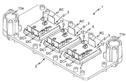
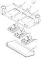
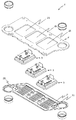
図1、図2及び図4には、本発明に従うパワー半導体装置1が図示されており、図2及び残りの断面図には、パワー半導体装置1の、本発明を理解するために本質的である構成要素のみが図示されている。図3には、冷却プレート5が溶接固定されている第一の冷却ハウジング部材4の斜視図的な背面図が図示されている。図5には、まだ組み立てられていない状態における本発明に従うパワー半導体装置1の斜視図的な前面図が図示されている。本発明に従うパワー半導体装置は、少なくとも一つのパワー半導体モジュール3を有しており、その際、本発明に従うパワー半導体装置は複数のパワー半導体モジュール3を有していてもよく、実施例においては、3つのパワー半導体モジュール3を有している。個々のパワー半導体モジュール3は、電気導電性の導電路13上に配設されているパワー半導体構成要素9を有している。導電路13は、導電的で構造化された第一の導電層13によって形成されている。パワー半導体構成要素9は、有利にははんだ金属層又は焼結金属層を介して、導電層13と導電的に接続されている。個々のパワー半導体構成要素は、有利にはパワー半導体スイッチ又はダイオードの形態で存在する。パワー半導体スイッチは、有利には、例えばIGBTs(絶縁ゲートバイポーラトランジスタ:Insulated Gate Bipolar Transistor)又はMOSFTs(金属酸化膜半導体電界効果トランジスタ:Metal Oxide Semiconductor Field Effect Transistor)のような、トランジスタの形態で存在する。個々のパワー半導体モジュール3は、有利には第一の直流電圧負荷電流端子要素(first DC voltage load current terminal element)DC+、及び、第二の直流電圧負荷電流端子要素(second DC voltage load current terminal element)DC−、及び、交流負荷端子要素(AC load terminal element)ACを有しており、それらは有利にははんだ金属層又は焼結金属層を介して、第一の導電層31と導電的に接続されている。図示されている実施例の枠内では、個々のパワー半導体モジュール3は、直流電圧負荷電流端子DC+及びDC−の間に供給(チャージ)された直流電圧から、直流負荷端子要素ACにて、交流電圧を発生させる。更に個々のパワー半導体モジュール3は、実施例の枠内で、制御端子要素Sを有し、これはパワー半導体モジュール3のパワー半導体スイッチの制御端子に導電的に接続されている。
1, FIG. 2 and FIG. 4 show a power semiconductor device 1 according to the present invention. FIG. 2 and the remaining cross-sectional views show the power semiconductor device 1 essential for understanding the present invention. Only certain components are shown. FIG. 3 shows a perspective rear view of the first
更に、個々のパワー半導体モジュール3は、非導電性の絶縁層6及び冷却プレート5を有しており、その際、絶縁層6は導電路13及び冷却プレート5の間に配設されている。導電路13は絶縁層6に接続されている。実施例の枠内において、絶縁層6と冷却プレート5の間には、導電性で、有利には非構造化された第二の導電層8が配設されており、これは絶縁層6と接続されている。絶縁層6は、有利にはセラミック体の形態で存在している。第一及び第二の導電層31及び8、及び、絶縁層6は、有利には、銅を直接接合した基板(DCB‐基板)によって、共同で形成されている。
Furthermore, each
この状況において、第一及び第二の導電層が単独の層から又は複数の互いに重なりあった層から構成され得ること、が指摘される。そのため、第一及び/又は第二の導電層は、例えば以下の様な銅層を有し得る、つまり例えば一種の貴金属(例えば銀)から又は複数の貴金属化合物からなる、単独又は複数の被覆層(コーティング)を有する銅層を有し得て、それは例えば、接着促進層及び/又は保護層として利用され得る。 In this situation, it is pointed out that the first and second conductive layers can be composed of a single layer or a plurality of overlapping layers. Therefore, the first and / or the second conductive layer may have, for example, the following copper layer, that is, a single or a plurality of coating layers, for example, composed of a single noble metal (for example, silver) or a plurality of noble metal compounds. It can have a copper layer with (coating), which can be used, for example, as an adhesion promoting layer and / or a protective layer.
冷却プレート5は有利にはアルミニウム(例えばAl 99,5)から構成されており、また、そのパワー半導体構成要素9に向けられた面Cにて単独又は複数の互いに重なりあった層を用いて被覆されていてもよく、この層は例えば、それぞれ接着促進層として、及び/又は、保護層として利用され得る、及び/又は、絶縁層6と冷却プレート5の間の機械的応力を減少させるために利用され得る、なおこの機械的応力は、温度変化の際に、絶縁層6と冷却プレート5の異なる熱膨張率に基いて発生し得るものである。実施例の枠内において、冷却プレート5は、その絶縁層6に向けられた面Cにて、銅層12を用いて被覆されており、それは再び例えば、特には貴金属層(例えば銀)のコーティングを用いて被覆されていてもよい。銅層12は冷却プレート5及び絶縁層6の間、そして特には冷却プレートと第二の導電層8の間に配設されている。第二の導電層8は、好ましくはろう付け層又は焼結層によって、直接、又は、(冷却プレートがそのパワー半導体構成要素に向けられた面にて単独又は複数の互いに重なりあった層を用いて被覆されている場合は)間接的に、冷却プレート5と接続されている。第二の導電層8は、実施例の枠内では、ろう付け層又は焼結層を介して銅層12と接続されている。
The
明瞭性のために、図2では、ろう付け層又は焼結層は図示されていない。更に、層の厚さ及びパワー半導体構成要素の厚さは、寸法的に正確に表されてはいないことを指摘する。 For clarity, the brazing layer or sintered layer is not shown in FIG. Furthermore, it is pointed out that the thickness of the layers and the thickness of the power semiconductor components are not accurately represented in dimensions.
この状態において、冷却プレートが絶縁金属基板(IMS)のアルミニウム体の形態で存在してもよいことを指摘する。 It is pointed out that in this state the cooling plate may be present in the form of an aluminum body of an insulated metal substrate (IMS).
冷却プレート5は好ましくは、そのパワー半導体から背けられた面Dに、冷却フィン及び/又は冷却ピン19を有している。
The
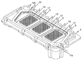
更に、パワー半導体装置1は、液体により貫流可能な冷却体2を有しており、これは第一の冷却ハウジング部材4及び第二の冷却ハウジング部材7を有している。第一の冷却ハウジング部材4は、個々のパワー半導体モジュール3のために、第一の冷却ハウジング部材4を貫通する個々の除去部25(図5参照)を有しており、その際、個々のパワー半導体モジュール3の冷却プレート5は、個々の除去部25内に配設されている。個々の冷却プレート25の一部はその際、個々の除去部25から突出してもよい。個々の冷却プレート5は個々の除去部25を閉じている。第一及び第二の冷却ハウジング部材4及び7は、パワー半導体構成要素9から背けられた冷却プレート5の面Dに空所18が形成されるような、形状を有しており、また、そのように互いに配設されている。第二の冷却ハウジング部材7は、第一の冷却ハウジング部材4と接続されている。液体が冷却体2を貫流しながら、それは空所18を貫流する。冷却プレート5の熱は、液体に伝達され、液体によって排出される。
Furthermore, the power semiconductor device 1 has a
以下においては、パワー半導体モジュール3の配設、及び、パワー半導体モジュール3の第一の冷却ハウジング部材4との接続が、パワー半導体モジュール3の一つを用いて記載されており、その際、その他のパワー半導体モジュール3は、類似の方法で配設され、また、第一の冷却ハウジング部材4と接続されている。
In the following, the arrangement of the
パワー半導体モジュール3の冷却プレート5は、冷却プレート5の周りを取り囲む第一の溶接シーム17を用いて、第一の冷却ハウジング部材4と接続されており、その際、第一の溶接シーム17は、冷却プレート5を第一の冷却ハウジング部材4に対して密封する。第一の溶接シーム17は、冷却プレート5の周りを閉じて取り囲むように延びている。
The
第一の溶接シーム17はその際、有利には冷却プレート5の水平方向の側面15を、除去部25を画定する第一の冷却ハウジング部材4の水平方向の側面16と接続する。
The
第一の溶接シーム17は、有利には空所空間側のみ、すなわち、空所18の面にのみ、配されている。第一の溶接シーム17は、有利にはパワー半導体構成要素から背けられている冷却プレート5の面Dにのみ、配されている。第一の溶接シーム17は、そのような様態では、空所の面からパワー半導体構成要素9に向けられた冷却体2の第一の外側面Aへと、完全に貫いて延びてはいない。これは以下の様な大きな利点、つまり、第一の溶接シーム17を溶接する際に必要となる大きな熱入力が、冷却プレート5のパワー半導体構成要素9から背けられた面Dにて行われるのであって、そして従って、パワー半導体構成要素9の面では行われなれず、それにより、第一の溶接シームの溶接の際に、精密なパワー半導体構成要素9が損傷することを、確実に避けることが出来る、という大きな利点を有している。加えて、冷却プレート5は、溶接の際に分離する液体金属から、パワー半導体スイッチ9及び導電路13を保護する。冷却プレート5は従って、空間的に確実に、溶接プロセスを、パワー半導体構成要素及び導電路から分離する。更に、第一の溶接シームを空所側に配する場合には、冷却プレートと第一の冷却ハウジング部材の間に、空所18からの液体が入り込むことの出来る隙間が残っていないことが保障されている、この液体が隙間内の停滞して残っていたとすると、これは冷却プレート又は第一の冷却ハウジング部材の腐食を導き得る。
The
これと選択的に、図6に図示するように、第一の溶接シーム17は、パワー半導体構成要素に向けられた、冷却体2の第一の外側面Aにのみ接続して配設されていてもよい。第一の溶接シーム17はこの場合、パワー半導体構成要素9に向けられた冷却プレート5の面Cにのみ接続されている。そのような様態では、第一の溶接シーム17は、パワー半導体構成要素9へ向けられた冷却体2の第一の外側面Aから空所18の面へと、完全に貫いて延びてはいない。パワー半導体構成要素9及び導電路13からの溶接プロセスの空間的な分離は、この場合、与えられていない。その代わりとして、第二の冷却ハウジング部材7の第一の冷却ハウジング部材4との接続の後においても、第一の溶接シームの溶接を行うことが出来る、そしてそれは高い柔軟性をもってパワー半導体装置1の製造することを可能とする。
As an alternative, as shown in FIG. 6, the
有利には、除去部25を画定する第一の冷却ハウジング部材4の水平方向の側面16の一部分16aは、冷却プレート5の水平方向の側面15の一部分15aに対応する形状を有している。このために、有利には、冷却プレート5の水平方向の側面15の一部分15aは、パワー半導体構成要素9に向けられた冷却プレート5の主面14に対して、91°から115°または89°から65°の角度αを有し、また、除去部25を画定する第一の冷却ハウジング部材4の水平方向の側面16の一部分16aは、パワー半導体構成要素9に向けられた冷却プレート5の主面14に対して、冷却プレート5の水平方向の側面15の一部分15aのパワー半導体構成要素9に向けられた冷却プレート5の主面14に対する角度αと同じ角度である、角度βを有している。冷却プレート5の水平方向の側面15の一部分15aと除去部25を画定する第一の冷却ハウジング部材4の水平方向の側面16の一部分16aの間には、有利には隙間が形成されている。
Advantageously, the
これと選択的に、例えば冷却プレートの水平方向の側面の一部分が第一の段状形状を有し、また、除去部を画定する第一の冷却ハウジング部材の水平方向の側面の一部分が第一の段状形状に対応する第二の段状形状を有していてもよい。 Optionally, for example, a portion of the horizontal side of the cooling plate has a first stepped shape, and a portion of the horizontal side of the first cooling housing member defining the removal portion is the first. It may have a second step shape corresponding to the step shape.
第一の溶接シーム17の溶接は、有利にはレーザーを用いて行われ、それによって、第一の溶接シーム17は有利にはレーザー溶接シームとして形成されている。選択的に、第一の溶接シーム17の溶接は、例えば電子ビーム溶接を用いて行うことも出来ることから、それにより、第一の溶接シーム17は、電子ビーム溶接シームとして形成されていてもよい。更に選択的に、第一の溶接シーム17の溶接は、例えば摩擦攪拌溶接(摩擦攪拌接合)を用いて行うことも出来ることから、第一の溶接シーム17は摩擦攪拌溶接シームとして形成されていてもよい。第一の溶接シームを形成するために、その他の溶接方法が利用可能であることは自明である。
The welding of the
冷却プレート5は有利には空所18内で延伸する冷却フィン及び/又は冷却ピン19を有している。
The
有利には、第二の冷却ハウジング7は、第二の冷却ハウジング7の周りを取り囲む第二の溶接シーム22を用いて、第一の冷却ハウジング部材4と接続されており、その際、第二の溶接シーム22は第二の冷却ハウジング部材7を第一の冷却ハウジング部材4に対して密閉する。第二の溶接シーム22は第二の冷却ハウジング部材7の周りを閉じて取り囲むように延びている。
Advantageously, the
図1から6に従う実施例の枠内では、第一の冷却ハウジング部材4は第二の冷却ハウジング部材7を水平方向で取り囲んでおり、その際、第二の溶接シーム22は、第二の冷却ハウジング部材7の水平方向の側面20を、第一の冷却ハウジング部材4の水平方向において内側に位置する側面21と接続する。第一の冷却ハウジング部材4は、冷却体2の水平方向の外壁(側壁)を形成する。第二の溶接シーム22は、パワー半導体構成要素9から背けられた冷却体2の外面Bに配設されている。第二の溶接シーム22は、そのような様態において、パワー半導体構成要素9に向けられた冷却体の第一の外面Aの反対側に位置する冷却体の第二の外面Bに配設されている。
Within the frame of the embodiment according to FIGS. 1 to 6, the first
第二の溶接シーム22の溶接は、有利にはレーザーを用いて行われるので、第二の溶接シーム22は有利にはレーザー溶接シームとして形成されている。選択的に、第二の溶接シーム22の溶接は、例えば電子ビーム溶接を用いて行うことも出来ることから、それにより、第二の溶接シーム22は電子ビーム溶接シームとして形成されていてもよい。更に選択的に、第二の溶接シーム22の溶接は、例えば摩擦攪拌溶接を用いて行うことも出来ることから、第二の溶接シーム22は摩擦攪拌溶接シームとして形成されていてもよい。第二の溶接シームを形成するために、その他の溶接方法が利用可能であることは自明である。
Since the welding of the
第二の冷却ハウジング部材7は、有利には、そのパワー半導体構成要素9から背けられた面に、冷却フィン及び/又は冷却ピン24を有している。
The second
冷却体2は、更に有利には、液体往流流入開口部10a、及び、液体往流流入開口部10aに対して一直線上に配設された液体往流流出開口部10b、並びに、液体復流流入開口部11a、及び、液体復流流入開口部11aに対して一直線上に配設された液体往流流出開口部10b、を有している。パワー半導体装置の駆動時には、液体(例えば水)は、パワー半導体構成要素9を冷却するため、冷却体2の液体往流流入開口部10aに流れこむ。液体の一部は、液体往流流出開口部10bを通って再び冷却体2から流れ、また、液体の残りの一部は冷却体2を通って、また特には空所18を通って貫流し、そして、液体往流流出開口部10bにて再び冷却体2から流れ出る。空所18内への及び空所18からの液体の流入及び流出は、連絡路を介して行われる、なお、図3では一つの連絡路23のみが視認できる。液体往流流入開口部10a、液体往流流出開口部10b、液体復流流入開口部11a、及び、液体復流流出開口部11bの配置は、パワー半導体装置システムに対して、複数の冷却体2を、或いは、複数の本願発明に従うパワー半導体装置1を、次々に並べて配設することを可能にする、その際、冷却体の個々に割り当てられた液体開口部は互いに接続されている。
More preferably, the cooling
図7、図8、及び、図10には、本発明に従う更なるパワー半導体装置1´が表されており、図8では、本発明を理解するために、パワー半導体装置1´の本質的な構成要素のみが表されている。図9には、冷却プレート5が溶接固定されている第一の冷却ハウジング部材4´の斜視図的背面図が表されている。図11には、未だに組み立てられていない状態のパワー半導体装置1´が表されている。パワー半導体装置1´はその際、パワー半導体装置1と同様に組み立てられ、第一及び第二の冷却ハウジング部材4´及び7´は、第一及び第二の冷却ハウジング部材4及び7とは変更された様態で、形成されている。図7から図11においては、同一の構成要素に対しては、図1から図6と同一の符号が付されている。パワー半導体装置1´においては、第二の冷却ハウジング部材7´は、第一の冷却ハウジング部材4´から遠ざかるように突出する胴部28を有しており、その際、第二の溶接シーム22´は、第二の冷却部材7´の水平方向の側面20を、パワー半導体構成要素9から背けられている第一の冷却部材4´の第一主面29と、接続する。第一の冷却ハウジング部材4´は、第二の冷却ハウジング部材7´を水平方向で包囲してはいない。第二の冷却ハウジング部材7´は、パワー半導体構成要素9から遠ざかる方向で、第一の冷却ハウジング部材4´に並んで配設されている。
7, 8 and 10 show a further power semiconductor device 1 ′ according to the present invention. In FIG. 8, in order to understand the present invention, the essentials of the power semiconductor device 1 ′ are shown. Only the components are represented. FIG. 9 shows a perspective rear view of the first
この状態において、第一の冷却ハウジング部材が、有利にはアルミニウム(例えばAl99,5)から、又は、有利には例えばAlSi10Mg−FやAlMg4,5Mnといったアルミニウム合金から、構成されること、が指摘される。更に、第二の冷却ハウジング部材が、有利にはアルミニウム(例えばAl99,5)から、又は、有利には例えばAlSi10Mg−FやAlMg4,5Mnといったアルミニウム合金から、構成されること、が指摘される。有利にはアルミニウム又はアルミニウム合金は、少なくともそれぞれの溶接シームの領域において、孔が僅かであるか、孔がない状態であることが望ましい。第一及び/又は第二の冷却ハウジング部材は各々、例えば鋳造された部材の形態、又は例えば深絞り加工された部材の形態であってもよい。 In this state, it is pointed out that the first cooling housing member is preferably composed of aluminum (for example Al99,5) or advantageously from an aluminum alloy, for example AlSi10Mg-F or AlMg4,5Mn. The Furthermore, it is pointed out that the second cooling housing member is preferably composed of aluminum (for example Al99,5) or advantageously from an aluminum alloy, for example AlSi10Mg-F or AlMg4,5Mn. Advantageously, the aluminum or aluminum alloy should have few or no holes, at least in the area of each weld seam. Each of the first and / or second cooling housing members may be, for example, in the form of a cast member or, for example, in the form of a deep drawn member.
更に、第一及び第二の冷却ハウジング部材がそれぞれ、一体的に形成されていてもよいこと、又は、それぞれが互いに接続された部分から形成されていてもよい、ことが指摘される。 Furthermore, it is pointed out that the first and second cooling housing members may each be formed integrally, or may each be formed from portions connected to each other.
更に、有利には、第一の溶接シームと隣接している冷却プレートの側面領域と第一の溶接シームと隣接している第一の冷却ハウジング部材の側面領域とが互いに同一平面上で配設されていることが指摘される。第一の溶接シームと隣接している冷却プレートの側面領域、及び、第一の溶接シームと隣接している第一の冷却ハウジング部材の側面領域は、有利には、絶縁層に対して平行に延伸している。 Further, advantageously, the side area of the cooling plate adjacent to the first weld seam and the side area of the first cooling housing member adjacent to the first weld seam are arranged on the same plane. It is pointed out that The side area of the cooling plate adjacent to the first weld seam and the side area of the first cooling housing member adjacent to the first weld seam are advantageously parallel to the insulating layer. Stretched.
更に、本発明の異なる実施例の特徴を、それらの特徴が互いに排他的でない限り、任意に互いに組み合わせられることは自明であることが指摘される。 It is further pointed out that it is obvious that the features of the different embodiments of the invention can be arbitrarily combined with each other, unless the features are mutually exclusive.
以下においては、本発明に従うパワー半導体装置1或いは1´を製造するための方法について述べられる。 In the following, a method for manufacturing a power semiconductor device 1 or 1 ′ according to the present invention will be described.
第一の方法工程では、電気導電性の導電路13上に配設されているパワー半導体構成要素9を有するパワー半導体モジュール3の準備、及び、第一の冷却ハウジング部材4或いは4´の準備、及び、第二の冷却ハウジング部材7或いは7´の準備が行われ、その際、パワー半導体モジュール3は、非電気導電性の絶縁層6及び冷却プレート5を有しており、絶縁層6は導電路13及び冷却プレート5の間に配設されており、また、第一の冷却ハウジング部材4或いは4´は、第一の冷却ハウジング部材4或いは4´を貫通する除去部25を有している。
In the first method step, the preparation of the
更なる方法工程では、冷却ハウジング部材4或いは4´の除去部25での冷却プレート5の配設が行われる。
In a further method step, the
更なる方法工程では、第一の冷却ハウジング部材4或いは4´との冷却プレート5の溶接が行われ、この溶接は、冷却プレート5の周りを取り囲み、冷却プレート5を第一の冷却ハウジング部材4或いは4´に対して密閉する、第一の溶接シーム17が発生するように行われ、その際、この第一の冷却ハウジング部材4或いは4´との冷却プレート5の溶接は、パワー半導体構成要素9から背けられている冷却プレート5の面Dにて行われる。
In a further method step, the
更なる方法工程では、第一の冷却ハウジング部材4或いは4´に対する第二の冷却ハウジング部材7或いは7´の配設が行われ、その際、この第一の冷却ハウジング部材4或いは4´に対する第二の冷却ハウジング部材7或いは7´の配設は、パワー半導体構成要素9から背けられた冷却プレート5の面Dに空所18が形成されるように行われ、また、第一及び第二の冷却ハウジング部材はそのような形状を有している。
In a further method step, the second
更なる方法工程では、第二の冷却ハウジング部材7或いは7´の第一の冷却ハウジング部材4或いは4´との接続が行われる。有利には、この第二の冷却ハウジング部材7或いは7´の第一の冷却ハウジング部材4或いは4´との接続は、第二の冷却ハウジング部材7或いは7´の第一の冷却ハウジング部材4或いは4´との溶接によるものであり、その際、この第二の冷却ハウジング部材7或いは7´の第一の冷却ハウジング部材4或いは4´との溶接は、第二の冷却ハウジング部材7或いは7´が第二の冷却ハウジング部材7或いは7´の周りを取り囲む第二の溶接シーム22或いは22´を用いて第一の冷却ハウジング部材4或いは4´と接続され、その際第二の溶接シーム22或いは22´が第二の冷却ハウジング部材7或いは7´を第一の冷却ハウジング部材4或いは4´に対して密閉するように、実行される。
In a further method step, the second
1、1´ パワー半導体装置
2 冷却体
3 パワー半導体モジュール
4、4´ 第一の冷却ハウジング部材
5 冷却プレート
6 絶縁層
7、7´ 第二の冷却ハウジング部材
9 パワー半導体構成要素
13 導電路
15、16 水平方向の側面
17 第一の溶接シーム
25 除去部(カットアウト部)
DESCRIPTION OF SYMBOLS 1, 1 '
Claims (15)
前記パワー半導体モジュール(3)が、電気導電性の導電路(13)上に配設されているパワー半導体構成要素(9)を有して、
前記パワー半導体モジュール(3)が非導電性の絶縁層(6)及び冷却プレート(5)を有しており、
前記絶縁層(6)が前記導電路(13)及び前記冷却プレート(5)の間に配設されており、
前記冷却体(2)が、第一の冷却ハウジング部材(4、4´)、及び、第二の冷却ハウジング部材(7、7´)を有しており、前記第一の冷却ハウジング部材(4、4´)は前記第一の冷却ハウジング部材(4、4´)を貫通する除去部(25)を有しており、
前記冷却プレート(5)が前記除去部(25)に配設されており、
前記第一及び第二の冷却ハウジング部材(4、4´、7、7´)が、前記パワー半導体構成要素(9)から背けられた前記冷却体(5)の面(D)に空所(18)が形成されるような形状を有し、また互いにそのように配設されており、
前記冷却プレート(5)が、前記冷却プレート(5)の周りを取り囲む第一の溶接シーム(17)を用いて、前記第一の冷却ハウジング部材(4、4´)と接続されており、
前記第一の溶接シーム(17)が前記冷却プレート(5)を前記第一の冷却ハウジング部材(4、4´)に対して密閉し、
前記第二の冷却ハウジング部材(7、7´)が前記第一の冷却ハウジング部材(4、4´)と接続されていること、
を特徴とするパワー半導体装置。 In the power semiconductor device having the power semiconductor module (3) and the cooling body (2) that can flow through the liquid,
The power semiconductor module (3) has a power semiconductor component (9) disposed on an electrically conductive path (13),
The power semiconductor module (3) has a non-conductive insulating layer (6) and a cooling plate (5);
The insulating layer (6) is disposed between the conductive path (13) and the cooling plate (5);
The cooling body (2) includes a first cooling housing member (4, 4 ') and a second cooling housing member (7, 7'), and the first cooling housing member (4 4 ′) has a removal portion (25) penetrating the first cooling housing member (4, 4 ′),
The cooling plate (5) is disposed in the removal section (25);
The first and second cooling housing members (4, 4 ', 7, 7') are vacant in the surface (D) of the cooling body (5), which is away from the power semiconductor component (9). 18) are formed and arranged so as to each other,
The cooling plate (5) is connected to the first cooling housing member (4, 4 ') using a first welding seam (17) surrounding the cooling plate (5);
The first weld seam (17) seals the cooling plate (5) against the first cooling housing member (4, 4 ');
The second cooling housing member (7, 7 ') is connected to the first cooling housing member (4, 4');
A power semiconductor device.
前記第一の溶接シーム(17)が、前記冷却プレート(5)の水平方向の側面(15)を、前記除去部(25)を画定する前記第一の冷却ハウジング部材(4、4´)の水平方向の側面(16)と接続することを特徴とするパワー半導体装置。 The power semiconductor device according to claim 1,
The first weld seam (17) defines a horizontal side surface (15) of the cooling plate (5) of the first cooling housing member (4, 4 ') that defines the removal portion (25). A power semiconductor device connected to a side surface (16) in a horizontal direction.
前記第一の溶接シーム(17)が空所側に配されていることを特徴とするパワー半導体装置。 The power semiconductor device according to claim 1 or 2,
The power semiconductor device according to claim 1, wherein the first welding seam (17) is disposed on the void side.
前記第一の溶接シーム(17)が、前記パワー半導体構成要素(9)に向けられた前記冷却体(2)の第一外面(A)に配されていることを特徴とするパワー半導体装置。 The power semiconductor device according to claim 1 or 2,
The power semiconductor device, wherein the first welding seam (17) is arranged on a first outer surface (A) of the cooling body (2) directed to the power semiconductor component (9).
前記除去部(25)を画定する前記第一の冷却ハウジング部材(4)の水平方向の側面(16)の一部(16a)が、前記冷却プレート(5)の水平方向の前記側面(15)の一部(15a)に対応する形状を有ることを特徴とするパワー半導体装置。 In the power semiconductor device according to any one of claims 1 to 4,
A portion (16a) of the horizontal side surface (16) of the first cooling housing member (4) defining the removal portion (25) is the horizontal side surface (15) of the cooling plate (5). A power semiconductor device having a shape corresponding to a part (15a).
前記冷却プレート(5)の水平方向の前記側面(15)の前記一部(15a)が、前記パワー半導体構成要素(9)に向けられた前記冷却プレート(5)の主面(14)に対して、91°から115°または89°から65°の角度(α)を有すること、及び、
前記除去部(25)を画定する前記第一の冷却ハウジング部材(4、4´)の水平方向の前記側面(16)の前記一部(16a)が、前記パワー半導体構成要素(9)に向けられた前記冷却プレート(5)の前記主面(14)に対して、前記冷却プレート(5)の水平方向の前記側面(15)の前記一部(15a)の前記パワー半導体構成要素(9)に向けられた前記冷却プレート(5)の前記主面(14)に対する角度(α)と同一の角度(β)を有すること
を特徴とするパワー半導体装置。 The power semiconductor device according to claim 5,
The part (15a) of the side surface (15) in the horizontal direction of the cooling plate (5) is against the main surface (14) of the cooling plate (5) directed to the power semiconductor component (9). Having an angle (α) of 91 ° to 115 ° or 89 ° to 65 °, and
The part (16a) of the horizontal side surface (16) of the first cooling housing member (4, 4 ') defining the removal portion (25) is directed to the power semiconductor component (9). The power semiconductor component (9) of the part (15a) of the side surface (15) in the horizontal direction of the cooling plate (5) with respect to the main surface (14) of the cooling plate (5) formed A power semiconductor device having the same angle (β) as the angle (α) of the cooling plate (5) directed to the main surface (14).
前記冷却プレート(5)が前記空所(18)内で延びる冷却フィン及び/又は冷却ピン(19)を有することを特徴とするパワー半導体装置。 In the power semiconductor device according to any one of claims 1 to 6,
The power semiconductor device, wherein the cooling plate (5) has cooling fins and / or cooling pins (19) extending in the void (18).
前記第一の溶接シーム(17、17´)が、レーザー溶接シーム、電子ビーム溶接シーム、又は、摩擦攪拌溶接シームとして形成されていることを特徴とするパワー半導体装置。 In the power semiconductor device according to any one of claims 1 to 7,
The power semiconductor device, wherein the first welding seam (17, 17 ') is formed as a laser welding seam, an electron beam welding seam, or a friction stir welding seam.
前記第二の冷却ハウジング部材(7、7´)が、前記第二の冷却ハウジング部材(7、7´)の周りを取り囲む第二の溶接シーム(22、22´)を用いて、前記第一の冷却ハウジング部材(4、4´)に接続されており、その際、前記第二の溶接シーム(22、22´)が前記第二の冷却ハウジング部材(7、7´)を前記第一の冷却ハウジング部材(4、4´)に対して密閉することを特徴とするパワー半導体装置。 In the power semiconductor device according to any one of claims 1 to 8,
The second cooling housing member (7, 7 ') uses the second welding seam (22, 22') surrounding the second cooling housing member (7, 7 ') to The second cooling seam (22, 22 ') connects the second cooling housing member (7, 7') to the first cooling housing member (4, 4 '). A power semiconductor device, wherein the power semiconductor device is sealed against a cooling housing member (4, 4 ').
前記第一の冷却ハウジング部材(4)が、前記第二の冷却ハウジング部材(7)を水平方向で取り囲み、その際、前記第二の溶接シーム(22)が、前記第二の冷却ハウジング部材(7)の水平方向の側面(20)を、前記第一の冷却ハウジング部材(4)の水平方向内側に存する側面(21)と接続することを特徴とするパワー半導体装置。 The power semiconductor device according to claim 9, wherein
The first cooling housing member (4) surrounds the second cooling housing member (7) in the horizontal direction, wherein the second welding seam (22) is connected to the second cooling housing member ( 7) A power semiconductor device characterized in that the horizontal side surface (20) of 7) is connected to the side surface (21) existing inside the horizontal direction of the first cooling housing member (4).
第二の溶接シーム(22)が、前記パワー半導体構成要素(9)から背けられた前記冷却体(2)の前記第二の外側面(B)に、配設されていることを特徴とするパワー半導体装置。 The power semiconductor device according to claim 10,
A second weld seam (22) is disposed on the second outer surface (B) of the cooling body (2), which is turned away from the power semiconductor component (9). Power semiconductor device.
前記第二の冷却ハウジング部材(7´)が、前記第一の冷却ハウジング部材(4´)から遠ざかるように突出する胴部(28)を有し、その際、前記第二の溶接シーム(22´)が、前記第二の冷却ハウジング部材(7´)の水平方向の前記側面(20)を、前記パワー半導体構成要素(9)から背けられた前記第一の冷却ハウジング部材(4´)の第一主面(29)と接続することを特徴とするパワー半導体装置。 The power semiconductor device according to any one of claims 9 to 11,
The second cooling housing member (7 ') has a body portion (28) projecting away from the first cooling housing member (4'), wherein the second welding seam (22 ′) Of the first cooling housing member (4 ′) facing away from the power semiconductor component (9) the lateral side surface (20) of the second cooling housing member (7 ′). A power semiconductor device connected to the first main surface (29).
前記第二の溶接シーム(22、22´)が、レーザー溶接シーム、電子ビーム溶接シーム、又は、摩擦攪拌溶接シームとして形成されていること
ことを特徴とするパワー半導体装置。 The power semiconductor device according to any one of claims 9 to 12,
The power semiconductor device, wherein the second welding seam (22, 22 ') is formed as a laser welding seam, an electron beam welding seam, or a friction stir welding seam.
a)電気導電性の導電路(13)上に配設されているパワー半導体構成要素(9)を有するパワー半導体モジュール(3)の準備、及び、第一の冷却ハウジング部材(4、4´)の準備、及び、前記第二の冷却ハウジング部材(7、7´)の準備が行われ、その際、前記パワー半導体モジュール(3)が、非電気導電性の絶縁層(6)及び冷却プレート(5)を有しており、前記絶縁層(6)は前記導電路(13)及び前記冷却プレート(5)の間に配設されており、また、前記第一の冷却ハウジング部材(4、4´)は、前記第一の冷却ハウジング部材(4、4´)を貫通する除去部(25)を有していること、
b)前記第一の冷却ハウジング部材(4、4´)の前記除去部(25)内への、前記冷却プレート(5)の配設が行われること、
c)前記冷却プレート(5)の前記第一の冷却ハウジング部材(4、4´)との溶接が、前記冷却プレート(5)の周りを取り囲み、前記冷却プレート(5)を前記第一の冷却ハウジング部材(4、4´)に対して密閉する、第一の溶接シーム(17)が発生するように行われ、その際、前記冷却プレート(5)の前記第一の冷却ハウジング部材(4、4´)との当該溶接が、パワー半導体構成要素(9)から背けられている前記冷却プレート(5)の面(D)にて行われること、
d)前記第一の冷却ハウジング部材(4、4´)に対する前記第二の冷却ハウジング部材(7、7´)の配設が行われ、その際、前記第一の冷却ハウジング部材(4、4´)に対する前記第二の冷却ハウジング部材(7、7´)の当該配設が、前記パワー半導体構成要素(9)から背けられた前記冷却プレート(5)の面(D)に空所(18)が形成されるように、行われ、また、前記第一及び第二の冷却ハウジング部材(4、4´、7、7´)がそのような形状を有していること、及び
e)前記第二の冷却ハウジング部材(7、7´)の前記第一の冷却ハウジング部材(4、4´)との接続が行われること
を特徴とする方法。 The method for manufacturing a power semiconductor device has the following method steps:
a) Preparation of a power semiconductor module (3) having a power semiconductor component (9) disposed on an electrically conductive conductive path (13) and a first cooling housing member (4, 4 ') And the preparation of the second cooling housing member (7, 7 '), in which case the power semiconductor module (3) includes a non-electrically conductive insulating layer (6) and a cooling plate ( 5), and the insulating layer (6) is disposed between the conductive path (13) and the cooling plate (5), and the first cooling housing member (4, 4). ′) Has a removal portion (25) penetrating the first cooling housing member (4, 4 ′),
b) disposing the cooling plate (5) in the removal portion (25) of the first cooling housing member (4, 4 ');
c) welding of the cooling plate (5) to the first cooling housing member (4, 4 ') surrounds the cooling plate (5), and the cooling plate (5) is The first welded seam (17) is hermetically sealed against the housing member (4, 4 '), wherein the first cooling housing member (4, 4 ′) is performed on the surface (D) of the cooling plate (5) facing away from the power semiconductor component (9),
d) Arrangement of the second cooling housing member (7, 7 ') with respect to the first cooling housing member (4, 4') is carried out, in which case the first cooling housing member (4, 4 ') The arrangement of the second cooling housing member (7, 7 ') with respect to ′) is provided in a cavity (18) on the surface (D) of the cooling plate (5) facing away from the power semiconductor component (9). And the first and second cooling housing members (4, 4 ', 7, 7') have such a shape, and e) the A method wherein a second cooling housing member (7, 7 ') is connected to said first cooling housing member (4, 4').
前記第二の冷却ハウジング部材(7、7´)の前記第一の冷却ハウジング部材(4、4´)との接続が、前記第二の冷却ハウジング部材(7、7´)の前記第一の冷却ハウジング部材(4、4´)との溶接によって、行われ、前記第二の冷却ハウジング部材(7、7´)の前記第一の冷却ハウジング部材(4、4´)との当該溶接が、前記第二の冷却ハウジング部材(7、7´)が前記第二の冷却ハウジング部材(7、7´)の周りを取り囲む前記第二の溶接シーム(22、22´)を用いて前記第一の冷却ハウジング部材(4、4´)と接続され、その際前記第二の溶接シーム(22、22´)が前記第二の冷却ハウジング部材(7、7´)を前記第一の冷却ハウジング部材(4、4´)に対して密閉するように、実行されること、
と特徴とする方法。 15. The method of claim 14, wherein
The connection of the second cooling housing member (7, 7 ') to the first cooling housing member (4, 4') is the first cooling housing member (7, 7 '). The welding of the second cooling housing member (7, 7 ') to the first cooling housing member (4, 4') by welding to the cooling housing member (4, 4 '), The second cooling housing member (7, 7 ') surrounds the second cooling housing member (7, 7') using the second welding seam (22, 22 '). Connected to the cooling housing member (4, 4 '), wherein the second welding seam (22, 22') connects the second cooling housing member (7, 7 ') to the first cooling housing member ( 4, 4 ′) to be sealed against
And a method characterized.
Applications Claiming Priority (2)
| Application Number | Priority Date | Filing Date | Title |
|---|---|---|---|
| DE102013109589.5 | 2013-09-03 | ||
| DE201310109589 DE102013109589B3 (en) | 2013-09-03 | 2013-09-03 | Power semiconductor device and method for producing a power semiconductor device |
Publications (1)
| Publication Number | Publication Date |
|---|---|
| JP2015050465A true JP2015050465A (en) | 2015-03-16 |
Family
ID=51167798
Family Applications (1)
| Application Number | Title | Priority Date | Filing Date |
|---|---|---|---|
| JP2014176971A Withdrawn JP2015050465A (en) | 2013-09-03 | 2014-09-01 | Power semiconductor device and method of manufacturing power semiconductor device |
Country Status (7)
| Country | Link |
|---|---|
| US (1) | US9111900B2 (en) |
| EP (1) | EP2844051A3 (en) |
| JP (1) | JP2015050465A (en) |
| KR (1) | KR20150026862A (en) |
| CN (1) | CN104425406B (en) |
| DE (1) | DE102013109589B3 (en) |
| IN (1) | IN2014MU02658A (en) |
Cited By (3)
| Publication number | Priority date | Publication date | Assignee | Title |
|---|---|---|---|---|
| JPWO2016203885A1 (en) * | 2015-06-17 | 2017-09-21 | 富士電機株式会社 | Power semiconductor module and cooler |
| JP2017212401A (en) * | 2016-05-27 | 2017-11-30 | 日産自動車株式会社 | Manufacturing method of power converter and cooling structure |
| JP2019110208A (en) * | 2017-12-18 | 2019-07-04 | トヨタ自動車株式会社 | Reactor unit |
Families Citing this family (21)
| Publication number | Priority date | Publication date | Assignee | Title |
|---|---|---|---|---|
| DE102015211160A1 (en) * | 2015-06-17 | 2016-12-22 | Zf Friedrichshafen Ag | Arrangement for cooling a power module |
| DE102015211163A1 (en) * | 2015-06-17 | 2016-12-22 | Zf Friedrichshafen Ag | Arrangement for cooling a power module |
| EP3116292B1 (en) | 2015-07-06 | 2021-03-17 | EDAG Engineering AG | Electronic module with generative cooling body |
| DE102015114188B4 (en) * | 2015-08-26 | 2019-03-07 | Semikron Elektronik Gmbh & Co. Kg | Power electronic submodule with a two-part housing |
| DE102015223413A1 (en) * | 2015-11-26 | 2017-06-01 | Zf Friedrichshafen Ag | Copper-aluminum heat sinks |
| US9824953B1 (en) | 2016-05-16 | 2017-11-21 | Caterpillar Inc. | Mounting and environmental protection device for an IGBT module |
| KR101956983B1 (en) | 2016-09-20 | 2019-03-11 | 현대자동차일본기술연구소 | Power module and manufacturing method therefor |
| DE102017101269B4 (en) | 2017-01-24 | 2019-03-07 | Semikron Elektronik Gmbh & Co. Kg | Power semiconductor device with a power semiconductor module and a heat sink |
| DE102017001351A1 (en) * | 2017-02-11 | 2018-08-16 | Leopold Kostal Gmbh & Co. Kg | Electrical device and method of making an electrical device |
| JP6496845B2 (en) * | 2017-02-13 | 2019-04-10 | 新電元工業株式会社 | Electronics |
| DE102019200142A1 (en) * | 2019-01-08 | 2020-07-09 | Volkswagen Aktiengesellschaft | Cooling unit for removing waste heat from at least one power component |
| DE102019202903A1 (en) * | 2019-03-04 | 2020-09-10 | Abb Schweiz Ag | Electronic converter trained based on welding technologies |
| DE102019202902A1 (en) * | 2019-03-04 | 2020-09-10 | Abb Schweiz Ag | Direct cooling of a converter using an embossed plate |
| CN110173957B (en) * | 2019-06-19 | 2023-09-08 | 广东文轩热能科技股份有限公司 | Novel liquid cooling plate |
| US11562911B2 (en) | 2019-07-25 | 2023-01-24 | Hitachi Energy Switzerland Ag | Power semiconductor module and method of forming the same |
| DE102020207947A1 (en) * | 2019-11-25 | 2021-05-27 | Volkswagen Aktiengesellschaft | Cooling arrangement for electronic components of a motor vehicle and manufacturing method therefor |
| DE102020110937B4 (en) | 2020-04-22 | 2022-06-09 | Semikron Elektronik Gmbh & Co. Kg | Cooling device for cooling a power semiconductor module |
| DE102020111528A1 (en) * | 2020-04-28 | 2021-10-28 | Semikron Elektronik Gmbh & Co. Kg | Power electronic arrangement with a multi-phase power semiconductor module |
| CN114206064A (en) * | 2020-09-02 | 2022-03-18 | 春鸿电子科技(重庆)有限公司 | Liquid cooling head and manufacturing method thereof |
| CN114361122A (en) * | 2021-08-11 | 2022-04-15 | 华为技术有限公司 | Packaging structure and packaging method of power module |
| DE102022201557B3 (en) | 2022-02-15 | 2023-07-20 | Magna powertrain gmbh & co kg | Power module assembly and assembly method for the power module assembly |
Family Cites Families (9)
| Publication number | Priority date | Publication date | Assignee | Title |
|---|---|---|---|---|
| US5323292A (en) * | 1992-10-06 | 1994-06-21 | Hewlett-Packard Company | Integrated multi-chip module having a conformal chip/heat exchanger interface |
| US5514906A (en) * | 1993-11-10 | 1996-05-07 | Fujitsu Limited | Apparatus for cooling semiconductor chips in multichip modules |
| JP3946018B2 (en) * | 2001-09-18 | 2007-07-18 | 株式会社日立製作所 | Liquid-cooled circuit device |
| WO2005088714A1 (en) * | 2004-03-08 | 2005-09-22 | Remmele Engineering, Inc. | Cold plate and method of making the same |
| US7071552B2 (en) * | 2004-03-29 | 2006-07-04 | Intel Corporation | IC die with directly bonded liquid cooling device |
| JP4600199B2 (en) * | 2005-07-29 | 2010-12-15 | 三菱マテリアル株式会社 | Cooler and power module |
| US8369090B2 (en) * | 2009-05-12 | 2013-02-05 | Iceotope Limited | Cooled electronic system |
| DE102010043446B3 (en) | 2010-11-05 | 2012-01-12 | Semikron Elektronik Gmbh & Co. Kg | Performance semiconductor system |
| US10269682B2 (en) * | 2015-10-09 | 2019-04-23 | Taiwan Semiconductor Manufacturing Company, Ltd. | Cooling devices, packaged semiconductor devices, and methods of packaging semiconductor devices |
-
2013
- 2013-09-03 DE DE201310109589 patent/DE102013109589B3/en active Active
-
2014
- 2014-07-14 EP EP14176903.4A patent/EP2844051A3/en not_active Withdrawn
- 2014-08-19 IN IN2658MU2014 patent/IN2014MU02658A/en unknown
- 2014-08-22 KR KR20140109594A patent/KR20150026862A/en not_active Application Discontinuation
- 2014-09-01 JP JP2014176971A patent/JP2015050465A/en not_active Withdrawn
- 2014-09-03 CN CN201410446027.3A patent/CN104425406B/en active Active
- 2014-09-03 US US14/476,299 patent/US9111900B2/en not_active Expired - Fee Related
Cited By (4)
| Publication number | Priority date | Publication date | Assignee | Title |
|---|---|---|---|---|
| JPWO2016203885A1 (en) * | 2015-06-17 | 2017-09-21 | 富士電機株式会社 | Power semiconductor module and cooler |
| US10304756B2 (en) | 2015-06-17 | 2019-05-28 | Fuji Electric Co., Ltd. | Power semiconductor module and cooler |
| JP2017212401A (en) * | 2016-05-27 | 2017-11-30 | 日産自動車株式会社 | Manufacturing method of power converter and cooling structure |
| JP2019110208A (en) * | 2017-12-18 | 2019-07-04 | トヨタ自動車株式会社 | Reactor unit |
Also Published As
| Publication number | Publication date |
|---|---|
| IN2014MU02658A (en) | 2015-10-09 |
| CN104425406A (en) | 2015-03-18 |
| DE102013109589B3 (en) | 2015-03-05 |
| US9111900B2 (en) | 2015-08-18 |
| US20150061112A1 (en) | 2015-03-05 |
| EP2844051A2 (en) | 2015-03-04 |
| KR20150026862A (en) | 2015-03-11 |
| EP2844051A3 (en) | 2016-06-01 |
| CN104425406B (en) | 2019-01-08 |
Similar Documents
| Publication | Publication Date | Title |
|---|---|---|
| JP2015050465A (en) | Power semiconductor device and method of manufacturing power semiconductor device | |
| US8421235B2 (en) | Semiconductor device with heat spreaders | |
| JP6234630B2 (en) | Power module | |
| JP6300633B2 (en) | Power module | |
| US9520305B2 (en) | Power semiconductor arrangement and method of producing a power semiconductor arrangement | |
| US10279653B2 (en) | Power converter | |
| US9852962B2 (en) | Waterproof electronic device and manufacturing method thereof | |
| JPWO2014045766A1 (en) | Semiconductor device and manufacturing method of semiconductor device | |
| WO2013088864A1 (en) | Semiconductor device | |
| US10818573B2 (en) | Power semiconductor module with heat dissipation plate | |
| JP2008042074A (en) | Semiconductor device and power conversion device | |
| CN102187456A (en) | Semiconductor device cooling structure and power converter provided with the cooling structure | |
| TW201533857A (en) | Semiconductor device | |
| JP2018081980A (en) | Semiconductor device | |
| JP2012064677A (en) | Semiconductor module | |
| JP2009076592A (en) | Method of crimping electrode of semiconductor device and heat slinger | |
| JP6919392B2 (en) | Semiconductor module | |
| JP2011115020A (en) | Power unit | |
| JP2009164647A (en) | Semiconductor device | |
| JP5217015B2 (en) | Power converter and manufacturing method thereof | |
| CN111373850A (en) | Power module | |
| JP2010062491A (en) | Semiconductor device and composite semiconductor device | |
| JP7131708B2 (en) | semiconductor equipment | |
| JP2018032835A (en) | Semiconductor device manufacturing method | |
| JP7074046B2 (en) | Semiconductor devices and their manufacturing methods |
Legal Events
| Date | Code | Title | Description |
|---|---|---|---|
| A621 | Written request for application examination |
Free format text: JAPANESE INTERMEDIATE CODE: A621 Effective date: 20170614 |
|
| A761 | Written withdrawal of application |
Free format text: JAPANESE INTERMEDIATE CODE: A761 Effective date: 20170919 |
|
| A521 | Request for written amendment filed |
Free format text: JAPANESE INTERMEDIATE CODE: A821 Effective date: 20170919 |