JP2015012015A - Processing method of wafer - Google Patents
Processing method of wafer Download PDFInfo
- Publication number
- JP2015012015A JP2015012015A JP2013133926A JP2013133926A JP2015012015A JP 2015012015 A JP2015012015 A JP 2015012015A JP 2013133926 A JP2013133926 A JP 2013133926A JP 2013133926 A JP2013133926 A JP 2013133926A JP 2015012015 A JP2015012015 A JP 2015012015A
- Authority
- JP
- Japan
- Prior art keywords
- wafer
- modified layer
- crack
- reference width
- width
- Prior art date
- Legal status (The legal status is an assumption and is not a legal conclusion. Google has not performed a legal analysis and makes no representation as to the accuracy of the status listed.)
- Granted
Links
- 238000003672 processing method Methods 0.000 title claims abstract description 21
- 230000001681 protective effect Effects 0.000 claims abstract description 26
- 230000001678 irradiating effect Effects 0.000 claims abstract description 8
- 238000000034 method Methods 0.000 claims description 2
- 230000015572 biosynthetic process Effects 0.000 abstract description 6
- 239000010410 layer Substances 0.000 description 119
- 235000012431 wafers Nutrition 0.000 description 99
- 230000002093 peripheral effect Effects 0.000 description 4
- 239000000758 substrate Substances 0.000 description 4
- 238000003754 machining Methods 0.000 description 3
- 238000010521 absorption reaction Methods 0.000 description 2
- 238000001514 detection method Methods 0.000 description 2
- 238000003384 imaging method Methods 0.000 description 2
- 239000004065 semiconductor Substances 0.000 description 2
- XUIMIQQOPSSXEZ-UHFFFAOYSA-N Silicon Chemical compound [Si] XUIMIQQOPSSXEZ-UHFFFAOYSA-N 0.000 description 1
- 229910009372 YVO4 Inorganic materials 0.000 description 1
- 239000012790 adhesive layer Substances 0.000 description 1
- 238000000149 argon plasma sintering Methods 0.000 description 1
- 238000010586 diagram Methods 0.000 description 1
- 239000011521 glass Substances 0.000 description 1
- 239000000463 material Substances 0.000 description 1
- 239000002184 metal Substances 0.000 description 1
- 239000011347 resin Substances 0.000 description 1
- 229920005989 resin Polymers 0.000 description 1
- 229910052710 silicon Inorganic materials 0.000 description 1
- 239000010703 silicon Substances 0.000 description 1
- 238000002834 transmittance Methods 0.000 description 1
Images


Abstract
Description
本発明は、ウェーハの内部にレーザー光線を集光させて分割の起点となる改質層を形成するウェーハの加工方法に関する。 The present invention relates to a wafer processing method in which a laser beam is condensed inside a wafer to form a modified layer serving as a starting point of division.
表面にデバイスが形成されたウェーハを複数のチップに分割するために、ウェーハの内部にレーザー光線を集光させて分割の起点となる改質層を形成するウェーハの加工方法が提案されている(例えば、特許文献1、特許文献2参照)。 In order to divide a wafer having devices formed on the surface into a plurality of chips, a wafer processing method has been proposed in which a laser beam is condensed inside the wafer to form a modified layer serving as a starting point of the division (for example, , See Patent Document 1 and Patent Document 2).
この加工方法では、ウェーハに吸収され難い波長のレーザー光線を、ウェーハの内部に集光させるように分割予定ラインに沿って照射して、多光子吸収による改質層を形成する。改質層が形成されたウェーハに応力を加えることで、ウェーハは分割予定ラインに沿って分割される。 In this processing method, a laser beam having a wavelength that is difficult to be absorbed by the wafer is irradiated along the planned dividing line so as to be condensed inside the wafer, thereby forming a modified layer by multiphoton absorption. By applying a stress to the wafer on which the modified layer is formed, the wafer is divided along the division line.
ところで、上述の加工方法では、ウェーハの深さ方向における改質層の形成位置やレーザー光線の照射パワーといった改質層の形成条件を適切に設定しないと、ウェーハの分割に適した良好な改質層を形成することができない。 By the way, in the above-described processing method, a good modified layer suitable for dividing a wafer is required unless the modified layer forming conditions such as the formation position of the modified layer in the depth direction of the wafer and the irradiation power of the laser beam are appropriately set. Can not form.
これに対して、良好な改質層を形成できたか否かは、実際にウェーハを分割するまで分からないという問題があった。そのため、改質層の形成条件が適切に設定されていない状態で多数のウェーハを処理してしまい、分割不良を多発させる恐れもある。 On the other hand, there was a problem that it was not known until the wafer was actually divided whether or not a good modified layer could be formed. For this reason, many wafers are processed in a state where the formation conditions of the modified layer are not set appropriately, and there is a possibility that division failures occur frequently.
本発明はかかる問題点に鑑みてなされたものであり、その目的とするところは、改質層の形成条件が適切であるか否かをウェーハの分割前に判定可能なウェーハの加工方法を提供することである。 The present invention has been made in view of such a problem, and an object of the present invention is to provide a wafer processing method capable of determining whether or not the conditions for forming the modified layer are appropriate before dividing the wafer. It is to be.
本発明によれば、ウェーハの表面に複数設定された分割予定ラインに沿って該ウェーハの内部に改質層を形成するウェーハの加工方法であって、該ウェーハの該表面側に保護部材を配設する保護部材配設ステップと、該保護部材配設ステップの後に、該ウェーハの該保護部材側をチャックテーブルで保持する保持ステップと、該ウェーハを透過する波長のレーザー光線を該ウェーハの内部に焦点を合わせつつ照射して形成される改質層の基準幅を設定する基準幅設定ステップと、該基準幅設定ステップの後に、該チャックテーブルに保持された該ウェーハの裏面側から該レーザー光線を該ウェーハの内部に焦点を合わせつつ任意の分割予定ラインに沿って照射し、該ウェーハの内部に該任意の分割予定ラインに沿った該改質層を形成する改質層形成ステップと、該改質層形成ステップの後に、該チャックテーブルに保持された該ウェーハの該改質層を赤外線カメラで該ウェーハの該裏面側から撮像し、撮像された該改質層の幅が該基準幅以上に太い場合、該改質層から該ウェーハの表面に向かって伸長するクラックの発生有りと判定するクラック判定ステップと、を含むことを特徴とするウェーハの加工方法が提供される。 According to the present invention, there is provided a wafer processing method for forming a modified layer inside a wafer along a plurality of division lines set on the surface of the wafer, wherein a protective member is disposed on the surface side of the wafer. A protective member disposing step, a holding step of holding the protective member side of the wafer by a chuck table after the protective member disposing step, and focusing a laser beam having a wavelength transmitting through the wafer inside the wafer. A reference width setting step for setting a reference width of a modified layer formed by irradiating the wafer, and after the reference width setting step, the laser beam is irradiated from the back side of the wafer held on the chuck table. Irradiation along an arbitrary division line while focusing on the inside of the wafer to form the modified layer along the arbitrary division line inside the wafer After the forming step and the modified layer forming step, the modified layer of the wafer held on the chuck table is imaged from the back side of the wafer by an infrared camera, and the width of the imaged modified layer And a crack determination step for determining that a crack extending from the modified layer toward the surface of the wafer is present when the thickness is larger than the reference width. .
また、前記ウェーハの加工方法において、前記基準値設定ステップで設定される該基準幅は、4μmであることが好ましい。 In the wafer processing method, the reference width set in the reference value setting step is preferably 4 μm.
また、前記ウェーハの加工方法において、前記基準幅設定ステップでは、前記ウェーハの前記改質層が形成されていない前記分割予定ラインに沿って前記レーザー光線を照射して前記クラックが伸長しない該改質層を形成し、該改質層の前記幅を前記赤外線カメラで撮像して測定し、該幅を基に前記基準幅を設定し、前記改質層形成ステップでは、該基準幅設定ステップで照射した該レーザー光線と該焦点の位置を入射方向に変化させた該レーザー光線を該改質層に沿って照射し、該分割予定ラインに沿った改質層を該ウェーハの厚さ方向に複数形成することが好ましい。 Further, in the wafer processing method, in the reference width setting step, the modified layer in which the crack is not elongated by irradiating the laser beam along the division line where the modified layer of the wafer is not formed. And measuring the width of the modified layer by imaging with the infrared camera, setting the reference width based on the width, and irradiating in the reference width setting step in the modified layer forming step Irradiating the laser beam with the laser beam and the position of the focal point changed in the incident direction along the modified layer, and forming a plurality of modified layers along the division line in the thickness direction of the wafer. preferable.
ウェーハの分割に適した良好な改質層が形成される条件では、改質層からウェーハの表面へと向かうクラックが発生する。よって、本発明に係るウェーハの加工方法のように、改質層形成ステップの後にクラック判定ステップを実施することで、改質層の形成条件が適切であるか否かをウェーハの分割前に判定できる。 Under the condition that a good modified layer suitable for dividing the wafer is formed, a crack is generated from the modified layer toward the surface of the wafer. Therefore, as in the wafer processing method according to the present invention, by performing the crack determination step after the modified layer forming step, it is determined before dividing the wafer whether or not the modified layer forming conditions are appropriate. it can.
以下、添付図面を参照して、本発明の実施の形態について説明する。本実施の形態に係るウェーハの加工方法は、保護部材配設ステップ(図1参照)、保持ステップ(図2参照)、基準幅設定ステップ、改質層形成ステップ(図3参照)、クラック判定ステップ(図4、図5参照)を含む。 Embodiments of the present invention will be described below with reference to the accompanying drawings. The wafer processing method according to the present embodiment includes a protective member disposing step (see FIG. 1), a holding step (see FIG. 2), a reference width setting step, a modified layer forming step (see FIG. 3), and a crack determining step. (See FIGS. 4 and 5).
保護部材配設ステップでは、ウェーハの表面側に保護部材を配設する。保持ステップでは、保護部材を介してウェーハをレーザー加工装置のチャックテーブルに吸引保持させる。基準幅設定ステップでは、後のクラック判定ステップにおいて判定の基準となる改質層の基準幅を設定する。 In the protective member disposing step, a protective member is disposed on the front surface side of the wafer. In the holding step, the wafer is sucked and held on the chuck table of the laser processing apparatus via the protective member. In the reference width setting step, a reference width of the modified layer that is a reference for determination in the subsequent crack determination step is set.
改質層形成ステップでは、レーザー加工装置のレーザー加工ヘッドからウェーハの裏面側に向けてレーザー光線を照射し、ストリート(分割予定ライン)に沿う改質層を形成する。クラック判定ステップでは、レーザー加工装置の赤外線カメラで撮像された改質層の幅に基づいて改質層からウェーハの表面に向かうクラックの発生の有無を判定する。以下、本実施の形態に係るウェーハの加工方法について詳述する。 In the modified layer forming step, a laser beam is irradiated from the laser processing head of the laser processing apparatus toward the back side of the wafer to form a modified layer along the street (division planned line). In the crack determination step, it is determined whether or not a crack is generated from the modified layer toward the surface of the wafer based on the width of the modified layer imaged by the infrared camera of the laser processing apparatus. Hereinafter, the wafer processing method according to the present embodiment will be described in detail.
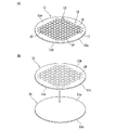
図1(A)は、本実施の形態に係るウェーハの加工方法の対象となるウェーハの構成例を模式的に示す斜視図であり、図1(B)は、保護部材配設ステップを模式的に示す斜視図である。 FIG. 1A is a perspective view schematically showing a configuration example of a wafer that is an object of the wafer processing method according to the present embodiment, and FIG. It is a perspective view shown in FIG.
図1(A)に示すように、本実施の形態の加工方法の対象となるウェーハ11は、円盤状の半導体ウェーハであり、中央のデバイス領域13と、デバイス領域13を囲む外周余剰領域15とを備えている。
As shown in FIG. 1A, a
ウェーハ11の表面11a側のデバイス領域13は、格子状に配列されたストリート(分割予定ライン)17で複数の領域に区画されており、各領域にはIC等のデバイス19が形成されている。ウェーハ11の外周面11cは面取り加工されており、断面形状は円弧状になっている(図3(A)参照)。
The
本実施の形態の加工方法では、まず、このウェーハ11の表面11a側に保護部材を配設する保護部材配設ステップを実施する。図1(B)に示すように、保護部材21は、ウェーハ11と同等の外径を有する円盤状のフィルムであり、表面21a側には接着性のある糊層が設けられている。
In the processing method of the present embodiment, first, a protection member disposing step of disposing a protection member on the
ただし、保護部材21の構成はこれに限定されない。後述する保持ステップ以降のステップにおいてウェーハ11の表面11a側を適切に保護できる部材であれば、保護部材21として使用できる。例えば、ガラス基板、半導体基板、金属基板、樹脂基板等を保護部材21として用いても良い。
However, the structure of the
保護部材配設ステップにおいては、上述したウェーハ11の表面11a側と保護部材21の表面21a側とを対面させるように、ウェーハ11と保護部材21とを位置合わせする。そして、ウェーハ11の表面11a側に保護部材21の表面21aを接触させることでウェーハ11に保護部材21を接着する。
In the protection member disposing step, the
保護部材配設ステップの後には、ウェーハ11に貼着された保護部材21をレーザー加工装置のチャックテーブルに吸引保持させる保持ステップを実施する。図2は、本実施の形態で用いられるレーザー加工装置の構成例を模式的に示す斜視図である。図2に示すように、レーザー加工装置2は、各構成を支持する基台4を備えている。基台4は、直方体状の基部6と、基部6の後端において上方に延びる壁部8とを含む。
After the protective member disposing step, a holding step for sucking and holding the
基部6の上面には、保護部材21を介してウェーハ11を吸引保持するチャックテーブル10が配置されている。チャックテーブル10の上方には、ウェーハ11に向けてレーザー光線を照射するレーザー加工ヘッド12が設けられている。また、レーザー加工ヘッド12と隣接する位置には、赤外線カメラ14が設けられている。
On the upper surface of the
チャックテーブル10の下方には、チャックテーブル10を割り出し送り方向(Y軸方向)に移動させるY軸移動機構(割り出し送り機構)16が設けられている。Y軸移動機構16は、基部6の上面に固定されY軸方向に平行な一対のY軸ガイドレール18を備える。
Below the chuck table 10, a Y-axis movement mechanism (index feed mechanism) 16 that moves the chuck table 10 in the index feed direction (Y-axis direction) is provided. The Y-
Y軸ガイドレール18には、Y軸移動テーブル20がスライド可能に設置されている。Y軸移動テーブル20の裏面側(下面側)には、ナット(不図示)が固定されており、このナットには、Y軸ガイドレール18と平行なY軸ボールネジ22が螺合されている。
A Y-axis moving table 20 is slidably installed on the Y-
Y軸ボールネジ22の一端部には、Y軸パルスモータ24が連結されている。Y軸パルスモータ24でY軸ボールネジ22を回転させれば、Y軸移動テーブル20は、Y軸ガイドレール18に沿ってY軸方向に移動する。
A Y-
Y軸移動テーブル20の表面側(上面側)には、チャックテーブル10を加工送り方向(X軸方向)に移動させるX軸移動機構(加工送り機構)26が設けられている。X軸移動機構26は、Y軸移動テーブル20の上面に固定されX軸方向に平行な一対のX軸ガイドレール28を備える。
An X-axis movement mechanism (machining feed mechanism) 26 that moves the chuck table 10 in the machining feed direction (X-axis direction) is provided on the front surface side (upper surface side) of the Y-axis movement table 20. The
X軸ガイドレール28には、X軸移動テーブル30がスライド可能に設置されている。X軸移動テーブル30の裏面側(下面側)には、ナット(不図示)が固定されており、このナットには、X軸ガイドレール28と平行なX軸ボールネジ32が螺合されている。
An X-axis moving table 30 is slidably installed on the
X軸ボールネジ32の一端部には、X軸パルスモータ34が連結されている。X軸パルスモータ34でX軸ボールネジ32を回転させれば、X軸移動テーブル30は、X軸ガイドレール28に沿ってX軸方向に移動する。
An
X軸移動テーブル30の表面側(上面側)には、支持台36が設けられている。支持台36の上部には、チャックテーブル10が配置されている。チャックテーブル10は、支持台36の下方に設けられた回転機構(不図示)と連結されており、Z軸の周りに回転する。
A
チャックテーブル10の表面は、ウェーハ11に貼着された保護部材21の裏面21bを吸引保持する保持面10aとなっている。この保持面10aには、チャックテーブル10の内部に形成された流路(不図示)を通じて吸引源(不図示)の負圧が作用し、保護部材21を吸引する吸引力が発生する。
The front surface of the chuck table 10 is a holding
壁部8の上部前面には、前方に向かって延びる支持アーム38が設けられており、この支持アーム38の先端部には、レーザー加工ヘッド12及び赤外線カメラ14が配置されている。
A
レーザー加工ヘッド12は、レーザー発振器(不図示)で発振されるレーザー光線を、チャックテーブル10に保持されたウェーハ11の内部に集光させる集光器(不図示)を備えている。このレーザー加工ヘッド12は、ウェーハ11の内部に集光させるようにレーザー光線を照射して、多光子吸収による改質層を形成する。
The
赤外線カメラ14は、ウェーハ11に吸収され難い赤外領域の光を検出する撮像素子を備え、ウェーハ11に形成された改質層を裏面11b側から撮像する。撮像された撮像画像は、記憶装置(不図示)に記憶され、必要に応じて制御装置(不図示)等で用いられる。
The
保持ステップでは、上述したレーザー加工装置2のチャックテーブル10に、ウェーハ11に貼着された保護部材21を吸引させる。具体的には、まず、図2に示すように、チャックテーブル10の保持面10aと保護部材21の裏面21b側とを対面させるように位置合わせした状態で、チャックテーブル10上にウェーハ11及び保護部材21を載置する。
In the holding step, the
その後、チャックテーブル10の保持面10aに吸引源の負圧を作用させれば、保護部材21はチャックテーブル10で吸引される。これにより、ウェーハ11は保護部材21を介してチャックテーブル10に吸引保持される。
Thereafter, if the negative pressure of the suction source is applied to the holding
保持ステップの後には、後のクラック判定ステップで用いられる改質層の基準幅をレーザー加工装置2に設定する基準幅設定ステップを実施する。基準幅は、例えば、3μm〜5μmの範囲に設定される。設定された基準幅は、レーザー加工装置2の記憶装置に記憶される。
After the holding step, a reference width setting step for setting the reference width of the modified layer used in the subsequent crack determination step in the
このように、改質層の基準幅を設定することで、後のクラック判定ステップにおいてクラックの発生の有無を判定できるようになる。なお、本実施の形態では、基準幅を4μmに設定する。ただし、本発明はこれに限定されず、基準幅は任意に設定できる。 In this way, by setting the reference width of the modified layer, it is possible to determine whether or not a crack has occurred in a subsequent crack determination step. In the present embodiment, the reference width is set to 4 μm. However, the present invention is not limited to this, and the reference width can be arbitrarily set.
本発明者は、鋭意研究の結果、改質層からウェーハ11の表面11a側へと向かうクラックが発生するように改質層を形成すると、ウェーハ11を適切に分割できることを見出した。このような条件でウェーハ11を適切に分割できるのは、クラックの発生によって、ウェーハ11の分割が誘起されるためと考えられる。
As a result of diligent research, the present inventor has found that the
そして、上述のようなクラックが発生する条件では、クラックが発生しない条件と比較して改質層の幅が太く見えることを発見した。この現象は、クラックにおける光の散乱で、本来の改質層の幅よりも広い範囲で反射率(透過率)が変化するために生じると推察される。つまり、観察される改質層の幅に基づいてクラックの発生の有無を判定することで、改質層が適切な条件で形成されたか否かを確認できる。 And it discovered that the width | variety of a modified layer looks thick on the conditions which the above cracks generate | occur | produce compared with the conditions which a crack does not generate | occur | produce. This phenomenon is presumed to occur because the reflectance (transmittance) changes in a range wider than the width of the original modified layer due to light scattering in the cracks. That is, it can be confirmed whether or not the modified layer has been formed under appropriate conditions by determining the presence or absence of the occurrence of cracks based on the width of the observed modified layer.
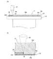
基準幅設定ステップの後には、ウェーハ11のストリート17に沿って改質層を形成する改質層形成ステップを実施する。図3(A)は、改質層形成ステップを模式的に示す一部断面側面図であり、図3(B)は、図3(A)の一部を拡大して示す部分拡大図である。
After the reference width setting step, a modified layer forming step for forming a modified layer along the
図3(A)及び図3(B)に示すように、改質層形成ステップにおいては、まず、チャックテーブル10に保持されたウェーハ11の上方にレーザー加工ヘッド12を位置付ける。そして、チャックテーブル10とレーザー加工ヘッド12とを相対移動させながら、ウェーハ11にレーザビーム40を照射する。
As shown in FIGS. 3A and 3B, in the modified layer forming step, first, the
レーザビーム40は、例えば、YAG、YVO4等をレーザー媒質として発振され、ウェーハ11の裏面11b側に照射される。また、レーザビーム40は、チャックテーブル10とレーザー加工ヘッド12との相対移動により、ストリート17に沿って照射される。レーザビーム40の集光点(焦点)42は、ウェーハ11の内部に位置付けられる。
The
ウェーハ11としてシリコンウェーハを用いる場合には、赤外領域の波長(例えば、1064nm)のレーザビーム40を用いることが好ましい。ウェーハ11に吸収され難い(ウェーハを透過し易い)このような波長のレーザビーム40を用いることで、ウェーハ11の内部に良好な改質層23を形成できる。全てのストリート17に沿って改質層23が形成されると、改質層形成ステップは終了する。
When a silicon wafer is used as the
改質層形成ステップの後には、改質層23からウェーハ11の表面11aに向かうクラックの発生の有無を判定するクラック判定ステップを実施する。図4は、クラック判定ステップを模式的に示す一部断面側面図であり、図5は、クラック判定ステップで撮像される撮像画像の例を模式的に示す画像図である。
After the modified layer forming step, a crack determining step for determining whether or not a crack is generated from the modified
図4(A)及び図4(B)に示すように、クラック判定ステップにおいては、ストリート17に沿って形成された改質層23の上方に赤外線カメラ14を位置付け、裏面11b側からウェーハ11を撮像する。撮像された撮像画像は、レーザー加工装置2の記憶装置に記憶される。
4A and 4B, in the crack determination step, the
赤外線カメラ14は、赤外領域の光を検出する撮像素子を備えているので、赤外線カメラ14でウェーハ11を撮像すると、ウェーハ11の内部の状態を確認できる。本実施の形態では、改質層形成ステップでウェーハ11の内部に改質層23を形成しているので、赤外線カメラ14で撮像された撮像画像には、改質層23が写り込む。
Since the
図4(A)に示すように、適切な条件で改質層23を形成すると、改質層23とウェーハ11の表面11aとの間には、クラック25が発生する。この場合、赤外線カメラ14で撮像される撮像画像は、例えば、図5(A)のようになる。
As shown in FIG. 4A, when the modified
一方、図4(B)に示すように、適切ではない条件で改質層23を形成すると、改質層23とウェーハ11の表面11aとの間には、クラック25が発生しない。この場合、赤外線カメラ14で撮像される撮像画像は、例えば、図5(B)のようになる。
On the other hand, as shown in FIG. 4B, when the modified
図5(A)及び図5(B)の比較から分かるように、クラック25が発生する条件では、クラック25が発生しない条件と比較して改質層23の幅は太く見える。よって、改質層23の幅を、上述の基準幅設定ステップで設定した基準幅と比較することで、改質層23が適切な条件で形成されたか否かを確認できる。
As can be seen from the comparison between FIG. 5A and FIG. 5B, the width of the modified
撮像画像中の改質層23の幅は、例えば、制御装置における画像処理等で検出できる。この場合、例えば、制御装置は、記憶装置に記憶された撮像画像を読み出し、撮像画像中の改質層23の輪郭を抽出することで、改質層23の幅を検出する。
The width of the modified
検出された改質層23の最大幅が基準幅以上の場合、制御装置は、改質層23とウェーハ11の表面11aとの間にクラック25が発生していると判定する。一方、検出された改質層23の最大幅が基準幅未満の場合、制御装置は、改質層23とウェーハ11の表面11aとの間にクラック25が発生していないと判定する。
When the detected maximum width of the modified
すなわち、本実施の形態では、検出された改質層23の最大幅が4μm以上の場合にクラック25が発生していると判定し、検出された改質層23の最大幅が4μm未満の場合にクラック25が発生していないと判定する。なお、ここでは、改質層23の最大幅を基準幅と比較しているが、本発明はこれに限定されない。例えば、改質層23の平均幅等を基準幅と比較しても良い。
That is, in the present embodiment, when the detected maximum width of the modified
ウェーハ11の分割に適した良好な改質層23が形成される条件では、改質層23からウェーハ11の表面11aに向かうクラック25が発生する。よって、本実施の形態に係るウェーハの加工方法のように改質層形成ステップの後にクラック判定ステップを実施することで、改質層23の形成条件が適切であるか否かをウェーハ11の分割前に判定できる。
Under the condition that a good modified
なお、本発明は上記実施の形態の記載に限定されず、種々変更して実施可能である。例えば、上記実施の形態では、改質層の基準幅を任意の値に設定する例を示したが、本発明はこれに限定されない。適切な改質層の基準幅は、改質層が形成される深さや、ウェーハ11の材質等に応じて異なると考えられる。よって、改質層の基準幅を、実測された改質層の幅に基づいて設定しても良い。
In addition, this invention is not limited to description of the said embodiment, A various change can be implemented. For example, in the above-described embodiment, an example in which the reference width of the modified layer is set to an arbitrary value has been shown, but the present invention is not limited to this. It is considered that the appropriate reference width of the modified layer varies depending on the depth at which the modified layer is formed, the material of the
この場合、基準幅設定ステップにおいて、例えば、チャックテーブル10に保持されるウェーハ11のストリート17に沿って、クラック25が発生しないような条件でレーザー光線40を照射し、改質層23を形成する。そして、赤外線カメラ14でウェーハ11の裏面11b側を撮像して、この改質層23の幅を測定する。
In this case, in the reference width setting step, for example, the modified
基準幅としては、例えば、測定された改質層23の幅より僅かに大きい値を設定することが好ましい。このように設定された改質層の基準幅は、実測された改質層23の幅に基づくので、クラック判定ステップにおける判定精度を十分に高めることができる。
As the reference width, for example, a value slightly larger than the measured width of the modified
なお、この場合、後の改質層形成ステップでは、レーザー光線40の集光点(焦点)42の位置を入射方向に変化させて、基準幅設定ステップにおいて形成した改質層23とは異なる高さ位置に改質層23を形成する。つまり、この場合、ストリート17に沿う改質層23は、ウェーハ11の厚み方向に複数形成される。
In this case, in the later modified layer forming step, the position of the condensing point (focal point) 42 of the
また、上記実施の形態では、改質層23の幅の検出、及びクラック25の発生の有無の判定を制御装置において実施する態様を例示しているが、本発明はこれに限定されない。改質層23の幅の検出、及びクラック25の発生の有無の判定は、作業者によって行われても良い。
Moreover, although the embodiment described above illustrates an embodiment in which the detection of the width of the modified
さらに、上記実施の形態では、改質層形成ステップにおいて全てのストリート17に沿う改質層23を形成した後に、クラック25の発生の有無を判定するクラック判定ステップを実施しているが、本発明はこれに限定されない。
Further, in the above-described embodiment, the crack determining step for determining whether or not the
例えば、改質層形成ステップにおいて任意のストリート17に改質層23を形成した後、当該改質層23に対してクラック25の発生の有無を判定するクラック判定ステップを実施しても良い。
For example, after forming the modified
対象のストリート17においてクラック25が発生していると判定された場合には、同じ条件で他のストリート17にも改質層23を形成する。一方、クラック25が発生していないと判定された場合には、条件を変更して改質層23を形成し直す。
If it is determined that the
つまり、任意のストリート17に改質層23を形成する改質層形成ステップ(第1の改質層形成ステップ)を実施した後、クラック25の発生の有無を判定するクラック判定ステップを実施し、クラック25が発生していると判定された場合には、他のストリート17(残りのストリート17)に改質層23を形成する改質層形成ステップ(第2の改質層形成ステップ)を実施する。
That is, after performing the modified layer forming step (first modified layer forming step) for forming the modified
また、任意のストリート17に改質層23を形成する改質層形成ステップ(第1の改質層形成ステップ)を実施した後、クラック25の発生の有無を判定するクラック判定ステップを実施し、クラック25が発生していないと判定された場合には、既に改質層23が形成されている任意のストリート17を含むすべてのストリート17に異なる条件で改質層23を形成する改質層形成ステップ(第3の改質層形成ステップ)を実施する。
In addition, after performing the modified layer forming step (first modified layer forming step) for forming the modified
言い換えれば、全ての改質層23を形成する前にクラック判定ステップを実施する。これにより、改質層23の形成条件が適切であるか否かを全ての改質層23を形成する前に判定できるので、適切でない改質層23の形成条件を早期に発見し、修正できる。
In other words, a crack determination step is performed before all the modified
その他、上記実施の形態に係る構成、方法などは、本発明の目的の範囲を逸脱しない限りにおいて適宜変更して実施できる。 In addition, the configurations, methods, and the like according to the above-described embodiments can be changed as appropriate without departing from the scope of the object of the present invention.
11 ウェーハ
11a 表面
11b 裏面
11c 外周面
13 デバイス領域
15 外周余剰領域
17 ストリート(分割予定ライン)
19 デバイス
21 保護部材
21a 表面
21b 裏面
23 改質層
25 クラック
2 レーザー加工装置
4 基台
6 基部
8 壁部
10 チャックテーブル
12 レーザー加工ヘッド
14 赤外線カメラ
16 Y軸移動機構(割り出し送り機構)
18 Y軸ガイドレール
20 Y軸移動テーブル
22 Y軸ボールネジ
24 Y軸パルスモータ
26 X軸移動機構(加工送り機構)
28 X軸ガイドレール
30 X軸移動テーブル
32 X軸ボールネジ
34 X軸パルスモータ
36 支持台
38 支持アーム
40 レーザー光線
42 集光点(焦点)
DESCRIPTION OF
DESCRIPTION OF
18 Y-axis guide rail 20 Y-axis moving table 22 Y-axis ball screw 24 Y-
28
Claims (3)
該ウェーハの該表面側に保護部材を配設する保護部材配設ステップと、
該保護部材配設ステップの後に、該ウェーハの該保護部材側をチャックテーブルで保持する保持ステップと、
該ウェーハを透過する波長のレーザー光線を該ウェーハの内部に焦点を合わせつつ照射して形成される改質層の基準幅を設定する基準幅設定ステップと、
該基準幅設定ステップの後に、該チャックテーブルに保持された該ウェーハの裏面側から該レーザー光線を該ウェーハの内部に焦点を合わせつつ任意の分割予定ラインに沿って照射し、該ウェーハの内部に該任意の分割予定ラインに沿った該改質層を形成する改質層形成ステップと、
該改質層形成ステップの後に、該チャックテーブルに保持された該ウェーハの該改質層を赤外線カメラで該ウェーハの該裏面側から撮像し、撮像された該改質層の幅が該基準幅以上に太い場合、該改質層から該ウェーハの表面に向かって伸長するクラックの発生有りと判定するクラック判定ステップと、を含むことを特徴とするウェーハの加工方法。 A wafer processing method for forming a modified layer inside a wafer along a plurality of scheduled division lines set on the surface of the wafer,
A protective member disposing step of disposing a protective member on the surface side of the wafer;
A holding step of holding the protective member side of the wafer with a chuck table after the protective member disposing step;
A reference width setting step for setting a reference width of a modified layer formed by irradiating a laser beam having a wavelength that passes through the wafer while focusing on the inside of the wafer;
After the reference width setting step, the laser beam is irradiated from the back side of the wafer held on the chuck table along an arbitrary division line while focusing on the inside of the wafer, and the inside of the wafer is A modified layer forming step of forming the modified layer along an arbitrary division line;
After the modified layer forming step, the modified layer of the wafer held on the chuck table is imaged from the back side of the wafer with an infrared camera, and the width of the imaged modified layer is the reference width. If the thickness is larger than the above, a method for determining a wafer comprising: a crack determination step for determining that a crack extending from the modified layer toward the surface of the wafer is present.
前記改質層形成ステップでは、該基準幅設定ステップで照射した該レーザー光線と該焦点の位置を入射方向に変化させた該レーザー光線を該改質層に沿って照射し、該分割予定ラインに沿った改質層を該ウェーハの厚さ方向に複数形成することを特徴とする請求項1記載のウェーハの加工方法。
In the reference width setting step, the modified layer in which the crack is not elongated by irradiating the laser beam along the division line on which the modified layer of the wafer is not formed is formed. The width is imaged and measured with the infrared camera, the reference width is set based on the width,
In the modified layer forming step, the laser beam irradiated in the reference width setting step and the laser beam in which the position of the focal point is changed in the incident direction are irradiated along the modified layer, and along the planned division line 2. The wafer processing method according to claim 1, wherein a plurality of modified layers are formed in the thickness direction of the wafer.
Priority Applications (1)
| Application Number | Priority Date | Filing Date | Title |
|---|---|---|---|
| JP2013133926A JP6071775B2 (en) | 2013-06-26 | 2013-06-26 | Wafer processing method |
Applications Claiming Priority (1)
| Application Number | Priority Date | Filing Date | Title |
|---|---|---|---|
| JP2013133926A JP6071775B2 (en) | 2013-06-26 | 2013-06-26 | Wafer processing method |
Publications (2)
| Publication Number | Publication Date |
|---|---|
| JP2015012015A true JP2015012015A (en) | 2015-01-19 |
| JP6071775B2 JP6071775B2 (en) | 2017-02-01 |
Family
ID=52304961
Family Applications (1)
| Application Number | Title | Priority Date | Filing Date |
|---|---|---|---|
| JP2013133926A Active JP6071775B2 (en) | 2013-06-26 | 2013-06-26 | Wafer processing method |
Country Status (1)
| Country | Link |
|---|---|
| JP (1) | JP6071775B2 (en) |
Cited By (12)
| Publication number | Priority date | Publication date | Assignee | Title |
|---|---|---|---|---|
| JP2019175907A (en) * | 2018-03-27 | 2019-10-10 | 株式会社ディスコ | Generation method of wafer and generation device of the same |
| CN110473831A (en) * | 2018-05-11 | 2019-11-19 | 株式会社迪思科 | The manufacturing method of chip |
| JP2020040078A (en) * | 2018-09-07 | 2020-03-19 | 株式会社ディスコ | Laser processing device |
| JP2020068316A (en) * | 2018-10-25 | 2020-04-30 | 株式会社ディスコ | Processing method of wafer |
| WO2020090902A1 (en) * | 2018-10-30 | 2020-05-07 | 浜松ホトニクス株式会社 | Laser machining device and laser machining method |
| JP2020069532A (en) * | 2018-10-30 | 2020-05-07 | 浜松ホトニクス株式会社 | Laser processing device and laser processing method |
| JP2021027119A (en) * | 2019-08-02 | 2021-02-22 | 株式会社ディスコ | Laser processing device |
| WO2021054372A1 (en) * | 2019-09-18 | 2021-03-25 | 浜松ホトニクス株式会社 | Inspection device and inspection method |
| WO2021054353A1 (en) * | 2019-09-18 | 2021-03-25 | 浜松ホトニクス株式会社 | Inspection device and inspection method |
| KR20210057190A (en) * | 2018-11-19 | 2021-05-20 | 가부시키가이샤 도교 세이미쓰 | Laser processing device and control method thereof |
| US11897056B2 (en) | 2018-10-30 | 2024-02-13 | Hamamatsu Photonics K.K. | Laser processing device and laser processing method |
| JP7460274B2 (en) | 2020-02-21 | 2024-04-02 | 株式会社ディスコ | Wafer processing method |
Citations (3)
| Publication number | Priority date | Publication date | Assignee | Title |
|---|---|---|---|---|
| JP2009021375A (en) * | 2007-07-11 | 2009-01-29 | Disco Abrasive Syst Ltd | Chipping detecting method and chipping detecting device |
| WO2010116917A1 (en) * | 2009-04-07 | 2010-10-14 | 浜松ホトニクス株式会社 | Laser machining device and laser machining method |
| JP2014036062A (en) * | 2012-08-07 | 2014-02-24 | Nichia Chem Ind Ltd | Semiconductor light-emitting element, and method of manufacturing the same |
-
2013
- 2013-06-26 JP JP2013133926A patent/JP6071775B2/en active Active
Patent Citations (3)
| Publication number | Priority date | Publication date | Assignee | Title |
|---|---|---|---|---|
| JP2009021375A (en) * | 2007-07-11 | 2009-01-29 | Disco Abrasive Syst Ltd | Chipping detecting method and chipping detecting device |
| WO2010116917A1 (en) * | 2009-04-07 | 2010-10-14 | 浜松ホトニクス株式会社 | Laser machining device and laser machining method |
| JP2014036062A (en) * | 2012-08-07 | 2014-02-24 | Nichia Chem Ind Ltd | Semiconductor light-emitting element, and method of manufacturing the same |
Cited By (26)
| Publication number | Priority date | Publication date | Assignee | Title |
|---|---|---|---|---|
| JP2019175907A (en) * | 2018-03-27 | 2019-10-10 | 株式会社ディスコ | Generation method of wafer and generation device of the same |
| CN110473831B (en) * | 2018-05-11 | 2024-04-02 | 株式会社迪思科 | Method for manufacturing chip |
| CN110473831A (en) * | 2018-05-11 | 2019-11-19 | 株式会社迪思科 | The manufacturing method of chip |
| JP2020040078A (en) * | 2018-09-07 | 2020-03-19 | 株式会社ディスコ | Laser processing device |
| JP7146346B2 (en) | 2018-09-07 | 2022-10-04 | 株式会社ディスコ | Laser processing equipment |
| JP2020068316A (en) * | 2018-10-25 | 2020-04-30 | 株式会社ディスコ | Processing method of wafer |
| JP7214308B2 (en) | 2018-10-25 | 2023-01-30 | 株式会社ディスコ | Wafer processing method |
| US11897056B2 (en) | 2018-10-30 | 2024-02-13 | Hamamatsu Photonics K.K. | Laser processing device and laser processing method |
| JP2020069532A (en) * | 2018-10-30 | 2020-05-07 | 浜松ホトニクス株式会社 | Laser processing device and laser processing method |
| US11833611B2 (en) | 2018-10-30 | 2023-12-05 | Hamamatsu Photonics K.K. | Laser machining device |
| CN113039038A (en) * | 2018-10-30 | 2021-06-25 | 浜松光子学株式会社 | Laser processing device and laser processing method |
| TWI819132B (en) * | 2018-10-30 | 2023-10-21 | 日商濱松赫德尼古斯股份有限公司 | Laser processing device and laser processing method |
| JP7134909B2 (en) | 2018-10-30 | 2022-09-12 | 浜松ホトニクス株式会社 | LASER PROCESSING APPARATUS AND LASER PROCESSING METHOD |
| WO2020090902A1 (en) * | 2018-10-30 | 2020-05-07 | 浜松ホトニクス株式会社 | Laser machining device and laser machining method |
| CN113039038B (en) * | 2018-10-30 | 2023-10-20 | 浜松光子学株式会社 | Laser processing device and laser processing method |
| KR20210057190A (en) * | 2018-11-19 | 2021-05-20 | 가부시키가이샤 도교 세이미쓰 | Laser processing device and control method thereof |
| KR102346335B1 (en) | 2018-11-19 | 2022-01-04 | 가부시키가이샤 도교 세이미쓰 | Laser processing apparatus and its control method |
| JP2021027119A (en) * | 2019-08-02 | 2021-02-22 | 株式会社ディスコ | Laser processing device |
| CN112388187A (en) * | 2019-08-02 | 2021-02-23 | 株式会社迪思科 | Laser processing apparatus |
| JP7305495B2 (en) | 2019-09-18 | 2023-07-10 | 浜松ホトニクス株式会社 | Inspection device and inspection method |
| US20220331908A1 (en) * | 2019-09-18 | 2022-10-20 | Hamamatsu Photonics K.K. | Inspection device and inspection method |
| CN114531857A (en) * | 2019-09-18 | 2022-05-24 | 浜松光子学株式会社 | Inspection apparatus and inspection method |
| JP7391583B2 (en) | 2019-09-18 | 2023-12-05 | 浜松ホトニクス株式会社 | Inspection equipment and inspection method |
| WO2021054353A1 (en) * | 2019-09-18 | 2021-03-25 | 浜松ホトニクス株式会社 | Inspection device and inspection method |
| WO2021054372A1 (en) * | 2019-09-18 | 2021-03-25 | 浜松ホトニクス株式会社 | Inspection device and inspection method |
| JP7460274B2 (en) | 2020-02-21 | 2024-04-02 | 株式会社ディスコ | Wafer processing method |
Also Published As
| Publication number | Publication date |
|---|---|
| JP6071775B2 (en) | 2017-02-01 |
Similar Documents
| Publication | Publication Date | Title |
|---|---|---|
| JP6071775B2 (en) | Wafer processing method | |
| JP6532273B2 (en) | Wafer processing method | |
| TWI570798B (en) | Ablation processing of wafer attached film | |
| TWI546860B (en) | And a method of ablating a substrate having a passivation film laminated | |
| KR102231739B1 (en) | Method of inspecting laser beam | |
| TW201635357A (en) | Wafer processing method | |
| TWI601590B (en) | Ablation processing methods | |
| TW201635358A (en) | Wafer processing method | |
| US9149886B2 (en) | Modified layer forming method | |
| JP7214308B2 (en) | Wafer processing method | |
| JP7043124B2 (en) | Wafer processing method | |
| JP5656690B2 (en) | Laser processing equipment | |
| JP6494467B2 (en) | Wafer processing method | |
| JP2015095497A (en) | Laser processing method of wafer | |
| JP6388522B2 (en) | Laser processing equipment | |
| TW201625374A (en) | Wafer processing method | |
| JP5839383B2 (en) | Wafer processing method | |
| TW202125604A (en) | Device chip manufacturing method | |
| TWI697040B (en) | Wafer processing method | |
| JP5846834B2 (en) | Metal plate ablation processing method | |
| JP5885454B2 (en) | Ablation processing method for substrate with passivation film laminated | |
| JP2013081957A (en) | Ablation method for passivation film-laminated substrate | |
| JP6104352B2 (en) | Ablation processing method for wafers laminated with passivation film | |
| JP5839391B2 (en) | Semiconductor substrate ablation processing method | |
| JP5839392B2 (en) | Ablation processing method for substrate with passivation film laminated |
Legal Events
| Date | Code | Title | Description |
|---|---|---|---|
| A621 | Written request for application examination |
Free format text: JAPANESE INTERMEDIATE CODE: A621 Effective date: 20160418 |
|
| TRDD | Decision of grant or rejection written | ||
| A01 | Written decision to grant a patent or to grant a registration (utility model) |
Free format text: JAPANESE INTERMEDIATE CODE: A01 Effective date: 20161227 |
|
| A61 | First payment of annual fees (during grant procedure) |
Free format text: JAPANESE INTERMEDIATE CODE: A61 Effective date: 20161227 |
|
| R150 | Certificate of patent or registration of utility model |
Ref document number: 6071775 Country of ref document: JP Free format text: JAPANESE INTERMEDIATE CODE: R150 |
|
| R250 | Receipt of annual fees |
Free format text: JAPANESE INTERMEDIATE CODE: R250 |
|
| R250 | Receipt of annual fees |
Free format text: JAPANESE INTERMEDIATE CODE: R250 |
|
| R250 | Receipt of annual fees |
Free format text: JAPANESE INTERMEDIATE CODE: R250 |
|
| R250 | Receipt of annual fees |
Free format text: JAPANESE INTERMEDIATE CODE: R250 |
|
| R250 | Receipt of annual fees |
Free format text: JAPANESE INTERMEDIATE CODE: R250 |