JP2014534470A - Stack via for vertical integration - Google Patents
Stack via for vertical integration Download PDFInfo
- Publication number
- JP2014534470A JP2014534470A JP2014537185A JP2014537185A JP2014534470A JP 2014534470 A JP2014534470 A JP 2014534470A JP 2014537185 A JP2014537185 A JP 2014537185A JP 2014537185 A JP2014537185 A JP 2014537185A JP 2014534470 A JP2014534470 A JP 2014534470A
- Authority
- JP
- Japan
- Prior art keywords
- metal layer
- via structure
- layer
- substrate
- central portion
- Prior art date
- Legal status (The legal status is an assumption and is not a legal conclusion. Google has not performed a legal analysis and makes no representation as to the accuracy of the status listed.)
- Pending
Links
Images


Classifications
-
- B—PERFORMING OPERATIONS; TRANSPORTING
- B81—MICROSTRUCTURAL TECHNOLOGY
- B81B—MICROSTRUCTURAL DEVICES OR SYSTEMS, e.g. MICROMECHANICAL DEVICES
- B81B7/00—Microstructural systems; Auxiliary parts of microstructural devices or systems
- B81B7/0006—Interconnects
-
- B—PERFORMING OPERATIONS; TRANSPORTING
- B81—MICROSTRUCTURAL TECHNOLOGY
- B81C—PROCESSES OR APPARATUS SPECIALLY ADAPTED FOR THE MANUFACTURE OR TREATMENT OF MICROSTRUCTURAL DEVICES OR SYSTEMS
- B81C1/00—Manufacture or treatment of devices or systems in or on a substrate
- B81C1/00015—Manufacture or treatment of devices or systems in or on a substrate for manufacturing microsystems
- B81C1/00222—Integrating an electronic processing unit with a micromechanical structure
- B81C1/00246—Monolithic integration, i.e. micromechanical structure and electronic processing unit are integrated on the same substrate
Abstract
本開示は、ビア構造のためのシステム、方法、および装置を提供する。一態様では、装置は、基板と、基板の表面上の第1の電気機械システムデバイスとを含む。第1の電気機械システムデバイスは、第1の金属層と第2の金属層とを含む。第1のビア構造が、基板の表面上に含まれ得る。第1のビア構造は、第1の金属層と、第2の金属層と、第3の金属層とを含む。第1の電気機械システムデバイスの第1の金属層は、第1のビア構造の第1の金属層と同じ金属層であり得る。The present disclosure provides systems, methods, and apparatus for via structures. In one aspect, an apparatus includes a substrate and a first electromechanical system device on a surface of the substrate. The first electromechanical system device includes a first metal layer and a second metal layer. A first via structure may be included on the surface of the substrate. The first via structure includes a first metal layer, a second metal layer, and a third metal layer. The first metal layer of the first electromechanical system device may be the same metal layer as the first metal layer of the first via structure.
Description
優先権主張
本出願は、その全体がすべての目的のために参照により本明細書に組み込まれる、2011年10月20日に出願された「STACKED VIAS FOR VERTICAL INTEGRATION」と題する米国特許出願第13/278,080号(代理人整理番号QUALP106/102560)の優先権を主張する。
PRIORITY CLAIM This application is incorporated by reference herein in its entirety for all purposes and is hereby incorporated by reference into US patent application Ser. Claim priority of 278,080 (Attorney Docket Number QUALP106 / 102560).
本開示は、一般に、ビア構造に関し、より詳細には、電気機械システム(EMS)デバイスのためのビア構造に関する。 The present disclosure relates generally to via structures, and more particularly to via structures for electromechanical system (EMS) devices.
電気機械システム(EMS)は、電気的および機械的要素と、アクチュエータと、トランスデューサと、センサーと、(ミラーを含む)光学的構成要素と、電子回路とを有するデバイスを含む。電気機械システムは、限定はしないが、マイクロスケールおよびナノスケールを含む、様々なスケールで製造され得る。たとえば、マイクロ電気機械システム(MEMS:microelectromechanical system)デバイスは、約1ミクロンから数百ミクロン以上に及ぶサイズを有する構造を含むことができる。ナノ電気機械システム(NEMS:nanoelectromechanical system)デバイスは、たとえば、数百ナノメートルよりも小さいサイズを含む、1ミクロンよりも小さいサイズを有する構造を含むことができる。電気および電気機械デバイスを形成するために、堆積、エッチング、リソグラフィを使用して、ならびに/あるいは、基板および/または堆積された材料層の部分をエッチング除去するかまたは層を追加する、他の微細加工プロセスを使用して、電気機械要素が作成され得る。 Electromechanical systems (EMS) include devices having electrical and mechanical elements, actuators, transducers, sensors, optical components (including mirrors), and electronic circuitry. Electromechanical systems can be manufactured on a variety of scales, including but not limited to microscale and nanoscale. For example, a microelectromechanical system (MEMS) device can include structures having a size ranging from about 1 micron to several hundred microns or more. Nanoelectromechanical system (NEMS) devices can include structures having sizes smaller than 1 micron, including, for example, sizes smaller than a few hundred nanometers. To form electrical and electromechanical devices, use deposition, etching, lithography and / or other fines to etch away or add portions of the substrate and / or deposited material layers. Using the machining process, an electromechanical element can be created.
1つのタイプのEMSは干渉変調器(IMOD:interferometric modulator)と呼ばれる。本明細書で使用する干渉変調器または干渉光変調器という用語は、光学干渉の原理を使用して光を選択的に吸収および/または反射するデバイスを指す。幾つかの実施態様では、干渉変調器は伝導性プレートのペアを含み得、そのペアの一方または両方は、全体的にまたは部分的に、透明でおよび/または反射性であり、適切な電気信号の印加時の相対運動が可能であり得る。一実施態様では、一方のプレートは、基板上に堆積された固定層を含み得、他方のプレートは、エアギャップによって固定層から分離された反射膜を含み得る。別のプレートに対するあるプレートの位置は、干渉変調器に入射する光の光学干渉を変化させることがある。干渉変調器デバイスは、広範囲の適用例を有しており、特にディスプレイ能力がある製品の場合、既存の製品を改善し、新しい製品を作成する際に使用されることが予期される。 One type of EMS is called an interferometric modulator (IMOD). As used herein, the term interferometric modulator or interferometric light modulator refers to a device that selectively absorbs and / or reflects light using the principles of optical interference. In some embodiments, the interferometric modulator may include a pair of conductive plates, one or both of the pairs being wholly or partially transparent and / or reflective, and suitable electrical signals Relative motion during application of may be possible. In one embodiment, one plate may include a fixed layer deposited on a substrate and the other plate may include a reflective film separated from the fixed layer by an air gap. The position of one plate relative to another may change the optical interference of light incident on the interferometric modulator. Interferometric modulator devices have a wide range of applications and are expected to be used in improving existing products and creating new products, especially for products with display capabilities.
ビアおよび伝導性トレースは、EMSデバイスを互いに、または他の構成要素に電気的に接続するために使用され得る。たとえば、ビアおよび伝導性トレースは、基板上のEMSデバイス中に含まれる異なる材料の層間の電気的接続を可能にし得る。 Vias and conductive traces can be used to electrically connect EMS devices to each other or to other components. For example, vias and conductive traces may allow electrical connections between layers of different materials included in EMS devices on the substrate.
本開示のシステム、方法およびデバイスは、それぞれ幾つかの発明的態様を有し、それらのうちの単一の態様だけが、本明細書で開示する望ましい属性に関与するとは限らない。 Each of the systems, methods, and devices of the present disclosure has several inventive aspects, not only a single aspect of which is involved in the desired attributes disclosed herein.
本開示で説明する主題の1つの発明的態様は、基板と、基板の表面上の第1の電気機械システム(EMS)デバイスと、基板の表面上の第1のビア構造とを含む、装置において実施され得る。第1のEMSデバイスは、第1の金属層と第2の金属層とを含み得る。第1のビア構造は、第1の金属層と、第2の金属層と、第3の金属層とを含み得る。第2の金属層は、第1の金属層上に配設され得、第3の金属層は、第1のビア構造の中心部分において第2の金属層上に配設され得る。第1のEMSデバイスの第1の金属層は、第1のビア構造の第1の金属層に結合され得る。第1のEMSデバイスの第1の金属層、および第1のビア構造の第1の金属層は、同じ金属層であり得る。 One inventive aspect of the subject matter described in the present disclosure is an apparatus that includes a substrate, a first electromechanical system (EMS) device on a surface of the substrate, and a first via structure on the surface of the substrate. Can be implemented. The first EMS device can include a first metal layer and a second metal layer. The first via structure can include a first metal layer, a second metal layer, and a third metal layer. The second metal layer can be disposed on the first metal layer, and the third metal layer can be disposed on the second metal layer in the central portion of the first via structure. The first metal layer of the first EMS device may be coupled to the first metal layer of the first via structure. The first metal layer of the first EMS device and the first metal layer of the first via structure may be the same metal layer.
幾つかの実施態様では、第1のビア構造の第1の金属層、第2の金属層、および第3の金属層は、第1のビア構造の中心部分において互いに電気接触し得る。幾つかの実施態様では、この装置は、第1のビア構造の周辺部分中の金属層間の複数の誘電体層をさらに含み得、第1のビア構造の中心部分は、第1のビア構造の周辺部分を含まない。 In some implementations, the first metal layer, the second metal layer, and the third metal layer of the first via structure can be in electrical contact with each other in the central portion of the first via structure. In some implementations, the apparatus can further include a plurality of dielectric layers between the metal layers in the peripheral portion of the first via structure, wherein the central portion of the first via structure is a portion of the first via structure. Does not include peripheral parts.
本開示で説明する主題の別の発明的態様は、基板と、基板の表面上の第1の電気機械システム(EMS)デバイスと、基板の表面上の第1のビア構造とを含む、装置において実施され得る。第1のEMSデバイスは、第1の金属層と第2の金属層とを含み得る。第1のビア構造は、第1の金属層と、第2の金属層と、第3の金属層と、第4の金属層とを含み得る。第2の金属層は、第1の金属層上に配設され得、第3の金属層は、第2の金属層上に配設され得、第4の金属層は、第1のビア構造の中心部分において第3の金属層上に配設され得る。第1のEMSデバイスの第1の金属層は、第1のビア構造の第1の金属層に結合され得る。第1のEMSデバイスの第1の金属層、および第1のビア構造の第1の金属層は、同じ金属層であり得る。 Another inventive aspect of the subject matter described in the present disclosure is an apparatus that includes a substrate, a first electromechanical system (EMS) device on a surface of the substrate, and a first via structure on the surface of the substrate. Can be implemented. The first EMS device can include a first metal layer and a second metal layer. The first via structure may include a first metal layer, a second metal layer, a third metal layer, and a fourth metal layer. The second metal layer can be disposed on the first metal layer, the third metal layer can be disposed on the second metal layer, and the fourth metal layer has a first via structure. On the third metal layer in the central portion of the substrate. The first metal layer of the first EMS device may be coupled to the first metal layer of the first via structure. The first metal layer of the first EMS device and the first metal layer of the first via structure may be the same metal layer.
幾つかの実施態様では、第1のビア構造の第1の金属層、第2の金属層、第3の金属層、および第4の金属層は、第1のビア構造の中心部分において互いに電気接触し得る。幾つかの実施態様では、この装置は、複数のビア構造をさらに含み得、複数のビア構造は、第1のビア構造と第2のビア構造とを含む。第2のビア構造は、第2の金属層と、第3の金属層と、第4の金属層とを含み得る。第3の金属層は、第2の金属層上に配設され得、第4の金属層は、第2のビア構造の中心部分において第3の金属層上に配設され得る。 In some embodiments, the first metal layer, the second metal layer, the third metal layer, and the fourth metal layer of the first via structure are electrically connected to each other in the central portion of the first via structure. Can touch. In some implementations, the apparatus can further include a plurality of via structures, the plurality of via structures including a first via structure and a second via structure. The second via structure can include a second metal layer, a third metal layer, and a fourth metal layer. The third metal layer can be disposed on the second metal layer, and the fourth metal layer can be disposed on the third metal layer in the central portion of the second via structure.
本開示で説明する主題の別の発明的態様は、基板の表面上に第1の金属層を堆積させることを含む方法において実施され得る。第1の金属層がパターニングされ得る。第1の誘電体層が堆積され得る。第1の誘電体層が、第1のビア構造の中心部分中で第1の金属層を露出するようにパターニングされ得る。第2の金属層が堆積され得る。第2の金属層の一部分は、第1のビア構造の中心部分中で第1の金属層に接触し得る。第2の金属層がパターニングされ得る。第2の誘電体層が堆積され得る。第2の誘電体層が、第1のビア構造の中心部分中で第2の金属層を露出するようにパターニングされ得る。第3の金属層が堆積され得る。第3の金属層の一部分は、第1のビア構造の中心部分中で第2の金属層に接触し得る。 Another inventive aspect of the subject matter described in this disclosure can be implemented in a method that includes depositing a first metal layer on a surface of a substrate. The first metal layer can be patterned. A first dielectric layer may be deposited. The first dielectric layer may be patterned to expose the first metal layer in the central portion of the first via structure. A second metal layer can be deposited. A portion of the second metal layer may contact the first metal layer in the central portion of the first via structure. The second metal layer can be patterned. A second dielectric layer may be deposited. The second dielectric layer may be patterned to expose the second metal layer in the central portion of the first via structure. A third metal layer may be deposited. A portion of the third metal layer may contact the second metal layer in the central portion of the first via structure.
幾つかの実施態様では、第2の誘電体層をパターニングすることは、第2のビア構造の中心部分中で第2の金属層をさらに露出し得る。第3の金属層の別の部分は、第2のビア構造の中心部分中で第2の金属層に接触し得る。 In some implementations, patterning the second dielectric layer may further expose the second metal layer in the central portion of the second via structure. Another portion of the third metal layer may contact the second metal layer in the central portion of the second via structure.
幾つかの実施態様では、パターニングされた第1の金属層は、基板の表面上のデバイスへのトレースを含み得る。幾つかの実施態様では、パターニングされた第1の金属層は、基板の表面上のデバイスの一部を形成する。幾つかの実施態様では、このデバイスは薄膜トランジスタデバイスであり得、幾つかの他の実施態様では、このデバイスはEMSデバイスであり得る。 In some implementations, the patterned first metal layer can include traces to devices on the surface of the substrate. In some embodiments, the patterned first metal layer forms part of the device on the surface of the substrate. In some embodiments, the device can be a thin film transistor device, and in some other embodiments, the device can be an EMS device.
本明細書において説明される主題の1つまたは複数の実施態様の詳細が、添付の図面および以下の説明において示されている。本開示において提供される例は、主に、電気機械システム(EMS)およびマイクロ電気機械システム(MEMS)ベースのディスプレイに関して説明されるが、本明細書において提供される概念は、液晶ディスプレイ、有機発光ダイオード(「OLED」)ディスプレイ、および電界放出ディスプレイなど、他のタイプのディスプレイにも適用することができる。他の特徴、態様、および利点は、説明、図面、および特許請求の範囲から明らかになるであろう。以下の図の相対寸法は一定の縮尺で描かれていないことがあることに留意されたい。 The details of one or more implementations of the subject matter described in this specification are set forth in the accompanying drawings and the description below. Although the examples provided in this disclosure are primarily described with respect to electromechanical system (EMS) and microelectromechanical system (MEMS) based displays, the concepts provided herein include liquid crystal displays, organic light emitting devices. It can also be applied to other types of displays, such as diode ("OLED") displays, and field emission displays. Other features, aspects, and advantages will be apparent from the description, drawings, and claims. Note that the relative dimensions in the following figures may not be drawn to scale.
種々の図面において類似の参照番号および指示は類似の要素を示す。 Like reference numbers and designations in the various drawings indicate like elements.
以下の説明は、本開示の発明的態様について説明する目的で、幾つかの実施態様に向けられる。ただし、本明細書の教示が多数の異なる方法において適用できることは、当業者は容易に認識されよう。説明される実施態様は、動いていようと(たとえば、ビデオ)、静止していようと(たとえば、静止画像)、およびテキストであろうと、グラフィックであろうと、絵であろうと、画像を表示するように構成されることができる任意のデバイスまたはシステムにおいて実施することができる。より詳細には、説明される実施態様は、限定はしないが、携帯電話、マルチメディアインターネット対応セルラー電話、モバイルテレビジョン受信機、ワイヤレスデバイス、スマートフォン、Bluetooth(登録商標)デバイス、携帯情報端末(PDA)、ワイヤレス電子メール受信機、ハンドヘルドまたはポータブルコンピュータ、ネットブック、ノートブック、スマートブック、タブレット、プリンタ、コピー機、スキャナ、ファクシミリデバイス、GPS受信機/ナビゲータ、カメラ、MP3プレーヤ、カムコーダ、ゲーム機、腕時計、クロック、計算器、テレビジョンモニタ、フラットパネルディスプレイ、電子リーディングデバイス(すなわち、電子リーダー)、コンピュータモニタ、自動車ディスプレイ(オドメータおよびスピードメータディスプレイなどを含む)、コックピットコントロールおよび/またはディスプレイ、カメラビューディスプレイ(車両における後部ビューカメラのディスプレイなど)、電子写真、電子ビルボードまたは標示、プロジェクタ、アーキテクチャ構造物、電子レンジ、冷蔵庫、ステレオシステム、カセットレコーダーまたはプレーヤ、DVDプレーヤ、CDプレーヤ、VCR、ラジオ、ポータブルメモリチップ、洗濯機、乾燥機、洗濯機/乾燥機、パーキングメータ、(電気機械システム(EMS)、マイクロ電気機械システム(MEMS)および非MEMS適用例などにおける)パッケージング、審美構造物(たとえば、1つの宝飾品上の画像のディスプレイ)、ならびに様々なEMSデバイスなど、種々の電子デバイス中に含まれるかまたはそれらに関連付けられる場合があると考えられる。また、本明細書の教示は、限定はしないが、電子スイッチングデバイス、無線周波数フィルタ、センサー、加速度計、ジャイロスコープ、運動検知デバイス、磁力計、コンシューマーエレクトロニクスのための慣性構成要素、コンシューマーエレクトロニクス製品の部品、バラクタ、液晶デバイス、電気泳動デバイス、駆動方式、製造プロセスおよび電子テスト機器など、ディスプレイ以外の応用形態において使用することもできる。したがって、本教示は、単に図に示す実施態様に限定されるものではなく、代わりに、当業者には容易に明らかになるであろう広い適用性を有する。 The following description is directed to several embodiments for the purpose of describing the inventive aspects of the present disclosure. However, one of ordinary skill in the art will readily recognize that the teachings herein can be applied in many different ways. The described implementations display images, whether moving (eg, video), static (eg, still images), and text, graphics, pictures, pictures. It can be implemented in any device or system that can be configured. More particularly, the described embodiments include, but are not limited to, cellular phones, multimedia internet-enabled cellular phones, mobile television receivers, wireless devices, smartphones, Bluetooth® devices, personal digital assistants (PDAs) ), Wireless e-mail receiver, handheld or portable computer, netbook, notebook, smart book, tablet, printer, copier, scanner, facsimile device, GPS receiver / navigator, camera, MP3 player, camcorder, game console, Watches, clocks, calculators, television monitors, flat panel displays, electronic reading devices (ie electronic readers), computer monitors, automotive displays (odometers and Including a speedometer display), cockpit control and / or display, camera view display (such as a rear view camera display in a vehicle), electrophotography, electronic billboard or signage, projector, architectural structure, microwave oven, refrigerator, stereo System, cassette recorder or player, DVD player, CD player, VCR, radio, portable memory chip, washing machine, dryer, washing machine / dryer, parking meter, (electromechanical system (EMS), microelectromechanical system (MEMS) ) And non-MEMS applications), in various electronic devices such as aesthetic structures (eg, display of images on one jewelery), and various EMS devices. Believed may be associated or their included. The teachings herein also include, but are not limited to, electronic switching devices, radio frequency filters, sensors, accelerometers, gyroscopes, motion sensing devices, magnetometers, inertial components for consumer electronics, consumer electronics products It can also be used in applications other than displays, such as components, varactors, liquid crystal devices, electrophoretic devices, drive systems, manufacturing processes, and electronic test equipment. Accordingly, the present teachings are not limited to the embodiments shown in the figures, but instead have broad applicability that will be readily apparent to those skilled in the art.
本明細書で説明する幾つかの実施態様は、基板に関連付けられたデバイスの相互接続のためのスタックビア構造、およびスタックビア構造を作製するためのプロセスに関する。幾つかの実施態様では、スタックビア構造は、基板に関連付けられたデバイスの垂直集積または相互接続、および、基板上に形成された異なる層間の信号ルーティングを可能にする。スタックビア構造は、複数の金属層を含み得る。複数の金属層は、スタックビア構造の中心部分において互いに接触し得る。複数の金属層は、スタックビア構造の周辺部分中で、およびスタックビア構造の周辺部分を越えて延在する領域中で、金属層間に配設された誘電体層を有し得る。 Some embodiments described herein relate to a stacked via structure for interconnecting devices associated with a substrate and a process for making the stacked via structure. In some implementations, the stacked via structure enables vertical integration or interconnection of devices associated with the substrate and signal routing between different layers formed on the substrate. The stacked via structure can include multiple metal layers. The plurality of metal layers can contact each other in the central portion of the stacked via structure. The plurality of metal layers may have a dielectric layer disposed between the metal layers in a peripheral portion of the stacked via structure and in a region extending beyond the peripheral portion of the stacked via structure.
たとえば、幾つかの実施態様では、装置は、基板の表面上に第1の電気機械システム(EMS)デバイスがある、基板を含み得る。第1のEMSデバイスは、第1の金属層と第2の金属層とを含み得る。装置は、基板の表面上の第1のビア構造をさらに含み得る。第1のビア構造は、第1の金属層と、第2の金属層と、第3の金属層とを含み得る。第2の金属層は、第1の金属層上に配設され得、第3の金属層は、第1のビア構造の中心部分において第2の金属層上に配設され得る。第1のEMSデバイスの第1の金属層は、第1のビア構造の第1の金属層に結合され得、第1のEMSデバイスの第1の金属層、および第1のビア構造の第1の金属層は、同じ金属層である。 For example, in some implementations, the apparatus may include a substrate with a first electromechanical system (EMS) device on the surface of the substrate. The first EMS device can include a first metal layer and a second metal layer. The apparatus may further include a first via structure on the surface of the substrate. The first via structure can include a first metal layer, a second metal layer, and a third metal layer. The second metal layer can be disposed on the first metal layer, and the third metal layer can be disposed on the second metal layer in the central portion of the first via structure. The first metal layer of the first EMS device may be coupled to the first metal layer of the first via structure, the first metal layer of the first EMS device, and the first metal layer of the first via structure. These metal layers are the same metal layer.
本開示で説明する主題の特定の実施態様は、以下の潜在的な利点のうちの1つまたは複数を実現するために実施され得る。スタックビア構造は、スタガードビアおよびダイレクトビアなど、他の従来のビアと比較して小さい形状因子を有することができる。小さい形状因子は、ディスプレイおよびイメージングセンサーなど、ピクセルデバイス適用例において有利であり得る。小さい形状因子はまた、ピクセルと、薄膜トランジスタ(TFT)、蓄積キャパシタ、または抵抗器などの電子構成要素との間の相互接続のための、オンパネルまたはオンチップ集積ソリューションのためにも有利であり得る。スタックビア構造は、ローカルピクセル間、ならびにピクセルアレイ全体にわたって、およびピクセルアレイ間さえも、信号をルーティングするために実装され得る。スタックビア構造はまた、ピクセルアレイとオンパネルまたはオンチップ駆動回路との間、ならびにパネルと外部電子構成要素との間で、信号をルーティングするためにも実装され得る。さらに、幾つかの実施態様では、スタックビア構造は、他のビア構造よりも作製が容易であり得、他の商用の薄膜プロセスに適合し得る。たとえば、スタックビア構造の製作では、たとえば、化学機械研磨(CMP)または他の平坦化プロセスを含む、ダマシンプロセスのコストおよび複雑さを必要としなくてもよい。別の例として、スタックビア構造の製作では、様々な厚さ(たとえば、数十ナノメートルから数ミクロンまで)をもつ様々な材料の層を通して、様々な寸法(たとえば、サブミクロンから数十ミクロンまで)を有するビアをレーザードリル加工するコストおよび複雑さを必要としなくてもよい。スタックビア構造の製造は、ガラスおよび可撓性の箔など、大きいフォーマットの基板に対してスケーラブルであり得、ロールツーロール基板とともにさえ使用され得る。加えて、スタックビア構造は、下から上へ、または上から下への信号のルーティングにおける柔軟性を追加することができる。 Particular implementations of the subject matter described in this disclosure can be implemented to realize one or more of the following potential advantages. Stack via structures can have a smaller form factor compared to other conventional vias, such as staggered vias and direct vias. Small form factors may be advantageous in pixel device applications such as displays and imaging sensors. Small form factors can also be advantageous for on-panel or on-chip integrated solutions for interconnection between pixels and electronic components such as thin film transistors (TFTs), storage capacitors, or resistors. . Stack via structures can be implemented to route signals between local pixels and across the entire pixel array and even between pixel arrays. Stack via structures can also be implemented to route signals between the pixel array and on-panel or on-chip drive circuitry, as well as between the panel and external electronic components. Further, in some implementations, the stacked via structure may be easier to fabricate than other via structures and may be compatible with other commercial thin film processes. For example, the fabrication of stacked via structures may not require the cost and complexity of damascene processes, including, for example, chemical mechanical polishing (CMP) or other planarization processes. As another example, in the fabrication of stacked via structures, various dimensions (eg, sub-micron to tens of microns) are passed through layers of different materials with different thicknesses (eg, tens of nanometers to several microns). The cost and complexity of laser drilling vias with) may not be required. The fabrication of stacked via structures can be scalable for large format substrates, such as glass and flexible foil, and can even be used with roll-to-roll substrates. In addition, the stacked via structure can add flexibility in routing signals from bottom to top or from top to bottom.
説明する実施態様が適用され得る好適なEMSまたはMEMSデバイスの一例は、反射型ディスプレイデバイスである。反射型ディスプレイデバイスは、光学干渉の原理を使用してそれに入射する光を選択的に吸収および/または反射するために干渉変調器(IMOD)を組み込むことができる。IMODは、吸収器、吸収器に対して可動である反射体、ならびに吸収器と反射体との間に画定された光共振キャビティを含むことができる。反射体は、2つ以上の異なる位置に移動され得、これは、光共振キャビティのサイズを変化させ、それにより干渉変調器の反射率に影響を及ぼすことがある。IMODの反射スペクトルは、かなり広いスペクトルバンドをもたらすことができ、そのスペクトルバンドは、異なる色を生成するために可視波長にわたってシフトされ得る。スペクトルバンドの位置は、光共振キャビティの厚さを変更することによって、すなわち、反射体の位置を変更することによって調節され得る。 One example of a suitable EMS or MEMS device to which the described embodiments can be applied is a reflective display device. A reflective display device can incorporate an interferometric modulator (IMOD) to selectively absorb and / or reflect light incident thereon using the principle of optical interference. The IMOD can include an absorber, a reflector that is movable relative to the absorber, and an optical resonant cavity defined between the absorber and the reflector. The reflector can be moved to two or more different positions, which can change the size of the optical resonant cavity, thereby affecting the reflectivity of the interferometric modulator. The reflection spectrum of an IMOD can result in a fairly broad spectral band, which can be shifted over visible wavelengths to produce different colors. The position of the spectral band can be adjusted by changing the thickness of the optical resonant cavity, i.e. by changing the position of the reflector.
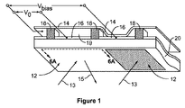
図1は、干渉変調器(IMOD)ディスプレイデバイスの一連のピクセル中の2つの隣接ピクセルを示す等角図の一例を示す。IMODディスプレイデバイスは、1つまたは複数の干渉MEMSディスプレイ要素を含む。これらのデバイスでは、MEMSディスプレイ要素のピクセルが、明状態または暗状態のいずれかにあることがある。明(「緩和」、「開」または「オン」)状態では、ディスプレイ要素は、たとえば、ユーザに、入射可視光の大部分を反射する。逆に、暗(「作動」、「閉」または「オフ」)状態では、ディスプレイ要素は入射可視光をほとんど反射しない。幾つかの実施態様では、オン状態の光反射特性とオフ状態の光反射特性は逆にされ得る。MEMSピクセルは、黒および白に加えて、主に、カラーディスプレイを可能にする特定の波長において、反射するように構成され得る。 FIG. 1 shows an example of an isometric view showing two adjacent pixels in a series of pixels of an interferometric modulator (IMOD) display device. The IMOD display device includes one or more interfering MEMS display elements. In these devices, the pixels of the MEMS display element may be in either a bright state or a dark state. In the bright (“relaxed”, “open” or “on”) state, the display element reflects a large portion of incident visible light, for example, to a user. Conversely, in the dark (“actuated”, “closed” or “off”) state, the display element reflects little incident visible light. In some embodiments, the on-state light reflection characteristics and the off-state light reflection characteristics may be reversed. In addition to black and white, MEMS pixels can be configured to reflect primarily at specific wavelengths that allow for a color display.
IMODディスプレイデバイスは、IMODの行/列アレイを含むことができる。各IMODは、(光ギャップまたはキャビティとも呼ばれる)エアギャップを形成するように互いから可変で制御可能な距離をおいて配置された反射層のペア、すなわち、可動反射層と固定部分反射層とを含むことができる。可動反射層は、少なくとも2つの位置の間で移動され得る。第1の位置、すなわち、緩和位置では、可動反射層は、固定部分反射層から比較的大きい距離をおいて配置され得る。第2の位置、すなわち、作動位置では、可動反射層は、部分反射層により近接して配置され得る。それら2つの層から反射する入射光は、可動反射層の位置に応じて、強め合うようにまたは弱め合うように干渉し、各ピクセルについて全反射状態または無反射状態のいずれかを引き起こすことがある。幾つかの実施態様では、IMODは、作動していないときに反射状態にあり、可視スペクトル内の光を反射し得、また、作動していないときに暗状態にあり、可視範囲外の光(たとえば、赤外光)を反射し得る。ただし、幾つかの他の実施態様では、IMODは、作動していないときに暗状態にあり、作動しているときに反射状態にあり得る。幾つかの実施態様では、印加電圧の導入が、状態を変更するようにピクセルを駆動することができる。幾つかの他の実施態様では、印加電荷が、状態を変更するようにピクセルを駆動することができる。 The IMOD display device can include a row / column array of IMODs. Each IMOD consists of a pair of reflective layers arranged at variable and controllable distances from each other to form an air gap (also called an optical gap or cavity), ie a movable reflective layer and a fixed partially reflective layer. Can be included. The movable reflective layer can be moved between at least two positions. In the first position, i.e. the relaxed position, the movable reflective layer can be arranged at a relatively large distance from the fixed partially reflective layer. In the second position, i.e. the operating position, the movable reflective layer can be placed closer to the partially reflective layer. Incident light that reflects from these two layers interferes constructively or destructively depending on the position of the movable reflective layer, and can cause either total reflection or no reflection for each pixel. . In some embodiments, the IMOD is in a reflective state when not activated, can reflect light in the visible spectrum, and is in a dark state when not activated, with light outside the visible range ( For example, infrared light) can be reflected. However, in some other implementations, the IMOD may be in a dark state when not activated and in a reflective state when activated. In some implementations, introduction of an applied voltage can drive the pixel to change state. In some other implementations, the applied charge can drive the pixel to change state.
図1中のピクセルアレイの図示の部分は、2つの隣接する干渉変調器12を含む。(図示のような)左側のIMOD12では、可動反射層14が、部分反射層を含む光学スタック16からの所定の距離における緩和位置に示されている。左側のIMOD12の両端間に印加された電圧V0は、可動反射層14の作動を引き起こすには不十分である。右側のIMOD12では、可動反射層14は、光学スタック16の近くの、またはそれに隣接する作動位置に示されている。右側のIMOD12の両端間に印加された電圧Vbiasは、可動反射層14を作動位置に維持するのに十分である。
The depicted portion of the pixel array in FIG. 1 includes two
図1では、ピクセル12の反射特性が、概して、ピクセル12に入射する光を示す矢印13と、左側のIMOD12から反射する光15とを用いて示されている。詳細に示していないが、ピクセル12に入射する光13の大部分は透明基板20を透過され、光学スタック16に向かうことになることを、当業者なら理解されよう。光学スタック16に入射する光の一部分は光学スタック16の部分反射層を透過されることになり、一部分は反射され、透明基板20を通って戻ることになる。光学スタック16を透過された光13の部分は、可動反射層14において反射され、透明基板20に向かって(およびそれを通って)戻ることになる。光学スタック16の部分反射層から反射された光と可動反射層14から反射された光との間の(強め合うまたは弱め合う)干渉が、IMOD12から反射される光15の(1つまたは複数の)波長を決定することになる。
In FIG. 1, the reflective characteristics of the
光学スタック16は、単一の層または幾つかの層を含むことができる。その(1つまたは複数の)層は、電極層と、部分反射および部分透過層と、透明な誘電体層とのうちの1つまたは複数を含むことができる。幾つかの実施態様では、光学スタック16は、電気伝導性であり、部分的に透明で、部分的に反射性であり、たとえば、透明基板20上に上記の層のうちの1つまたは複数を堆積させることによって、作製され得る。電極層は、様々な金属、たとえば酸化インジウムスズ(ITO)など、様々な材料から形成され得る。部分反射層は、様々な金属、たとえば、クロム(Cr)、半導体、および誘電体など、部分的に反射性である様々な材料から形成され得る。部分反射層は、材料の1つまたは複数の層から形成され得、それらの層の各々は、単一の材料または材料の組合せから形成され得る。幾つかの実施態様では、光学スタック16は、光吸収体と導体の両方として働く、金属または半導体の単一の半透明の膜(thickness)を含むことができるが、(たとえば、光学スタック16の、またはIMODの他の構造の)異なる、より伝導性の高い層または部分が、IMODピクセル間で信号をバスで運ぶ(bus)ように働くことができる。光学スタック16は、1つまたは複数の伝導性層または伝導性/吸収層をカバーする、1つまたは複数の絶縁層または誘電体層をも含むことができる。
The
幾つかの実施態様では、光学スタック16の(1つまたは複数の)層は、以下でさらに説明するように、平行ストリップにパターニングされ得、ディスプレイデバイスにおける行電極を形成し得る。当業者によって理解されるように、「パターニング」という用語は、本明細書では、マスキングプロセスならびにエッチングプロセスを指すために使用される。幾つかの実施態様では、アルミニウム(Al)などの高伝導性および反射性材料が可動反射層14のために使用され得、これらのストリップはディスプレイデバイスにおける列電極を形成し得る。可動反射層14は、(光学スタック16の行電極に直交する)1つまたは複数の堆積された金属層の一連の平行ストリップとして形成されて、ポスト18の上に堆積された列とポスト18間に堆積された介在する犠牲材料とを形成し得る。犠牲材料がエッチング除去されると、画定されたギャップ19または光キャビティが可動反射層14と光学スタック16との間に形成され得る。幾つかの実施態様では、ポスト18間の間隔は約1〜1000μmであり得、ギャップ19は10,000オングストローム(Å)未満であり得る。
In some implementations, the layer (s) of the
幾つかの実施態様では、IMODの各ピクセルは、作動状態にあろうと緩和状態にあろうと、本質的に、固定反射層および可動反射層によって形成されるキャパシタである。電圧が印加されないとき、可動反射層14は、図1中の左側のIMOD12によって示されるように、機械的に緩和した状態にとどまり、可動反射層14と光学スタック16との間のギャップ19がある。しかしながら、電位差、たとえば、電圧が、選択された行および列のうちの少なくとも1つに印加されたとき、対応するピクセルにおける行電極と列電極との交差部に形成されたキャパシタは帯電し、静電力がそれらの電極を引き合わせる。印加された電圧がしきい値を超える場合、可動反射層14は、変形し、光学スタック16の近くにまたはそれに対して移動することができる。光学スタック16内の誘電体層(図示せず)が、図1中の右側の作動IMOD12によって示されるように、短絡を防ぎ、層14と層16との間の分離距離を制御し得る。その挙動は、印加電位差の極性にかかわらず同じである。幾つかの事例ではアレイ中の一連のピクセルが「行」または「列」と呼ばれることがあるが、ある方向を「行」と呼び、別の方向を「列」と呼ぶことは恣意的であることを、当業者は容易に理解されよう。言い換えれば、幾つかの配向では、行は列と見なされ得、列は行であると見なされ得る。さらに、ディスプレイ要素は、直交する行および列に一様に配置されるか(「アレイ」)、または、たとえば、互いに対して一定の位置オフセットを有する、非線形構成で配置され得る(「モザイク」)。「アレイ」および「モザイク」という用語は、いずれかの構成を指し得る。したがって、ディスプレイは、「アレイ」または「モザイク」を含むものとして言及されるが、その要素自体は、いかなる事例においても、互いに直交して配置される必要がなく、または一様な分布で配設される必要がなく、非対称形状および不均等に分布された要素を有する配置を含み得る。
In some embodiments, each pixel of the IMOD is essentially a capacitor formed by a fixed reflective layer and a movable reflective layer, whether in an active state or in a relaxed state. When no voltage is applied, the movable
図2は、3×3干渉変調器ディスプレイを組み込んだ電子デバイスを示すシステムブロック図の一例を示す。電子デバイスは、1つまたは複数のソフトウェアモジュールを実行するように構成され得るプロセッサ21を含む。オペレーティングシステムを実行することに加えて、プロセッサ21は、ウェブブラウザ、電話アプリケーション、電子メールプログラム、または他のソフトウェアアプリケーションを含む、1つまたは複数のソフトウェアアプリケーションを実行するように構成され得る。
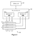
FIG. 2 shows an example of a system block diagram illustrating an electronic device incorporating a 3 × 3 interferometric modulator display. The electronic device includes a
プロセッサ21は、アレイドライバ22と通信するように構成され得る。アレイドライバ22は、たとえば、ディスプレイアレイまたはパネル30に、信号を与える行ドライバ回路24と列ドライバ回路26とを含むことができる。図2には、図1に示したIMODディスプレイデバイスの断面が線1−1によって示されている。図2は明快のためにIMODの3×3アレイを示しているが、ディスプレイアレイ30は、極めて多数のIMODを含んでいることがあり、列におけるIMODの数とは異なる数のIMODを行において有し得、その逆も同様である。
The
図3は、図1の干渉変調器についての可動反射層位置対印加電圧を示す図の一例を示す。MEMS干渉変調器の場合、行/列(すなわち、コモン/セグメント)書込みプロシージャが、図3に示すこれらのデバイスのヒステリシス特性を利用し得る。干渉変調器は、可動反射層またはミラーに緩和状態から作動状態に変更させるために、たとえば、約10ボルトの電位差を必要とし得る。電圧がその値から低減されると、電圧が低下して、たとえば、10ボルトより下に戻ったとき、可動反射層はそれの状態を維持するが、電圧が2ボルトより下に低下するまで、可動反射層は完全には緩和しない。したがって、図3に示すように、印加電圧のウィンドウがある電圧の範囲、約3〜7ボルトが存在し、そのウィンドウ内でデバイスは緩和状態または作動状態のいずれかで安定している。これは、本明細書では「ヒステリシスウィンドウ」または「安定性ウィンドウ」と呼ばれる。図3のヒステリシス特性を有するディスプレイアレイ30の場合、行/列書込みプロシージャは、一度に1つまたは複数の行をアドレス指定するように設計され得、その結果、所与の行のアドレス指定中に、作動されるべきアドレス指定された行におけるピクセルは、約10ボルトの電圧差にさらされ、緩和されるべきピクセルは、ほぼ0ボルトの電圧差にさらされる。アドレス指定後に、それらのピクセルは、それらが前のストローブ状態にとどまるような、約5ボルトの定常状態またはバイアス電圧差にさらされる。この例では、アドレス指定された後に、各ピクセルは、約3〜7ボルトの「安定性ウィンドウ」内の電位差を経験する。このヒステリシス特性の特徴は、たとえば、図1に示した、ピクセル設計が、同じ印加電圧条件下で作動または緩和のいずれかの既存の状態で安定したままであることを可能にする。各IMODピクセルは、作動状態にあろうと緩和状態にあろうと、本質的に、固定反射層および可動反射層によって形成されるキャパシタであるので、この安定状態は、電力を実質的に消費するかまたは失うことなしに、ヒステリシスウィンドウ内の定常電圧において保持され得る。その上、印加電圧電位が実質的に固定のままである場合、電流は本質的にほとんどまたはまったくIMODピクセルに流れ込まない。
FIG. 3 shows an example of a diagram illustrating movable reflective layer position versus applied voltage for the interferometric modulator of FIG. In the case of a MEMS interferometric modulator, a row / column (ie, common / segment) write procedure may take advantage of the hysteresis characteristics of these devices shown in FIG. An interferometric modulator may require, for example, a potential difference of about 10 volts to cause the movable reflective layer or mirror to change from a relaxed state to an activated state. When the voltage is reduced from that value, the voltage drops, for example, when it returns below 10 volts, the movable reflective layer maintains its state, but until the voltage drops below 2 volts, The movable reflective layer does not relax completely. Thus, as shown in FIG. 3, there is a range of voltages, approximately 3-7 volts, where the applied voltage window is within which the device is stable in either a relaxed state or an operating state. This is referred to herein as a “hysteresis window” or “stability window”. For the
幾つかの実施態様では、所与の行におけるピクセルの状態の所望の変化(もしあれば)に従って、列電極のセットに沿って「セグメント」電圧の形態のデータ信号を印加することによって、画像のフレームが作成され得る。次に、フレームが一度に1行書き込まれるように、アレイの各行がアドレス指定され得る。第1の行におけるピクセルに所望のデータを書き込むために、第1の行におけるピクセルの所望の状態に対応するセグメント電圧が列電極上に印加され得、特定の「コモン」電圧または信号の形態の第1の行パルスが第1の行電極に印加され得る。次いで、セグメント電圧のセットは、第2の行におけるピクセルの状態の所望の変化(もしあれば)に対応するように変更され得、第2のコモン電圧が第2の行電極に印加され得る。幾つかの実施態様では、第1の行におけるピクセルは、列電極に沿って印加されたセグメント電圧の変化による影響を受けず、第1のコモン電圧行パルス中にそれらのピクセルが設定された状態にとどまる。このプロセスは、画像フレームを生成するために、一連の行全体、または代替的に、一連の列全体について、連続方式で繰り返され得る。フレームは、何らかの所望の数のフレーム毎秒でこのプロセスを断続的に反復することによって、新しい画像データでリフレッシュおよび/または更新され得る。 In some embodiments, by applying a data signal in the form of a “segment” voltage along a set of column electrodes according to a desired change (if any) in the state of pixels in a given row, A frame can be created. Each row of the array can then be addressed so that the frame is written one row at a time. In order to write the desired data to the pixels in the first row, a segment voltage corresponding to the desired state of the pixels in the first row can be applied on the column electrodes, in the form of a particular “common” voltage or signal. A first row pulse may be applied to the first row electrode. The set of segment voltages can then be changed to correspond to the desired change (if any) in the state of the pixels in the second row, and a second common voltage can be applied to the second row electrode. In some implementations, the pixels in the first row are unaffected by changes in the segment voltage applied along the column electrodes, and the pixels are set during the first common voltage row pulse. Stay on. This process may be repeated in a continuous fashion for the entire series of rows, or alternatively, the entire series of columns, to generate an image frame. The frames can be refreshed and / or updated with new image data by intermittently repeating this process at any desired number of frames per second.
各ピクセルの両端間に印加されるセグメント信号とコモン信号の組合せ(すなわち、各ピクセルの両端間の電位差)は、各ピクセルの得られる状態を決定する。図4は、様々なコモン電圧およびセグメント電圧が印加されたときの干渉変調器の様々な状態を示す表の一例を示している。当業者によって容易に理解されるように、「セグメント」電圧は、列電極または行電極のいずれかに印加され得、「コモン」電圧は、列電極または行電極のうちの他方に印加され得る。 The combination of the segment and common signals applied across each pixel (ie, the potential difference across each pixel) determines the resulting state of each pixel. FIG. 4 shows an example of a table showing various states of the interferometric modulator when various common voltages and segment voltages are applied. As readily understood by those skilled in the art, a “segment” voltage can be applied to either the column electrode or the row electrode, and a “common” voltage can be applied to the other of the column electrode or the row electrode.
図4に(ならびに図5Bに示すタイミング図に)示すように、開放電圧(release voltage)VCRELがコモンラインに沿って印加されたとき、コモンラインに沿ったすべての干渉変調器要素は、セグメントラインに沿って印加された電圧、すなわち、高いセグメント電圧VSHおよび低いセグメント電圧VSLにかかわらず、代替的に開放または非作動状態と呼ばれる、緩和状態に入れられることになる。特に、開放電圧VCRELがコモンラインに沿って印加されると、そのピクセルのための対応するセグメントラインに沿って高いセグメント電圧VSHが印加されたときも、低いセグメント電圧VSLが印加されたときも、変調器の両端間の潜在的な電圧(代替的にピクセル電圧と呼ばれる)は緩和ウィンドウ(図3参照。開放ウィンドウとも呼ばれる)内にある。 As shown in FIG. 4 (as well as in the timing diagram shown in FIG. 5B), all interferometric modulator elements along the common line are segmented when a release voltage VC REL is applied along the common line. voltage applied along the line, i.e., regardless of the high segment voltage VS H and lower segment voltage VS L, is alternatively referred to as open or inoperative state, it will be taken into a relaxed state. In particular, the open circuit voltage VC REL is applied along a common line, even when the corresponding higher along the segment lines to segment voltage VS H for that pixel is applied, a low segment voltage VS L is applied Sometimes, the potential voltage across the modulator (alternatively called the pixel voltage) is within the relaxation window (see FIG. 3, also called the open window).
高い保持電圧VCHOLD_Hまたは低い保持電圧VCHOLD_Lなどの保持電圧がコモンライン上に印加されたとき、干渉変調器の状態は一定のままであることになる。たとえば、緩和IMODは緩和位置にとどまることになり、作動IMODは作動位置にとどまることになる。保持電圧は、対応するセグメントラインに沿って高いセグメント電圧VSHが印加されたときも、低いセグメント電圧VSLが印加されたときも、ピクセル電圧が安定性ウィンドウ内にとどまることになるように、選択され得る。したがって、セグメント電圧スイング(voltage swing)、すなわち、高いVSHと低いセグメント電圧VSLとの間の差は、正または負のいずれかの安定性ウィンドウの幅よりも小さい。 When a holding voltage such as a high holding voltage VC HOLD_H or a low holding voltage VC HOLD_L is applied on the common line, the state of the interferometric modulator will remain constant. For example, the relaxed IMOD will remain in the relaxed position and the activated IMOD will remain in the activated position. Holding voltage, as is when the high segment voltage VS H along the corresponding segment line is applied, even when the lower segment voltage VS L is applied, so that the pixel voltage remains within stability window, Can be selected. Therefore, the segment voltage swing (Voltage swing), i.e., the difference between high VS H and lower segment voltage VS L is smaller than the positive or negative of the width of any of the stability window.
高いアドレス指定電圧VCADD_Hまたは低いアドレス指定電圧VCADD_Lなどのアドレス指定または作動電圧がコモンライン上に印加されたとき、それぞれのセグメントラインに沿ったセグメント電圧の印加によって、データがそのコモンラインに沿った変調器に選択的に書き込まれ得る。セグメント電圧は、作動が印加されたセグメント電圧に依存するように選択され得る。アドレス指定電圧がコモンラインに沿って印加されたとき、一方のセグメント電圧の印加は、安定性ウィンドウ内のピクセル電圧をもたらし、ピクセルが非作動のままであることを引き起こすことになる。対照的に、他方のセグメント電圧の印加は、安定性ウィンドウを越えるピクセル電圧をもたらし、ピクセルの作動をもたらすことになる。作動を引き起こす特定のセグメント電圧は、どのアドレス指定電圧が使用されるかに応じて変動することができる。幾つかの実施態様では、高いアドレス指定電圧VCADD_Hがコモンラインに沿って印加されたとき、高いセグメント電圧VSHの印加は、変調器がそれの現在位置にとどまることを引き起こすことがあり、低いセグメント電圧VSLの印加は、変調器の作動を引き起こすことがある。当然の結果として、低いアドレス指定電圧VCADD_Lが印加されたとき、セグメント電圧の影響は反対であり、高いセグメント電圧VSHは変調器の作動を引き起こし、低いセグメント電圧VSLは変調器の状態に影響しない(すなわち、安定したままである)ことがある。 When an addressing or actuation voltage such as a high addressing voltage VC ADD_H or a low addressing voltage VC ADD_L is applied on a common line, the application of segment voltages along each segment line causes the data to move along that common line. Can be selectively written to the modulator. The segment voltage may be selected such that operation depends on the applied segment voltage. When an addressing voltage is applied along the common line, the application of one segment voltage will result in a pixel voltage within the stability window, causing the pixel to remain inactive. In contrast, application of the other segment voltage results in a pixel voltage that exceeds the stability window, resulting in pixel operation. The particular segment voltage that causes actuation can vary depending on which addressing voltage is used. In some embodiments, when the high addressability voltage VC ADD_H is applied along the common line, application of the high segment voltage VS H, it is possible to cause the modulator remains in the current position of it, low Application of the segment voltage VS L may cause the modulator to operate. As a corollary, when the lower address voltage VC ADD_L is applied, the influence of the segment voltage is the opposite, high segment voltage VS H causes actuation of the modulator, a lower segment voltage VS L in the state of the modulator It may not affect (ie remain stable).
幾つかの実施態様では、常に変調器の両端間で同じ極性電位差を引き起こす保持電圧、アドレス電圧、およびセグメント電圧が使用され得る。幾つかの他の実施態様では、変調器の電位差の極性を交番する信号が使用され得る。変調器の両端間の極性の交番(すなわち、書込みプロシージャの極性の交番)は、単一の極性の反復書込み動作後に起こることがある電荷蓄積を低減または抑止し得る。 In some implementations, a holding voltage, an address voltage, and a segment voltage that always cause the same polarity potential difference across the modulator may be used. In some other implementations, a signal that alternates the polarity of the potential difference of the modulator may be used. The polarity alternation between the ends of the modulator (ie, the polarity alternation of the write procedure) may reduce or inhibit charge accumulation that may occur after a single polarity repetitive write operation.
図5Aは、図2の3×3干渉変調器ディスプレイにおけるディスプレイデータのフレームを示す図の一例を示す。図5Bは、図5Aに示すディスプレイデータのフレームを書き込むために使用され得るコモン信号およびセグメント信号についてのタイミング図の一例を示す。それらの信号は、たとえば、図2の3×3アレイに印加され得、これは、図5Aに示すライン時間60eディスプレイ配置を最終的にもたらすことになる。図5A中の作動変調器は暗状態にあり、すなわち、その状態では、反射光の実質的部分が、たとえば、閲覧者に、暗いアピアランスをもたらすように可視スペクトルの外にある。図5Aに示すフレームを書き込むより前に、ピクセルは任意の状態にあることがあるが、図5Bのタイミング図に示す書込みプロシージャは、各変調器が、第1のライン時間60aの前に、開放されており、非作動状態に属すると仮定する。
FIG. 5A shows an example of a diagram illustrating a frame of display data in the 3 × 3 interferometric modulator display of FIG. FIG. 5B shows an example of a timing diagram for common and segment signals that may be used to write the frame of display data shown in FIG. 5A. Those signals may be applied, for example, to the 3 × 3 array of FIG. 2, which will ultimately result in the line time 60e display arrangement shown in FIG. 5A. The actuating modulator in FIG. 5A is in the dark state, i.e., in that state, a substantial portion of the reflected light is outside the visible spectrum to provide, for example, a dark appearance to the viewer. Prior to writing the frame shown in FIG. 5A, the pixels may be in any state, but the write procedure shown in the timing diagram of FIG. 5B will cause each modulator to open before the
第1のライン時間60a中に、開放電圧70がコモンライン1上に印加され、コモンライン2上に印加される電圧が、高い保持電圧72において始まり、開放電圧70に移動し、低い保持電圧76がコモンライン3に沿って印加される。したがって、コモンライン1に沿った変調器(コモン1,セグメント1)、(1,2)および(1,3)は、第1のライン時間60aの持続時間の間、緩和または非作動状態にとどまり、コモンライン2に沿った変調器(2,1)、(2,2)および(2,3)は、緩和状態に移動することになり、コモンライン3に沿った変調器(3,1)、(3,2)および(3,3)は、それらの前の状態にとどまることになる。図4を参照すると、コモンライン1、2または3のいずれも、ライン時間60a中に作動を引き起こす電圧レベルにさらされていないので(すなわち、VCREL−緩和、およびVCHOLD_L−安定)、セグメントライン1、2および3に沿って印加されたセグメント電圧は、干渉変調器の状態に影響しないことになる。
During the
第2のライン時間60b中に、コモンライン1上の電圧は高い保持電圧72に移動し、コモンライン1に沿ったすべての変調器は、アドレス指定または作動電圧がコモンライン1上に印加されなかったので、印加されたセグメント電圧にかかわらず、緩和状態にとどまる。コモンライン2に沿った変調器は、開放電圧70の印加により、緩和状態にとどまり、コモンライン3に沿った変調器(3,1)、(3,2)および(3,3)は、コモンライン3に沿った電圧が開放電圧70に移動するとき、緩和することになる。
During the
第3のライン時間60c中に、コモンライン1は、コモンライン1上に高いアドレス電圧74を印加することによってアドレス指定される。このアドレス電圧の印加中に低いセグメント電圧64がセグメントライン1および2に沿って印加されるので、変調器(1,1)および(1,2)の両端間のピクセル電圧は変調器の正の安定性ウィンドウの上端よりも大きく(すなわち、電圧差は、あらかじめ定義されたしきい値を超えた)、変調器(1,1)および(1,2)は作動される。逆に、高いセグメント電圧62がセグメントライン3に沿って印加されるので、変調器(1,3)の両端間のピクセル電圧は、変調器(1,1)および(1,2)のピクセル電圧よりも小さく、変調器の正の安定性ウィンドウ内にとどまり、したがって変調器(1,3)は緩和したままである。また、ライン時間60c中に、コモンライン2に沿った電圧は低い保持電圧76に減少し、コモンライン3に沿った電圧は開放電圧70にとどまり、コモンライン2および3に沿った変調器を緩和位置のままにする。
During the third line time 60c, the
第4のライン時間60d中に、コモンライン1上の電圧は、高い保持電圧72に戻り、コモンライン1に沿った変調器を、それらのそれぞれのアドレス指定された状態のままにする。コモンライン2上の電圧は低いアドレス電圧78に減少される。高いセグメント電圧62がセグメントライン2に沿って印加されるので、変調器(2,2)の両端間のピクセル電圧は、変調器の負の安定性ウィンドウの下側端部(lower end)を下回り、変調器(2,2)が作動することを引き起こす。逆に、低いセグメント電圧64がセグメントライン1および3に沿って印加されるので、変調器(2,1)および(2,3)は緩和位置にとどまる。コモンライン3上の電圧は、高い保持電圧72に増加し、コモンライン3に沿った変調器を緩和状態のままにする。
During the
最後に、第5のライン時間60e中に、コモンライン1上の電圧は高い保持電圧72にとどまり、コモンライン2上の電圧は低い保持電圧76にとどまり、コモンライン1および2に沿った変調器を、それらのそれぞれのアドレス指定された状態のままにする。コモンライン3上の電圧は、コモンライン3に沿った変調器をアドレス指定するために、高いアドレス電圧74に増加する。低いセグメント電圧64がセグメントライン2および3上に印加されるので、変調器(3,2)および(3,3)は作動するが、セグメントライン1に沿って印加された高いセグメント電圧62は、変調器(3,1)が緩和位置にとどまることを引き起こす。したがって、第5のライン時間60eの終わりに、3×3ピクセルアレイは、図5Aに示す状態にあり、他のコモンライン(図示せず)に沿った変調器がアドレス指定されているときに起こり得るセグメント電圧の変動にかかわらず、保持電圧がコモンラインに沿って印加される限り、その状態にとどまることになる。
Finally, during the fifth line time 60e, the voltage on
図5Bのタイミング図では、所与の書込みプロシージャ(すなわち、ライン時間60a〜60e)は、高い保持およびアドレス電圧、または低い保持およびアドレス電圧のいずれかの使用を含むことができる。書込みプロシージャが所与のコモンラインについて完了されると(また、コモン電圧が、作動電圧と同じ極性を有する保持電圧に設定されると)、ピクセル電圧は、所与の安定性ウィンドウ内にとどまり、開放電圧がそのコモンライン上に印加されるまで、緩和ウィンドウを通過しない。さらに、各変調器が、変調器をアドレス指定するより前に書込みプロシージャの一部として開放されるので、開放時間ではなく変調器の作動時間が、必要なライン時間を決定し得る。詳細には、変調器の開放時間が作動時間よりも大きい実施態様では、開放電圧は、図5Bに示すように、単一のライン時間よりも長く印加され得る。幾つかの他の実施態様では、コモンラインまたはセグメントラインに沿って印加される電圧が、異なる色の変調器など、異なる変調器の作動電圧および開放電圧の変動を相殺するように変動し得る。
In the timing diagram of FIG. 5B, a given write procedure (ie,
上記に記載した原理に従って動作する干渉変調器の構造の詳細は大きく異なり得る。たとえば、図6A〜図6Eは、可動反射層14とそれの支持構造とを含む、干渉変調器の異なる実施態様の断面図の例を示している。図6Aは、金属材料のストリップ、すなわち、可動反射層14が、基板20から直角に延在する支持体18上に堆積される、図1の干渉変調器ディスプレイの部分断面図の一例を示している。図6Bでは、各IMODの可動反射層14は、概して形状が正方形または長方形であり、コーナーにおいてまたはその近くでテザー32に接して支持体に取り付けられる。図6Cでは、可動反射層14は、概して形状が正方形または長方形であり、フレキシブルな金属を含み得る変形可能層34から吊るされる。変形可能層34は、可動反射層14の外周の周りで基板20に直接または間接的に接続することがある。これらの接続は、本明細書では支持ポストと呼ばれる。図6Cに示す実施態様は、変形可能層34によって行われる可動反射層14の機械的機能からのそれの光学的機能の分離から派生する追加の利益を有する。この分離は、反射層14のために使用される構造設計および材料と、変形可能層34のために使用される構造設計および材料とが、互いとは無関係に最適化されることを可能にする。
The details of the structure of interferometric modulators that operate in accordance with the principles set forth above may vary widely. For example, FIGS. 6A-6E show examples of cross-sectional views of different implementations of interferometric modulators, including a movable
図6Dは、可動反射層14が反射副層(reflective sub−layer)14aを含む、IMODの別の例を示している。可動反射層14は、支持ポスト18などの支持構造上に載る。支持ポスト18は、たとえば、可動反射層14が緩和位置にあるとき、可動反射層14と光学スタック16との間にギャップ19が形成されるように、下側静止電極(すなわち、図示のIMODにおける光学スタック16の一部)からの可動反射層14の分離を可能にする。可動反射層14は、電極として働くように構成され得る伝導性層14cと、支持層14bとをも含むことができる。この例では、伝導性層14cは、基板20から遠位にある支持層14bの一方の面に配設され、反射副層14aは、基板20の近位にある支持層14bの他方の面に配設される。幾つかの実施態様では、反射副層14aは、伝導性であることがあり、支持層14bと光学スタック16との間に配設され得る。支持層14bは、誘電材料、たとえば、酸窒化ケイ素(SiON)または二酸化ケイ素(SiO2)の、1つまたは複数の層を含むことができる。幾つかの実施態様では、支持層14bは、たとえば、SiO2/SiON/SiO23層スタックなど、複数の層のスタックであり得る。反射副層14aと伝導性層14cのいずれかまたは両方は、たとえば、約0.5%の銅(Cu)または別の反射金属材料を用いた、アルミニウム(Al)合金を含むことができる。誘電支持層14bの上および下で伝導性層14a、14cを採用することは、応力のバランスをとり、伝導の向上を与えることができる。幾つかの実施態様では、反射副層14aおよび伝導性層14cは、可動反射層14内の特定の応力プロファイルを達成することなど、様々な設計目的で、異なる材料から形成され得る。
FIG. 6D shows another example of an IMOD in which the movable
図6Dに示すように、幾つかの実施態様はブラックマスク構造23をも含むことができる。ブラックマスク構造23は、周辺光または迷光を吸収するために、光学不活性領域において(たとえば、ピクセル間にまたはポスト18の下に)形成され得る。ブラックマスク構造23はまた、光がディスプレイの不活性部分から反射されることまたはそれを透過されることを抑止し、それによりコントラスト比を増加させることによって、ディスプレイデバイスの光学的特性を改善することができる。さらに、ブラックマスク構造23は、伝導性であり、電気的バス層として機能するように構成され得る。幾つかの実施態様では、行電極は、接続された行電極の抵抗を低減するために、ブラックマスク構造23に接続され得る。ブラックマスク構造23は、堆積およびパターニング技法を含む様々な方法を使用して形成され得る。ブラックマスク構造23は1つまたは複数の層を含むことができる。たとえば、幾つかの実施態様では、ブラックマスク構造23は、光吸収器として働くモリブデンクロム(MoCr)層と、SiO2層と、反射体およびバス層として働く、アルミニウム合金とを含み、それぞれ、約30〜80Å、500〜1000Å、および500〜6000Åの範囲内の厚さである。1つまたは複数の層は、たとえば、MoCr層およびSiO2層の場合は、カーボンテトラフルオロメタン(CF4)および/または酸素(O2)、ならびにアルミニウム合金層の場合は、塩素(Cl2)および/または三塩化ホウ素(BCl3)を含む、フォトリソグラフィおよびドライエッチングを含む、様々な技法を使用してパターニングされ得る。幾つかの実施態様では、ブラックマスク23はエタロンまたは干渉スタック構造であり得る。そのような干渉スタックブラックマスク構造23では、伝導性吸収体は、各行または列の光学スタック16における下側静止電極間で信号を送信するかまたは信号をバスで運ぶために使用され得る。幾つかの実施態様では、スペーサ層35が、ブラックマスク23中の伝導性層から吸収層16aを概して電気的に絶縁するのに、役立つことができる。
Some embodiments may also include a
図6Eは、可動反射層14が自立している、IMODの別の例を示している。図6Dとは対照的に、図6Eの実施態様は支持ポスト18を含まない。代わりに、可動反射層14は、複数のロケーションにおいて、下にある光学スタック16に接触し、可動反射層14の湾曲は、干渉変調器の両端間の電圧が作動を引き起こすには不十分であるとき、可動反射層14が図6Eの非作動位置に戻るという、十分な支持を与える。複数の幾つかの異なる層を含んでいることがある光学スタック16は、ここでは明快のために、光吸収体16aと誘電体16bとを含む状態で示されている。幾つかの実施態様では、光吸収体16aは、固定電極としても、部分反射層としても働き得る。
FIG. 6E shows another example of an IMOD in which the movable
図6A〜図6Eに示す実施態様などの実施態様では、IMODは直視型デバイスとして機能し、直視型デバイスでは、画像が、透明基板20の正面、すなわち、変調器が配置された面の反対の面から、閲覧される。これらの実施態様では、デバイスの背面部分(すなわち、たとえば、図6Cに示す変形可能層34を含む、可動反射層14の背後のディスプレイデバイスの任意の部分)は、反射層14がデバイスのそれらの部分を光学的に遮蔽するので、ディスプレイデバイスの画質に影響を及ぼすことまたは悪影響を及ぼすことなしに、構成され、作用され得る。たとえば、幾つかの実施態様では、バス構造(図示せず)が可動反射層14の背後に含まれ得、これは、電圧アドレス指定およびそのようなアドレス指定に起因する移動など、変調器の電気機械的特性から変調器の光学的特性を分離する能力を与える。さらに、図6A〜図6Eの実施態様は、パターニングなどの処理を簡略化することができる。
In embodiments such as those shown in FIGS. 6A-6E, the IMOD functions as a direct view device where the image is opposite the front of the
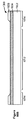
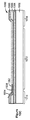
図7は、干渉変調器のための製造プロセス80を示す流れ図の一例を示しており、図8A〜図8Eは、そのような製造プロセス80の対応する段階の断面概略図の例を示している。幾つかの実施態様では、製造プロセス80は、図7に示されていない他のブロックに加えて、たとえば、図1および図6に示す一般的なタイプの干渉変調器を製造するために実施され得る。図1、図6および図7を参照すると、プロセス80はブロック82において開始し、基板20上への光学スタック16の形成を伴う。図8Aは、基板20上で形成されたそのような光学スタック16を示している。基板20は、ガラスまたはプラスチックなどの透明基板であり得、それは、フレキシブルであるかまたは比較的固く曲がらないことがあり、光学スタック16の効率的な形成を可能にするために、事前準備プロセス、たとえば、洗浄にかけられていることがある。上記で説明したように、光学スタック16は、電気伝導性であり、部分的に透明で、部分的に反射性であることがあり、たとえば、透明基板20上に、所望の特性を有する1つまたは複数の層を堆積させることによって、作製され得る。図8Aでは、光学スタック16は、副層16aおよび16bを有する多層構造を含むが、幾つかの他の実施態様では、より多いまたはより少ない副層が含まれ得る。幾つかの実施態様では、副層16a、16bのうちの1つは、組み合わせられた導体/吸収体副層16aなど、光吸収特性と伝導特性の両方で構成され得る。さらに、副層16a、16bのうちの1つまたは複数は、平行ストリップにパターニングされ得、ディスプレイデバイスにおける行電極を形成し得る。そのようなパターニングは、当技術分野で知られているマスキングおよびエッチングプロセスまたは別の好適なプロセスによって実行され得る。幾つかの実施態様では、副層16a、16bのうちの1つは、1つまたは複数の金属層(たとえば、1つまたは複数の反射層および/または伝導性層)上に堆積された副層16bなど、絶縁層または誘電体層であり得る。さらに、光学スタック16は、ディスプレイの行を形成する個々の平行ストリップにパターニングされ得る。
FIG. 7 shows an example of a flow diagram illustrating a
プロセス80はブロック84において続き、光学スタック16上への犠牲層25の形成を伴う。犠牲層25は、キャビティ19を形成するために後で(たとえば、ブロック90において)除去され、したがって、犠牲層25は、図1に示した得られた干渉変調器12には示されていない。図8Bは、光学スタック16上で形成された犠牲層25を含む、部分的に作製されたデバイスを示している。光学スタック16上での犠牲層25の形成は、後続の除去後に、所望の設計サイズを有するギャップまたはキャビティ19(図1および図8Eも参照)を与えるように選択された厚さの、モリブデン(Mo)またはアモルファスシリコン(Si)など、フッ化キセノン(XeF2)エッチング可能材料の堆積を含み得る。犠牲材料の堆積は、物理堆積(PVD、たとえば、スパッタリング)、プラズマ強化化学堆積(PECVD)、熱化学堆積(熱CVD)、またはスピンコーティングなど、堆積技法を使用して行われ得る。
プロセス80はブロック86において続き、支持構造、たとえば、図1、図6および図8Cに示すポスト18の形成を伴う。ポスト18の形成は、支持構造開口を形成するために犠牲層25をパターニングすることと、次いで、PVD、PECVD、熱CVD、またはスピンコーティングなど、堆積方法を使用して、ポスト18を形成するために開口中に材料(たとえば、ポリマーまたは無機材料、たとえば、酸化ケイ素)を堆積させることとを含み得る。幾つかの実施態様では、犠牲層中に形成された支持構造開口は、ポスト18の下側端部が図6Aに示すように基板20に接触するように、犠牲層25と光学スタック16の両方を通って、下にある基板20まで延在することがある。代替的に、図8Cに示すように、犠牲層25中に形成された開口は、犠牲層25は通るが、光学スタック16は通らないで、延在することがある。たとえば、図8Eは、光学スタック16の上側表面(upper surface)と接触している支持ポスト18の下側端部を示している。ポスト18、または他の支持構造は、犠牲層25上に支持構造材料の層を堆積させることと、パターニングして犠牲層25中の開口から離れて配置された支持構造材料の部分を除去することとによって形成され得る。支持構造は、図8Cに示すように開口内に配置され得るが、少なくとも部分的に、犠牲層25の一部分の上で延在することもある。上述のように、犠牲層25および/または支持ポスト18のパターニングは、パターニングおよびエッチングプロセスによって実行され得るが、代替エッチング方法によっても実行され得る。
プロセス80はブロック88において続き、図1、図6および図8Dに示す可動反射層14などの可動反射層または膜の形成を伴う。可動反射層14は、1つまたは複数のパターニング、マスキング、および/またはエッチングプロセスとともに、1つまたは複数の堆積プロセス、たとえば、反射層(たとえば、アルミニウム、アルミニウム合金)堆積を採用することによって、形成され得る。可動反射層14は、電気伝導性であり、電気伝導性層(electrically conductive layer)と呼ばれることがある。幾つかの実施態様では、可動反射層14は、図8Dに示すように複数の副層14a、14b、14cを含み得る。幾つかの実施態様では、副層14a、14cなど、副層のうちの1つまたは複数は、それらの光学的特性のために選択された高反射性副層を含み得、別の副層14bは、それの機械的特性のために選択された機械的副層を含み得る。犠牲層25は、ブロック88において形成された部分的に作製された干渉変調器中に依然として存在するので、可動反射層14は、一般にこの段階では可動でない。犠牲層25を含んでいる部分的に作製されたIMODは、本明細書では「非開放(unreleased)」IMODと呼ばれることもある。図1に関して上記で説明したように、可動反射層14は、ディスプレイの列を形成する個々の平行ストリップにパターニングされ得る。
プロセス80はブロック90において続き、キャビティ、たとえば、図1、図6および図8Eに示すキャビティ19の形成を伴う。キャビティ19は、(ブロック84において堆積された)犠牲材料25をエッチャントにさらすことによって形成され得る。たとえば、MoまたはアモルファスSiなどのエッチング可能犠牲材料が、ドライ化学エッチングによって、たとえば、一般に、キャビティ19を囲む構造に対して選択的に除去される、所望の量の材料を除去するのに有効である期間の間、固体XeF2から派生した蒸気などの気体または蒸気エッチャントに犠牲層25をさらすことによって、除去され得る。エッチング可能な犠牲材料およびエッチング方法、たとえば、ウェットエッチングおよび/またはプラズマエッチングによる他の組合せも使用され得る。犠牲層25がブロック90中に除去されるので、可動反射層14は、一般に、この段階後に可動となる。犠牲材料25の除去後に、得られた完全にまたは部分的に作製されたIMODは、本明細書では「開放」IMODと呼ばれることがある。
基板に関連付けられた様々な半導体および/またはEMSデバイスの垂直集積または相互接続は、デバイスの様々な層間の信号ルーティングに制限を課すことがある。さらに、デバイスの様々な層中の様々な材料の処理に関する課題があり得る。 Vertical integration or interconnection of various semiconductor and / or EMS devices associated with a substrate may impose limitations on signal routing between the various layers of the device. In addition, there can be challenges related to the processing of various materials in various layers of the device.
たとえば、フラットパネルディスプレイなどの装置は、IMODを含むEMSデバイスなど、幾つかのピクセルデバイスを含むピクセルアレイと、マトリックス型能動スイッチおよびドライバ、ならびに蓄積/感知キャパシタおよび抵抗器などの受動デバイスなど、他の構成要素とを含み得る。ピクセルデバイスおよび他の構成要素は、層中に様々な材料をもつ多層構造を含み得る。装置の動作のために、信号は、各ピクセルデバイスの様々な層に、および各ピクセルデバイスの様々な層からルーティングされる必要があり得る。この信号ルーティングを達成するためのビア構造は、十分な充填率を有するために、ほんのわずかのピクセルデバイス面積を占有し得る。ビア構造の作製は、処理を複雑にし得る、ピクセルデバイスの多層構造中の様々な材料を処理することを伴い得る。 For example, devices such as flat panel displays include pixel arrays including several pixel devices, such as EMS devices including IMOD, matrix active switches and drivers, and passive devices such as storage / sense capacitors and resistors, etc. And the components. Pixel devices and other components may include multilayer structures with various materials in the layers. For operation of the device, signals may need to be routed to and from the various layers of each pixel device. The via structure to achieve this signal routing can occupy only a small pixel device area in order to have a sufficient fill factor. The creation of via structures can involve processing various materials in the multilayer structure of the pixel device, which can complicate processing.
代替的に、スタックビア構造のための作製プロセスは、本明細書でさらに説明するように、一度に1つの材料の層をエッチングすることを含み得る。スタックビア構造は、複数の金属層を含み得る。複数の金属層は、スタックビア構造の中心部分において互いに接触し得る。複数の金属層は、スタックビア構造の周辺部分中で、金属層間に配設された誘電体層を有し得る。 Alternatively, the fabrication process for a stacked via structure can include etching one layer of material at a time, as further described herein. The stacked via structure can include multiple metal layers. The plurality of metal layers can contact each other in the central portion of the stacked via structure. The plurality of metal layers may have a dielectric layer disposed between the metal layers in the peripheral portion of the stacked via structure.
図9は、スタックビア構造のための製造プロセスを示す流れ図の一例を示す。図10A〜10Eは、図9に記載されたプロセスの様々な段階におけるスタックビア構造の断面概略図の例を示す。図9は、単一のスタックビア構造を製造するためのプロセスを示すが、複数のスタックビア構造が基板の表面上に同時に製造され得る。加えて、また図示の簡略化のために、図9および図10A〜10Eは、3スタックビア構造のための製造プロセスおよび概略図を示す。3つより多い、またはより少ないスタックビアを有する構造を製作するために、これらのプロセスおよび概略図が繰り返され、かつ/または調整され得ることは、当業者には容易に理解されよう。さらに、スタックビア構造を製造するために使用される、図9に記載されたプロセス動作はまた、スタックビア構造を製造しながら、半導体デバイスまたはEMSデバイスなどのデバイスを作製するためにも使用され得る。 FIG. 9 shows an example of a flow diagram illustrating a manufacturing process for a stacked via structure. 10A-10E show cross-sectional schematic examples of stacked via structures at various stages of the process described in FIG. Although FIG. 9 shows a process for fabricating a single stacked via structure, multiple stacked via structures can be fabricated simultaneously on the surface of the substrate. In addition, and for simplicity of illustration, FIGS. 9 and 10A-10E show a manufacturing process and schematic for a three stack via structure. Those skilled in the art will readily appreciate that these processes and schematics can be repeated and / or adjusted to fabricate structures having more or less than three stacked vias. Further, the process operations described in FIG. 9 used to fabricate a stacked via structure can also be used to fabricate devices such as semiconductor devices or EMS devices while fabricating the stacked via structure. .
最初に図9を参照すると、プロセス900のブロック902において、第1の金属層が基板の表面上に堆積される。基板は、透明な材料、不透明な材料、可撓性材料、剛性材料、またはこれらの組合せを含む、様々な基板材料を含み得る。幾つかの実施態様では、基板は、シリコン、シリコンオンインシュレータ(SOI)、ガラス(ディスプレイガラスもしくはホウケイ酸ガラスなど)、可撓性プラスチック、または金属箔である。幾つかの実施態様では、基板は、数ミクロンから数百ミクロンの寸法を有し得る。幾つかの他の実施態様では、基板は、数十、数百、または数千センチメートルの寸法を有し得る。
Referring initially to FIG. 9, at
基板は、中心部分と周辺部分とを含み得る。これらは、スタックビア構造の中心部分およびスタックビア構造の周辺部分がその上にそれぞれ形成され得る部分である。スタックビア構造の中心部分中で、複数の金属層が互いに接触し得る。スタックビア構造の周辺部分中で、複数の金属層の各々は、それと複数の金属層のうちの別の金属層との間に、誘電体層を有し得る。基板はまた、周辺部分を越えて延在する領域をも含み得る。幾つかの実施態様では、半導体デバイスおよび/もしくはEMSデバイスなどの1つもしくは複数のデバイス、ならびに/または、スタックビア構造から1つもしくは複数のデバイスへの伝導性トレースは、これらの延在する領域の上に形成され得る。スタックビア構造はまた、その周辺部分を越えて延在し得る。周辺部分を越えて延在するスタックビア構造の領域中に、複数の金属層が存在しなくてもよい。複数の金属層のうちの1つまたは複数が、スタックビア構造の周辺部分を越えて延在する領域中に存在するとき、複数の金属層の各々は、それと複数の金属層のうちの別の金属層との間に、誘電体層を有し得る。 The substrate can include a central portion and a peripheral portion. These are portions on which the central portion of the stacked via structure and the peripheral portion of the stacked via structure can be formed, respectively. Multiple metal layers can contact each other in the central portion of the stacked via structure. In the peripheral portion of the stacked via structure, each of the plurality of metal layers may have a dielectric layer between it and another metal layer of the plurality of metal layers. The substrate may also include a region that extends beyond the peripheral portion. In some implementations, the conductive traces from one or more devices, such as semiconductor devices and / or EMS devices, and / or one or more devices from a stacked via structure may extend these extended regions. Can be formed on top of each other. The stacked via structure can also extend beyond its peripheral portion. A plurality of metal layers may not be present in the region of the stacked via structure that extends beyond the peripheral portion. When one or more of the plurality of metal layers are present in a region extending beyond the peripheral portion of the stacked via structure, each of the plurality of metal layers is associated with another of the plurality of metal layers. There may be a dielectric layer between the metal layer.
幾つかの実施態様では、基板の表面はバッファ層を含み得る。バッファ層は、基板の表面を密封するために絶縁表面またはパッシベーション層としての働きをし得る。幾つかの実施態様では、バッファ層は、SiO2、窒化ケイ素(SixN)、SiON、炭化ケイ素(SiC)、酸化チタン(TiO2)、酸化アルミニウム(Al2O3)、またはスピンオンガラス(SOG)など、誘電体であり得る。幾つかの実施態様では、バッファ層は、ポリイミド、ベンゾシクロブテン(BCB、C8H8)、またはフォトレジスト(たとえば、エポキシベースのフォトレジスト)など、ポリマーであり得る。バッファ層はまた、これらの材料の任意の多層組合せであってもよい。幾つかの実施態様では、バッファ層は、約1ミクロンの厚さなど、約100ナノメートル(nm)から10ミクロンの厚さであり得る。 In some implementations, the surface of the substrate can include a buffer layer. The buffer layer can act as an insulating surface or passivation layer to seal the surface of the substrate. In some embodiments, the buffer layer comprises SiO 2 , silicon nitride (Si x N), SiON, silicon carbide (SiC), titanium oxide (TiO 2 ), aluminum oxide (Al 2 O 3 ), or spin-on glass ( SOG) or the like. In some implementations, the buffer layer can be a polymer, such as polyimide, benzocyclobutene (BCB, C 8 H 8 ), or a photoresist (eg, an epoxy-based photoresist). The buffer layer may also be any multilayer combination of these materials. In some implementations, the buffer layer can be about 100 nanometers (nm) to 10 microns thick, such as about 1 micron thick.
第1の金属層は、基板の中心部分および周辺部分上に堆積され得る。第1の金属層は、アルミニウム(Al)、金(Au)、銅(Cu)、モリブデン(Mo)、タンタル(Ta)、クロム(Cr)、ネオジム(Nd)、タングステン(W)、チタン(Ti)、ニッケル(Ni)など、任意の数の異なる金属、ならびに、MoCr、AlCu、およびAlSiなど、これらの金属のうちの少なくとも1つを含む合金を含み得る。幾つかの実施態様では、第1の金属層は、約10nm未満の厚さ、数十ナノメートルの厚さ、数百ナノメートルの厚さ、または数ミクロンの厚さであり得る。第1の金属層は、PVDプロセス、CVDプロセス、または原子層堆積(ALD)プロセスなどの堆積プロセスを使用して堆積され得る。 The first metal layer can be deposited on the central portion and the peripheral portion of the substrate. The first metal layer is made of aluminum (Al), gold (Au), copper (Cu), molybdenum (Mo), tantalum (Ta), chromium (Cr), neodymium (Nd), tungsten (W), titanium (Ti) ), Nickel (Ni), etc., any number of different metals, and alloys containing at least one of these metals, such as MoCr, AlCu, and AlSi. In some embodiments, the first metal layer can be less than about 10 nm thick, tens of nanometers thick, hundreds of nanometers thick, or several microns thick. The first metal layer may be deposited using a deposition process such as a PVD process, a CVD process, or an atomic layer deposition (ALD) process.
ブロック904において、第1の金属層がパターニングされる。リソグラフィプロセスならびに(プラズマエッチング、反応性イオンエッチング(RIE)、イオンビームミリングなどを含む、ウェットエッチングまたはドライエッチングなどの)エッチングプロセスを含む、パターニング技法が、第1の金属層を含む基板の部分を画定するために使用され得る。たとえば、第1の金属層は、形成された後、フォトレジストを用いてパターニングされ得る。次いで、第1の金属層は、第1の金属層の部分を基板の表面の選択された部分から除去するためにエッチングされ得る。第1の金属層は、第1の金属がスタックビア構造の中心部分と、デバイスへの伝導性トレースと、デバイスの構成要素とを形成するように、パターニングされ得る。
At
図10Aは、プロセス900のこの時点(たとえば、ブロック904まで)におけるスタックビア構造の断面概略図の一例を示す。スタックビア構造1000は、基板1002と第1の金属層1004とを含む。基板1002は、中心部分1012と周辺部分1014とを含む。図10A〜10Eは、プロセス900の幾つかの段階におけるスタックビア構造の断面概略図の例を示す。基板1002の周辺部分1014を越えて延在する領域(図示せず)は、基板上に延在し得、伝導性トレース、ならびに/または能動デバイスおよび受動デバイスを含み得る。
FIG. 10A shows an example of a cross-sectional schematic diagram of a stacked via structure at this point in the process 900 (eg, up to block 904). The stacked via
図9に戻ると、ブロック906において、第1の誘電体層が堆積およびパターニングされる。第1の誘電体層の誘電体は、SiO2、SiC、Al2O3、酸化ハフニウム(HfO2)、TiO2、SiON、SixNなど、任意の数の異なる誘電体を含み得る。幾つかの実施態様では、各誘電体層は、約5ミクロン未満の厚さ、または約100nm未満の厚さであり得る。幾つかの実施態様では、各誘電体層は、約数十ナノメートルから1ミクロンの厚さ、または約1ミクロンの厚さであり得る。第1の誘電体層は、PVDプロセス、CVDプロセス、またはALDプロセスなどの堆積プロセスを使用して堆積され得る。第1の誘電体層は、第1の誘電体層がスタックビア構造の中心部分に存在しないが、スタックビア構造の周辺部分に残るように、パターニングされ得る。上記で説明したように、リソグラフィプロセスならびにエッチングプロセスを含む、パターニング技法が使用され得る。
Returning to FIG. 9, at
図10Bは、プロセス900のこの時点(たとえば、ブロック906まで)におけるスタックビア構造1000の断面概略図の一例を示す。スタックビア構造1000は、基板1002と、第1の金属層1004と、第1の誘電体層1006とを含む。第1の誘電体層は、基板1002の中心部分1012の上にないが、基板1002の周辺部分1014の上にある。
FIG. 10B shows an example of a cross-sectional schematic diagram of a stacked via
図9に戻ると、スタックビア構造のための製造プロセス900は、金属の層を堆積させること、金属の層をパターニングすること、誘電体の層を堆積させること、および誘電体の層をパターニングすることを続ける。これらのプロセスは、所望のスタックビア構造が形成されるまで繰り返され得る。たとえば、ブロック908において、第2の金属層が堆積およびパターニングされる。幾つかの実施態様では、第2の金属層は、第1の金属層と同じ金属を含み得、幾つかの実施態様では、第2の金属層は、第1の金属層とは異なる金属を含み得る。幾つかの実施態様では、第2の金属層は、第1の金属層と同じ厚さであり得、幾つかの実施態様では、第2の金属層は、第1の金属層とは異なる厚さであり得る。
Returning to FIG. 9, a
図10Cは、プロセス900のこの時点(たとえば、ブロック908まで)におけるスタックビア構造1000の断面概略図の一例を示す。スタックビア構造1000は、基板1002と、第1の金属層1004と、第1の誘電体層1006と、第2の金属層1008とを含む。第2の金属層1008は、部分的に基板1002の中心部分1012の上にあるエリア中で第1の金属層1004に接触し、周辺部分1014の上にあるエリア中で第1の誘電体層1006に接触する。第2の金属層1008は、第2の金属層1008が傾斜部分1054を含むように、第1の誘電体層1006のエッジと共形である。第2の金属層1008の平面部分1052が傾斜部分1054と作り出す角度1038は、約90度から150度であり得る。幾つかの実施態様では、スタックビア構造を形成する後続の金属層は、同様の傾斜部分を含み得る。金属層の傾斜部分と平面部分との間の角度は、均一であるか、またはスタックビア構造の両端間で変動し得る。たとえば、任意の2つの金属層は、同じまたは異なる角度を含み得る。
FIG. 10C shows an example of a cross-sectional schematic diagram of the stacked via
図9に示すプロセス900のブロック910において、第2の誘電体層が堆積およびパターニングされる。幾つかの実施態様では、第2の誘電体層は、第1の誘電体層と同じ誘電体を含み得、幾つかの実施態様では、第2の誘電体層は、第1の誘電体層とは異なる誘電体を含み得る。幾つかの実施態様では、第2の誘電体層は、第1の誘電体層と同じ厚さであり得、幾つかの実施態様では、第2の誘電体層は、第1の誘電体層とは異なる厚さであり得る。第2の誘電体層は、第2の誘電体層がスタックビア構造の中心部分に存在しないが、スタックビア構造の周辺部分に残るように、パターニングされ得る。
In
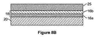
図10Dは、プロセス900のこの時点(たとえば、ブロック910まで)におけるスタックビア構造1000の断面概略図の一例を示す。スタックビア構造1000は、基板1002と、第1の金属層1004と、第1の誘電体層1006と、第2の金属層1008と、第2の誘電体層1010とを含む。第2の誘電体層は、基板1002の中心部分1012の上にないが、基板1002の周辺部分1014の上にある。
FIG. 10D shows an example of a cross-sectional schematic diagram of the stacked via
図9に示すプロセス900のブロック912において、第3の金属層が堆積およびパターニングされる。幾つかの実施態様では、第3の金属層は、第1の金属層と同じ金属を含み得、幾つかの実施態様では、第3の金属層は、第1の金属層とは異なる金属を含み得る。幾つかの実施態様では、第3の金属層は、第1の金属層と同じ厚さであり得、幾つかの実施態様では、第3の金属層は、第1の金属層とは異なる厚さであり得る。
At
図10Eは、プロセス900のこの時点(たとえば、ブロック912まで)におけるスタックビア構造1000の断面概略図の一例を示す。スタックビア構造1000は、基板1002と、第1の金属層1004と、第1の誘電体層1006と、第2の金属層1008と、第2の誘電体層1010と、第3の金属層1013とを含む。第3の金属層1013は、基板1002の中心部分1012の上にあるエリア中で第2の金属層1008に接触する。したがって、幾つかの実施態様では、第1の金属層1004、第2の金属層1008、および第3の金属層1013は、中心部分1012の上にあるエリア中で互いに電気接触し得る。基板の周辺部分1014の上にあるスタックビア構造の部分中で、誘電体層が金属層間に存在し得る。図10Eの例では、第1の誘電体層1006は、周辺部分1014の上にあるエリア中で、第1の金属層1004および第2の金属層1008を分離する。同様に、第2の誘電体層1010は、周辺部分1014の上にあるエリア中で、第2の金属層1008および第3の金属層1013を分離する。したがって、幾つかの実施態様では、第1の金属層1004、第2の金属層1008、および第3の金属層1013は、基板1002の周辺部分1014の上にあるエリア中で互いから電気的に絶縁され得る。
FIG. 10E shows an example of a cross-sectional schematic diagram of the stacked via
スタックビア構造の形成のためのプロセス900では、一度に1つのタイプの材料がパターニングされている。たとえば、ブロック904において、第1の金属層がパターニングされ、このパターニングは、第1の金属層をエッチングすることを含み得る。ブロック906において、第1の誘電体層がパターニングされ、このパターニングは、第1の誘電体層をエッチングすることを含み得る。プロセス900におけるブロック908、910、および912は、一度に1つの層がパターニングされる点で同様である。幾つかの実施態様では、一度に単一の層をパターニングすることは、その層をエッチングすることを含み得る。一度に単一の材料をエッチングすることは、スタックビア構造の作製プロセスを助け得る。たとえば、スタックビア構造のための製造プロセスにおいて様々な材料がエッチングされる場合、異なる速度で異なる材料をエッチングするエッチャントのために、またはエッチング停止層の使用のために、プロセスがより複雑になり得る。
In a
さらに、プロセス900は、3つの金属層と2つの誘電体層とを含む、図10Eに示すスタックビア構造1000を生じ得るが、プロセス900は、金属層および誘電体層の堆積およびパターニングを続け得る。たとえば、スタックビア構造は、任意の数の金属層と、スタックビア構造の周辺部分中で金属層を分離する誘電体層とを含み得る。たとえば、スタックビア構造は、2から12個の金属層を含み得、幾つかの実施態様では、設計構成に応じて、12個以上の層を含み得る。
Further,
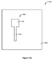
図11A〜11Fは、製造プロセスの様々な段階における2つのスタックビア構造のトップダウン図の例を示す。例示のために、スタックビア構造の周辺部分は、図11A〜11Fに示されていない。たとえば、図11Aは、図9に示すプロセス900のブロック902および904後に形成された装置の一例であり得る。図11Aに示す装置1100は、第1の金属層1004が堆積およびパターニングされた基板1002を含む。第1の金属層1004は、第1のスタックビア構造の中心部分1102と、中心部分1102に結合された伝導性トレース1104とを含むようにパターニングされる。伝導性トレース1104は、第1のスタックビア構造の周辺部分を越えて延在する領域にあり得る。伝導性トレースの端部は、基板1002の表面上で第1のデバイス(図示せず)に結合され得、または第1のデバイス(図示せず)の一部を形成し得る。
11A-11F show examples of top-down views of two stacked via structures at various stages of the manufacturing process. For illustration purposes, the peripheral portion of the stacked via structure is not shown in FIGS. For example, FIG. 11A may be an example of an apparatus formed after
図11Aでは、第1のスタックビア構造の中心部分1102は、実質的に正方形を有するように示される。第1のスタックビア構造の正方形の中心部分1102の一辺は、幾つかの実施態様では、約0.1ミクロンから1ミクロン、約1ミクロンから5ミクロン、約15ミクロンから45ミクロン、または約10ミクロンから100ミクロンの寸法を有し得る。第1のスタックビア構造の中心部分1102はまた、幾つかの実施態様では、長方形、円形、または楕円形を含む、他の形状をも有し得る。そのような第1のスタックビア構造の中心部分の寸法もまた、幾つかの実施態様では、約0.1ミクロンから1ミクロン、約1ミクロンから5ミクロン、約15ミクロンから45ミクロン、または約10ミクロンから100ミクロンであり得る。
In FIG. 11A, the
図11Bは、第1の誘電体層1006が堆積およびパターニングされた後の装置1100を示す。たとえば、図11Bは、図9に示すプロセス900のブロック906後に形成された装置の一例であり得る。誘電体層1006は、伝導性トレース1104を覆う。誘電体層1006は、第1のスタックビア構造の中心部分1102を露出するようにパターニングされる。幾つかの実施態様では、第1の誘電体層1006は、EMSデバイス、トランジスタ、またはキャパシタの一部であり得る。たとえば、誘電体層1006は、トランジスタのためのゲート誘電体、キャパシタのための絶縁体、またはEMSデバイスのための様々な機能的構造のうちの1つとして形成され得る。
FIG. 11B shows the
図11Cは、第2の金属層1108が堆積およびパターニングされた後の装置1100を示す。たとえば、図11Cは、図9に示すプロセス900のブロック908後に形成された装置の一例であり得る。第2の金属層1008は、第1のスタックビア構造の中心部分1122を含むようにパターニングされる。第2の金属層はまた、第2のスタックビア構造の中心部分1112と、中心部分1112に結合された伝導性トレース1114とを含むようにパターニングされる。伝導性トレース1114は、第2のスタックビア構造の周辺部分を越えて延在する領域にあり得る。伝導性トレースの端部は、基板1002の表面上で第1のデバイス(図示せず)に結合され得、または第1のデバイス(図示せず)の一部を形成し得る。
FIG. 11C shows the
図11Dは、第2の誘電体層1010が堆積およびパターニングされた後の装置1100を示す。たとえば、図11Dは、図9に示すプロセス900のブロック910後に形成された装置の一例であり得る。第2の誘電体層1010は、伝導性トレース1114を覆う。第2の誘電体層1010は、第1のスタックビア構造の中心部分1122と第2のスタックビア構造の中心部分1112とを露出するようにパターニングされ得る。上記で説明した第1の誘電体層1006と同様に、第2の誘電体層1010もまた、EMSデバイス、トランジスタ、またはキャパシタの一部であり得る。たとえば、第2の誘電体層1010は、トランジスタのためのゲート誘電体、キャパシタのための絶縁体、またはEMSデバイスのための様々な機能的構造のうちの1つとして形成され得る。
FIG. 11D shows the
図11Eは、第3の金属層1013が堆積およびパターニングされた後の装置1100を示す。たとえば、図11Eは、図9に示すプロセス900のブロック912後に形成された装置の一例であり得る。第3の金属層1013は、第2のスタックビア構造の中心部分1132を含むようにパターニングされる。第3の金属層1013はまた、第1のスタックビア構造の中心部分1142と、その中心部分に結合された伝導性トレース1124とを含むようにパターニングされ得る。伝導性トレース1124は、第1のスタックビア構造の周辺部分を越えて延在する領域にあり得る。伝導性トレースの端部は、たとえば、基板の表面上に作製されることになる第2のデバイス(図示せず)に結合され得、または基板902の表面上に作製されることになる第2のデバイス(図示せず)の一部を形成し得る。代替的に、伝導性トレースの端部は、別の基板上の別のデバイスまたはシステム(図示せず)への相互接続を与え得る。第2のスタックビア構造の中心部分1132中に含まれる第3の金属層1013は、第1のデバイス(図示せず)への相互接続を与え得る。
FIG. 11E shows the
図11Fは、装置1100のトップダウン図を示す。例示のために、図11Fは、互いからオフセットされている金属層を示し、誘電体層を除く。装置1100は、基板1002の表面上に第1の金属層1004が堆積およびパターニングされた、基板1002を含む。第1の金属層1004は、第1のスタックビア構造の中心部分1102と、中心部分1102に結合された伝導性トレース1104とを含む。堆積およびパターニングされる第2の金属層1008は、第1のスタックビア構造の中心部分1122を含む。第2の金属層1008はまた、第2のスタックビア構造の中心部分1112と、中心部分1112に結合された伝導性トレース1114とを含む。堆積およびパターニングされる第3の金属層1013は、第2のスタックビア構造の中心部分1132を含む。第3の金属層1013はまた、第1のスタックビア構造の中心部分1142と、中心部分1142に結合された伝導性トレース1124とを含む。
FIG. 11F shows a top-down view of
図12は、スタックビア構造の投影断面概略図の一例を示す。図12は、図11A〜11Fに示す装置1100の投影断面概略図の一例を示す。上記で説明したように、装置1100は、基板1002と、第1の金属層1004と、第1の誘電体層1006と、第2の金属層1008と、第2の誘電体層1010と、第3の金属層1013とを含む。金属層および誘電体層のうちの一部は、第1のスタックビア構造1202、第2のスタックビア構造1204、および第1のデバイス1206中に含まれる。第1の金属層1004は、第1のスタックビア構造1202の一部、ならびに第1のデバイス1206への伝導性トレースを形成する。金属層1004、1008、および1013は、第1のスタックビア構造1202の中心部分において互いに電気接触し得る。
FIG. 12 shows an example of a schematic sectional view of a stacked via structure. FIG. 12 shows an example of a schematic cross sectional view of the
第2の金属層1008は、第2のスタックビア構造1204の一部、ならびに第1のデバイス1206への伝導性トレースを形成する。金属層1008および1013は、第2のスタックビア構造1204の中心部分において互いに電気接触し得る。
The
図12に示すように、第1の金属層1004および/または第2の金属層1008は、第1のデバイス1206の一部を形成し得る。たとえば、第1の金属層1004および/または第2の金属層1008は、薄膜トランジスタデバイスのゲート電極、蓄積キャパシタデバイスの電極、抵抗器デバイスの構成要素、または、EMSデバイスもしくはEMSディスプレイデバイスのヒンジ構造、ミラースタック、複合膜、カンチレバー、もしくは梁の一部を形成し得る。幾つかの実施態様では、第1の誘電体層1006および/または第2の誘電体層1010もまた、第1のデバイス1206中に含まれ得る。たとえば、第1の誘電体層1106および/または第2の誘電体層1110は、薄膜トランジスタデバイスのゲート誘電体、蓄積キャパシタデバイスの誘電体層、EMSディスプレイデバイスの可動層のためのポスト構造、または、EMSデバイスのカンチレバー、梁、もしくは複合膜を形成し得る。
As shown in FIG. 12, the
幾つかの実施態様では、第1の金属層1004および第2の金属層1008は、第1のデバイス1206の一部を形成することなしに、第1のデバイス1206への伝導性トレースを含み得る。
In some implementations, the
さらに、図12に示すように、スタックビア構造1202および1204は、(たとえば、第2のスタックビア構造1204を使用して)装置1100の上部から、または(たとえば、第1のビア構造1202に結合されたトレースを用いて)装置1100の側部からの、デバイス1206への接続を可能にする。
Further, as shown in FIG. 12, stacked via
本明細書で説明したように、スタックビア構造を形成することは、堆積プロセスとパターニングプロセスとを含み得る。スタックビア構造を構成する層はまた、半導体デバイスなどのデバイス、蓄積/感知キャパシタおよび抵抗器などの受動デバイス、またはEMSデバイス中にも含まれ得る。そのようなデバイスのための層は、スタックビア構造のための層の堆積およびパターニングと同時に堆積およびパターニングされ得る。たとえば、1つまたは複数のスタックビア構造と同時に作製されているデバイスは、IMODまたは薄膜トランジスタデバイスを含み得る。1つの金属層が堆積およびパターニングされ得、IMODピクセルの光学スタックの電極層と、伝導性トレースと、第1のスタックビア構造中の金属層とを形成し得る。光学スタックの電極層、伝導性トレース、および第1のスタックビア構造は、電気的に接続され得る。したがって、スタックビア構造は、IMODピクセルへの相互接続を与え得る。第2の金属層もまた堆積およびパターニングされ得、IMODピクセルの反射層と、伝導性トレースと、第2のスタックビア構造中の金属層とを形成し得る。反射層、伝導性トレース、および第2のスタックビア構造は、電気的に接続され得る。したがって、第2のスタックビア構造は、IMODピクセルへの別の相互接続を与え得る。 As described herein, forming a stacked via structure can include a deposition process and a patterning process. The layers that make up the stacked via structure can also be included in devices such as semiconductor devices, passive devices such as storage / sense capacitors and resistors, or EMS devices. Layers for such devices can be deposited and patterned simultaneously with the deposition and patterning of layers for stacked via structures. For example, a device being fabricated simultaneously with one or more stacked via structures can include an IMOD or thin film transistor device. One metal layer may be deposited and patterned to form the electrode layer of the optical stack of the IMOD pixel, the conductive trace, and the metal layer in the first stack via structure. The electrode layer of the optical stack, the conductive trace, and the first stack via structure can be electrically connected. Thus, the stacked via structure can provide interconnection to the IMOD pixel. A second metal layer can also be deposited and patterned to form the reflective layer of the IMOD pixel, conductive traces, and the metal layer in the second stacked via structure. The reflective layer, the conductive trace, and the second stacked via structure can be electrically connected. Thus, the second stacked via structure can provide another interconnect to the IMOD pixel.
代替的に、基板の表面上のデバイスのための作製プロセスにおいて、スタックビア構造が作製され得る。ビアが作製された後、デバイスを作製するためにさらなるプロセス動作が使用されるとき、ビアがマスクオフされてもよく、さらなる材料の層がスタックビア構造上に堆積されなくてもよい。 Alternatively, stacked via structures can be created in a fabrication process for devices on the surface of the substrate. After the via is created, when additional process operations are used to make the device, the via may be masked off and no additional layer of material may be deposited on the stacked via structure.
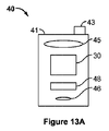
図13Aおよび図13Bは、複数の干渉変調器を含むディスプレイデバイス40を示すシステムブロック図の例を示している。ディスプレイデバイス40は、たとえば、スマートフォン、セルラー電話または携帯電話であり得る。ただし、ディスプレイデバイス40の同じ構成要素またはディスプレイデバイス40の軽微な変形も、テレビジョン、タブレット、電子リーダー、ハンドへルドデバイスおよびポータブルメディアプレーヤなど、様々なタイプのディスプレイデバイスを示す。
13A and 13B show example system block diagrams illustrating a
ディスプレイデバイス40は、ハウジング41と、ディスプレイ30と、アンテナ43と、スピーカー45と、入力デバイス48と、マイクロフォン46とを含む。ハウジング41は、射出成形および真空成形を含む様々な製造プロセスのうちのいずれかから形成され得る。さらに、ハウジング41は、限定はしないが、プラスチック、金属、ガラス、ゴム、およびセラミック、またはそれらの組合せを含む、様々な材料のうちのいずれかから製作され得る。ハウジング41は、異なる色の、または異なるロゴ、ピクチャ、もしくはシンボルを含んでいる、他の取外し可能な部分と交換され得る、取外し可能な部分(図示せず)を含むことができる。
The
ディスプレイ30は、本明細書で説明する、双安定またはアナログディスプレイを含む様々なディスプレイのうちのいずれかであり得る。ディスプレイ30はまた、プラズマ、EL、OLED、STN LCD、またはTFT LCDなど、フラットパネルディスプレイ、あるいはCRTまたは他の管デバイスなど、非フラットパネルディスプレイを含むように構成され得る。さらに、ディスプレイ30は、本明細書で説明する干渉変調器ディスプレイを含むことができる。
ディスプレイデバイス40の構成要素は図13Bに概略的に示されている。ディスプレイデバイス40は、ハウジング41を含み、それの中に少なくとも部分的に密閉された追加の構成要素を含むことができる。たとえば、ディスプレイデバイス40は、トランシーバ47に結合されたアンテナ43を含むネットワークインターフェース27を含む。トランシーバ47はプロセッサ21に接続され、プロセッサ21は調整ハードウェア52に接続される。調整ハードウェア52は、信号を調整する(たとえば、信号をフィルタ処理する)ように構成され得る。調整ハードウェア52は、スピーカー45およびマイクロフォン46に接続される。プロセッサ21は、入力デバイス48およびドライバコントローラ29にも接続される。ドライバコントローラ29は、フレームバッファ28に、およびアレイドライバ22に結合され、アレイドライバ22は次にディスプレイアレイ30に結合される。幾つかの実施態様では、電源50が、特定のディスプレイデバイス40設計における実質的にすべての構成要素に電力を与えることができる。
The components of
ネットワークインターフェース27は、ディスプレイデバイス40がネットワークを介して1つまたは複数のデバイスと通信することができるように、アンテナ43とトランシーバ47とを含む。ネットワークインターフェース27はまた、たとえば、プロセッサ21のデータ処理要件を軽減するための、何らかの処理能力を有し得る。アンテナ43は信号を送信および受信することができる。幾つかの実施態様では、アンテナ43は、IEEE16.11(a)、(b)、または(g)を含むIEEE16.11規格、あるいはIEEE802.11a、b、g、nおよびそれらのさらなる実施態様を含むIEEE802.11規格に従って、RF信号を送信および受信する。幾つかの他の実施態様では、アンテナ43は、BLUETOOTH規格に従ってRF信号を送信および受信する。セルラー電話の場合、アンテナ43は、3Gまたは4G技術を利用するシステムなどのワイヤレスネットワーク内で通信するために使用される、符号分割多元接続(CDMA)、周波数分割多元接続(FDMA)、時分割多元接続(TDMA)、Global System for Mobile communications(GSM(登録商標))、GSM/General Packet Radio Service(GPRS)、Enhanced Data GSM Environment(EDGE)、Terrestrial Trunked Radio(TETRA)、広帯域CDMA(W−CDMA(登録商標))、Evolution Data Optimized(EV−DO)、1xEV−DO、EV−DO Rev A、EV−DO Rev B、高速パケットアクセス(HSPA)、高速ダウンリンクパケットアクセス(HSDPA)、高速アップリンクパケットアクセス(HSUPA)、発展型高速パケットアクセス(HSPA+)、Long Term Evolution(LTE)、AMPS、または他の知られている信号を受信するように設計される。トランシーバ47は、アンテナ43から受信された信号がプロセッサ21によって受信され、プロセッサ21によってさらに操作され得るように、その信号を前処理することができる。トランシーバ47はまた、プロセッサ21から受信された信号がアンテナ43を介してディスプレイデバイス40から送信され得るように、その信号を処理することができる。
The
幾つかの実施態様では、トランシーバ47は受信機によって置き換えられ得る。さらに、幾つかの実施態様では、ネットワークインターフェース27は、プロセッサ21に送られるべき画像データを記憶または生成することができる画像ソースによって置き換えられ得る。プロセッサ21は、ディスプレイデバイス40の全体的な動作を制御することができる。プロセッサ21は、ネットワークインターフェース27または画像ソースから圧縮された画像データなどのデータを受信し、そのデータを生画像データに、または生画像データに容易に処理されるフォーマットに、処理する。プロセッサ21は、処理されたデータをドライバコントローラ29に、または記憶のためにフレームバッファ28に送ることができる。生データは、一般に、画像内の各ロケーションにおける画像特性を識別する情報を指す。たとえば、そのような画像特性は、色、飽和、およびグレースケールレベルを含むことができる。
In some implementations, the
プロセッサ21は、ディスプレイデバイス40の動作を制御するためのマイクロコントローラ、CPU、または論理ユニットを含むことができる。調整ハードウェア52は、スピーカー45に信号を送信するための、およびマイクロフォン46から信号を受信するための、増幅器およびフィルタを含み得る。調整ハードウェア52は、ディスプレイデバイス40内の個別構成要素であり得、あるいはプロセッサ21または他の構成要素内に組み込まれ得る。
The
ドライバコントローラ29は、プロセッサ21によって生成された生画像データをプロセッサ21から直接、またはフレームバッファ28から取ることができ、アレイドライバ22への高速送信のために適宜に生画像データを再フォーマットすることができる。幾つかの実施態様では、ドライバコントローラ29は、生画像データを、ラスタ様フォーマットを有するデータフローに再フォーマットすることができ、その結果、そのデータフローは、ディスプレイアレイ30にわたって走査するのに好適な時間順序を有する。次いで、ドライバコントローラ29は、フォーマットされた情報をアレイドライバ22に送る。LCDコントローラなどのドライバコントローラ29は、しばしば、スタンドアロン集積回路(IC)としてシステムプロセッサ21に関連付けられるが、そのようなコントローラは多くの方法で実施され得る。たとえば、コントローラは、ハードウェアとしてプロセッサ21中に埋め込まれるか、ソフトウェアとしてプロセッサ21中に埋め込まれるか、またはハードウェアにおいてアレイドライバ22と完全に一体化され得る。
The
アレイドライバ22は、ドライバコントローラ29からフォーマットされた情報を受信することができ、ビデオデータを波形の並列セットに再フォーマットすることができ、波形の並列セットは、ディスプレイのピクセルのx−y行列から来る、数百の、および時には数千の(またはより多くの)リード線に毎秒何回も適用される。
The
幾つかの実施態様では、ドライバコントローラ29、アレイドライバ22、およびディスプレイアレイ30は、本明細書で説明するディスプレイのタイプのうちのいずれにも適している。たとえば、ドライバコントローラ29は、従来のディスプレイコントローラまたは双安定ディスプレイコントローラ(IMODコントローラなど)であり得る。さらに、アレイドライバ22は、従来のドライバまたは双安定ディスプレイドライバ(IMODディスプレイドライバなど)であり得る。さらに、ディスプレイアレイ30は、従来のディスプレイアレイまたは双安定ディスプレイアレイ(IMODのアレイを含むディスプレイなど)とすることができる。幾つかの実施態様では、ドライバコントローラ29はアレイドライバ22と一体化することができる。そのような実施態様は、高集積システム、たとえば、携帯電話、ポータブル電子デバイス、腕時計または小面積ディスプレイにおいて、有用であることがある。
In some implementations,
幾つかの実施態様では、入力デバイス48は、たとえば、ユーザがディスプレイデバイス40の動作を制御できるように構成することができる。入力デバイス48は、QWERTYキーボードまたは電話キーパッドなどのキーパッド、ボタン、スイッチ、ロッカー、タッチセンシティブスクリーン、ディスプレイアレイ30と一体化されたタッチセンシティブスクリーン、あるいは感圧膜または感熱膜を含むことができる。マイクロフォン46は、ディスプレイデバイス40のための入力デバイスとして構成することができる。幾つかの実施態様では、ディスプレイデバイス40の動作を制御するために、マイクロフォン46を通してのボイスコマンドを用いることができる。
In some implementations, the
電源50は種々のエネルギー蓄積デバイスを含むことができる。たとえば、電源50は、ニッケルカドミウムバッテリまたはリチウムイオンバッテリなどの充電式バッテリとすることができる。充電式バッテリを使用する実施態様では、充電式バッテリは、たとえば、壁コンセントあるいは光起電性デバイスまたはアレイから来る電力を使用して充電可能な場合がある。代替的には、充電式バッテリはワイヤレス充電可能とすることができる。電源50はまた、再生可能エネルギー源、キャパシタ、あるいはプラスチック太陽電池または太陽電池塗料を含む太陽電池とすることもできる。電源50はまた、壁コンセントから電力を受け取るように構成することもできる。
The
幾つかの実施態様では、制御プログラマビリティがドライバコントローラ29中に存在し、これは電子ディスプレイシステム中の幾つかの場所に配置され得る。幾つかの他の実施態様では、制御プログラマビリティがアレイドライバ22中に存在する。上記で説明した最適化は、任意の数のハードウェアおよび/またはソフトウェア構成要素において、ならびに様々な構成において実施され得る。
In some implementations, control programmability exists in the
本明細書で開示する実施態様に関して説明した様々な例示的な論理、論理ブロック、モジュール、回路、およびアルゴリズムステップは、電子ハードウェア、コンピュータソフトウェア、または両方の組合せとして実施され得る。ハードウェアとソフトウェアの互換性が、概して機能に関して説明され、上記で説明した様々な例示的な構成要素、ブロック、モジュール、回路およびステップにおいて示された。そのような機能がハードウェアで実施されるか、ソフトウェアで実施されるかは、特定の適用例および全体的なシステムに課された設計制約に依存する。 Various exemplary logic, logic blocks, modules, circuits, and algorithm steps described in connection with the embodiments disclosed herein may be implemented as electronic hardware, computer software, or a combination of both. Hardware and software compatibility has been generally described in terms of functionality and has been illustrated in various exemplary components, blocks, modules, circuits, and steps described above. Whether such functionality is implemented in hardware or software depends upon the particular application and design constraints imposed on the overall system.
本明細書で開示する態様に関して説明した様々な例示的な論理、論理ブロック、モジュール、および回路を実施するために使用される、ハードウェアおよびデータ処理装置は、汎用シングルチップまたはマルチチッププロセッサ、デジタル信号プロセッサ(DSP)、特定用途向け集積回路(ASIC)、フィールドプログラマブルゲートアレイ(FPGA)または他のプログラマブル論理デバイス、個別ゲートまたはトランジスタ論理、個別ハードウェア構成要素、あるいは本明細書で説明した機能を実行するように設計されたそれらの任意の組合せを用いて実施または実行され得る。汎用プロセッサは、マイクロプロセッサ、あるいは任意の従来のプロセッサ、コントローラ、マイクロコントローラ、または状態機械であり得る。プロセッサは、コンピューティングデバイスの組合せ、たとえば、DSPとマイクロプロセッサとの組合せ、複数のマイクロプロセッサ、DSPコアと連携する1つまたは複数のマイクロプロセッサ、あるいは任意の他のそのような構成として実施することもできる。幾つかの実施態様では、特定のステップおよび方法が、所与の機能に固有である回路によって実行され得る。 The hardware and data processing devices used to implement the various exemplary logic, logic blocks, modules, and circuits described with respect to the aspects disclosed herein can be general purpose single-chip or multi-chip processors, digital Signal processor (DSP), application specific integrated circuit (ASIC), field programmable gate array (FPGA) or other programmable logic device, individual gate or transistor logic, individual hardware components, or functions described herein It can be implemented or implemented using any combination thereof designed to perform. A general purpose processor may be a microprocessor, or any conventional processor, controller, microcontroller, or state machine. The processor may be implemented as a combination of computing devices, eg, a combination of a DSP and a microprocessor, a plurality of microprocessors, one or more microprocessors associated with a DSP core, or any other such configuration. You can also. In some implementations, certain steps and methods may be performed by circuitry that is specific to a given function.
1つまたは複数の態様では、説明した機能は、本明細書で開示する構造を含むハードウェア、デジタル電子回路、コンピュータソフトウェア、ファームウェア、およびそれらの上記構造の構造的等価物において、またはそれらの任意の組合せにおいて実施され得る。また、本明細書で説明した主題の実施態様は、1つまたは複数のコンピュータプログラムとして、すなわち、データ処理装置が実行するためにコンピュータ記憶媒体上に符号化された、またはデータ処理装置の動作を制御するための、コンピュータプログラム命令の1つまたは複数のモジュールとして、実施され得る。 In one or more aspects, the functions described may be in hardware, digital electronic circuitry, computer software, firmware, and structural equivalents of the above structures, or any of them, including the structures disclosed herein. Can be implemented in combination. Also, embodiments of the subject matter described in this specification can be implemented as one or more computer programs, ie, encoded on a computer storage medium for execution by a data processing device, or operations of a data processing device. It may be implemented as one or more modules of computer program instructions for controlling.
本開示で説明した実施態様への様々な修正は当業者には容易に明らかであり得、本明細書で定義した一般原理は、本開示の趣旨または範囲から逸脱することなく他の実施態様に適用され得る。したがって、特許請求の範囲は、本明細書で示した実施態様に限定されるものではなく、本開示と、本明細書で開示する原理および新規の特徴とに一致する、最も広い範囲を与られるべきである。「例示的」という単語は、本明細書ではもっぱら「例、事例、または例示の働きをすること」を意味するために使用される。本明細書に「例示的」と記載されたいかなる実施態様も、必ずしも他の可能性または実施態様よりも好ましいまたは有利であると解釈されるべきではない。さらに、「上側」および「下側」という用語は、図の説明を簡単にするために時々使用され、適切に配向されたページ上の図の配向に対応する相対位置を示すが、実施されたIMODの適切な配向を反映しないことがあることを、当業者は容易に諒解されよう。 Various modifications to the embodiments described in this disclosure will be readily apparent to those skilled in the art, and the general principles defined herein may be used in other embodiments without departing from the spirit or scope of this disclosure. Can be applied. Accordingly, the claims are not limited to the embodiments shown herein but are to be accorded the widest scope consistent with the present disclosure and the principles and novel features disclosed herein. Should. The word “exemplary” is used herein exclusively to mean “serving as an example, instance, or illustration”. Any embodiment described herein as "exemplary" is not necessarily to be construed as preferred or advantageous over other possibilities or embodiments. In addition, the terms “upper” and “lower” are sometimes used to simplify the description of the figure and indicate the relative position corresponding to the orientation of the figure on a properly oriented page, although implemented. One skilled in the art will readily appreciate that it may not reflect the proper orientation of the IMOD.
また、別個の実施態様に関して本明細書で説明された幾つかの特徴は、単一の実施態様において組合せで実施され得る。また、逆に、単一の実施態様に関して説明した様々な特徴は、複数の実施態様において別個に、あるいは任意の好適な部分組合せで実施され得る。その上、特徴は、幾つかの組合せで働くものとして上記で説明され、初めにそのように請求されることさえあるが、請求される組合せからの1つまたは複数の特徴は、場合によってはその組合せから削除され得、請求される組合せは、部分組合せ、または部分組合せの変形形態を対象とし得る。 Also, some features described herein with respect to separate embodiments can be implemented in combination in a single embodiment. Conversely, various features described with respect to a single embodiment can be implemented in multiple embodiments separately or in any suitable subcombination. Moreover, a feature is described above as working in several combinations and may even be so claimed initially, but one or more features from the claimed combination may in some cases be Combinations that may be deleted from the combination and claimed combinations may be directed to subcombinations, or variations of subcombinations.
同様に、動作は特定の順序で図面に示されているが、そのような動作は、望ましい結果を達成するために、示される特定の順序でまたは順番に実行される必要がないこと、またはすべての例示される動作が実行される必要があるとは限らないことは、当業者は容易に認識されよう。さらに、図面は、流れ図の形態でもう1つの例示的なプロセスを概略的に示し得る。ただし、図示されていない他の動作が、概略的に示される例示的なプロセスに組み込まれ得る。たとえば、1つまたは複数の追加の動作が、図示の動作のうちのいずれかの前に、後に、同時に、またはそれの間で、実行され得る。幾つかの状況では、マルチタスキングおよび並列処理が有利であり得る。その上、上記で説明した実施態様における様々なシステム構成要素の分離は、すべての実施態様においてそのような分離を必要とするものとして理解されるべきでなく、説明するプログラム構成要素およびシステムは、概して、単一のソフトウェア製品において互いに一体化されるか、または複数のソフトウェア製品にパッケージングされ得ることを理解されたい。さらに、他の実施態様が以下の特許請求の範囲内に入る。場合によっては、特許請求の範囲に記載の行為は、異なる順序で実行され、依然として望ましい結果を達成することができる。 Similarly, operations are shown in the drawings in a particular order, but such operations need not be performed in the particular order shown or in order, or all, to achieve the desired result. Those skilled in the art will readily recognize that the illustrated operations need not necessarily be performed. Furthermore, the drawings may schematically show another exemplary process in the form of a flowchart. However, other operations not shown may be incorporated into the exemplary process schematically shown. For example, one or more additional operations may be performed before, after, simultaneously with, or between any of the illustrated operations. In some situations, multitasking and parallel processing may be advantageous. Moreover, the separation of various system components in the embodiments described above should not be understood as requiring such separation in all embodiments, and the program components and systems described are: In general, it should be understood that they can be integrated together in a single software product or packaged into multiple software products. Furthermore, other embodiments are within the scope of the following claims. In some cases, the actions recited in the claims can be performed in a different order and still achieve desirable results.
12 干渉変調器、IMOD、ピクセル
13、15 光
14 可動反射層、層、反射層
14a 反射副層、伝導性層、副層
14b 支持層、誘電支持層、副層
14c 伝導性層、副層
16 光学スタック、層
16a 吸収層、光吸収体、副層、導体/吸収体副層
16b 誘電体、副層
18 ポスト、支持体、支持ポスト
19 ギャップ、キャビティ
20 透明基板、基板
21 プロセッサ、システムプロセッサ
22 アレイドライバ
23 ブラックマスク構造
24 行ドライバ回路
25 犠牲層、犠牲材料
26 列ドライバ回路
27 ネットワークインターフェース
28 フレームバッファ
29 ドライバコントローラ
30 ディスプレイアレイ、パネル、ディスプレイ
32 テザー
34 変形可能層
35 スペーサ層
40 ディスプレイデバイス
41 ハウジング
43 アンテナ
45 スピーカー
46 マイクロフォン
47 トランシーバ
48 入力デバイス
50 電源
52 調整ハードウェア
60a 第1のライン時間、ライン時間
60b 第2のライン時間、ライン時間
60c 第3のライン時間、ライン時間
60d 第4のライン時間、ライン時間
60e ライン時間、第5のライン時間
62 高いセグメント電圧
64 低いセグメント電圧
70 開放電圧
72 高い保持電圧
74 高いアドレス電圧
76 低い保持電圧
78 低いアドレス電圧
1000 スタックビア構造
1002 基板
1004 第1の金属層
1006 第1の誘電体層
1008 第2の金属層
1010 第2の誘電体層
1012 基板1002の中心部分
1013 第3の金属層
1014 周辺部分
1038 角度
1052 平面部分
1054 傾斜部分
1100 装置
1102、1122、1142 第1のスタックビア構造の中心部分
1104、1114、1124 伝導性トレース
1112、1132 第2のスタックビア構造の中心部分
1202 第1のスタックビア構造、スタックビア構造、第1のビア構造
1204 第2のスタックビア構造、スタックビア構造
1206 第1のデバイス
12 Interferometric Modulator, IMOD, Pixel 13, 15 Light 14 Movable Reflective Layer, Layer, Reflective Layer 14a Reflective Sublayer, Conductive Layer, Sublayer 14b Support Layer, Dielectric Support Layer, Sublayer 14c Conductive Layer, Sublayer 16 Optical stack, layer 16a absorbing layer, light absorber, sublayer, conductor / absorber sublayer 16b dielectric, sublayer 18 post, support, support post 19 gap, cavity 20 transparent substrate, substrate 21 processor, system processor 22 Array Driver 23 Black Mask Structure 24 Row Driver Circuit 25 Sacrificial Layer, Sacrificial Material 26 Column Driver Circuit 27 Network Interface 28 Frame Buffer 29 Driver Controller 30 Display Array, Panel, Display 32 Tether 34 Deformable Layer 35 Spacer Layer 40 Display Device 41 House 43 Antenna 45 Speaker 46 Microphone 47 Transceiver 48 Input device 50 Power supply 52 Adjustment hardware 60a First line time, line time 60b Second line time, line time 60c Third line time, line time 60d Fourth line Time, line time 60e line time, fifth line time 62 high segment voltage 64 low segment voltage 70 open voltage 72 high holding voltage 74 high address voltage 76 low holding voltage 78 low address voltage 1000 stack via structure 1002 substrate 1004 first Metal layer 1006 First dielectric layer 1008 Second metal layer 1010 Second dielectric layer 1012 Central portion of substrate 1002 1013 Third metal layer 1014 Peripheral portion 1038 Angle 1052 Plane portion 105 Inclined portion 1100 Device 1102, 1122, 1142 Central portion of first stacked via structure 1104, 1114, 1124 Conductive trace 1112, 1132 Central portion of second stacked via structure 1202 First stacked via structure, stacked via structure, First via structure 1204 Second stacked via structure, stacked via structure 1206 First device
Claims (20)
前記基板の表面上の第1の電気機械システム(EMS)デバイスであって、第1の金属層と第2の金属層とを含む第1のEMSデバイスと、
前記基板の前記表面上の第1のビア構造であって、前記第1の金属層と、前記第2の金属層と、第3の金属層とを含み、前記第2の金属層が、前記第1の金属層上に配設され、前記第3の金属層が、前記第1のビア構造の中心部分において前記第2の金属層上に配設される、第1のビア構造と
を備え、
前記第1のEMSデバイスの前記第1の金属層が、前記第1のビア構造の前記第1の金属層に結合され、前記第1のEMSデバイスの前記第1の金属層、および前記第1のビア構造の前記第1の金属層は、同じ金属層である、装置。 A substrate,
A first electromechanical system (EMS) device on a surface of the substrate, the first EMS device including a first metal layer and a second metal layer;
A first via structure on the surface of the substrate, comprising the first metal layer, the second metal layer, and a third metal layer, wherein the second metal layer comprises: A first via structure disposed on the first metal layer, wherein the third metal layer is disposed on the second metal layer at a central portion of the first via structure. ,
The first metal layer of the first EMS device is coupled to the first metal layer of the first via structure, the first metal layer of the first EMS device, and the first The device wherein the first metal layer of the via structure is the same metal layer.
をさらに備える、請求項1から8のいずれか一項に記載の装置。 A plurality of dielectric layers between the metal layers in a peripheral portion of the first via structure, wherein the central portion of the first via structure does not include the peripheral portion of the first via structure; 9. The device according to any one of claims 1 to 8, further comprising a plurality of dielectric layers.
をさらに備える、請求項1から9のいずれか一項に記載の装置。 A plurality of via structures on the surface of the substrate, the first via structure and a second via structure, wherein the second via structure includes the second metal layer and the third via structure; 10. A metal layer, wherein the third metal layer further comprises a plurality of via structures disposed on the second metal layer at a central portion of the second via structure. The apparatus as described in any one of.
前記ディスプレイと通信するように構成され、画像データを処理するように構成されたプロセッサと、
前記プロセッサと通信するように構成されたメモリデバイスと
をさらに備える、請求項1から12のいずれか一項に記載の装置。 Display,
A processor configured to communicate with the display and configured to process image data;
The apparatus of any one of claims 1 to 12, further comprising a memory device configured to communicate with the processor.
前記ドライバ回路に前記画像データの少なくとも一部分を送るように構成されたコントローラと
をさらに備える、請求項13に記載の装置。 A driver circuit configured to send at least one signal to the display;
14. The apparatus of claim 13, further comprising a controller configured to send at least a portion of the image data to the driver circuit.
をさらに備える、請求項13に記載の装置。 14. The image source module configured to send the image data to the processor, further comprising an image source module comprising at least one of a receiver, a transceiver, and a transmitter. apparatus.
をさらに備える、請求項13に記載の装置。 The apparatus of claim 13, further comprising an input device configured to receive input data and communicate the input data to the processor.
前記基板の表面上の第1の電気機械システム(EMS)デバイスであって、第1の金属層と第2の金属層とを含む第1のEMSデバイスと、
前記基板の前記表面上の第1のビア構造であって、前記第1の金属層と、前記第2の金属層と、第3の金属層と、第4の金属層とを含み、前記第2の金属層が、前記第1の金属層上に配設され、前記第3の金属層が、前記第2の金属層上に配設され、前記第4の金属層が、前記第1のビア構造の中心部分において前記第3の金属層上に配設される、第1のビア構造と
を備え、
前記第1のEMSデバイスの前記第1の金属層が、前記第1のビア構造の前記第1の金属層に結合され、前記第1のEMSデバイスの前記第1の金属層、および前記第1のビア構造の前記第1の金属層が、同じ金属層である、装置。 A substrate,
A first electromechanical system (EMS) device on a surface of the substrate, the first EMS device including a first metal layer and a second metal layer;
A first via structure on the surface of the substrate, the first via layer including the first metal layer, the second metal layer, a third metal layer, and a fourth metal layer; Two metal layers are disposed on the first metal layer, the third metal layer is disposed on the second metal layer, and the fourth metal layer is disposed on the first metal layer. A first via structure disposed on the third metal layer in a central portion of the via structure;
The first metal layer of the first EMS device is coupled to the first metal layer of the first via structure, the first metal layer of the first EMS device, and the first The device in which the first metal layer of the via structure is the same metal layer.
をさらに備える、請求項17または18に記載の装置。 A plurality of via structures, including the first via structure and the second via structure, wherein the second via structure includes the second metal layer, the third metal layer, and the second metal layer; 4, wherein the third metal layer is disposed on the second metal layer, and the fourth metal layer is disposed in the central portion of the second via structure. The apparatus of claim 17 or 18, further comprising a plurality of via structures disposed on the metal layer.
Applications Claiming Priority (3)
| Application Number | Priority Date | Filing Date | Title |
|---|---|---|---|
| US13/278,080 | 2011-10-20 | ||
| US13/278,080 US10131534B2 (en) | 2011-10-20 | 2011-10-20 | Stacked vias for vertical integration |
| PCT/US2012/060648 WO2013059345A1 (en) | 2011-10-20 | 2012-10-17 | Stacked vias for vertical integration |
Publications (1)
| Publication Number | Publication Date |
|---|---|
| JP2014534470A true JP2014534470A (en) | 2014-12-18 |
Family
ID=47138180
Family Applications (1)
| Application Number | Title | Priority Date | Filing Date |
|---|---|---|---|
| JP2014537185A Pending JP2014534470A (en) | 2011-10-20 | 2012-10-17 | Stack via for vertical integration |
Country Status (7)
| Country | Link |
|---|---|
| US (1) | US10131534B2 (en) |
| EP (1) | EP2768767A1 (en) |
| JP (1) | JP2014534470A (en) |
| KR (1) | KR20140083042A (en) |
| CN (2) | CN110228785A (en) |
| IN (1) | IN2014CN02998A (en) |
| WO (1) | WO2013059345A1 (en) |
Families Citing this family (3)
| Publication number | Priority date | Publication date | Assignee | Title |
|---|---|---|---|---|
| US20180123245A1 (en) * | 2016-10-28 | 2018-05-03 | Broadcom Corporation | Broadband antenna array for wireless communications |
| CN108231747A (en) * | 2016-12-21 | 2018-06-29 | 中芯国际集成电路制造(上海)有限公司 | Semiconductor devices and preparation method thereof, electronic device |
| EP3598235A1 (en) * | 2018-07-18 | 2020-01-22 | ASML Netherlands B.V. | Metrology apparatus and method for determining a characteristic relating to one or more structures on a substrate |
Citations (10)
| Publication number | Priority date | Publication date | Assignee | Title |
|---|---|---|---|---|
| JP2004335506A (en) * | 2003-04-30 | 2004-11-25 | Victor Co Of Japan Ltd | Multilayer printed wiring board |
| JP2006090740A (en) * | 2004-09-21 | 2006-04-06 | Ngk Spark Plug Co Ltd | Method of inspecting wiring board, method of manufacturing wiring board device for and inspecting wiring board |
| JP2006263902A (en) * | 2005-02-25 | 2006-10-05 | Hitachi Ltd | Integrated micro electromechanical system, and manufacturing method thereof |
| JP2009124318A (en) * | 2007-11-13 | 2009-06-04 | Rohm Co Ltd | Semiconductor device |
| JP2009170669A (en) * | 2008-01-16 | 2009-07-30 | Fujitsu Microelectronics Ltd | Wiring board, and semiconductor device |
| JP2009188402A (en) * | 2008-02-04 | 2009-08-20 | Agilent Technol Inc | Hermetically-packaged devices, and methods for hermetically packaging at least one device at wafer level |
| JP2010067647A (en) * | 2008-09-08 | 2010-03-25 | Oki Semiconductor Co Ltd | Manufacturing method for semiconductor device |
| JP2010156704A (en) * | 2010-02-18 | 2010-07-15 | Hokuriku Electric Ind Co Ltd | Piezoelectric triaxial acceleration sensor |
| JP2010535641A (en) * | 2007-08-07 | 2010-11-25 | クォルコム・メムズ・テクノロジーズ・インコーポレーテッド | MEMS device and wiring thereof |
| JP2010283189A (en) * | 2009-06-05 | 2010-12-16 | Shinko Electric Ind Co Ltd | Wiring board and method of manufacturing the same |
Family Cites Families (19)
| Publication number | Priority date | Publication date | Assignee | Title |
|---|---|---|---|---|
| US5798283A (en) | 1995-09-06 | 1998-08-25 | Sandia Corporation | Method for integrating microelectromechanical devices with electronic circuitry |
| US5917645A (en) * | 1997-03-28 | 1999-06-29 | Daewoo Electronics Co., Ltd. | Thin film actuated mirror array in an optical projection system and method for manufacturing the same |
| US6320244B1 (en) * | 1999-01-12 | 2001-11-20 | Agere Systems Guardian Corp. | Integrated circuit device having dual damascene capacitor |
| US6562656B1 (en) | 2001-06-25 | 2003-05-13 | Thin Film Module, Inc. | Cavity down flip chip BGA |
| US20030234415A1 (en) * | 2002-06-24 | 2003-12-25 | Hwey-Ching Chien | Scalable three-dimensional fringe capacitor with stacked via |
| US20050041405A1 (en) | 2003-08-22 | 2005-02-24 | Intel Corporation | Stacked via structure that includes a skip via |
| US7081647B2 (en) | 2003-09-29 | 2006-07-25 | Matsushita Electric Industrial Co., Ltd. | Microelectromechanical system and method for fabricating the same |
| JP4608294B2 (en) | 2004-11-30 | 2011-01-12 | 日亜化学工業株式会社 | RESIN MOLDED BODY, SURFACE MOUNTED LIGHT EMITTING DEVICE AND METHOD FOR PRODUCING THEM |
| KR100881303B1 (en) * | 2005-11-02 | 2009-02-03 | 이비덴 가부시키가이샤 | Multilayer printed wiring board for semiconductor device and process for producing the same |
| TWI298608B (en) | 2006-05-19 | 2008-07-01 | Foxconn Advanced Tech Inc | Method for manufacturing stack via of hdi printed circuit board |
| US7777715B2 (en) | 2006-06-29 | 2010-08-17 | Qualcomm Mems Technologies, Inc. | Passive circuits for de-multiplexing display inputs |
| US20080029898A1 (en) | 2006-08-01 | 2008-02-07 | Farooq Mukta G | Via stack structures |
| US7733552B2 (en) | 2007-03-21 | 2010-06-08 | Qualcomm Mems Technologies, Inc | MEMS cavity-coating layers and methods |
| US8022896B2 (en) * | 2007-08-08 | 2011-09-20 | Qualcomm Mems Technologies, Inc. | ESD protection for MEMS display panels |
| US8242593B2 (en) | 2008-01-27 | 2012-08-14 | International Business Machines Corporation | Clustered stacked vias for reliable electronic substrates |
| CN101728355A (en) | 2008-11-03 | 2010-06-09 | 巨擘科技股份有限公司 | Guide hole structure of multilayer substrate and manufacturing method thereof |
| WO2010114687A1 (en) * | 2009-03-30 | 2010-10-07 | Megica Corporation | Integrated circuit chip using top post-passivation technology and bottom structure technology |
| TW201102340A (en) * | 2009-07-10 | 2011-01-16 | Nat Univ Tsing Hua | A method for fabricating a multilayer microstructure with balancing residual stress capability |
| CN102001613B (en) | 2009-09-02 | 2014-10-22 | 原相科技股份有限公司 | Microelectronic device and manufacturing method thereof, and micro electromechanical packaging structure and packaging method thereof |
-
2011
- 2011-10-20 US US13/278,080 patent/US10131534B2/en active Active
-
2012
- 2012-10-17 WO PCT/US2012/060648 patent/WO2013059345A1/en active Application Filing
- 2012-10-17 JP JP2014537185A patent/JP2014534470A/en active Pending
- 2012-10-17 KR KR1020147013565A patent/KR20140083042A/en not_active Application Discontinuation
- 2012-10-17 CN CN201910414865.5A patent/CN110228785A/en active Pending
- 2012-10-17 IN IN2998CHN2014 patent/IN2014CN02998A/en unknown
- 2012-10-17 CN CN201280059040.2A patent/CN103974896A/en active Pending
- 2012-10-17 EP EP12781228.7A patent/EP2768767A1/en not_active Withdrawn
Patent Citations (10)
| Publication number | Priority date | Publication date | Assignee | Title |
|---|---|---|---|---|
| JP2004335506A (en) * | 2003-04-30 | 2004-11-25 | Victor Co Of Japan Ltd | Multilayer printed wiring board |
| JP2006090740A (en) * | 2004-09-21 | 2006-04-06 | Ngk Spark Plug Co Ltd | Method of inspecting wiring board, method of manufacturing wiring board device for and inspecting wiring board |
| JP2006263902A (en) * | 2005-02-25 | 2006-10-05 | Hitachi Ltd | Integrated micro electromechanical system, and manufacturing method thereof |
| JP2010535641A (en) * | 2007-08-07 | 2010-11-25 | クォルコム・メムズ・テクノロジーズ・インコーポレーテッド | MEMS device and wiring thereof |
| JP2009124318A (en) * | 2007-11-13 | 2009-06-04 | Rohm Co Ltd | Semiconductor device |
| JP2009170669A (en) * | 2008-01-16 | 2009-07-30 | Fujitsu Microelectronics Ltd | Wiring board, and semiconductor device |
| JP2009188402A (en) * | 2008-02-04 | 2009-08-20 | Agilent Technol Inc | Hermetically-packaged devices, and methods for hermetically packaging at least one device at wafer level |
| JP2010067647A (en) * | 2008-09-08 | 2010-03-25 | Oki Semiconductor Co Ltd | Manufacturing method for semiconductor device |
| JP2010283189A (en) * | 2009-06-05 | 2010-12-16 | Shinko Electric Ind Co Ltd | Wiring board and method of manufacturing the same |
| JP2010156704A (en) * | 2010-02-18 | 2010-07-15 | Hokuriku Electric Ind Co Ltd | Piezoelectric triaxial acceleration sensor |
Also Published As
| Publication number | Publication date |
|---|---|
| KR20140083042A (en) | 2014-07-03 |
| CN110228785A (en) | 2019-09-13 |
| EP2768767A1 (en) | 2014-08-27 |
| CN103974896A (en) | 2014-08-06 |
| US10131534B2 (en) | 2018-11-20 |
| WO2013059345A1 (en) | 2013-04-25 |
| IN2014CN02998A (en) | 2015-07-03 |
| US20130100143A1 (en) | 2013-04-25 |
Similar Documents
| Publication | Publication Date | Title |
|---|---|---|
| TWI484566B (en) | Amorphous oxide semiconductor thin film transistor fabrication method | |
| JP5696216B2 (en) | Mirrors with improved dielectric properties for IMOD displays | |
| JP2014517930A (en) | Wiring and peripherals for integrated capacitive touch devices | |
| JP6131268B2 (en) | Inclined facets for display devices | |
| JP5642912B1 (en) | Matching layer thin films for electromechanical system reflective display devices | |
| JP2014508958A (en) | Electromechanical interferometric modulator device | |
| JP2015522840A (en) | Integration of thin film switching devices with electromechanical system devices | |
| JP2014529802A (en) | Capacitive touch sensor with light shielding structure | |
| JP2015522851A (en) | Cavity liner for electromechanical system devices | |
| JP5752334B2 (en) | Electromechanical system devices | |
| JP2015503114A (en) | Electromechanical system devices | |
| JP5687402B1 (en) | Analog IMOD with color notch filter | |
| JP5801424B2 (en) | Inactive dummy pixel | |
| JP2014510950A (en) | Method and apparatus for line time reduction | |
| JP2014534470A (en) | Stack via for vertical integration | |
| JP2014519050A (en) | Mechanical layer and method of making it | |
| JP2015501943A (en) | Side wall spacers along conductive lines | |
| TW201333530A (en) | Electromechanical systems variable capacitance device | |
| TW201337326A (en) | Storage capacitor for electromechanical systems and methods of forming the same | |
| JP5792373B2 (en) | Pixel via (PIXELVIA) and method of forming the same | |
| TW201329602A (en) | Electromechanical systems variable capacitance device | |
| JP2015519594A (en) | Multi-state IMOD with RGB absorber | |
| JP2015507215A (en) | Encapsulated array of electromechanical system devices | |
| JP5745702B2 (en) | Method and circuit for driving a display including a plurality of segment lines | |
| JP2014512554A (en) | Apparatus and method for supporting a mechanical layer |
Legal Events
| Date | Code | Title | Description |
|---|---|---|---|
| A131 | Notification of reasons for refusal |
Free format text: JAPANESE INTERMEDIATE CODE: A131 Effective date: 20150706 |
|
| A521 | Written amendment |
Free format text: JAPANESE INTERMEDIATE CODE: A523 Effective date: 20151006 |
|
| A131 | Notification of reasons for refusal |
Free format text: JAPANESE INTERMEDIATE CODE: A131 Effective date: 20160314 |
|
| A02 | Decision of refusal |
Free format text: JAPANESE INTERMEDIATE CODE: A02 Effective date: 20161017 |