JP2014508317A - 基板転移単結晶ブラッグミラー - Google Patents
基板転移単結晶ブラッグミラー Download PDFInfo
- Publication number
- JP2014508317A JP2014508317A JP2013549852A JP2013549852A JP2014508317A JP 2014508317 A JP2014508317 A JP 2014508317A JP 2013549852 A JP2013549852 A JP 2013549852A JP 2013549852 A JP2013549852 A JP 2013549852A JP 2014508317 A JP2014508317 A JP 2014508317A
- Authority
- JP
- Japan
- Prior art keywords
- carrier substrate
- stack
- type
- substrate
- mirror
- Prior art date
- Legal status (The legal status is an assumption and is not a legal conclusion. Google has not performed a legal analysis and makes no representation as to the accuracy of the status listed.)
- Granted
Links
- 239000000758 substrate Substances 0.000 title claims abstract description 106
- 239000013078 crystal Substances 0.000 title claims description 38
- 230000007704 transition Effects 0.000 title description 4
- 239000004065 semiconductor Substances 0.000 claims abstract description 19
- 230000003287 optical effect Effects 0.000 claims description 39
- 238000000034 method Methods 0.000 claims description 31
- 238000010521 absorption reaction Methods 0.000 claims description 18
- 230000008569 process Effects 0.000 claims description 17
- 238000004519 manufacturing process Methods 0.000 claims description 13
- 238000005259 measurement Methods 0.000 claims description 10
- 125000006850 spacer group Chemical group 0.000 claims description 10
- 238000000137 annealing Methods 0.000 claims description 9
- 238000005411 Van der Waals force Methods 0.000 claims description 8
- 230000000712 assembly Effects 0.000 claims description 8
- 238000000429 assembly Methods 0.000 claims description 8
- 229910004298 SiO 2 Inorganic materials 0.000 claims description 7
- 239000011521 glass Substances 0.000 claims description 7
- 238000001451 molecular beam epitaxy Methods 0.000 claims description 7
- 229910052594 sapphire Inorganic materials 0.000 claims description 6
- 239000010980 sapphire Substances 0.000 claims description 6
- 238000002488 metal-organic chemical vapour deposition Methods 0.000 claims description 5
- 229910001218 Gallium arsenide Inorganic materials 0.000 claims description 4
- 229910002058 ternary alloy Inorganic materials 0.000 claims description 4
- 229910052751 metal Inorganic materials 0.000 claims description 2
- 239000002184 metal Substances 0.000 claims description 2
- 238000000927 vapour-phase epitaxy Methods 0.000 claims description 2
- 229910000980 Aluminium gallium arsenide Inorganic materials 0.000 claims 2
- FTWRSWRBSVXQPI-UHFFFAOYSA-N alumanylidynearsane;gallanylidynearsane Chemical compound [As]#[Al].[As]#[Ga] FTWRSWRBSVXQPI-UHFFFAOYSA-N 0.000 description 10
- 239000010408 film Substances 0.000 description 10
- 239000000463 material Substances 0.000 description 10
- 238000002310 reflectometry Methods 0.000 description 6
- 230000000694 effects Effects 0.000 description 5
- JBRZTFJDHDCESZ-UHFFFAOYSA-N AsGa Chemical compound [As]#[Ga] JBRZTFJDHDCESZ-UHFFFAOYSA-N 0.000 description 4
- 230000007547 defect Effects 0.000 description 4
- 238000013017 mechanical damping Methods 0.000 description 4
- 238000005498 polishing Methods 0.000 description 4
- 230000035945 sensitivity Effects 0.000 description 4
- 239000000853 adhesive Substances 0.000 description 3
- 230000001070 adhesive effect Effects 0.000 description 3
- 229910052782 aluminium Inorganic materials 0.000 description 3
- XAGFODPZIPBFFR-UHFFFAOYSA-N aluminium Chemical compound [Al] XAGFODPZIPBFFR-UHFFFAOYSA-N 0.000 description 3
- 239000011248 coating agent Substances 0.000 description 3
- 238000000576 coating method Methods 0.000 description 3
- CJNBYAVZURUTKZ-UHFFFAOYSA-N hafnium(IV) oxide Inorganic materials O=[Hf]=O CJNBYAVZURUTKZ-UHFFFAOYSA-N 0.000 description 3
- 238000001659 ion-beam spectroscopy Methods 0.000 description 3
- 238000004943 liquid phase epitaxy Methods 0.000 description 3
- 239000012071 phase Substances 0.000 description 3
- 230000009467 reduction Effects 0.000 description 3
- JMASRVWKEDWRBT-UHFFFAOYSA-N Gallium nitride Chemical compound [Ga]#N JMASRVWKEDWRBT-UHFFFAOYSA-N 0.000 description 2
- GPXJNWSHGFTCBW-UHFFFAOYSA-N Indium phosphide Chemical compound [In]#P GPXJNWSHGFTCBW-UHFFFAOYSA-N 0.000 description 2
- VYPSYNLAJGMNEJ-UHFFFAOYSA-N Silicium dioxide Chemical compound O=[Si]=O VYPSYNLAJGMNEJ-UHFFFAOYSA-N 0.000 description 2
- 230000009286 beneficial effect Effects 0.000 description 2
- 230000005540 biological transmission Effects 0.000 description 2
- 238000000151 deposition Methods 0.000 description 2
- 230000008021 deposition Effects 0.000 description 2
- 229910052732 germanium Inorganic materials 0.000 description 2
- GNPVGFCGXDBREM-UHFFFAOYSA-N germanium atom Chemical compound [Ge] GNPVGFCGXDBREM-UHFFFAOYSA-N 0.000 description 2
- 238000010438 heat treatment Methods 0.000 description 2
- 230000006872 improvement Effects 0.000 description 2
- 238000005468 ion implantation Methods 0.000 description 2
- 230000031700 light absorption Effects 0.000 description 2
- 238000000926 separation method Methods 0.000 description 2
- 229910052710 silicon Inorganic materials 0.000 description 2
- 239000010703 silicon Substances 0.000 description 2
- 238000004611 spectroscopical analysis Methods 0.000 description 2
- 239000000126 substance Substances 0.000 description 2
- 238000001039 wet etching Methods 0.000 description 2
- PIGFYZPCRLYGLF-UHFFFAOYSA-N Aluminum nitride Chemical compound [Al]#N PIGFYZPCRLYGLF-UHFFFAOYSA-N 0.000 description 1
- 238000012935 Averaging Methods 0.000 description 1
- 229910002601 GaN Inorganic materials 0.000 description 1
- 241000588731 Hafnia Species 0.000 description 1
- 229910045601 alloy Inorganic materials 0.000 description 1
- 239000000956 alloy Substances 0.000 description 1
- 238000013459 approach Methods 0.000 description 1
- 229910052785 arsenic Inorganic materials 0.000 description 1
- RQNWIZPPADIBDY-UHFFFAOYSA-N arsenic atom Chemical compound [As] RQNWIZPPADIBDY-UHFFFAOYSA-N 0.000 description 1
- 230000008859 change Effects 0.000 description 1
- 210000001520 comb Anatomy 0.000 description 1
- PMHQVHHXPFUNSP-UHFFFAOYSA-M copper(1+);methylsulfanylmethane;bromide Chemical compound Br[Cu].CSC PMHQVHHXPFUNSP-UHFFFAOYSA-M 0.000 description 1
- 230000008878 coupling Effects 0.000 description 1
- 238000010168 coupling process Methods 0.000 description 1
- 238000005859 coupling reaction Methods 0.000 description 1
- 238000013016 damping Methods 0.000 description 1
- 230000001747 exhibiting effect Effects 0.000 description 1
- 238000000227 grinding Methods 0.000 description 1
- 230000010354 integration Effects 0.000 description 1
- 230000003993 interaction Effects 0.000 description 1
- 150000002500 ions Chemical class 0.000 description 1
- 239000012528 membrane Substances 0.000 description 1
- 239000000203 mixture Substances 0.000 description 1
- 238000012986 modification Methods 0.000 description 1
- 230000004048 modification Effects 0.000 description 1
- BPUBBGLMJRNUCC-UHFFFAOYSA-N oxygen(2-);tantalum(5+) Chemical compound [O-2].[O-2].[O-2].[O-2].[O-2].[Ta+5].[Ta+5] BPUBBGLMJRNUCC-UHFFFAOYSA-N 0.000 description 1
- 230000000737 periodic effect Effects 0.000 description 1
- 239000004038 photonic crystal Substances 0.000 description 1
- 235000012239 silicon dioxide Nutrition 0.000 description 1
- 239000000377 silicon dioxide Substances 0.000 description 1
- 230000006641 stabilisation Effects 0.000 description 1
- 238000011105 stabilization Methods 0.000 description 1
- PBCFLUZVCVVTBY-UHFFFAOYSA-N tantalum pentoxide Inorganic materials O=[Ta](=O)O[Ta](=O)=O PBCFLUZVCVVTBY-UHFFFAOYSA-N 0.000 description 1
- 238000012360 testing method Methods 0.000 description 1
- 239000010409 thin film Substances 0.000 description 1
- 238000012546 transfer Methods 0.000 description 1
Images

Classifications
-
- G—PHYSICS
- G02—OPTICS
- G02B—OPTICAL ELEMENTS, SYSTEMS OR APPARATUS
- G02B5/00—Optical elements other than lenses
- G02B5/20—Filters
- G02B5/28—Interference filters
- G02B5/285—Interference filters comprising deposited thin solid films
- G02B5/288—Interference filters comprising deposited thin solid films comprising at least one thin film resonant cavity, e.g. in bandpass filters
-
- G—PHYSICS
- G01—MEASURING; TESTING
- G01N—INVESTIGATING OR ANALYSING MATERIALS BY DETERMINING THEIR CHEMICAL OR PHYSICAL PROPERTIES
- G01N21/00—Investigating or analysing materials by the use of optical means, i.e. using sub-millimetre waves, infrared, visible or ultraviolet light
- G01N21/17—Systems in which incident light is modified in accordance with the properties of the material investigated
- G01N21/25—Colour; Spectral properties, i.e. comparison of effect of material on the light at two or more different wavelengths or wavelength bands
- G01N21/31—Investigating relative effect of material at wavelengths characteristic of specific elements or molecules, e.g. atomic absorption spectrometry
-
- G—PHYSICS
- G02—OPTICS
- G02B—OPTICAL ELEMENTS, SYSTEMS OR APPARATUS
- G02B5/00—Optical elements other than lenses
- G02B5/08—Mirrors
- G02B5/0816—Multilayer mirrors, i.e. having two or more reflecting layers
-
- G—PHYSICS
- G02—OPTICS
- G02B—OPTICAL ELEMENTS, SYSTEMS OR APPARATUS
- G02B5/00—Optical elements other than lenses
- G02B5/08—Mirrors
- G02B5/0816—Multilayer mirrors, i.e. having two or more reflecting layers
- G02B5/0825—Multilayer mirrors, i.e. having two or more reflecting layers the reflecting layers comprising dielectric materials only
- G02B5/0833—Multilayer mirrors, i.e. having two or more reflecting layers the reflecting layers comprising dielectric materials only comprising inorganic materials only
-
- H—ELECTRICITY
- H10—SEMICONDUCTOR DEVICES; ELECTRIC SOLID-STATE DEVICES NOT OTHERWISE PROVIDED FOR
- H10H—INORGANIC LIGHT-EMITTING SEMICONDUCTOR DEVICES HAVING POTENTIAL BARRIERS
- H10H20/00—Individual inorganic light-emitting semiconductor devices having potential barriers, e.g. light-emitting diodes [LED]
- H10H20/80—Constructional details
- H10H20/85—Packages
- H10H20/855—Optical field-shaping means, e.g. lenses
- H10H20/856—Reflecting means
Landscapes
- Physics & Mathematics (AREA)
- General Physics & Mathematics (AREA)
- Optics & Photonics (AREA)
- Spectroscopy & Molecular Physics (AREA)
- Chemical & Material Sciences (AREA)
- Analytical Chemistry (AREA)
- Health & Medical Sciences (AREA)
- Life Sciences & Earth Sciences (AREA)
- Inorganic Chemistry (AREA)
- Biochemistry (AREA)
- General Health & Medical Sciences (AREA)
- Immunology (AREA)
- Pathology (AREA)
- Optical Elements Other Than Lenses (AREA)
- Optical Filters (AREA)
- Crystals, And After-Treatments Of Crystals (AREA)
Abstract
Description
ひ化アルミニウムガリウム(AlGaAs)のような、転移スタックに非常に似た熱膨張係数を与えてもよい。したがって、温度変化が、ミラーに、特にキャリア基板を伴うスタックの接触面の近傍に、ストレス/歪みをもたらす可能性があまり高くないかもしれない。
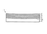
しかしながら、いくつかの実施例では、層厚は、厚みtに対して変動してもよく、式1から逸脱してもよい。これは、広い作動域を持ちうるいわゆる‘チャープ’ミラーを製造する例において有用となりうる。加えて、“デュアル−バンド”ミラー又はダイクロイックミラーなどの多重周期構造体が可能となりうる。そして、これらの構造体は、少なくとも2つの異なる光の波長で反射しうる。“チャープ”ミラーに関し、高反射の波長域は、層の厚みを変えることによって、例えばミラーの垂直方向における層厚を徐々に増加することによって、増大する可能性がある。しかしながら、そのような変動された層厚の使用は、最大反射率を犠牲にしうる。図1は、物理的厚みに関して上記式を維持する高精度光学ミラーを示す。式1を考察することによって、高指数層及び低指数層が相互に異なる厚みを有し、それぞれの屈折率値も異なることに留意すべきである。また、キャリア基板は、重力波干渉計などの大規模な適用例において吸収効果を低減するために透明であってもよい。これらの部材は、典型的には、SiO2、サファイア、Si又はULEを含んでもよい。部材の適切な選択は、ミラーアセンブリの光共振システムへの統合を可能にしうるものであり、ミラーを離間保持するスペーサーに関して類似の又は同じ部材を使用する余地があり、以下の図3の記載も参照可能である。
Claims (15)
- キャリア基板と、
複数の第1タイプ及び第2タイプの交互式結晶性半導体層を含む結晶性スタックであって、第1タイプの層は第2タイプの層よりも高い屈折率を有し、それによりブラッグミラーを形成する結晶性スタックと、を備え、
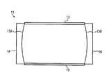
キャリア基板は、0.1mと10mとの間又は1kmと10kmとの間の曲率半径ROCを持って湾曲し、
結晶性スタックは、湾曲したキャリア基板に取り付けられる低吸収結晶性ミラーアセンブリ。 - キャリア基板は透過的であり、とりわけ1064nm又は1550nmの波長において透過的であり、キャリア基板の表面は磨かれている請求項1に記載のミラーアセンブリ。
- キャリア基板は、SiO2、Si、サファイア、又は超低膨張ガラスULEを含む請求項1又は2に記載のミラーアセンブリ。
- ミラーの結晶性半導体層は、AlGaAs三元合金に基づく単結晶エピタキシャル層であり、前記第1タイプ及び第2タイプは、AlxGa1−xAs、ただし0<x<1、を含み、第1タイプの層に関するxは第2タイプの層に関するxよりも小さい請求項1〜3のいずれか一項に記載のミラーアセンブリ。
- 結晶性スタックは、ファンデルワールス力結合及び共有結合のうちの少なくとも一方によって、キャリア基板に取り付けられる請求項1〜4のいずれか一項に記載のミラーアセンブリ。
- 低吸収結晶性ミラーアセンブリの製造方法であって、ミラーは、キャリア基板と、複数の第1タイプ及び第2タイプの交互式結晶性半導体層を含む結晶性スタックであって、第1タイプの層は第2タイプの層よりも高い屈折率を有する結晶性スタックと、を備え、キャリア基板は、0.1mと10mとの間又は5kmと10kmとの間の曲率半径ROCを持って湾曲する製造方法において、
第1の基板を準備するステップと、
キャリア基板を準備するステップと、
例えば分子線エピタキシー法MBEや有機金属気相エピタキシー法MOVPEによって、第1タイプ及び第2タイプの交互式結晶性半導体層の結晶性スタックをエピタキシャルに形成し、それによりブラッグミラーを形成するステップと、
第1の基板からスタックを分離するステップと、
湾曲するキャリア基板にスタックに取り付けるステップとを含む製造方法。 - 第1の基板はGaAs又はGeを含む請求項6に記載の製造方法。
- キャリア基板は透過的であり、とりわけ1064nm又は1550nmの波長において透過的であり、キャリア基板の表面は磨かれている請求項6又は7に記載の製造方法。
- キャリア基板は、SiO2、Si、サファイア、又は超低膨張ガラスULEを含む請求項6〜8のいずれか一項に記載の製造方法。
- 結晶性半導体層は、AlGaAs三元合金に基づく単結晶エピタキシャル層であり、前記第1タイプ及び第2タイプは、AlxGa1−xAs、ただし0<x<1、を含み、第1タイプの層に関するxは第2タイプの層に関するxよりも小さい請求項6〜9のいずれか一項に記載の製造方法。
- 結晶性スタックは、化学−機械的基板除去プロセス又はエピタキシャルリフトオフプロセスを用いることで、第1の基板から分離される請求項6〜10のいずれか一項に記載の製造方法。
- スタックは、ファンデルワールス力結合及び共有結合のうちの少なくとも一方によって、キャリア基板に取り付けられる請求項6〜11のいずれか一項に記載の製造方法。
- スタックはキャリア基板に結合され、当該結合はアニーリングによって強化される請求項12に記載の製造方法。
- 請求項1〜5のいずれか一項に記載の2つのミラーアセンブリを備える光学精密測定用の光共振器であって、ミラーの反射面は所定距離で相互に向かい合い、0.1mから10mのROCに関し、所定の厚みを有するスペーサーが2つのミラーアセンブリの間に存在し、そのスペーサーは2つのミラー間に所定の距離を与える光学精密測定用の光共振器。
- 請求項1〜5のいずれか一項に記載の2つのミラーアセンブリを含む光学精密測定用の光共振器であって、ミラーの反射面は所定距離で相互に向かい合い、1kmから10kmのROCに関し、各ミラーアセンブリは個別に支持される光学精密測定用の光共振器。
Applications Claiming Priority (3)
| Application Number | Priority Date | Filing Date | Title |
|---|---|---|---|
| EP11010091.4 | 2011-12-22 | ||
| EP20110010091 EP2607935B1 (en) | 2011-12-22 | 2011-12-22 | Substrate transferred monocrystalline Bragg mirrors |
| PCT/EP2012/072087 WO2013091986A1 (en) | 2011-12-22 | 2012-11-08 | Substrate transferred monocrystalline bragg mirrors |
Related Child Applications (1)
| Application Number | Title | Priority Date | Filing Date |
|---|---|---|---|
| JP2015124970A Division JP2015207017A (ja) | 2011-12-22 | 2015-06-22 | 基板転移単結晶ブラッグミラー |
Publications (2)
| Publication Number | Publication Date |
|---|---|
| JP2014508317A true JP2014508317A (ja) | 2014-04-03 |
| JP5972284B2 JP5972284B2 (ja) | 2016-08-17 |
Family
ID=47143113
Family Applications (2)
| Application Number | Title | Priority Date | Filing Date |
|---|---|---|---|
| JP2013549852A Expired - Fee Related JP5972284B2 (ja) | 2011-12-22 | 2012-11-08 | 基板転移単結晶ブラッグミラー |
| JP2015124970A Pending JP2015207017A (ja) | 2011-12-22 | 2015-06-22 | 基板転移単結晶ブラッグミラー |
Family Applications After (1)
| Application Number | Title | Priority Date | Filing Date |
|---|---|---|---|
| JP2015124970A Pending JP2015207017A (ja) | 2011-12-22 | 2015-06-22 | 基板転移単結晶ブラッグミラー |
Country Status (5)
| Country | Link |
|---|---|
| US (1) | US9945996B2 (ja) |
| EP (1) | EP2607935B1 (ja) |
| JP (2) | JP5972284B2 (ja) |
| CN (1) | CN103282805B (ja) |
| WO (1) | WO2013091986A1 (ja) |
Families Citing this family (11)
| Publication number | Priority date | Publication date | Assignee | Title |
|---|---|---|---|---|
| JP2016171277A (ja) * | 2015-03-16 | 2016-09-23 | 株式会社東芝 | 半導体発光素子及びその製造方法 |
| US9851528B2 (en) * | 2015-06-05 | 2017-12-26 | Syracuse University | Optical coating permitting cavity self-locking |
| DE102015216655A1 (de) | 2015-09-01 | 2017-03-02 | Trumpf Laser Gmbh | Plattenförmiger laseraktiver Festkörper mit einem kristallinen hochreflektierenden Spiegel und Verfahren zu seiner Herstellung |
| EP3219832B1 (en) * | 2016-03-16 | 2020-06-24 | Thorlabs Inc. | Method for manufacturing direct-bonded optical coatings |
| US10504722B2 (en) | 2017-07-25 | 2019-12-10 | United States Of America As Represented By The Secretary Of The Air Force | Growth of III-nitride semiconductors on thin van der Waals buffers for mechanical lift off and transfer |
| US12352987B2 (en) | 2018-09-11 | 2025-07-08 | Thorlabs, Inc. | Substrate-transferred stacked optical coatings |
| US11365492B2 (en) | 2018-09-11 | 2022-06-21 | Thorlabs, Inc. | Substrate-transferred stacked optical coatings |
| DE102021129829A1 (de) * | 2021-11-16 | 2023-05-17 | Precitec Gmbh & Co. Kg | Ablenkvorrichtung mit beschichtetem Spiegelelement sowie Laserbearbeitungskopf mit derselben |
| EP4239379B1 (en) | 2022-03-01 | 2025-08-27 | Thorlabs, Inc. | Substrate-transferred stacked optical coatings |
| DE102024110479A1 (de) | 2024-04-15 | 2025-10-16 | TRUMPF Lasersystems for Semiconductor Manufacturing SE | Spiegel-Modul, Laser-Vorrichtung und Verfahren zum Herstellen eines Spiegel Moduls |
| WO2025261936A1 (en) * | 2024-06-19 | 2025-12-26 | Asml Netherlands B.V. | Optical element |
Citations (5)
| Publication number | Priority date | Publication date | Assignee | Title |
|---|---|---|---|---|
| JPS62226047A (ja) * | 1986-03-28 | 1987-10-05 | Nippon Telegr & Teleph Corp <Ntt> | 多層膜反射鏡 |
| JPH09180883A (ja) * | 1995-10-27 | 1997-07-11 | Toyota Central Res & Dev Lab Inc | 微小光共振器型有機電界発光素子 |
| JP2006173497A (ja) * | 2004-12-17 | 2006-06-29 | Nikon Corp | 光学素子及びこれを用いた投影露光装置 |
| JP2009088137A (ja) * | 2007-09-28 | 2009-04-23 | Fujinon Corp | 負分散ミラーおよび負分散ミラーを備えたモード同期固体レーザ装置 |
| WO2009062665A2 (en) * | 2007-11-14 | 2009-05-22 | Carl Zeiss Smt Ag | Optical element for the reflection of uv radiation, method for manufacturing the same and projection exposure apparatus comprising the same |
Family Cites Families (9)
| Publication number | Priority date | Publication date | Assignee | Title |
|---|---|---|---|---|
| US4047805A (en) * | 1973-02-14 | 1977-09-13 | Canon Kabushiki Kaisha | Ripple-free dichroic mirrors |
| JPS61281203A (ja) | 1985-06-07 | 1986-12-11 | Toshiba Corp | 低散乱ミラ−及びその製造方法 |
| JPH05346498A (ja) | 1992-06-16 | 1993-12-27 | Nkk Corp | ミラ−装置 |
| JPH08330670A (ja) | 1995-05-29 | 1996-12-13 | Furukawa Electric Co Ltd:The | 半導体レーザ素子の製造方法 |
| US5912915A (en) | 1997-05-19 | 1999-06-15 | Coherent, Inc. | Ultrafast laser with multiply-folded resonant cavity |
| EP2042893A3 (en) | 2007-09-28 | 2010-12-15 | Fujinon Corporation | Negative dispersion mirror and mode-locked solid-state laser apparatus including the mirror |
| JP2011507268A (ja) * | 2007-12-12 | 2011-03-03 | ニューポート コーポレーション | 性能が改善された光学的に被覆された半導体デバイス及び関連した製造方法 |
| US7916395B2 (en) * | 2008-02-26 | 2011-03-29 | Honeywell International Inc. | Cavity ring-down spectroscopy mirror, and methods of using same |
| US20100328762A1 (en) * | 2009-04-27 | 2010-12-30 | Trex Enterprises Corp. | Radiation coating for silicon carbide components |
-
2011
- 2011-12-22 EP EP20110010091 patent/EP2607935B1/en active Active
-
2012
- 2012-11-08 WO PCT/EP2012/072087 patent/WO2013091986A1/en not_active Ceased
- 2012-11-08 JP JP2013549852A patent/JP5972284B2/ja not_active Expired - Fee Related
- 2012-11-08 US US13/825,427 patent/US9945996B2/en active Active
- 2012-11-08 CN CN201280004245.0A patent/CN103282805B/zh not_active Expired - Fee Related
-
2015
- 2015-06-22 JP JP2015124970A patent/JP2015207017A/ja active Pending
Patent Citations (5)
| Publication number | Priority date | Publication date | Assignee | Title |
|---|---|---|---|---|
| JPS62226047A (ja) * | 1986-03-28 | 1987-10-05 | Nippon Telegr & Teleph Corp <Ntt> | 多層膜反射鏡 |
| JPH09180883A (ja) * | 1995-10-27 | 1997-07-11 | Toyota Central Res & Dev Lab Inc | 微小光共振器型有機電界発光素子 |
| JP2006173497A (ja) * | 2004-12-17 | 2006-06-29 | Nikon Corp | 光学素子及びこれを用いた投影露光装置 |
| JP2009088137A (ja) * | 2007-09-28 | 2009-04-23 | Fujinon Corp | 負分散ミラーおよび負分散ミラーを備えたモード同期固体レーザ装置 |
| WO2009062665A2 (en) * | 2007-11-14 | 2009-05-22 | Carl Zeiss Smt Ag | Optical element for the reflection of uv radiation, method for manufacturing the same and projection exposure apparatus comprising the same |
Non-Patent Citations (3)
| Title |
|---|
| JPN7014001332; Garrett D. Cole1, Simon Groblacher, Katharina Gugler, Sylvain Gigan, and Markus Aspelmeyer: 'Monocrystalline AlxGa1-xAs heterostructures for high-reflectivity high-Q micromechanical resonators' APPLIED PHYSICS LETTERS 92,261108, 2008, AMERICAN INSTITUTE OF PHYSI&# * |
| JPN7014001333; Garrett D. Cole1, Yu Bai, Markus Aspelmeyer and Eugene A. Fitzgerald: 'Free-standing AlxGa1-xAs heterostructures by gas-phase etching of germanium' APPLIED PHYSICS LETTERS 96,261102, 2010, AMERICAN INSTITUTE OF PHYSICS * |
| JPN7014001334; Eli Yablonovitch, T. Gmitter, J. P. Harbison and R. Bhat: 'Extreme selectivity in the lift-off of epitaxial GaAs films' APPLIED PHYSICS LETTERS 51(26), 19871228, AMERICAN INSTITUTE OF PHYSICS * |
Also Published As
| Publication number | Publication date |
|---|---|
| CN103282805A (zh) | 2013-09-04 |
| US20140063606A1 (en) | 2014-03-06 |
| JP2015207017A (ja) | 2015-11-19 |
| WO2013091986A1 (en) | 2013-06-27 |
| US9945996B2 (en) | 2018-04-17 |
| EP2607935A1 (en) | 2013-06-26 |
| JP5972284B2 (ja) | 2016-08-17 |
| CN103282805B (zh) | 2016-11-09 |
| EP2607935B1 (en) | 2014-10-29 |
Similar Documents
| Publication | Publication Date | Title |
|---|---|---|
| JP5972284B2 (ja) | 基板転移単結晶ブラッグミラー | |
| US7190524B2 (en) | Process for fabrication of high reflectors by reversal of layer sequence and application thereof | |
| EP2628243B1 (fr) | Structure acoustique heterogene formee a partir d'un materiau homogene | |
| JP2015207017A5 (ja) | ||
| US9337622B2 (en) | Compact distributed bragg reflectors | |
| EP3219832B1 (en) | Method for manufacturing direct-bonded optical coatings | |
| Admassu et al. | Effect of interface grading on the optical performance of distributed Bragg reflector multilayers in Fabry-Pérot optical filters | |
| US11365492B2 (en) | Substrate-transferred stacked optical coatings | |
| CN102053310B (zh) | 基于多重光学Tamm态的多通道滤波器 | |
| EP4239379B1 (en) | Substrate-transferred stacked optical coatings | |
| CN103222136B (zh) | 偏振稳定的表面发射激光二极管 | |
| Kim et al. | AlGaN membrane grating reflector | |
| TWI353097B (en) | Etalon and optoelectronic semiconductor device | |
| US12352987B2 (en) | Substrate-transferred stacked optical coatings | |
| US7812423B2 (en) | Optical device comprising crystalline semiconductor layer and reflective element | |
| Moradinejad et al. | High-Q resonators on double-layer SOI platform | |
| CA3150123A1 (en) | Substrate-transferred stacked optical coatings | |
| CN116770427A (zh) | 基底转移的堆叠光学涂层 | |
| JPH104240A (ja) | 半導体光素子、ウエハ及びその製造方法 | |
| Jasik et al. | Design and fabrication of highly dispersive semiconductor double-chirped mirrors | |
| US11585970B2 (en) | Low loss single crystal multilayer optical component and method of making same | |
| Schenk et al. | Study of (Al, Ga) N Bragg mirrors grown on Al2O3 (0001) and Si (111) by metalorganic vapor phase epitaxy | |
| Sun et al. | Realization of High-Q Microring Resonators with Single Crystal Aluminum Nitride | |
| Hui et al. | Transfer of an AlGaAs/GaAs crystalline Bragg mirror from a GaAs substrate to a fused silica substrate by direct bonding | |
| Wang et al. | Suspended HfO 2 photonic crystal slab on III-nitride/Si platform |
Legal Events
| Date | Code | Title | Description |
|---|---|---|---|
| A131 | Notification of reasons for refusal |
Free format text: JAPANESE INTERMEDIATE CODE: A131 Effective date: 20140501 |
|
| A601 | Written request for extension of time |
Free format text: JAPANESE INTERMEDIATE CODE: A601 Effective date: 20140725 |
|
| A602 | Written permission of extension of time |
Free format text: JAPANESE INTERMEDIATE CODE: A602 Effective date: 20140801 |
|
| A601 | Written request for extension of time |
Free format text: JAPANESE INTERMEDIATE CODE: A601 Effective date: 20140827 |
|
| A602 | Written permission of extension of time |
Free format text: JAPANESE INTERMEDIATE CODE: A602 Effective date: 20140903 |
|
| A601 | Written request for extension of time |
Free format text: JAPANESE INTERMEDIATE CODE: A601 Effective date: 20140926 |
|
| A602 | Written permission of extension of time |
Free format text: JAPANESE INTERMEDIATE CODE: A602 Effective date: 20141003 |
|
| A521 | Request for written amendment filed |
Free format text: JAPANESE INTERMEDIATE CODE: A523 Effective date: 20141016 |
|
| A02 | Decision of refusal |
Free format text: JAPANESE INTERMEDIATE CODE: A02 Effective date: 20150223 |
|
| A711 | Notification of change in applicant |
Free format text: JAPANESE INTERMEDIATE CODE: A711 Effective date: 20150615 |
|
| A521 | Request for written amendment filed |
Free format text: JAPANESE INTERMEDIATE CODE: A523 Effective date: 20150622 |
|
| A521 | Request for written amendment filed |
Free format text: JAPANESE INTERMEDIATE CODE: A821 Effective date: 20150615 |
|
| A911 | Transfer to examiner for re-examination before appeal (zenchi) |
Free format text: JAPANESE INTERMEDIATE CODE: A911 Effective date: 20150714 |
|
| A912 | Re-examination (zenchi) completed and case transferred to appeal board |
Free format text: JAPANESE INTERMEDIATE CODE: A912 Effective date: 20150911 |
|
| A61 | First payment of annual fees (during grant procedure) |
Free format text: JAPANESE INTERMEDIATE CODE: A61 Effective date: 20160712 |
|
| R150 | Certificate of patent or registration of utility model |
Ref document number: 5972284 Country of ref document: JP Free format text: JAPANESE INTERMEDIATE CODE: R150 |
|
| R154 | Certificate of patent or utility model (reissue) |
Free format text: JAPANESE INTERMEDIATE CODE: R154 |
|
| R150 | Certificate of patent or registration of utility model |
Ref document number: 5972284 Country of ref document: JP Free format text: JAPANESE INTERMEDIATE CODE: R150 |
|
| R250 | Receipt of annual fees |
Free format text: JAPANESE INTERMEDIATE CODE: R250 |
|
| R250 | Receipt of annual fees |
Free format text: JAPANESE INTERMEDIATE CODE: R250 |
|
| R250 | Receipt of annual fees |
Free format text: JAPANESE INTERMEDIATE CODE: R250 |
|
| R250 | Receipt of annual fees |
Free format text: JAPANESE INTERMEDIATE CODE: R250 |
|
| LAPS | Cancellation because of no payment of annual fees |