JP2014503129A - Solar cell and manufacturing method thereof - Google Patents
Solar cell and manufacturing method thereof Download PDFInfo
- Publication number
- JP2014503129A JP2014503129A JP2013550374A JP2013550374A JP2014503129A JP 2014503129 A JP2014503129 A JP 2014503129A JP 2013550374 A JP2013550374 A JP 2013550374A JP 2013550374 A JP2013550374 A JP 2013550374A JP 2014503129 A JP2014503129 A JP 2014503129A
- Authority
- JP
- Japan
- Prior art keywords
- layer
- solar cell
- support substrate
- reflective layer
- back electrode
- Prior art date
- Legal status (The legal status is an assumption and is not a legal conclusion. Google has not performed a legal analysis and makes no representation as to the accuracy of the status listed.)
- Pending
Links
- 238000004519 manufacturing process Methods 0.000 title claims description 16
- 239000000758 substrate Substances 0.000 claims abstract description 37
- 230000031700 light absorption Effects 0.000 claims abstract description 25
- 239000000463 material Substances 0.000 claims abstract description 10
- 238000000034 method Methods 0.000 claims description 21
- 238000007254 oxidation reaction Methods 0.000 claims description 12
- 229910052751 metal Inorganic materials 0.000 claims description 11
- 239000002184 metal Substances 0.000 claims description 11
- 229910052782 aluminium Inorganic materials 0.000 claims description 8
- XAGFODPZIPBFFR-UHFFFAOYSA-N aluminium Chemical compound [Al] XAGFODPZIPBFFR-UHFFFAOYSA-N 0.000 claims description 8
- 239000011777 magnesium Substances 0.000 claims description 8
- 239000010936 titanium Substances 0.000 claims description 8
- MCMNRKCIXSYSNV-UHFFFAOYSA-N Zirconium dioxide Chemical compound O=[Zr]=O MCMNRKCIXSYSNV-UHFFFAOYSA-N 0.000 claims description 6
- FYYHWMGAXLPEAU-UHFFFAOYSA-N Magnesium Chemical compound [Mg] FYYHWMGAXLPEAU-UHFFFAOYSA-N 0.000 claims description 4
- 238000004070 electrodeposition Methods 0.000 claims description 4
- 229910052749 magnesium Inorganic materials 0.000 claims description 4
- WFKWXMTUELFFGS-UHFFFAOYSA-N tungsten Chemical compound [W] WFKWXMTUELFFGS-UHFFFAOYSA-N 0.000 claims description 4
- 229910052721 tungsten Inorganic materials 0.000 claims description 4
- 239000010937 tungsten Substances 0.000 claims description 4
- RTAQQCXQSZGOHL-UHFFFAOYSA-N Titanium Chemical compound [Ti] RTAQQCXQSZGOHL-UHFFFAOYSA-N 0.000 claims description 3
- 229910052790 beryllium Inorganic materials 0.000 claims description 3
- ATBAMAFKBVZNFJ-UHFFFAOYSA-N beryllium atom Chemical compound [Be] ATBAMAFKBVZNFJ-UHFFFAOYSA-N 0.000 claims description 3
- 229910052759 nickel Inorganic materials 0.000 claims description 3
- 230000001590 oxidative effect Effects 0.000 claims description 3
- 229910052715 tantalum Inorganic materials 0.000 claims description 3
- GUVRBAGPIYLISA-UHFFFAOYSA-N tantalum atom Chemical compound [Ta] GUVRBAGPIYLISA-UHFFFAOYSA-N 0.000 claims description 3
- 229910052719 titanium Inorganic materials 0.000 claims description 3
- 229910052804 chromium Inorganic materials 0.000 claims description 2
- 239000003792 electrolyte Substances 0.000 claims description 2
- 229910052742 iron Inorganic materials 0.000 claims description 2
- 239000007769 metal material Substances 0.000 claims 1
- 230000003647 oxidation Effects 0.000 description 10
- 229910052733 gallium Inorganic materials 0.000 description 7
- XLOMVQKBTHCTTD-UHFFFAOYSA-N Zinc monoxide Chemical compound [Zn]=O XLOMVQKBTHCTTD-UHFFFAOYSA-N 0.000 description 6
- 238000006243 chemical reaction Methods 0.000 description 6
- 239000010949 copper Substances 0.000 description 6
- 150000002500 ions Chemical class 0.000 description 6
- GYHNNYVSQQEPJS-UHFFFAOYSA-N Gallium Chemical compound [Ga] GYHNNYVSQQEPJS-UHFFFAOYSA-N 0.000 description 5
- 150000001875 compounds Chemical class 0.000 description 5
- 229910052738 indium Inorganic materials 0.000 description 5
- 239000011669 selenium Substances 0.000 description 5
- VYPSYNLAJGMNEJ-UHFFFAOYSA-N Silicium dioxide Chemical compound O=[Si]=O VYPSYNLAJGMNEJ-UHFFFAOYSA-N 0.000 description 4
- 229910052980 cadmium sulfide Inorganic materials 0.000 description 4
- 230000000694 effects Effects 0.000 description 4
- 239000010408 film Substances 0.000 description 4
- PXHVJJICTQNCMI-UHFFFAOYSA-N nickel Substances [Ni] PXHVJJICTQNCMI-UHFFFAOYSA-N 0.000 description 4
- 239000004065 semiconductor Substances 0.000 description 4
- 229910052814 silicon oxide Inorganic materials 0.000 description 4
- 238000004544 sputter deposition Methods 0.000 description 4
- RYGMFSIKBFXOCR-UHFFFAOYSA-N Copper Chemical compound [Cu] RYGMFSIKBFXOCR-UHFFFAOYSA-N 0.000 description 3
- ZOKXTWBITQBERF-UHFFFAOYSA-N Molybdenum Chemical compound [Mo] ZOKXTWBITQBERF-UHFFFAOYSA-N 0.000 description 3
- KTSFMFGEAAANTF-UHFFFAOYSA-N [Cu].[Se].[Se].[In] Chemical compound [Cu].[Se].[Se].[In] KTSFMFGEAAANTF-UHFFFAOYSA-N 0.000 description 3
- 239000011651 chromium Substances 0.000 description 3
- 229910052802 copper Inorganic materials 0.000 description 3
- APFVFJFRJDLVQX-UHFFFAOYSA-N indium atom Chemical compound [In] APFVFJFRJDLVQX-UHFFFAOYSA-N 0.000 description 3
- 238000012986 modification Methods 0.000 description 3
- 230000004048 modification Effects 0.000 description 3
- 229910052750 molybdenum Inorganic materials 0.000 description 3
- 239000011733 molybdenum Substances 0.000 description 3
- 239000002243 precursor Substances 0.000 description 3
- 239000011787 zinc oxide Substances 0.000 description 3
- 229910018072 Al 2 O 3 Inorganic materials 0.000 description 2
- BUGBHKTXTAQXES-UHFFFAOYSA-N Selenium Chemical compound [Se] BUGBHKTXTAQXES-UHFFFAOYSA-N 0.000 description 2
- 238000000224 chemical solution deposition Methods 0.000 description 2
- 239000013078 crystal Substances 0.000 description 2
- 238000000151 deposition Methods 0.000 description 2
- 238000009792 diffusion process Methods 0.000 description 2
- 239000011521 glass Substances 0.000 description 2
- 239000010931 gold Substances 0.000 description 2
- 239000010410 layer Substances 0.000 description 2
- 239000012528 membrane Substances 0.000 description 2
- 238000005240 physical vapour deposition Methods 0.000 description 2
- 238000010248 power generation Methods 0.000 description 2
- 229910052711 selenium Inorganic materials 0.000 description 2
- 239000010409 thin film Substances 0.000 description 2
- WUPHOULIZUERAE-UHFFFAOYSA-N 3-(oxolan-2-yl)propanoic acid Chemical compound OC(=O)CCC1CCCO1 WUPHOULIZUERAE-UHFFFAOYSA-N 0.000 description 1
- VYZAMTAEIAYCRO-UHFFFAOYSA-N Chromium Chemical compound [Cr] VYZAMTAEIAYCRO-UHFFFAOYSA-N 0.000 description 1
- 229910052779 Neodymium Inorganic materials 0.000 description 1
- NINIDFKCEFEMDL-UHFFFAOYSA-N Sulfur Chemical compound [S] NINIDFKCEFEMDL-UHFFFAOYSA-N 0.000 description 1
- 238000010521 absorption reaction Methods 0.000 description 1
- PNEYBMLMFCGWSK-UHFFFAOYSA-N aluminium oxide Inorganic materials [O-2].[O-2].[O-2].[Al+3].[Al+3] PNEYBMLMFCGWSK-UHFFFAOYSA-N 0.000 description 1
- 230000015572 biosynthetic process Effects 0.000 description 1
- YNLHHZNOLUDEKQ-UHFFFAOYSA-N copper;selanylidenegallium Chemical compound [Cu].[Se]=[Ga] YNLHHZNOLUDEKQ-UHFFFAOYSA-N 0.000 description 1
- 230000002542 deteriorative effect Effects 0.000 description 1
- 238000001704 evaporation Methods 0.000 description 1
- PCHJSUWPFVWCPO-UHFFFAOYSA-N gold Chemical compound [Au] PCHJSUWPFVWCPO-UHFFFAOYSA-N 0.000 description 1
- 229910052737 gold Inorganic materials 0.000 description 1
- 238000010438 heat treatment Methods 0.000 description 1
- 239000012535 impurity Substances 0.000 description 1
- AMGQUBHHOARCQH-UHFFFAOYSA-N indium;oxotin Chemical compound [In].[Sn]=O AMGQUBHHOARCQH-UHFFFAOYSA-N 0.000 description 1
- 239000012212 insulator Substances 0.000 description 1
- XEEYBQQBJWHFJM-UHFFFAOYSA-N iron Substances [Fe] XEEYBQQBJWHFJM-UHFFFAOYSA-N 0.000 description 1
- 229910021645 metal ion Inorganic materials 0.000 description 1
- 150000002739 metals Chemical class 0.000 description 1
- QEFYFXOXNSNQGX-UHFFFAOYSA-N neodymium atom Chemical compound [Nd] QEFYFXOXNSNQGX-UHFFFAOYSA-N 0.000 description 1
- 238000007747 plating Methods 0.000 description 1
- 238000011160 research Methods 0.000 description 1
- 239000000126 substance Substances 0.000 description 1
- 229910052717 sulfur Inorganic materials 0.000 description 1
- 239000011593 sulfur Substances 0.000 description 1
- XOLBLPGZBRYERU-UHFFFAOYSA-N tin dioxide Chemical compound O=[Sn]=O XOLBLPGZBRYERU-UHFFFAOYSA-N 0.000 description 1
- 229910001887 tin oxide Inorganic materials 0.000 description 1
- 238000001771 vacuum deposition Methods 0.000 description 1
- YVTHLONGBIQYBO-UHFFFAOYSA-N zinc indium(3+) oxygen(2-) Chemical compound [O--].[Zn++].[In+3] YVTHLONGBIQYBO-UHFFFAOYSA-N 0.000 description 1
Images
Classifications
-
- H—ELECTRICITY
- H01—ELECTRIC ELEMENTS
- H01L—SEMICONDUCTOR DEVICES NOT COVERED BY CLASS H10
- H01L31/00—Semiconductor devices sensitive to infrared radiation, light, electromagnetic radiation of shorter wavelength or corpuscular radiation and specially adapted either for the conversion of the energy of such radiation into electrical energy or for the control of electrical energy by such radiation; Processes or apparatus specially adapted for the manufacture or treatment thereof or of parts thereof; Details thereof
- H01L31/04—Semiconductor devices sensitive to infrared radiation, light, electromagnetic radiation of shorter wavelength or corpuscular radiation and specially adapted either for the conversion of the energy of such radiation into electrical energy or for the control of electrical energy by such radiation; Processes or apparatus specially adapted for the manufacture or treatment thereof or of parts thereof; Details thereof adapted as photovoltaic [PV] conversion devices
- H01L31/054—Optical elements directly associated or integrated with the PV cell, e.g. light-reflecting means or light-concentrating means
-
- H—ELECTRICITY
- H01—ELECTRIC ELEMENTS
- H01L—SEMICONDUCTOR DEVICES NOT COVERED BY CLASS H10
- H01L31/00—Semiconductor devices sensitive to infrared radiation, light, electromagnetic radiation of shorter wavelength or corpuscular radiation and specially adapted either for the conversion of the energy of such radiation into electrical energy or for the control of electrical energy by such radiation; Processes or apparatus specially adapted for the manufacture or treatment thereof or of parts thereof; Details thereof
- H01L31/18—Processes or apparatus specially adapted for the manufacture or treatment of these devices or of parts thereof
-
- Y—GENERAL TAGGING OF NEW TECHNOLOGICAL DEVELOPMENTS; GENERAL TAGGING OF CROSS-SECTIONAL TECHNOLOGIES SPANNING OVER SEVERAL SECTIONS OF THE IPC; TECHNICAL SUBJECTS COVERED BY FORMER USPC CROSS-REFERENCE ART COLLECTIONS [XRACs] AND DIGESTS
- Y02—TECHNOLOGIES OR APPLICATIONS FOR MITIGATION OR ADAPTATION AGAINST CLIMATE CHANGE
- Y02E—REDUCTION OF GREENHOUSE GAS [GHG] EMISSIONS, RELATED TO ENERGY GENERATION, TRANSMISSION OR DISTRIBUTION
- Y02E10/00—Energy generation through renewable energy sources
- Y02E10/50—Photovoltaic [PV] energy
- Y02E10/52—PV systems with concentrators
Abstract
本発明による太陽電池は、支持基板と、前記支持基板上の反射層と、前記反射層上に配置され、前記反射層と同一の物質を含む酸化層と、前記酸化層上の裏面電極層と、前記裏面電極層上の光吸収層と、前記光吸収層上のバッファ層と、前記バッファ層上のウィンドウ層とを含む。
【選択図】図1The solar cell according to the present invention includes a support substrate, a reflective layer on the support substrate, an oxide layer disposed on the reflective layer and including the same material as the reflective layer, and a back electrode layer on the oxide layer. A light absorption layer on the back electrode layer, a buffer layer on the light absorption layer, and a window layer on the buffer layer.
[Selection] Figure 1
Description
開示の実施形態は、太陽電池及びその製造方法に関する。 The disclosed embodiments relate to a solar cell and a method for manufacturing the solar cell.
最近、エネルギーの需要が増加するにつれて、太陽光エネルギーを電気エネルギーに変換させる太陽光発電に関する開発が進められている。 Recently, as the demand for energy increases, development related to solar power generation that converts solar energy into electric energy has been promoted.
特に、ガラス基板、金属後面電極層、p型CIGS系光吸収部、バッファ層、n型透明電極層などを含む支持基板構造のpnヘテロ接合装置であるCIGS系太陽電池が広く使われている。また、このような太陽電池の効率を増加するため、様々な研究が進行しつつある。 In particular, CIGS solar cells, which are pn heterojunction devices having a supporting substrate structure including a glass substrate, a metal back electrode layer, a p-type CIGS light absorbing portion, a buffer layer, an n-type transparent electrode layer, and the like, are widely used. In addition, various researches are in progress to increase the efficiency of such solar cells.
開示の実施形態は、向上した光電変換効率を有する太陽電池及びその製造方法を提供するものである。 Embodiments of the disclosure provide a solar cell having improved photoelectric conversion efficiency and a method for manufacturing the solar cell.
本発明による太陽電池は、支持基板と、前記支持基板上の反射層と、前記反射層上に配置され、前記反射層と同一の物質を含む酸化層と、前記酸化層上の裏面電極層と、前記裏面電極層上の光吸収層と、前記光吸収層上のバッファ層と、及び前記バッファ層上のウィンドウ層とを含む。 The solar cell according to the present invention includes a support substrate, a reflective layer on the support substrate, an oxide layer disposed on the reflective layer and including the same material as the reflective layer, and a back electrode layer on the oxide layer. A light absorption layer on the back electrode layer, a buffer layer on the light absorption layer, and a window layer on the buffer layer.
本発明による太陽電池の製造方法は、金属を含む支持基板上に反射層を形成するステップと、前記反射層の上部を酸化して酸化層を形成するステップと、前記酸化層上に裏面電極層を形成するステップと、前記裏面電極層上に光吸収層を形成するステップと、前記光吸収層上にバッファ層を形成するステップと、前記バッファ層上にウィンドウ層を形成するステップとを含む。 The method for manufacturing a solar cell according to the present invention includes a step of forming a reflective layer on a support substrate containing metal, a step of oxidizing an upper part of the reflective layer to form an oxide layer, and a back electrode layer on the oxide layer. Forming a light absorption layer on the back electrode layer, forming a buffer layer on the light absorption layer, and forming a window layer on the buffer layer.
本発明によると、支持基板上に反射層を形成し、前記反射層の上面を酸化して、酸化層を形成する。これにより、信頼性が向上し、向上した光電変換効率を有する太陽電池を提供することができる。 According to the present invention, the reflective layer is formed on the support substrate, and the upper surface of the reflective layer is oxidized to form the oxidized layer. Thereby, reliability improves and the solar cell which has the improved photoelectric conversion efficiency can be provided.
本発明を説明するに当たって、各支持基板、層、膜、または電極などが、各基板、層、膜、または電極などの“上(on)”に、または“下(under)”に形成されることと記載される場合において、“上(on)”と“下(under)”は、“直接(directly)”または“他の構成要素を介して(indirectly)”形成されることを全て含む。また、各構成要素の上または下に対する基準は、図面を基準として説明する。図面において、各構成要素のサイズは説明のために誇張することがあり、実際に適用されるサイズを意味するものではない。 In describing the present invention, each support substrate, layer, membrane, or electrode or the like is formed “on” or “under” each substrate, layer, membrane, or electrode, or the like. Where “on” and “under” include all being “directly” or “indirectly” formed. Further, the reference to the top or bottom of each component will be described with reference to the drawings. In the drawings, the size of each component may be exaggerated for the purpose of explanation, and does not mean a size that is actually applied.
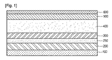
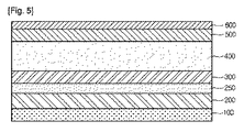
図1は、本発明の実施形態による太陽電池の断面図である。図1を参照すると、実施形態による太陽電池は、支持基板100と、前記支持基板100上の反射層200と、前記反射層200上の酸化層250と、前記酸化層250上の裏面電極層300(後面電極層)と、前記裏面電極層300上の光吸収層400と、前記光吸収層400上のバッファ層500と、前記バッファ層500上のウィンドウ層600とを含む。
FIG. 1 is a cross-sectional view of a solar cell according to an embodiment of the present invention. Referring to FIG. 1, the solar cell according to the embodiment includes a
前記支持基板100は、プレート状を有し、前記反射層200と、酸化層250と、裏面電極層300と、光吸収層400と、バッファ層500と、ウィンドウ層600とを支持する。
The
前記支持基板100は、絶縁体であるか、前記支持基板100は、透明であるか、また、前記支持基板100は、リジッドであるか、フレキシブルである。
The
前記支持基板100は、金属(metal)を含んで形成される。より詳しくは、前記支持基板100は、Fe、Ni、Crなどの物質を含んで形成され得る。前記支持基板100は、透明であるか、リジッドであるか、フレキシブルである。
The
前記支持基板100が金属を含んで形成される場合、ガラスを含む支持基板に比べて、生産コストが節減されて、経済性の点で有利であるか、フレキシブルであって、可搬性の点で有利である。
When the
しかし、金属を含む支持基板100を形成する場合、前記支持基板100に含まれた金属イオンが上部層に拡散されることがあり、これにより、太陽電池の電気的特性が悪化するなどの問題点が発生し得る。
However, when forming the
したがって、酸化層250を形成することにより、支持基板100に含まれたイオンが上部に拡散することを防止することができる。すなわち、前記酸化層250は、拡散防止層として働くことができる。
Therefore, by forming the
また、光吸収層400を通って支持基板100に入射する光が、前記反射層200により、前記光吸収層400に再反射することがあるので、光電変換効率を向上させることができる。
In addition, light incident on the
このような反射層としては、シリコンオキサイド(SiOx)、または、アルミニウム(Al2O3)などの物質、又は、異種接合層が使用され得る。 As such a reflective layer, a material such as silicon oxide (SiOx) or aluminum (Al 2 O 3 ), or a heterogeneous bonding layer can be used.
前記反射層200として、Ti/SiOxなどの異種接合層が使用される場合、Tiを蒸着した後、SiOxなどの物質を蒸着するので、工程が増加して、生産性の面で改善の余地がある。
When a heterogeneous bonding layer such as Ti / SiOx is used as the
本発明の実施形態では、支持基板100上に反射層200を形成し、前記反射層200を酸化させて酸化層250を形成するので、工程の便宜性が増大する。
In the embodiment of the present invention, since the
前記反射層200は、酸化膜を形成することのできる物質を使用し、例えば、タンタル(Ta)、タングステン(W)、アルミニウム(Al)、マグネシウム(Mg)、ネオジウム、ジルコニア、ベリリウム(Be)、チタン(Ti)などの物質を使用することができる。
The
前記反射層200は、光吸収層400を通って支持基板100の方向に入射する光を、光吸収層400へ反射して、太陽電池の光電変換効率を増加させる。
The
前記反射層200の厚さが10nm以下であると、前記光吸収層400を通った光の反射効率が減少し、5000nm以上であると、素子の小型化を具現しにくいので、このような点を考えて、10nm乃至5000nmの厚さで形成するのが望ましい。
If the thickness of the
前記酸化処理により、前記反射層200の厚さは、初期厚さに比べて減少する。また、前記酸化処理後の反射層200及び酸化層250の厚さを合わせた値は、前記酸化処理前の反射層200の厚さよりも大きい値を有することがある。
Due to the oxidation treatment, the thickness of the
前記酸化層250は、前記支持基板100に含まれるイオンの、高温での経路を長くし、また、共有結合及びイオン結合をなしている酸化層250の特性上、前記支持基板100に含まれるイオンが、裏面電極層300以上の上部に拡散することを防止することができる。
The
前記酸化処理により形成される酸化層250の厚さが、前記反射層200の初期厚さの5%以下に形成されると、前記支持基板100に含まれるイオンが、裏面電極層300以上の上部に拡散することを防止する効果が不十分であり、前記反射層200の初期厚さの80%以上に形成されると、前記反射層200の反射効果が減少することがあるので、これを考えて、前記酸化層250の厚さは、前記反射層200の初期厚さの5%乃至80%の範囲で形成することが望ましい。
When the thickness of the
前記酸化層250の上には、裏面電極層300が形成される。前記裏面電極層300は、導電層である。前記裏面電極層300は、太陽電池のうち、前記光吸収層400で生成された電荷が移動するようにして、太陽電池の外部に電流を流すようにすることができる。前記裏面電極層300は、このような機能を果たすために、電気伝導度が高く、比抵抗が小さくなければならない。
A
また、前記裏面電極層300は、CIGS化合物の形成の際に伴う硫黄(S)、または、セレニウム(Se)の雰囲気下での熱処理時、高温安定性が維持されなければならない。
The
このような裏面電極層300は、モリブデン(Mo)、ニッケル(Ni)、金(Au)、アルミニウム(Al)、クロム(Cr)、タングステン(W)、及び銅(Cu)のいずれかで形成される。このうち、特に、モリブデン(Mo)は、上述した裏面電極層300に要求される特性を全般的に満たすことができる。
Such a
前記裏面電極層300は、2以上の層を含むことができる。この場合、それぞれの層は、同一の金属で形成されるか、互いに異なる金属で形成される。
The
前記裏面電極層300の上には、光吸収層400が形成される。前記光吸収層400は、p型半導体化合物を含む。より詳しくは、前記光吸収層400は、I−III−VI族係化合物を含む。例えば、前記光吸収層400は、銅−インジウム−ガリウム−セレナイド系(Cu(In,Ga)Se2;CIGS系)結晶構造、銅−インジウム−セレナイド系、または、銅−ガリウム−セレナイド系結晶を有することができる。前記光吸収層400のエネルギーバンドギャップ(band gap)は、約1eV乃至1.8eVである。
A
前記光吸収層400の上には、バッファ層500が形成される。本実施形態のように、CIGS化合物を光吸収層400として有する太陽電池は、p型半導体であるCIGS化合物薄膜と、n型半導体であるウィンドウ層600とがpn接合を形成する。しかし、2つの物質は、格子定数とバンドギャップエネルギーの差が大きいため、良好な接合を形成するためには、バンドギャップが、2つの物質の中間に位置するバッファ層が必要である。
A
前記バッファ層500を形成する物質としては、CdS、ZnSなどがあるが、太陽電池の発電効率の面で、CdSが相対的に優れている。CdS薄膜は、n型半導体であり、インジウム(In)、ガリウム(Ga)、アルミニウム(Al)などをドーピングすることで、低い抵抗値を得ることができる。
Examples of the material forming the
前記バッファ層500の上には、ウィンドウ層600が形成される。前記ウィンドウ層600は、透明であり、導電層として働くことができる。前記ウィンドウ層600は、酸化物を含む。例えば、前記ウィンドウ層600は、酸化亜鉛(zinc oxide)、インジウムスズ酸化物(indium tin oxide;ITO)、または、インジウム亜鉛酸化物(indium zinc oxide;IZO)などを含むことができる。
A
また、前記酸化物は、アルミニウム(Al)、アルミナ(Al2O3)、マグネシウム(Mg)、または、ガリウム(Ga)などの導電性不純物を含むことができる。より詳しくは、前記ウィンドウ層600は、アルミニウムがドーピングされた酸化亜鉛(Al doped zinc oxide;AZO)、または、ガリウムがドーピングされた酸化亜鉛(Ga doped zinc oxide;GZO)などを含むことができる。
The oxide may include a conductive impurity such as aluminum (Al), alumina (Al 2 O 3 ), magnesium (Mg), or gallium (Ga). More specifically, the
以上で検討したように、本発明の実施形態によれば、反射層200により、向上した光電換効率を有する。
As discussed above, according to the embodiment of the present invention, the
また、酸化層250により、支持基板100に含まれたイオンが上層に拡散することを防止して、信頼性の向上した太陽電池を提供することができる。
In addition, the
また、前記酸化層250は、反射層200の上部に酸化処理を施して形成されることで、工程の便宜性が増大し、生産性が向上される。
In addition, the
図2乃至図5は、本発明の施形態による太陽電池の製造方法を示す断面図である。 2 to 5 are cross-sectional views illustrating a method for manufacturing a solar cell according to an embodiment of the present invention.
本実施形態の製造方法に関する説明は、前述した太陽電池に関する説明を参考する。前述した太陽電池に関する説明は、本実施形態の製造方法に関する説明に、本質的に組み合わせることができる。 The description regarding the manufacturing method of this embodiment refers to the description regarding the solar cell mentioned above. The description regarding the solar cell described above can be essentially combined with the description regarding the manufacturing method of the present embodiment.
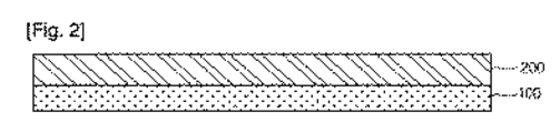
図2に示しているように、支持基板100の上に反射層200が形成される。
As shown in FIG. 2, the
前記反射層200は、スパッタリング(Sputtering)法、または、真空蒸着(Vacuum Evaporation)法で形成することができる。
The
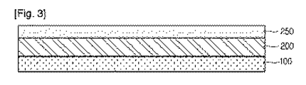
図3を参照すると、前記反射層200の上に酸化層250が形成される。前記酸化層250は、前記反射層200の上部を酸化処理して形成することができる。すなわち、前記酸化層250は、前記反射層200の酸化物として形成され得る。
Referring to FIG. 3, an
前記酸化処理は、PEO(plasma-electrolyte oxidization)、または、電着(ED:electro deposition)の方法を用いることができる。 For the oxidation treatment, PEO (plasma-electrolyte oxidization) or electrodeposition (ED: electro deposition) can be used.
前記酸化処理により形成される前記酸化層250の厚さは、前記反射層200の厚さの5%乃至80%範囲で形成することができる。
The thickness of the
また、前記酸化処理後の反射層200と酸化層250との厚さを合わせた値は、酸化処理前の反射層200の厚さよりも大きい値を有することがある。
In addition, the combined thickness of the
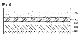
図4を参照すると、前記酸化層250の上に裏面電極層300が形成される。前記裏面電極層300は、モリブデンを用いて、PVD(Physical Vapor Deposition)、または、メッキの方法で形成される。
Referring to FIG. 4, a
ついで、前記裏面電極層300の上に光吸収層400が形成される。前記光吸収層400は、例えば、銅、インジウム、ガリウム、セレニウムを、同時又は別々に蒸発させながら、銅−インジウム−ガリウム−セレナイド系(Cu(In,Ga)Se2;CIGS系)の光吸収層400を形成する方法と、金属プリカーサ膜を形成させた後、セレン化(selenization)工程により形成させる方法とが幅広く使われている。
Next, a
金属プリカーサ膜を形成させた後、セレン化することを詳述すると、銅ターゲット、インジウムターゲット、ガリウムターゲットを使用するスパッタリング工程により、前記裏面電極層300の上に金属プリカーサ膜が形成される。
More specifically, after forming the metal precursor film, selenization is performed. The metal precursor film is formed on the
図5を参照すると、前記光吸収層400の上にバッファ層500が形成される。前記バッファ層500は、硫化カドミウムが、スパッタリング工程、または、溶液成長法(chemical bath deposition;CBD)などにより蒸着されて形成される。
Referring to FIG. 5, a
ついで、前記バッファ層500の上にウィンドウ層600が形成される。前記ウィンドウ層600は、CVD工程、または、スパッタリング工程により蒸着されて形成される。
Then, a
このように、本発明の実施形態によると、反射層200により、向上した光電変換効率を有する太陽電池を提供することができる。
Thus, according to the embodiment of the present invention, the
また、酸化層250により、支持基板100に含まれたイオンが上層に拡散することを防止して、信頼性の向上した太陽電池を提供することができる。
In addition, the
更に、前記反射層200の上に酸化処理を施すことで、工程の便宜性が増大して、生産性が向上される。
Furthermore, by performing an oxidation treatment on the
以上、実施形態に説明された特徴、構造、効果などは、本発明の少なくとも1つの実施形態に含まれ、必ず1つの実施形態のみに限定されるものではない。延いては、各実施形態で例示された特徴、構造、効果などは、実施形態が属する分野の通常の知識を有する者により他の実施形態に対しても組合または変形されて実施可能である。したがって、このような組合と変形に関連した内容は、本発明の範囲に含まれることと解釈されるべきである。 As described above, the features, structures, effects, and the like described in the embodiments are included in at least one embodiment of the present invention, and are not necessarily limited to only one embodiment. As a result, the features, structures, effects, and the like exemplified in each embodiment can be combined or modified with respect to other embodiments by a person having ordinary knowledge in the field to which the embodiment belongs. Accordingly, contents related to such combinations and modifications should be construed as being included in the scope of the present invention.
以上、本発明を好ましい実施形態をもとに説明したが、これは単なる例示であり、本発明を限定するものではなく、本発明が属する分野の通常の知識を有する者であれば、本発明の本質的な特性を逸脱しない範囲内で、多様な変形及び応用が可能であることが分かるであろう。例えば、実施形態に具体的に表れた各構成要素は変形して実施することができる。そして、このような変形及び応用にかかわる差異点は、添付の特許請求の範囲で規定する本発明の範囲に含まれるものと解釈されるべきである。 The present invention has been described based on the preferred embodiments. However, this is merely an example, and is not intended to limit the present invention. Any person having ordinary knowledge in the field to which the present invention belongs can be used. It will be understood that various modifications and applications are possible without departing from the essential characteristics of the present invention. For example, each component specifically shown in the embodiment can be implemented by being modified. Such differences in modification and application should be construed as being included in the scope of the present invention as defined in the appended claims.
Claims (10)
前記支持基板上の反射層と、
前記反射層上に配置され、前記反射層と同一の物質を含む酸化層と、
前記酸化層上の裏面電極層と、
前記裏面電極層上の光吸収層と、
前記光吸収層上のバッファ層と、
前記バッファ層上のウィンドウ層とを含むことを特徴とする太陽電池。 A support substrate;
A reflective layer on the support substrate;
An oxide layer disposed on the reflective layer and including the same material as the reflective layer;
A back electrode layer on the oxide layer;
A light absorbing layer on the back electrode layer;
A buffer layer on the light absorbing layer;
And a window layer on the buffer layer.
前記反射層の上部を酸化させて酸化層を形成するステップと、
前記酸化層の上に裏面電極層を形成するステップと、
前記裏面電極層の上に光吸収層を形成するステップと、
前記光吸収層の上にバッファ層を形成するステップと、
前記バッファ層の上にウィンドウ層を形成するステップとを含むことを特徴とする太陽電池の製造方法。 Forming a reflective layer on a support substrate comprising a metal;
Oxidizing the upper part of the reflective layer to form an oxide layer;
Forming a back electrode layer on the oxide layer;
Forming a light absorption layer on the back electrode layer;
Forming a buffer layer on the light absorbing layer;
Forming a window layer on the buffer layer. A method for manufacturing a solar cell, comprising:
Applications Claiming Priority (3)
| Application Number | Priority Date | Filing Date | Title |
|---|---|---|---|
| KR10-2011-0007514 | 2011-01-25 | ||
| KR1020110007514A KR101134730B1 (en) | 2011-01-25 | 2011-01-25 | Solar cell apparatus and method of fabricating the same |
| PCT/KR2011/007404 WO2012102454A1 (en) | 2011-01-25 | 2011-10-06 | Solar cell and method for manufacturing the same |
Publications (1)
| Publication Number | Publication Date |
|---|---|
| JP2014503129A true JP2014503129A (en) | 2014-02-06 |
Family
ID=46143452
Family Applications (1)
| Application Number | Title | Priority Date | Filing Date |
|---|---|---|---|
| JP2013550374A Pending JP2014503129A (en) | 2011-01-25 | 2011-10-06 | Solar cell and manufacturing method thereof |
Country Status (5)
| Country | Link |
|---|---|
| EP (1) | EP2534704A1 (en) |
| JP (1) | JP2014503129A (en) |
| KR (1) | KR101134730B1 (en) |
| CN (1) | CN102959735B (en) |
| WO (1) | WO2012102454A1 (en) |
Families Citing this family (2)
| Publication number | Priority date | Publication date | Assignee | Title |
|---|---|---|---|---|
| KR101634075B1 (en) * | 2014-12-19 | 2016-06-28 | 주식회사 포스코 | Solar cell |
| US20220238747A1 (en) | 2021-01-28 | 2022-07-28 | Solaero Technologies Corp. | Inverted metamorphic multijunction solar cell |
Family Cites Families (8)
| Publication number | Priority date | Publication date | Assignee | Title |
|---|---|---|---|---|
| SE0301350D0 (en) * | 2003-05-08 | 2003-05-08 | Forskarpatent I Uppsala Ab | A thin-film solar cell |
| US7629661B2 (en) | 2006-02-10 | 2009-12-08 | Noble Peak Vision Corp. | Semiconductor devices with photoresponsive components and metal silicide light blocking structures |
| US20080295884A1 (en) * | 2007-05-29 | 2008-12-04 | Sharma Pramod K | Method of making a photovoltaic device or front substrate with barrier layer for use in same and resulting product |
| JP4974986B2 (en) | 2007-09-28 | 2012-07-11 | 富士フイルム株式会社 | Solar cell substrate and solar cell |
| KR101372536B1 (en) * | 2007-10-02 | 2014-03-18 | 엘지전자 주식회사 | Tandem Thin Film Solar Cell And Fabrication Method Thereof |
| ES2422256T3 (en) * | 2007-11-09 | 2013-09-10 | Sunpreme Inc | Low cost solar cells and methods for their production |
| US20100139753A1 (en) * | 2008-12-05 | 2010-06-10 | Applied Materials, Inc. | Semiconductor device and method of producing a semiconductor device |
| KR20100073717A (en) * | 2008-12-23 | 2010-07-01 | 삼성전자주식회사 | Solar cell and method of fabricating the same |
-
2011
- 2011-01-25 KR KR1020110007514A patent/KR101134730B1/en not_active IP Right Cessation
- 2011-10-06 EP EP11856637A patent/EP2534704A1/en not_active Withdrawn
- 2011-10-06 WO PCT/KR2011/007404 patent/WO2012102454A1/en active Application Filing
- 2011-10-06 JP JP2013550374A patent/JP2014503129A/en active Pending
- 2011-10-06 CN CN201180031533.0A patent/CN102959735B/en not_active Expired - Fee Related
Also Published As
| Publication number | Publication date |
|---|---|
| CN102959735B (en) | 2015-09-23 |
| CN102959735A (en) | 2013-03-06 |
| EP2534704A1 (en) | 2012-12-19 |
| WO2012102454A1 (en) | 2012-08-02 |
| KR101134730B1 (en) | 2012-04-19 |
Similar Documents
| Publication | Publication Date | Title |
|---|---|---|
| JP5873881B2 (en) | Photovoltaic power generation apparatus and manufacturing method thereof. | |
| US8987590B2 (en) | Thin film solar cells | |
| KR101154786B1 (en) | Solar cell apparatus and method of fabricating the same | |
| US9735294B2 (en) | Solar cell and manufacturing method thereof | |
| US9941424B2 (en) | Solar cell | |
| JP5985983B2 (en) | Solar power plant | |
| KR101283183B1 (en) | Solar cell apparatus and method of fabricating the same | |
| JP5840213B2 (en) | Photovoltaic power generation apparatus and manufacturing method thereof | |
| KR101219835B1 (en) | Solar cell apparatus and method of fabricating the same | |
| US9202943B2 (en) | Niobium thin film stress relieving layer for thin-film solar cells | |
| JP2013532907A (en) | Photovoltaic power generation apparatus and manufacturing method thereof | |
| US9640685B2 (en) | Solar cell and method of fabricating the same | |
| JP2014503128A (en) | Solar cell and manufacturing method thereof | |
| KR101474487B1 (en) | Thin film solar cell and Method of fabricating the same | |
| JP2014503129A (en) | Solar cell and manufacturing method thereof | |
| KR20120087042A (en) | Solar cell apparatus and method of fabricating the same | |
| KR101154696B1 (en) | Solar cell apparatus and method of fabricating the same | |
| KR101251870B1 (en) | Solar cell apparatus and method of fabricating the same | |
| JP5902199B2 (en) | Solar cell and manufacturing method thereof | |
| JP5918765B2 (en) | Solar power plant | |
| KR20120095663A (en) | Solar cell apparatus and method of fabricating the same | |
| JP2013522926A (en) | Photovoltaic power generation apparatus and manufacturing method thereof | |
| KR20120090394A (en) | Solar cell apparatus and method of fabricating the same | |
| KR20120086202A (en) | Solar cell apparatus and method of fabricating the same | |
| KR20120085104A (en) | Solar cell apparatus and method of fabricating the same |