JP2014228564A - 光学表示デバイスの生産システム - Google Patents
光学表示デバイスの生産システム Download PDFInfo
- Publication number
- JP2014228564A JP2014228564A JP2013105589A JP2013105589A JP2014228564A JP 2014228564 A JP2014228564 A JP 2014228564A JP 2013105589 A JP2013105589 A JP 2013105589A JP 2013105589 A JP2013105589 A JP 2013105589A JP 2014228564 A JP2014228564 A JP 2014228564A
- Authority
- JP
- Japan
- Prior art keywords
- bonding
- sheet
- optical member
- sheet piece
- liquid crystal
- Prior art date
- Legal status (The legal status is an assumption and is not a legal conclusion. Google has not performed a legal analysis and makes no representation as to the accuracy of the status listed.)
- Granted
Links
Images
Classifications
-
- G—PHYSICS
- G02—OPTICS
- G02F—OPTICAL DEVICES OR ARRANGEMENTS FOR THE CONTROL OF LIGHT BY MODIFICATION OF THE OPTICAL PROPERTIES OF THE MEDIA OF THE ELEMENTS INVOLVED THEREIN; NON-LINEAR OPTICS; FREQUENCY-CHANGING OF LIGHT; OPTICAL LOGIC ELEMENTS; OPTICAL ANALOGUE/DIGITAL CONVERTERS
- G02F1/00—Devices or arrangements for the control of the intensity, colour, phase, polarisation or direction of light arriving from an independent light source, e.g. switching, gating or modulating; Non-linear optics
- G02F1/01—Devices or arrangements for the control of the intensity, colour, phase, polarisation or direction of light arriving from an independent light source, e.g. switching, gating or modulating; Non-linear optics for the control of the intensity, phase, polarisation or colour
- G02F1/13—Devices or arrangements for the control of the intensity, colour, phase, polarisation or direction of light arriving from an independent light source, e.g. switching, gating or modulating; Non-linear optics for the control of the intensity, phase, polarisation or colour based on liquid crystals, e.g. single liquid crystal display cells
- G02F1/1303—Apparatus specially adapted to the manufacture of LCDs
-
- G—PHYSICS
- G02—OPTICS
- G02F—OPTICAL DEVICES OR ARRANGEMENTS FOR THE CONTROL OF LIGHT BY MODIFICATION OF THE OPTICAL PROPERTIES OF THE MEDIA OF THE ELEMENTS INVOLVED THEREIN; NON-LINEAR OPTICS; FREQUENCY-CHANGING OF LIGHT; OPTICAL LOGIC ELEMENTS; OPTICAL ANALOGUE/DIGITAL CONVERTERS
- G02F1/00—Devices or arrangements for the control of the intensity, colour, phase, polarisation or direction of light arriving from an independent light source, e.g. switching, gating or modulating; Non-linear optics
- G02F1/01—Devices or arrangements for the control of the intensity, colour, phase, polarisation or direction of light arriving from an independent light source, e.g. switching, gating or modulating; Non-linear optics for the control of the intensity, phase, polarisation or colour
- G02F1/13—Devices or arrangements for the control of the intensity, colour, phase, polarisation or direction of light arriving from an independent light source, e.g. switching, gating or modulating; Non-linear optics for the control of the intensity, phase, polarisation or colour based on liquid crystals, e.g. single liquid crystal display cells
- G02F1/133—Constructional arrangements; Operation of liquid crystal cells; Circuit arrangements
- G02F1/1333—Constructional arrangements; Manufacturing methods
- G02F1/1335—Structural association of cells with optical devices, e.g. polarisers or reflectors
- G02F1/133504—Diffusing, scattering, diffracting elements
- G02F1/133507—Films for enhancing the luminance
-
- G—PHYSICS
- G02—OPTICS
- G02F—OPTICAL DEVICES OR ARRANGEMENTS FOR THE CONTROL OF LIGHT BY MODIFICATION OF THE OPTICAL PROPERTIES OF THE MEDIA OF THE ELEMENTS INVOLVED THEREIN; NON-LINEAR OPTICS; FREQUENCY-CHANGING OF LIGHT; OPTICAL LOGIC ELEMENTS; OPTICAL ANALOGUE/DIGITAL CONVERTERS
- G02F1/00—Devices or arrangements for the control of the intensity, colour, phase, polarisation or direction of light arriving from an independent light source, e.g. switching, gating or modulating; Non-linear optics
- G02F1/01—Devices or arrangements for the control of the intensity, colour, phase, polarisation or direction of light arriving from an independent light source, e.g. switching, gating or modulating; Non-linear optics for the control of the intensity, phase, polarisation or colour
- G02F1/13—Devices or arrangements for the control of the intensity, colour, phase, polarisation or direction of light arriving from an independent light source, e.g. switching, gating or modulating; Non-linear optics for the control of the intensity, phase, polarisation or colour based on liquid crystals, e.g. single liquid crystal display cells
- G02F1/133—Constructional arrangements; Operation of liquid crystal cells; Circuit arrangements
- G02F1/1333—Constructional arrangements; Manufacturing methods
- G02F1/1335—Structural association of cells with optical devices, e.g. polarisers or reflectors
- G02F1/133528—Polarisers
-
- G—PHYSICS
- G02—OPTICS
- G02F—OPTICAL DEVICES OR ARRANGEMENTS FOR THE CONTROL OF LIGHT BY MODIFICATION OF THE OPTICAL PROPERTIES OF THE MEDIA OF THE ELEMENTS INVOLVED THEREIN; NON-LINEAR OPTICS; FREQUENCY-CHANGING OF LIGHT; OPTICAL LOGIC ELEMENTS; OPTICAL ANALOGUE/DIGITAL CONVERTERS
- G02F1/00—Devices or arrangements for the control of the intensity, colour, phase, polarisation or direction of light arriving from an independent light source, e.g. switching, gating or modulating; Non-linear optics
- G02F1/01—Devices or arrangements for the control of the intensity, colour, phase, polarisation or direction of light arriving from an independent light source, e.g. switching, gating or modulating; Non-linear optics for the control of the intensity, phase, polarisation or colour
- G02F1/13—Devices or arrangements for the control of the intensity, colour, phase, polarisation or direction of light arriving from an independent light source, e.g. switching, gating or modulating; Non-linear optics for the control of the intensity, phase, polarisation or colour based on liquid crystals, e.g. single liquid crystal display cells
- G02F1/133—Constructional arrangements; Operation of liquid crystal cells; Circuit arrangements
- G02F1/1333—Constructional arrangements; Manufacturing methods
- G02F1/1335—Structural association of cells with optical devices, e.g. polarisers or reflectors
- G02F1/13363—Birefringent elements, e.g. for optical compensation
Landscapes
- Physics & Mathematics (AREA)
- Nonlinear Science (AREA)
- Liquid Crystal (AREA)
- Engineering & Computer Science (AREA)
- Manufacturing & Machinery (AREA)
- Chemical & Material Sciences (AREA)
- Crystallography & Structural Chemistry (AREA)
- General Physics & Mathematics (AREA)
- Optics & Photonics (AREA)
- Devices For Indicating Variable Information By Combining Individual Elements (AREA)
- Polarising Elements (AREA)
- Electroluminescent Light Sources (AREA)
Abstract
Description
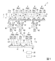
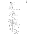
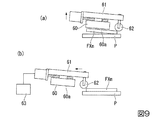
図1は第一実施形態のフィルム貼合システム1の概略構成図である。フィルム貼合システム1は、例えば液晶パネルや有機ELパネルといったパネル状の光学表示部品に、偏光フィルムや位相差フィルム、輝度上昇フィルムといったフィルム状の光学部材を貼合するもので、前記光学表示部品及び光学部材を含んだ光学表示デバイスを生産する生産システムの一部として構成される。フィルム貼合システム1では、前記光学表示部品として液晶パネルPを用いている。図1では図示都合上、フィルム貼合システム1を上下二段に分けて記載している。
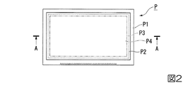
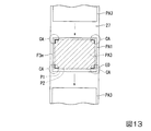
)から、その表示領域の外側の余剰部分を切り離すことにより形成されたものである。
これにより、各ロータリインデックス11,16(各貼合位置11c,11d,16c)に対する液晶パネルPのアライメントがなされる。
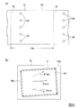
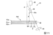
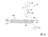
図9は、第二実施形態のフィルム貼合システムに適用される貼合装置の模式図である。
図9(a)は、シート片FXmを貼合ヘッド60に保持した状態を示す図であり、図9(b)は、シート片FXmを液晶パネルPに貼合した状態を示す図である。
上記実施形態では、切断装置41,42の一例としてCO2レーザーを用いたが、切断装置41,42はこれに限定されない。切断刃などの他の切断手段を切断装置41,42として用いることも可能である。
上記実施形態では、液晶パネルPに対するシート片FXmの貼合位置(相対貼合位置)の決定方法として、光学部材シートFXの面内の平均的な光学軸の方向を用いる方法を説明した。上記実施形態では、光学部材シートFXの面内の最大ずれ角θmaxと最小ずれ角θminとの平均値θmidを平均ずれ角とした場合に、光学部材シートFXのエッジラインに対して平均ずれ角θmidをなす方向を光学部材シートFXの面内の平均的な光学軸の方向として検出したが、光学部材シートFXの面内の平均的な光学軸の方向の検出方法はこれに限定されない。
上記実施形態では、液晶パネルPにシート片FXmを貼合する方法として貼合ヘッド32,60を用いる方法を説明したが、本発明はこれに限定されない。貼合ヘッド32,60を介さずに、ナイフエッジ31cでセパレータシートF3aから剥離されたシート片FXmを貼合ロールなどで直接液晶パネルPに貼合する方法を用いてもよい。
Claims (5)
- 光学表示部品に光学部材を貼合してなる光学表示デバイスの生産システムであって、
前記光学表示部品の表裏両面に前記光学表示部品の表示領域よりも大きい光学部材シートのシート片をそれぞれ貼合して貼合体とする貼合手段と、
前記貼合体において、前記シート片と前記光学表示部品との貼合面の外周縁を検出する検出装置と、
前記貼合体において、前記光学表示部品の表裏両面にそれぞれ貼合された前記シート片から前記貼合面に対応する部分の外側に配置された余剰部分を、前記外周縁に沿って切り離し、前記貼合面に対応する大きさの前記光学部材を前記光学表示部品の表裏両面にそれぞれ形成する切断手段と、を備えている光学表示デバイスの生産システム。 - 前記光学部材シートの光学軸方向の検査データに基づき、前記光学表示部品と前記シート片との相対貼合位置を決定する制御装置を備え、
前記貼合手段は、前記制御装置が決定した相対貼合位置に基づき、前記シート片を前記光学表示部品に貼合する請求項1に記載の光学表示デバイスの生産システム。 - 前記貼合手段は、光学部材シートを原反ロールからセパレータシートと共に巻き出す巻き出し部と、前記光学部材シートを前記セパレータシートを残してカットしてシート片とするカット部と、前記シート片を前記セパレータシートから剥離させる剥離部と、前記シート片を保持面に貼り付けて保持すると共に、前記保持面に保持した前記シート片を前記光学表示部品に貼合する貼合ヘッドと、を有する請求項1又は2に記載の光学表示デバイスの生産システム。
- 前記光学表示部品の表裏両面に貼合された前記シート片からそれぞれ切り離された前記余剰部分がまとめて前記光学表示部品から剥離される請求項1から3の何れか一項に記載の光学表示デバイスの生産システム。
- 前記切断手段は、前記光学表示部品の表裏一方の面に貼合されたシート片から前記余剰部分を切り離す第一切断装置と、前記光学表示部品の表裏他方の面に貼合されたシート片から前記余剰部分を切り離す第二切断装置と、を有し、
前記第一切断装置および前記第二切断装置は、レーザーカッターであり、
前記第一切断装置および前記第二切断装置は、同一のレーザー出力装置に接続されており、前記レーザー出力装置から出力されたレーザーが前記第一切断装置および前記第二切断装置に分岐されて供給される請求項1から4の何れか一項に記載の光学表示デバイスの生産システム。
Priority Applications (3)
| Application Number | Priority Date | Filing Date | Title |
|---|---|---|---|
| JP2013105589A JP6193618B2 (ja) | 2013-05-17 | 2013-05-17 | 光学表示デバイスの生産システム |
| TW103117260A TW201506491A (zh) | 2013-05-17 | 2014-05-16 | 光學顯示設備之生產系統 |
| PCT/JP2014/063048 WO2014185513A1 (ja) | 2013-05-17 | 2014-05-16 | 光学表示デバイスの生産システム |
Applications Claiming Priority (1)
| Application Number | Priority Date | Filing Date | Title |
|---|---|---|---|
| JP2013105589A JP6193618B2 (ja) | 2013-05-17 | 2013-05-17 | 光学表示デバイスの生産システム |
Publications (2)
| Publication Number | Publication Date |
|---|---|
| JP2014228564A true JP2014228564A (ja) | 2014-12-08 |
| JP6193618B2 JP6193618B2 (ja) | 2017-09-06 |
Family
ID=51898488
Family Applications (1)
| Application Number | Title | Priority Date | Filing Date |
|---|---|---|---|
| JP2013105589A Active JP6193618B2 (ja) | 2013-05-17 | 2013-05-17 | 光学表示デバイスの生産システム |
Country Status (3)
| Country | Link |
|---|---|
| JP (1) | JP6193618B2 (ja) |
| TW (1) | TW201506491A (ja) |
| WO (1) | WO2014185513A1 (ja) |
Citations (6)
| Publication number | Priority date | Publication date | Assignee | Title |
|---|---|---|---|---|
| JPH0887007A (ja) * | 1994-09-19 | 1996-04-02 | Ookubo Seisakusho:Kk | 偏光板の貼り付け装置 |
| JP2005043384A (ja) * | 2002-07-04 | 2005-02-17 | Fuji Photo Film Co Ltd | 偏光板貼合方法及び装置 |
| WO2006129523A1 (ja) * | 2005-05-30 | 2006-12-07 | Sharp Kabushiki Kaisha | 液晶表示装置の製造方法および液晶表示装置の製造装置 |
| JP2007288010A (ja) * | 2006-04-19 | 2007-11-01 | Lintec Corp | シート切断装置及び切断方法 |
| JP2012247714A (ja) * | 2011-05-30 | 2012-12-13 | V Technology Co Ltd | 基板への光学フィルム貼付装置 |
| JP2016013557A (ja) * | 2013-02-13 | 2016-01-28 | 住友化学株式会社 | レーザー光照射装置及び光学部材貼合体の製造装置 |
-
2013
- 2013-05-17 JP JP2013105589A patent/JP6193618B2/ja active Active
-
2014
- 2014-05-16 TW TW103117260A patent/TW201506491A/zh unknown
- 2014-05-16 WO PCT/JP2014/063048 patent/WO2014185513A1/ja not_active Ceased
Patent Citations (6)
| Publication number | Priority date | Publication date | Assignee | Title |
|---|---|---|---|---|
| JPH0887007A (ja) * | 1994-09-19 | 1996-04-02 | Ookubo Seisakusho:Kk | 偏光板の貼り付け装置 |
| JP2005043384A (ja) * | 2002-07-04 | 2005-02-17 | Fuji Photo Film Co Ltd | 偏光板貼合方法及び装置 |
| WO2006129523A1 (ja) * | 2005-05-30 | 2006-12-07 | Sharp Kabushiki Kaisha | 液晶表示装置の製造方法および液晶表示装置の製造装置 |
| JP2007288010A (ja) * | 2006-04-19 | 2007-11-01 | Lintec Corp | シート切断装置及び切断方法 |
| JP2012247714A (ja) * | 2011-05-30 | 2012-12-13 | V Technology Co Ltd | 基板への光学フィルム貼付装置 |
| JP2016013557A (ja) * | 2013-02-13 | 2016-01-28 | 住友化学株式会社 | レーザー光照射装置及び光学部材貼合体の製造装置 |
Also Published As
| Publication number | Publication date |
|---|---|
| WO2014185513A1 (ja) | 2014-11-20 |
| TW201506491A (zh) | 2015-02-16 |
| JP6193618B2 (ja) | 2017-09-06 |
Similar Documents
| Publication | Publication Date | Title |
|---|---|---|
| JP5692712B2 (ja) | 光学表示デバイスの生産システム | |
| CN104204918B (zh) | 光学显示设备的生产系统 | |
| TWI661928B (zh) | 光學顯示裝置之生產系統 | |
| JP5804404B2 (ja) | 光学表示デバイスの生産システム及び光学表示デバイスの生産方法 | |
| JP5724147B2 (ja) | 光学表示デバイスの生産システム | |
| JP6182805B2 (ja) | 光学表示デバイスの生産システム | |
| KR102110007B1 (ko) | 광학 표시 디바이스의 생산 시스템 및 생산 방법 | |
| WO2014129353A1 (ja) | 光学表示デバイスの生産システム及び生産方法 | |
| JP6223439B2 (ja) | 光学表示デバイスの生産システム | |
| JP5618283B2 (ja) | 光学表示デバイスの生産システム及び光学表示デバイスの生産方法 | |
| JP2014157344A (ja) | 光学表示デバイスの生産システム | |
| JP6193618B2 (ja) | 光学表示デバイスの生産システム |
Legal Events
| Date | Code | Title | Description |
|---|---|---|---|
| A621 | Written request for application examination |
Free format text: JAPANESE INTERMEDIATE CODE: A621 Effective date: 20160502 |
|
| A131 | Notification of reasons for refusal |
Free format text: JAPANESE INTERMEDIATE CODE: A131 Effective date: 20170104 |
|
| A521 | Request for written amendment filed |
Free format text: JAPANESE INTERMEDIATE CODE: A523 Effective date: 20170203 |
|
| TRDD | Decision of grant or rejection written | ||
| A01 | Written decision to grant a patent or to grant a registration (utility model) |
Free format text: JAPANESE INTERMEDIATE CODE: A01 Effective date: 20170801 |
|
| A61 | First payment of annual fees (during grant procedure) |
Free format text: JAPANESE INTERMEDIATE CODE: A61 Effective date: 20170810 |
|
| R150 | Certificate of patent or registration of utility model |
Ref document number: 6193618 Country of ref document: JP Free format text: JAPANESE INTERMEDIATE CODE: R150 |
|
| S531 | Written request for registration of change of domicile |
Free format text: JAPANESE INTERMEDIATE CODE: R313531 |
|
| R350 | Written notification of registration of transfer |
Free format text: JAPANESE INTERMEDIATE CODE: R350 |