JP2014228564A - Production system of optical display device - Google Patents
Production system of optical display device Download PDFInfo
- Publication number
- JP2014228564A JP2014228564A JP2013105589A JP2013105589A JP2014228564A JP 2014228564 A JP2014228564 A JP 2014228564A JP 2013105589 A JP2013105589 A JP 2013105589A JP 2013105589 A JP2013105589 A JP 2013105589A JP 2014228564 A JP2014228564 A JP 2014228564A
- Authority
- JP
- Japan
- Prior art keywords
- bonding
- sheet
- optical member
- sheet piece
- liquid crystal
- Prior art date
- Legal status (The legal status is an assumption and is not a legal conclusion. Google has not performed a legal analysis and makes no representation as to the accuracy of the status listed.)
- Granted
Links
Images
Classifications
-
- G—PHYSICS
- G02—OPTICS
- G02F—OPTICAL DEVICES OR ARRANGEMENTS FOR THE CONTROL OF LIGHT BY MODIFICATION OF THE OPTICAL PROPERTIES OF THE MEDIA OF THE ELEMENTS INVOLVED THEREIN; NON-LINEAR OPTICS; FREQUENCY-CHANGING OF LIGHT; OPTICAL LOGIC ELEMENTS; OPTICAL ANALOGUE/DIGITAL CONVERTERS
- G02F1/00—Devices or arrangements for the control of the intensity, colour, phase, polarisation or direction of light arriving from an independent light source, e.g. switching, gating or modulating; Non-linear optics
- G02F1/01—Devices or arrangements for the control of the intensity, colour, phase, polarisation or direction of light arriving from an independent light source, e.g. switching, gating or modulating; Non-linear optics for the control of the intensity, phase, polarisation or colour
- G02F1/13—Devices or arrangements for the control of the intensity, colour, phase, polarisation or direction of light arriving from an independent light source, e.g. switching, gating or modulating; Non-linear optics for the control of the intensity, phase, polarisation or colour based on liquid crystals, e.g. single liquid crystal display cells
- G02F1/1303—Apparatus specially adapted to the manufacture of LCDs
-
- G—PHYSICS
- G02—OPTICS
- G02F—OPTICAL DEVICES OR ARRANGEMENTS FOR THE CONTROL OF LIGHT BY MODIFICATION OF THE OPTICAL PROPERTIES OF THE MEDIA OF THE ELEMENTS INVOLVED THEREIN; NON-LINEAR OPTICS; FREQUENCY-CHANGING OF LIGHT; OPTICAL LOGIC ELEMENTS; OPTICAL ANALOGUE/DIGITAL CONVERTERS
- G02F1/00—Devices or arrangements for the control of the intensity, colour, phase, polarisation or direction of light arriving from an independent light source, e.g. switching, gating or modulating; Non-linear optics
- G02F1/01—Devices or arrangements for the control of the intensity, colour, phase, polarisation or direction of light arriving from an independent light source, e.g. switching, gating or modulating; Non-linear optics for the control of the intensity, phase, polarisation or colour
- G02F1/13—Devices or arrangements for the control of the intensity, colour, phase, polarisation or direction of light arriving from an independent light source, e.g. switching, gating or modulating; Non-linear optics for the control of the intensity, phase, polarisation or colour based on liquid crystals, e.g. single liquid crystal display cells
- G02F1/133—Constructional arrangements; Operation of liquid crystal cells; Circuit arrangements
- G02F1/1333—Constructional arrangements; Manufacturing methods
- G02F1/1335—Structural association of cells with optical devices, e.g. polarisers or reflectors
- G02F1/133504—Diffusing, scattering, diffracting elements
- G02F1/133507—Films for enhancing the luminance
-
- G—PHYSICS
- G02—OPTICS
- G02F—OPTICAL DEVICES OR ARRANGEMENTS FOR THE CONTROL OF LIGHT BY MODIFICATION OF THE OPTICAL PROPERTIES OF THE MEDIA OF THE ELEMENTS INVOLVED THEREIN; NON-LINEAR OPTICS; FREQUENCY-CHANGING OF LIGHT; OPTICAL LOGIC ELEMENTS; OPTICAL ANALOGUE/DIGITAL CONVERTERS
- G02F1/00—Devices or arrangements for the control of the intensity, colour, phase, polarisation or direction of light arriving from an independent light source, e.g. switching, gating or modulating; Non-linear optics
- G02F1/01—Devices or arrangements for the control of the intensity, colour, phase, polarisation or direction of light arriving from an independent light source, e.g. switching, gating or modulating; Non-linear optics for the control of the intensity, phase, polarisation or colour
- G02F1/13—Devices or arrangements for the control of the intensity, colour, phase, polarisation or direction of light arriving from an independent light source, e.g. switching, gating or modulating; Non-linear optics for the control of the intensity, phase, polarisation or colour based on liquid crystals, e.g. single liquid crystal display cells
- G02F1/133—Constructional arrangements; Operation of liquid crystal cells; Circuit arrangements
- G02F1/1333—Constructional arrangements; Manufacturing methods
- G02F1/1335—Structural association of cells with optical devices, e.g. polarisers or reflectors
- G02F1/133528—Polarisers
-
- G—PHYSICS
- G02—OPTICS
- G02F—OPTICAL DEVICES OR ARRANGEMENTS FOR THE CONTROL OF LIGHT BY MODIFICATION OF THE OPTICAL PROPERTIES OF THE MEDIA OF THE ELEMENTS INVOLVED THEREIN; NON-LINEAR OPTICS; FREQUENCY-CHANGING OF LIGHT; OPTICAL LOGIC ELEMENTS; OPTICAL ANALOGUE/DIGITAL CONVERTERS
- G02F1/00—Devices or arrangements for the control of the intensity, colour, phase, polarisation or direction of light arriving from an independent light source, e.g. switching, gating or modulating; Non-linear optics
- G02F1/01—Devices or arrangements for the control of the intensity, colour, phase, polarisation or direction of light arriving from an independent light source, e.g. switching, gating or modulating; Non-linear optics for the control of the intensity, phase, polarisation or colour
- G02F1/13—Devices or arrangements for the control of the intensity, colour, phase, polarisation or direction of light arriving from an independent light source, e.g. switching, gating or modulating; Non-linear optics for the control of the intensity, phase, polarisation or colour based on liquid crystals, e.g. single liquid crystal display cells
- G02F1/133—Constructional arrangements; Operation of liquid crystal cells; Circuit arrangements
- G02F1/1333—Constructional arrangements; Manufacturing methods
- G02F1/1335—Structural association of cells with optical devices, e.g. polarisers or reflectors
- G02F1/13363—Birefringent elements, e.g. for optical compensation
Landscapes
- Physics & Mathematics (AREA)
- Nonlinear Science (AREA)
- Liquid Crystal (AREA)
- Engineering & Computer Science (AREA)
- Manufacturing & Machinery (AREA)
- Chemical & Material Sciences (AREA)
- Crystallography & Structural Chemistry (AREA)
- General Physics & Mathematics (AREA)
- Optics & Photonics (AREA)
- Devices For Indicating Variable Information By Combining Individual Elements (AREA)
- Polarising Elements (AREA)
- Electroluminescent Light Sources (AREA)
Abstract
【課題】表示領域周辺の額縁部を縮小して表示エリアの拡大及び機器の小型化を図ることができる光学表示デバイスの生産システムを提供する。【解決手段】光学表示デバイスの生産システム(フィルム貼合システム1)は、光学表示部品Pの表裏両面に光学表示部品Pの表示領域よりも大きい光学部材シートF1,F2,F3のシート片をそれぞれ貼合する貼合装置13,15,18と、シート片と液晶パネルPとの貼合面の外周縁を検出する検出装置と、光学表示部品Pの表裏両面にそれぞれ貼合された前記シート片から貼合面に対応する部分の外側に配置された余剰部分を、外周縁に沿って切り離し、前記表示領域に対応する大きさの前記光学部材を光学表示部品Pの表裏両面にそれぞれ形成する切断手段40と、を備えている。【選択図】図1An optical display device production system capable of enlarging a display area and reducing the size of a device by reducing a frame portion around a display area. An optical display device production system (film bonding system 1) is provided with sheet pieces of optical member sheets F1, F2, and F3 larger than the display area of the optical display component P on both front and back surfaces of the optical display component P, respectively. Bonding devices 13, 15, and 18 to be bonded, a detection device for detecting the outer peripheral edge of the bonding surface between the sheet piece and the liquid crystal panel P, and the sheet pieces bonded to the front and back surfaces of the optical display component P, respectively. Cutting the excess part arranged on the outside of the part corresponding to the bonding surface from along the outer peripheral edge, and forming the optical member having a size corresponding to the display area on both the front and back surfaces of the optical display component P, respectively Means 40. [Selection] Figure 1
Description
本発明は、光学表示デバイスの生産システムに関するものである。 The present invention relates to an optical display device production system.
従来、液晶ディスプレイ等の光学表示デバイスの生産システムにおいて、液晶パネル(光学表示部品)に貼合する偏光板等の光学部材は、長尺フィルムから液晶パネルの表示領域に合わせたサイズのシート片に切り出され、梱包されて別ラインに搬送された後、液晶パネルに貼合されることがある(例えば、特許文献1参照)。 Conventionally, in a production system for an optical display device such as a liquid crystal display, an optical member such as a polarizing plate to be bonded to a liquid crystal panel (optical display component) is formed from a long film into a sheet piece having a size matching the display area of the liquid crystal panel. After being cut out, packed and transported to another line, it may be bonded to a liquid crystal panel (see, for example, Patent Document 1).
しかし、上記従来の構成では、液晶パネル及びシート片の各寸法バラツキ、並びに液晶パネルに対するシート片の貼合バラツキ(位置ズレ)を考慮して、表示領域よりも若干大きめのシート片を切り出している。そのため、表示領域の周辺部に余分な領域(額縁部)が形成され、機器の小型化が阻害されるという問題がある。 However, in the conventional configuration described above, a sheet piece slightly larger than the display area is cut out in consideration of variation in dimensions of the liquid crystal panel and the sheet piece, and bonding variation (positional deviation) of the sheet piece to the liquid crystal panel. . Therefore, there is a problem that an extra area (frame part) is formed around the display area, and downsizing of the device is hindered.
本発明の目的は、表示領域周辺の額縁部を縮小して表示エリアの拡大及び機器の小型化を図ることができる光学表示デバイスの生産システムを提供することにある。 An object of the present invention is to provide a production system for an optical display device capable of reducing the frame portion around the display area to enlarge the display area and downsize the device.
本発明の光学表示デバイスの生産システムは、光学表示部品に光学部材を貼合してなる光学表示デバイスの生産システムであって、前記光学表示部品の表裏両面に前記光学表示部品の表示領域よりも大きい光学部材シートのシート片をそれぞれ貼合して貼合体とする貼合手段と、前記貼合体において、前記シート片と前記光学表示部品との貼合面の外周縁を検出する検出装置と、前記貼合体において、前記光学表示部品の表裏両面にそれぞれ貼合された前記シート片から、前記貼合面に対応する部分の外側に配置された余剰部分を、前記外周縁に沿って切り離し、前記貼合面に対応する大きさの前記光学部材を前記光学表示部品の表裏両面にそれぞれ形成する切断手段と、を備えている。 An optical display device production system according to the present invention is an optical display device production system in which an optical member is bonded to an optical display component. A detecting means for detecting an outer peripheral edge of a bonding surface between the sheet piece and the optical display component in the bonding means, in which the sheet pieces of the large optical member sheet are bonded to each other to form a bonded body, In the bonded body, from the sheet pieces bonded respectively to the front and back surfaces of the optical display component, the excess portion disposed outside the portion corresponding to the bonded surface is cut along the outer peripheral edge, Cutting means for forming the optical member having a size corresponding to the bonding surface on both the front and back surfaces of the optical display component.
ここで、「シート片と光学表示部品との貼合面」とは、光学表示部品においてシート片と対向する面を指し、「貼合面の外周縁」とは、具体的には、光学表示部品においてシート片が貼合された側の基板の外周縁を指す。 Here, the “bonding surface between the sheet piece and the optical display component” refers to a surface facing the sheet piece in the optical display component, and “the outer peripheral edge of the bonding surface” specifically refers to an optical display. The outer peripheral edge of the board | substrate of the side by which the sheet piece was bonded in components is pointed out.
また、シート片の「貼合面に対応する部分」とは、シート片において、シート片と対向する光学表示部品の表示領域の大きさ以上、光学表示部品の外形状(平面視における輪郭形状)の大きさ以下の領域であって、かつ光学表示部品における電気部品取付部等の機能部分を避けた領域を指す。同様に「貼合面に対応する大きさ」とは、光学表示部品の表示領域の大きさ以上、光学表示部品の外形状(平面視における輪郭形状)の大きさ以下の大きさであって、かつ光学表示部品における電気部品取付部等の機能部分を避けた大きさを指す。 Further, the “part corresponding to the bonding surface” of the sheet piece means that the outer shape of the optical display component (contour shape in plan view) is not less than the size of the display area of the optical display component facing the sheet piece. Is a region that is smaller than the size of the optical display component and avoids a functional portion such as an electrical component mounting portion in the optical display component. Similarly, the “size corresponding to the bonding surface” is a size not less than the size of the display area of the optical display component and not more than the size of the outer shape (contour shape in plan view) of the optical display component, In addition, it refers to a size that avoids a functional part such as an electric part mounting part in the optical display part.
前記光学部材シートの光学軸方向の検査データに基づき、前記光学表示部品と前記シート片との相対貼合位置を決定する制御装置を備え、前記貼合手段は、前記制御装置が決定した相対貼合位置に基づき、前記シート片を前記光学表示部品に貼合してもよい。 Based on the inspection data in the optical axis direction of the optical member sheet, a control device for determining a relative bonding position between the optical display component and the sheet piece is provided, and the bonding means is a relative bonding determined by the control device. The sheet piece may be bonded to the optical display component based on the alignment position.
前記貼合手段は、光学部材シートを原反ロールからセパレータシートと共に巻き出す巻き出し部と、前記光学部材シートを前記セパレータシートを残してカットしてシート片とするカット部と、前記シート片を前記セパレータシートから剥離させる剥離部と、前記シート片を保持面に貼り付けて保持すると共に、前記保持面に保持した前記シート片を前記光学表示部品に貼合する貼合ヘッドと、を有してもよい。 The bonding means includes an unwinding unit for unwinding the optical member sheet together with the separator sheet from the raw roll, a cutting unit that cuts the optical member sheet leaving the separator sheet to form a sheet piece, and the sheet piece. A peeling part that peels from the separator sheet, and a bonding head that bonds and holds the sheet piece on a holding surface and bonds the sheet piece held on the holding surface to the optical display component. May be.
前記光学表示部品の表裏両面に貼合された前記シート片からそれぞれ切り離された前記余剰部分がまとめて前記光学表示部品から剥離されてもよい。 The surplus parts cut off from the sheet pieces bonded to the front and back surfaces of the optical display component may be collectively peeled from the optical display component.
前記切断手段は、前記光学表示部品の表裏一方の面に貼合されたシート片から前記余剰部分を切り離す第一切断装置と、前記光学表示部品の表裏他方の面に貼合されたシート片から前記余剰部分を切り離す第二切断装置と、を有し、前記第一切断装置および前記第二切断装置は、レーザーカッターであり、前記第一切断装置および前記第二切断装置は、同一のレーザー出力装置に接続されており、前記レーザー出力装置から出力されたレーザーが前記第一切断装置および前記第二切断装置に分岐されて供給されてもよい。 The cutting means includes a first cutting device that separates the surplus portion from a sheet piece bonded to one surface of the optical display component, and a sheet piece bonded to the other surface of the optical display component. A second cutting device for cutting off the surplus portion, wherein the first cutting device and the second cutting device are laser cutters, and the first cutting device and the second cutting device have the same laser output The laser output from the laser output device may be branched and supplied to the first cutting device and the second cutting device.
本発明によれば、表示領域周辺の額縁部を縮小して表示エリアの拡大及び機器の小型化を図ることができる光学表示デバイスの生産システムを提供することができる。 ADVANTAGE OF THE INVENTION According to this invention, the production system of the optical display device which can aim at expansion of a display area and size reduction of an apparatus can be provided by reducing the frame part around a display area.
以下、本発明の実施形態について図面を参照して説明する。本実施形態では、光学表示デバイスの生産システムとして、その一部を構成するフィルム貼合システムについて説明する。 Embodiments of the present invention will be described below with reference to the drawings. This embodiment demonstrates the film bonding system which comprises the one part as a production system of an optical display device.
[第一実施形態]
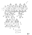
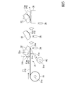
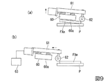
図1は第一実施形態のフィルム貼合システム1の概略構成図である。フィルム貼合システム1は、例えば液晶パネルや有機ELパネルといったパネル状の光学表示部品に、偏光フィルムや位相差フィルム、輝度上昇フィルムといったフィルム状の光学部材を貼合するもので、前記光学表示部品及び光学部材を含んだ光学表示デバイスを生産する生産システムの一部として構成される。フィルム貼合システム1では、前記光学表示部品として液晶パネルPを用いている。図1では図示都合上、フィルム貼合システム1を上下二段に分けて記載している。
[First embodiment]
Drawing 1 is a schematic structure figure of
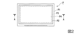
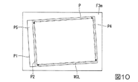
図2は液晶パネルPをその液晶層P3の厚さ方向から見た平面図である。液晶パネルPは、平面視で長方形状をなす第一基板P1と、第一基板P1に対向して配置される比較的小形の長方形状をなす第二基板P2と、第一基板P1と第二基板P2との間に封入された液晶層P3とを備える。液晶パネルPは、平面視で第一基板P1の外形状に沿う長方形状をなし、平面視で液晶層P3の外周の内側に収まる領域を表示領域P4とする。 FIG. 2 is a plan view of the liquid crystal panel P viewed from the thickness direction of the liquid crystal layer P3. The liquid crystal panel P includes a first substrate P1 that has a rectangular shape in plan view, a second substrate P2 that has a relatively small rectangular shape disposed to face the first substrate P1, a first substrate P1, and a second substrate. And a liquid crystal layer P3 sealed between the substrate P2. The liquid crystal panel P has a rectangular shape that conforms to the outer shape of the first substrate P1 in plan view, and a region that fits inside the outer periphery of the liquid crystal layer P3 in plan view is defined as a display region P4.
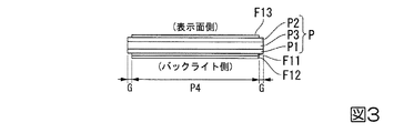
図3は図2のA−A断面図である。液晶パネルPの表裏面には、長尺帯状の第一、第二及び第三光学部材シートF1,F2,F3(図1参照、以下、光学部材シートFXと総称することがある。)から切り出した第一、第二及び第三光学部材F11,F12,F13(以下、光学部材F1Xと総称することがある。)が適宜貼合される。本実施形態では、液晶パネルPのバックライト側及び表示面側の両面には、偏光フィルムとしての第一光学部材F11及び第三光学部材F13がそれぞれ貼合され、液晶パネルPのバックライト側の面には、第一光学部材F11に重ねて輝度向上フィルムとしての第二光学部材F12がさらに貼合される。 3 is a cross-sectional view taken along the line AA in FIG. The front and back surfaces of the liquid crystal panel P are cut out from the first, second, and third optical member sheets F1, F2, and F3 (refer to FIG. 1; hereinafter, sometimes collectively referred to as the optical member sheet FX) having a long strip shape. The first, second, and third optical members F11, F12, and F13 (hereinafter may be collectively referred to as the optical member F1X) are appropriately bonded. In the present embodiment, the first optical member F11 and the third optical member F13 as polarizing films are bonded to both the backlight side and the display surface side of the liquid crystal panel P, respectively. On the surface, a second optical member F12 as a brightness enhancement film is further bonded to the first optical member F11.
なお、第一、第二及び第三光学部材F11,F12,F13は、後述する第一、第二及び第三シート片F1m,F2m,F3m(以下、シート片FXmと総称することがある。
)から、その表示領域の外側の余剰部分を切り離すことにより形成されたものである。
The first, second, and third optical members F11, F12, and F13 may be collectively referred to as first, second, and third sheet pieces F1m, F2m, and F3m (hereinafter referred to as sheet pieces FXm).
) From the excess area outside the display area.
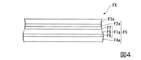
図4は液晶パネルPに貼合する光学部材シートFXの部分断面図である。光学部材シートFXは、フィルム状の光学部材本体F1aと、光学部材本体F1aの一方の面(図4では上面)に設けられた粘着層F2aと、粘着層F2aを介して光学部材本体F1aの一方の面に分離可能に積層されたセパレータシートF3aと、光学部材本体F1aの他方の面(図4では下面)に積層された表面保護フィルムF4aとを有する。光学部材本体F1aは偏光板として機能し、液晶パネルPの表示領域P4の全域とその周辺領域とにわたって貼合される。なお、図示都合上、図4の各層のハッチングは略す。 FIG. 4 is a partial cross-sectional view of the optical member sheet FX bonded to the liquid crystal panel P. The optical member sheet FX includes a film-shaped optical member main body F1a, an adhesive layer F2a provided on one surface (the upper surface in FIG. 4) of the optical member main body F1a, and one of the optical member main bodies F1a via the adhesive layer F2a. The separator sheet F3a is detachably stacked on the surface, and the surface protection film F4a is stacked on the other surface (the lower surface in FIG. 4) of the optical member body F1a. The optical member main body F1a functions as a polarizing plate, and is bonded over the entire display area P4 of the liquid crystal panel P and its peripheral area. For convenience of illustration, hatching of each layer in FIG. 4 is omitted.
光学部材本体F1aは、その一方の面に粘着層F2aを残しつつセパレータシートF3aを分離させした状態で、液晶パネルPに粘着層F2aを介して貼合される。以下、光学部材シートFXからセパレータシートF3aを除いた部分を貼合シートF5という。 The optical member body F1a is bonded to the liquid crystal panel P via the adhesive layer F2a in a state where the separator sheet F3a is separated while leaving the adhesive layer F2a on one surface thereof. Hereinafter, the part remove | excluding the separator sheet F3a from the optical member sheet | seat FX is called the bonding sheet | seat F5.
セパレータシートF3aは、粘着層F2aから分離されるまでの間に粘着層F2a及び光学部材本体F1aを保護する。表面保護フィルムF4aは、光学部材本体F1aと共に液晶パネルPに貼合される。表面保護フィルムF4aは、光学部材本体F1aに対して液晶パネルPと反対側に配置されて光学部材本体F1aを保護する。表面保護フィルムF4aは、所定のタイミングで光学部材本体F1aから分離される。なお、光学部材シートFXが表面保護フィルムF4aを含まない構成であったり、表面保護フィルムF4aが光学部材本体F1aから分離されない構成であってもよい。 The separator sheet F3a protects the adhesive layer F2a and the optical member body F1a before being separated from the adhesive layer F2a. The surface protective film F4a is bonded to the liquid crystal panel P together with the optical member body F1a. The surface protective film F4a is disposed on the side opposite to the liquid crystal panel P with respect to the optical member body F1a to protect the optical member body F1a. The surface protective film F4a is separated from the optical member main body F1a at a predetermined timing. The optical member sheet FX may be configured not to include the surface protective film F4a, or the surface protective film F4a may not be separated from the optical member main body F1a.
光学部材本体F1aは、シート状の偏光子F6と、偏光子F6の一方の面に接着剤等で接合される第一フィルムF7と、偏光子F6の他方の面に接着剤等で接合される第二フィルムF8とを有する。第一フィルムF7及び第二フィルムF8は、例えば偏光子F6を保護する保護フィルムである。 The optical member body F1a is bonded to the sheet-like polarizer F6, the first film F7 bonded to one surface of the polarizer F6 with an adhesive or the like, and the other surface of the polarizer F6 with an adhesive or the like. And a second film F8. The first film F7 and the second film F8 are protective films that protect the polarizer F6, for example.
なお、光学部材本体F1aは、一層の光学層からなる単層構造でもよく、複数の光学層が互いに積層された積層構造でもよい。前記光学層は、偏光子F6の他に、位相差フィルムや輝度向上フィルム等でもよい。第一フィルムF7と第二フィルムF8の少なくとも一方は、液晶表示素子の最外面を保護するハードコート処理やアンチグレア処理を含む防眩などの効果が得られる表面処理が施されてもよい。光学部材本体F1aは、第一フィルムF7と第二フィルムF8の少なくとも一方を含まなくてもよい。例えば第一フィルムF7を省略した場合、セパレータシートF3aを光学部材本体F1aの一方の面に粘着層F2aを介して貼り合わせてもよい。 The optical member main body F1a may have a single-layer structure composed of a single optical layer or a stacked structure in which a plurality of optical layers are stacked on each other. In addition to the polarizer F6, the optical layer may be a retardation film, a brightness enhancement film, or the like. At least one of the first film F7 and the second film F8 may be subjected to a surface treatment that provides an effect such as anti-glare including hard coat treatment and anti-glare treatment for protecting the outermost surface of the liquid crystal display element. The optical member body F1a may not include at least one of the first film F7 and the second film F8. For example, when the first film F7 is omitted, the separator sheet F3a may be bonded to one surface of the optical member body F1a via the adhesive layer F2a.
以下、図1を参照してフィルム貼合システム1について説明する。なお、図中矢印Fは液晶パネルPの搬送方向を示す。以下の説明では、液晶パネルPの搬送方向上流側をパネル搬送上流側、液晶パネルPの搬送方向下流側をパネル搬送下流側という。
Hereinafter, the
フィルム貼合システム1は、第一ロータリインデックス11と、第一ロータリインデックス11の第一ロータリ始発位置11aへ液晶パネルPを搬送する搬送装置12と、第一ロータリインデックス11の周囲に設けられる第一及び第二貼合装置13,15並びにフィルム剥離装置14と、第一ロータリインデックス11のパネル搬送下流側に設けられる第二ロータリインデックス16と、第一ロータリインデックス11の第一ロータリ終着位置11bから第二ロータリインデックス16の第二ロータリ始発位置16aへ液晶パネルPを表裏を反転させつつ搬送する搬送装置17と、第二ロータリインデックス16の周囲に設けられる第三貼合装置18とを備える。
The
また、フィルム貼合システム1は、第二ロータリインデックス16のパネル搬送下流側に設けられるコンベヤ27と、第二ロータリインデックス16の第二ロータリ終着位置16bからコンベヤ27の始発位置27aへ液晶パネルPを搬送する搬送装置21と、コンベヤ27の搬送経路上に設けられた第一切断装置41と、コンベヤ27の搬送下流側に設けられるコンベヤ28と、コンベヤ27の終着位置27bからコンベヤ28の始発位置28aへ液晶パネルPを表裏を反転させつつ搬送する搬送装置22と、コンベヤ28の搬送経路上に設けられた第二切断装置42とを備える。
In addition, the
第一貼合装置13、第二貼合装置15および第三貼合装置18は、液晶パネルPの表裏両面に液晶パネルPの表示領域P4よりも大きい光学部材シートFXのシート片FXmをそれぞれ貼合する貼合手段を構成する。また、第一切断装置41および第二切断装置42は、液晶パネルPの表裏両面にそれぞれ貼合されたシート片FXmから、液晶パネルPとシート片FXmとの貼合面の外周縁に対応する部分の外側に配置された余剰部分を切り離し、液晶パネルPとシート片FXmとの貼合面の外周縁に対応する大きさの光学部材F1Xを液晶パネルPの表裏両面にそれぞれ形成する切断手段を構成する。
The
また、詳しくは後述するが、第一切断装置41のパネル搬送上流側には、第一切断装置41におけるカット位置を設定するために用いる検出装置が設けられ、第二切断装置42のパネル搬送上流側には、第二切断装置42におけるカット位置を設定するために用いる検出装置が設けられている。
Further, as will be described in detail later, a detection device used for setting a cutting position in the
フィルム貼合システム1は、ロータリインデックス11,16およびコンベヤ27,28が形成するラインを用いて液晶パネルPを搬送しつつ、液晶パネルPに順次所定の処理を施す。液晶パネルPは、その表裏面を水平にした状態でライン上を搬送され、その表裏面に対して、帯状の光学部材シートFXから所定長さに切り出した貼合シートF5のシート片(光学部材F1Xに相当)が貼合される。フィルム貼合システム1の各部は、電子制御装置としての制御装置25により統括制御される。
The
搬送装置12は、液晶パネルPを保持して垂直方向及び水平方向で自在に搬送する。搬送装置12は、例えば吸着によって保持した液晶パネルPを第一ロータリインデックス11の第一ロータリ始発位置11aへ水平状態のまま搬送し、当該位置で前記吸着を解除して液晶パネルPを第一ロータリインデックス11に受け渡す。
The
第一ロータリインデックス11は、鉛直方向に沿う回転軸を有する円盤状の回転テーブルであり、搬送装置12からの搬入位置を第一ロータリ始発位置11aとして例えば右回りに回転駆動する。第一ロータリインデックス11は、第一ロータリ始発位置11aから例えば右回りに所定角度だけ回転した位置を第一貼合位置11cとする。この第一貼合位置11cにて、第一貼合装置13によるバックライト側の第一シート片F1mの貼合がなされる。第一シート片F1mは、液晶パネルPの表示領域よりも大きいサイズの第一光学部材シートF1のシート片である。第一貼合装置13により液晶パネルPの表裏一方の面に第一シート片F1mが貼合されることにより、第一光学部材貼合体PA1が形成される。
The first
第一ロータリインデックス11は、第一貼合位置11cから例えば右回りに所定角度だけ回転した位置をフィルム剥離位置11eとする。このフィルム剥離位置11eにて、フィルム剥離装置14による第一シート片F1mの表面保護フィルムF4aの剥離がなされる。
The 1st
第一ロータリインデックス11は、フィルム剥離位置11eから例えば右回りに所定角度だけ回転した位置を第二貼合位置11dとする。この第二貼合位置11dにて、第二貼合装置15によるバックライト側の第二シート片F2mの貼合がなされる。第二シート片F2mは、液晶パネルPの表示領域よりも大きいサイズの第二光学部材シートF2のシート片である。第二貼合装置15により第一光学部材貼合体PA1の第一シート片F1m側の面に第二シート片F2mが貼合されることにより、第二光学部材貼合体PA2が形成される。
The 1st
第一ロータリインデックス11は、第二貼合位置11dから例えば右回りに所定角度だけ回転した位置を第一ロータリ終着位置11bとする。この第一ロータリ終着位置11bにて、搬送装置17による第二光学部材貼合体PA2の搬出がなされる。
The 1st
搬送装置17は、液晶パネルP(第二光学部材貼合体PA2)を保持して垂直方向及び水平方向で自在に搬送する。搬送装置17は、例えば吸着によって保持した液晶パネルPを第二ロータリインデックス16の第二ロータリ始発位置16aへ搬送すると共に、この搬送時に液晶パネルPの表裏を反転し、第二ロータリ始発位置16aで前記吸着を解除して液晶パネルPを第二ロータリインデックス16に受け渡す。
The
第二ロータリインデックス16は、鉛直方向に沿う回転軸を有する円盤状の回転テーブルであり、搬送装置17からの搬入位置を第二ロータリ始発位置16aとして例えば右回りに回転駆動する。第二ロータリインデックス16は、第二ロータリ始発位置16aから例えば右回りに所定角度だけ回転した位置を第三貼合位置16cとする。この第三貼合位置16cにて、第三貼合装置18による表示面側の第三シート片F3mの貼合がなされる。第三シート片F3mは、液晶パネルPの表示領域よりも大きいサイズの第三光学部材シートF3のシート片である。第三貼合装置18により液晶パネルPの表裏他方の面(第二光学部材貼合体PA2の第一シート片F1mおよび第二シート片F2mが貼合された面とは反対側の面)に第三シート片F3mが貼合されることにより、第三光学部材貼合体PA3が形成される。
The second
ここで、シート片FXm(第一シート片F1m、第二シート片F2mおよび第三シート片F3m)のそれぞれの大きさは、例えば液晶パネルPよりも大きいものとすることができる。なお、シート片FXmにおいて、液晶パネルPの外側にはみ出る部分の大きさ(シート片FXmの余剰部分の大きさ)は、液晶パネルPのサイズに応じて適宜設定される。例えば、シート片FXmを5インチ〜10インチの中小型サイズの液晶パネルPに適用する場合は、シート片FXmの各辺においてシート片FXmの一辺と液晶パネルPの一辺との間の間隔を2mm〜5mmの範囲の長さに設定する。 Here, the size of each of the sheet pieces FXm (the first sheet piece F1m, the second sheet piece F2m, and the third sheet piece F3m) may be larger than the liquid crystal panel P, for example. In the sheet piece FXm, the size of the portion that protrudes outside the liquid crystal panel P (the size of the surplus portion of the sheet piece FXm) is appropriately set according to the size of the liquid crystal panel P. For example, when the sheet piece FXm is applied to a medium-to-small size liquid crystal panel P of 5 to 10 inches, the distance between one side of the sheet piece FXm and one side of the liquid crystal panel P is 2 mm on each side of the sheet piece FXm. Set to a length in the range of ~ 5 mm.
第二ロータリインデックス16は、第三貼合位置16cから例えば右回りに所定角度だけ回転した位置を第二ロータリ終着位置16bとする。この第二ロータリ終着位置16bにて、搬送装置21による第三光学部材貼合体PA3の搬出がなされる。
The 2nd
搬送装置21は、液晶パネルP(第三光学部材貼合体PA3)を保持して垂直方向及び水平方向で自在に搬送する。搬送装置21は、例えば吸着によって保持した液晶パネルPをコンベヤ27の始発位置27aへ搬送し、始発位置27aで前記吸着を解除して液晶パネルPをコンベヤ27に受け渡す。
The conveying
コンベヤ27の始発位置27a以降の搬送経路上には、第一切断位置27cが設定されている。この第一切断位置27cにて、第一切断装置41による第三シート片F3mの切断が行われる。第一切断装置41は、液晶パネルPに貼合された第三シート片F3mから液晶パネルPと第三シート片F3mとの貼合面に対応する部分の外側に配置された余剰部分を切り離し、液晶パネルPと第三シート片F3mとの貼合面に対応する大きさの光学部材(第三光学部材F13)を形成する。
A
第一切断装置41により第三光学部材貼合体PA3から第三シート片F3mの余剰部分が切り離されることにより、液晶パネルPの表裏他方の面に第三光学部材F13が貼合され、且つ、液晶パネルPの表裏一方の面に第一シート片F1mおよび第二シート片F2mが貼合されてなる第四光学部材貼合体PA4が形成される。第三シート片F3mから切り離された余剰部分は、図示略の剥離装置によって液晶パネルPから剥離され回収される。
The third optical member F13 is bonded to the other surface of the liquid crystal panel P by separating the excess portion of the third sheet piece F3m from the third optical member bonding body PA3 by the
搬送装置22は、液晶パネルP(第四光学部材貼合体PA4)を保持して垂直方向及び水平方向で自在に搬送する。搬送装置22は、例えば吸着によって保持した液晶パネルPをコンベヤ28の始発位置28aへ搬送し、始発位置28aで前記吸着を解除して液晶パネルPをコンベヤ28に受け渡す。
The
コンベヤ28の始発位置28a以降の搬送経路上には、第二切断位置28bが設定されている。この第二切断位置28bにて、第二切断装置42よる第一シート片F1mおよび第二シート片F2mの切断が行われる。第二切断装置42は、液晶パネルPに貼合された第一シート片F1m及び第二シート片F2mのそれぞれから液晶パネルPと、第一シート片F1mおよび第二シート片F2mの積層体との貼合面に対応する部分の外側に配置された余剰部分をまとめて切り離し、第一光学部材シートF1からなる第一光学部材F11及び第二光学部材シートF2からなる第二光学部材F12を、液晶パネルPと、第一シート片F1mおよび第二シート片F2mの積層体との貼合面に対応する大きさの光学部材として形成する。
A second cutting position 28 b is set on the conveyance path after the initial position 28 a of the
第一シート片F1mと第二シート片F2mを液晶パネルPに貼合した後にまとめてカットすることで、第一光学部材F11と第二光学部材F12との位置ずれがなくなり、表示領域P4の外周縁の形状に合った第一光学部材F11および第二光学部材F12が得られる。また、第一シート片F1mと第二シート片F2mの切断工程も簡略化される。 By bonding the first sheet piece F1m and the second sheet piece F2m to the liquid crystal panel P and then cutting them together, the first optical member F11 and the second optical member F12 are not misaligned, and the outside of the display area P4. The first optical member F11 and the second optical member F12 that match the shape of the periphery are obtained. Moreover, the cutting process of the 1st sheet piece F1m and the 2nd sheet piece F2m is also simplified.
第二切断装置42により第四光学部材貼合体PA4から第一シート片F1m及び第二シート片F2mの余剰部分が切り離されることにより、液晶パネルPの表裏一方の面に第一光学部材F11および第二光学部材F12が貼合され、且つ、液晶パネルPの表裏他方の面に第三光学部材F13が貼合されてなる第五光学部材貼合体が形成される。第一シート片FX1および第二シート片F2mから切り離された余剰部分は、図示略の剥離装置によって液晶パネルPから剥離され回収される。
The
ここで、第一切断装置41および第二切断装置42は、例えばCO2レーザーカッターである。第一切断装置41および第二切断装置42は、液晶パネルPに貼合されたシート片FXmを表示領域P4の外周縁に沿って無端状に切断する。第一切断装置41と第二切断装置42は、同一のレーザー出力装置43に接続されている。第一切断装置41、第二切断装置42およびレーザー出力装置43によって、シート片FXmから、液晶パネルPとシート片FXmとの貼合面に対応する部分の外側に配置された余剰部分を切り離し、液晶パネルPとシート片FXmとの貼合面に対応する大きさの光学部材F1Xを形成する切断手段40が構成されている。各シート片F1m,F2m,F3mの切断に必要なレーザー出力はそれほど大きくないため、本実施形態では、レーザー出力装置43から出力された高出力のレーザー光を二つに分岐して第一切断装置41と第二切断装置42に供給している。
Here, the
第二切断位置28b以降の液晶パネルP(第五光学部材貼合体)の搬送経路上には図示略の貼合検査位置が設置されており、この貼合検査位置にて、フィルム貼合がなされたワーク(液晶パネルP)の図示略の検査装置による検査(光学部材F1Xの位置が適正か否か(位置ズレが公差範囲内にあるか否か)等の検査)がなされる。液晶パネルPに対する光学部材F1Xの位置が適正ではないと判定されたワークは、不図示の払い出し手段によりシステム外に排出される。 A bonding inspection position (not shown) is installed on the transport path of the liquid crystal panel P (fifth optical member bonding body) after the second cutting position 28b, and film bonding is performed at this bonding inspection position. The workpiece (liquid crystal panel P) is inspected by an inspection device (not shown) (inspection of whether or not the position of the optical member F1X is appropriate (whether the positional deviation is within the tolerance range)). The work determined that the position of the optical member F1X with respect to the liquid crystal panel P is not appropriate is discharged out of the system by a not-shown discharging means.
以上をもってフィルム貼合システム1による貼合工程が完了する。
With the above, the bonding process by the
以下、図5を参照して第一貼合装置13の詳細について説明する。なお、第二及び第三貼合装置15,18も同様の構成を有するものとしてその詳細説明は省略する。
Hereinafter, the detail of the
第一貼合装置13は、第一貼合位置11cに搬送された液晶パネルPの上面に対して、第一光学部材シートF1における所定サイズにカットした貼合シートF5のシート片(第一シート片F1m)の貼合を行う。
The
第一貼合装置13は、第一光学部材シートF1が巻回された原反ロールR1から第一光学部材シートF1を巻き出しつつ第一光学部材シートF1をその長手方向に沿って搬送するシート搬送装置31と、シート搬送装置31が第一光学部材シートF1から切り出した貼合シートF5のシート片(第一シート片F1m)を保持すると共にこのシート片を第一貼合位置11cに搬送された液晶パネルPの上面に貼合する貼合ヘッド32とを備える。
The
シート搬送装置31は、セパレータシートF3aをキャリアとして貼合シートF5を搬送するもので、帯状の第一光学部材シートF1を巻回した原反ロールR1を保持すると共に第一光学部材シートF1をその長手方向に沿って繰り出す巻き出し部31aと、原反ロールR1から巻き出した第一光学部材シートF1にハーフカットを施すカット部31bと、ハーフカットを施した第一光学部材シートF1を鋭角に巻きかけてセパレータシートF3aから貼合シートF5を分離させるナイフエッジ(剥離部)31cと、ナイフエッジ31cを経て単独となったセパレータシートF3aを巻き取るセパレータロールR2を保持する巻き取り部31dとを有する。
The
なお、図示は略すが、シート搬送装置31は第一光学部材シートF1を所定の搬送経路に沿うように巻きかける複数のガイドローラを有する。第一光学部材シートF1は、その搬送方向と直交する水平方向(シート幅方向)で、液晶パネルPの表示領域P4の幅(表示領域P4の長辺と短辺のうちいずれか一方の辺の長さ。本実施形態では表示領域P4の長辺長さに相当)よりも広い幅を有している。
In addition, although illustration is abbreviate | omitted, the
シート搬送装置31の始点に位置する巻き出し部31aとシート搬送装置31の終点に位置する巻き取り部31dとは、例えば互いに同期して駆動する。これにより、巻き出し部31aが第一光学部材シートF1をその搬送方向へ繰り出しつつ、巻き取り部31dがナイフエッジ31cを経たセパレータシートF3aを巻き取る。以下、シート搬送装置31における第一光学部材シートF1(セパレータシートF3a)の搬送方向上流側をシート搬送上流側、搬送方向下流側をシート搬送下流側という。
The unwinding
カット部31bは、第一光学部材シートF1が前記シート幅方向と直交する長さ方向で表示領域P4の長さ(表示領域P4の長辺と短辺のうちいずれか他方の辺の長さ。本実施形態では表示領域P4の短辺長さに相当)よりも長い長さが繰り出される毎に、前記シート幅方向に沿って全幅にわたって第一光学部材シートF1の厚さ方向の一部を切断する(ハーフカットを施す)。これにより、第一光学部材シートF1から液晶パネルPの表示領域P4よりも大きい貼合シートF5のシート片(第一シート片F1m)が切り出される。
The
カット部31bは、第一光学部材シートF1の搬送中に働くテンションによって第一光学部材シートF1(セパレータシートF3a)が破断しないように(所定の厚さがセパレータシートF3aに残るように)、切断刃の進退位置を調整し、粘着層F2aとセパレータシートF3aとの界面の近傍まで前記ハーフカットを施す。なお、切断刃に代わるレーザー装置を用いてもよい。
The
ハーフカット後の第一光学部材シートF1には、その厚さ方向で光学部材本体F1a及び表面保護フィルムF4aが切断されることにより、第一光学部材シートF1のシート幅方向の全幅にわたる切込線が形成される。第一光学部材シートF1は、前記切込線によって長手方向で表示領域P4の短辺長さ相当の長さを有する区画に分けられる。この区画が、それぞれ貼合シートF5における一つのシート片(第一シート片F1m)となる。 The first optical member sheet F1 after the half cut is cut along the entire width in the sheet width direction of the first optical member sheet F1 by cutting the optical member body F1a and the surface protection film F4a in the thickness direction. Is formed. The first optical member sheet F1 is divided into sections having a length corresponding to the short side length of the display region P4 in the longitudinal direction by the cut line. Each section is one sheet piece (first sheet piece F1m) in the bonding sheet F5.
ナイフエッジ31cは、その鋭角状の先端部に第一光学部材シートF1を鋭角に巻きかける。第一光学部材シートF1は、ナイフエッジ31cの先端部で鋭角に折り返す際、第一シート片F1mからセパレータシートF3aを剥離する。このとき、第一シート片F1mの粘着層F2a(液晶パネルPとの貼合面)は下向きとなる。ナイフエッジ31cの先端部の直上はセパレータ剥離位置31eとなり、このナイフエッジ31cの先端部に貼合ヘッド32の円弧状の保持面32aが上方から接することで、第一シート片F1mの表面保護フィルムF4a(貼合面と反対側の面)が貼合ヘッド32の保持面32aに貼着される。
The
貼合ヘッド32は、前記シート幅方向と平行かつ下方に凸の円弧状の保持面32aを有する。保持面32aは、例えば貼合シートF5の貼合面(粘着層F2a)よりも弱い貼着力を有し、第一シート片F1mの表面保護フィルムF4aを繰り返し貼着、剥離可能とされる。
The
貼合ヘッド32は、ナイフエッジ31cの上方で前記シート幅方向に沿う軸を中心とするように、前記長さ方向と平行かつ保持面32aの湾曲に沿うように傾動する。貼合ヘッド32の傾動は、第一シート片F1mを貼着保持する際、及び貼着保持した第一シート片F1mを液晶パネルPに貼合する際に適宜なされる。
The
貼合ヘッド32は、保持面32aを下向きとし、かつ保持面32aの湾曲一端側(図6の右側)が下側となるように傾斜した状態で、保持面32aの湾曲一端側をナイフエッジ31cの先端部に上方から押し付け、セパレータ剥離位置31eにある第一シート片F1mの先端部を保持面32aに貼着させる。その後、第一シート片F1mを繰り出しつつ貼合ヘッド32を傾動させることで、保持面32aに第一シート片F1mの全体が貼着される。
The
貼合ヘッド32は、セパレータ剥離位置31e及び第一貼合位置11cの上方で所定量昇降可能であり、かつセパレータ剥離位置31eと第一貼合位置11cとの間で適宜移動可能である。貼合ヘッド32は、前記昇降時及び移動時並びに前記傾動時の駆動を可能とする駆動装置33に連結される。
The
貼合ヘッド32は、保持面32aに第一シート片F1mを貼着させる際には、例えば保持面32aに第一シート片F1mの先端部を貼着させた後に駆動装置33との係合をカットして傾動自在となり、この状態から第一シート片F1mの繰り出しに伴い受動的に傾動する。貼合ヘッド32は、第一シート片F1m全体を保持面32aに貼着させるまで傾動すると、この傾斜姿勢で例えば駆動装置33と係合する等により前記傾動をロックし、この状態で第一貼合位置11cの上方へ移動する。
When bonding the first sheet piece F1m to the holding
貼合ヘッド32は、貼着保持した第一シート片F1mを液晶パネルPに貼合する際には、例えば駆動装置33の作動により能動的に傾動し、保持面32aの湾曲に沿って液晶パネルPの上面に第一シート片F1mを押し付けて確実に貼合する。
When bonding the first sheet piece F1m bonded and held to the liquid crystal panel P, the
ナイフエッジ31cの先端部の下方には、当該部位における貼合シートF5のシート搬送下流側の先端を検出する第一検出カメラ34が設けられる。第一検出カメラ34の検出情報は制御装置25に送られる。制御装置25は、例えば第一検出カメラ34が貼合シートF5の下流側端を検出した時点で、シート搬送装置31を一旦停止させ、その後に貼合ヘッド32を下降させてその保持面32aに貼合シートF5の先端部を貼着させる。
Below the front end of the
制御装置25は、第一検出カメラ34が貼合シートF5の下流側端を検出してシート搬送装置31を一旦停止させたとき、カット部31bによる貼合シートF5のカットを実施する。すなわち、第一検出カメラ34による検出位置(第一検出カメラ34の光軸延長位置)とカット部31bによるカット位置(カット部31bの切断刃進退位置)との間のシート搬送経路に沿う距離が、貼合シートF5のシート片(第一シート片F1m)の長さに相当する。
When the
カット部31bはシート搬送経路に沿って移動可能とされ、この移動により第一検出カメラ34による検出位置とカット部31bによるカット位置との間のシート搬送経路に沿う距離が変化する。カット部31bの移動は制御装置25により制御され、例えばカット部31bによる貼合シートF5の切断後にこれを貼合シートF5のシート片(第一シート片F1m)一つ分だけ巻き出した際、その切断端が所定の基準位置からずれる場合には、このずれをカット部31bの移動により補正する。なお、カット部31bの移動により長さの異なる貼合シートF5のカットに対応してもよい。
The
第一検出カメラ34は、貼合シートF5に印された欠点マークをも検出する。前記欠点マークは、原反ロールR1製造時に第一光学部材シートF1に発見された欠点箇所に、その表面保護フィルムF4a側からインクジェット等によりマーキングされる。この欠点マークが検出された貼合シートF5(欠点を含む第一シート片F1m)は、貼合ヘッド32に貼着した後、液晶パネルPに貼合せず、第一貼合位置11cを避けた捨貼位置(廃棄位置)に移動して廃材シート等に重ね貼りする。なお、欠点マークを検出した際に貼合シートF5の欠点を含む部分を最小幅でカットし捨貼する工程も有り得る。
The
なお、光学部材シートFXの欠点は、例えば、光学部材シートFXの内部において固体と液体と気体の少なくとも1つからなる異物が存在する部分や、光学部材シートFXの表面に凹凸やキズが存在する部分、光学部材シートFXの歪や材質の偏り等によって輝点となる部分等である。 Note that the disadvantage of the optical member sheet FX is, for example, a portion where a foreign substance consisting of at least one of solid, liquid, and gas is present inside the optical member sheet FX, and unevenness and scratches on the surface of the optical member sheet FX. The portion is a portion that becomes a bright spot due to distortion of the optical member sheet FX, material deviation, or the like.
貼合ヘッド32がセパレータ剥離位置31eから第一貼合位置11cへ移動する際、保持面32aに貼着保持された第一シート片F1mの例えば前記先端部に対する基端部の両角部は、一対の第二検出カメラ35にそれぞれ撮像される。各第二検出カメラ35の検出情報は制御装置25に送られる。制御装置25は、例えば各第二検出カメラ35の撮像データに基づき、貼合ヘッド32に対する第一シート片F1mの水平方向(貼合ヘッド32の移動方向及びその直交方向並びに垂直軸中心の回転方向)の位置を確認する。貼合ヘッド32及び第一シート片F1mの相対位置にズレがある場合、貼合ヘッド32は第一シート片F1mの位置を所定の基準位置とするべくアライメントを行う。
When the
第一ロータリインデックス11の第一貼合位置11cには、第一貼合位置11c上の液晶パネルPの水平方向のアライメントを行うための一対の第三検出カメラ36が設けられる。第一ロータリインデックス11の第二貼合位置11dには、同じく液晶パネルPの第二貼合位置11d上の水平方向のアライメントを行うための一対の第四検出カメラ(図示略)が設けられ、第二ロータリインデックス16の第三貼合位置16cには、同じく液晶パネルPの第三貼合位置16c上の水平方向のアライメントを行うための一対の第五検出カメラ(図示略)が設けられる。各検出カメラの検出情報は制御装置25に送られる。なお、各検出カメラに代わるセンサを用いることも可能である。
The
各ロータリインデックス11,16上には、液晶パネルPを載置すると共にその水平方向のアライメントを可能とするアライメントテーブル39が設けられる。アライメントテーブル39は、各検出カメラの検出情報に基づき制御装置25によって駆動制御される。
これにより、各ロータリインデックス11,16(各貼合位置11c,11d,16c)に対する液晶パネルPのアライメントがなされる。
On each of the
Thereby, alignment of the liquid crystal panel P with respect to each
この液晶パネルPに対し、貼合ヘッド32によるアライメントがなされた貼合シートF5(シート片FXm)を貼合することで、光学部材F1Xの貼合バラツキが抑えられ、液晶パネルPに対する光学部材F1Xの光学軸方向の精度が向上し、光学表示デバイスの精彩及びコントラストが高まる。
By bonding the bonding sheet F5 (sheet piece FXm) that has been aligned by the
ここで、光学部材シートFXを構成する偏光子フィルムは、例えば二色性色素で染色したPVAフィルムを一軸延伸して形成されるが、延伸する際のPVAフィルムの厚さのムラや二色性色素の染色ムラ等に起因して、光学部材シートFXの面内に学軸方向のばらつきが生じる場合がある。 Here, the polarizer film constituting the optical member sheet FX is formed by, for example, uniaxially stretching a PVA film dyed with a dichroic dye, but the PVA film has uneven thickness or dichroism when stretched. There may be a variation in the direction of the academic axis in the plane of the optical member sheet FX due to uneven coloring of the pigment.
そこで、本実施形態では、記憶装置24(図1参照)に予め記憶した光学部材シートFXの各部における光学軸の面内分布の検査データに基づき、制御装置25が、光学部材シートFXに対する液晶パネルPの貼合位置(相対貼合位置)を決定する。そして、各貼合装置13,15,18は、この貼合位置に合わせて、光学部材シートFXから切り出したシート片FXmに対する液晶パネルPのアライメントを行い、シート片FXmに液晶パネルPを貼合する。
Therefore, in the present embodiment, the
液晶パネルPに対するシート片FXmの貼合位置(相対貼合位置)の決定方法は、例えば次のとおりである。 The determination method of the bonding position (relative bonding position) of the sheet piece FXm with respect to liquid crystal panel P is as follows, for example.
まず、図6(a)に示すように、光学部材シートFXの幅方向に複数の検査ポイントCPを設定し、各検査ポイントCPにおいて光学部材シートFXの光学軸の方向を検出する。光学軸を検出するタイミングは、原反ロールR1の製造時でもよく、原反ロールR1から光学部材シートFXを巻き出してハーフカットするまでの間でもよい。光学部材シートFXの光学軸方向のデータは、光学部材シートFXの位置(光学部材シートFXの長手方向の位置および幅方向の位置)と関連付けられて記憶装置24(図1参照)に記憶される。 First, as shown in FIG. 6A, a plurality of inspection points CP are set in the width direction of the optical member sheet FX, and the direction of the optical axis of the optical member sheet FX is detected at each inspection point CP. The timing for detecting the optical axis may be at the time of manufacturing the original fabric roll R1, or may be until the optical member sheet FX is unwound from the original fabric roll R1 and half cut. Data in the optical axis direction of the optical member sheet FX is stored in the storage device 24 (see FIG. 1) in association with the position of the optical member sheet FX (position in the longitudinal direction and position in the width direction of the optical member sheet FX). .
制御装置25は、記憶装置24から各検査ポイントCPの光学軸のデータ(光学軸の面内分布の検査データ)を取得し、シート片FXmが切り出される部分の光学部材シートFX(切込線CLによって区画される領域)の平均的な光学軸の方向を検出する。
The
例えば、図6(b)に示すように、光学軸の方向と光学部材シートFXのエッジラインELとのなす角度(ずれ角)を検査ポイントCP毎に検出し、前記ずれ角のうち最も大きな角度(最大ずれ角)をθmaxとし、最も小さな角度(最小ずれ角)をθminとしたときに、最大ずれ角θmaxと最小ずれ角θminとの平均値θmid(=(θmax+θmin)/2)を平均ずれ角として検出する。そして、光学部材シートFXのエッジラインELに対して平均ずれ角θmidをなす方向を光学部材シートFXの平均的な光学軸の方向として検出する。なお、前記ずれ角は、例えば、光学部材シートFXのエッジラインELに対して左回りの方向を正とし、右回りの方向を負として算出される。 For example, as shown in FIG. 6B, an angle (deviation angle) formed between the direction of the optical axis and the edge line EL of the optical member sheet FX is detected for each inspection point CP, and the largest angle among the deviation angles. When (max deviation angle) is θmax and the smallest angle (minimum deviation angle) is θmin, an average value θmid (= (θmax + θmin) / 2) of the maximum deviation angle θmax and the minimum deviation angle θmin is an average deviation angle. Detect as. Then, the direction that forms the average deviation angle θmid with respect to the edge line EL of the optical member sheet FX is detected as the average direction of the optical axis of the optical member sheet FX. The deviation angle is calculated, for example, with the counterclockwise direction being positive with respect to the edge line EL of the optical member sheet FX and the clockwise direction being negative.
そして、上記の方法で検出された光学部材シートFXの平均的な光学軸の方向が、液晶パネルPの表示領域P4の長辺または短辺に対して所望の角度をなすように、液晶パネルPに対するシート片FXmの貼合位置(相対貼合位置)が決定される。例えば、設計仕様によって光学部材F1Xの光学軸の方向が表示領域P4の長辺または短辺に対して90°をなす方向に設定されている場合には、光学部材シートFXの平均的な光学軸の方向が表示領域P4の長辺又は短辺に対して90°をなすように、シート片FXmが液晶パネルPに貼合される。 Then, the direction of the average optical axis of the optical member sheet FX detected by the above method makes a desired angle with respect to the long side or the short side of the display region P4 of the liquid crystal panel P. The bonding position (relative bonding position) of the sheet piece FXm is determined. For example, when the direction of the optical axis of the optical member F1X is set to be 90 ° with respect to the long side or the short side of the display region P4 according to the design specifications, the average optical axis of the optical member sheet FX is set. The sheet piece FXm is bonded to the liquid crystal panel P so that the direction is 90 ° with respect to the long side or the short side of the display region P4.
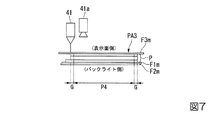
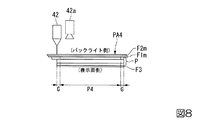
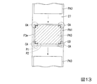
図7および図8に示すように、切断装置41,42は、後述する検出装置で検出された、液晶パネルPと、液晶パネルPに貼合されたシート片FXmと、の貼合面の外周縁に沿って、液晶パネルPに貼合されたシート片FXmを無端状に切断する。表示領域P4の外側には、液晶パネルPの第一及び第二基板を接合するシール剤等を配置する所定幅の額縁部Gが設けられており、この額縁部Gの幅内で切断装置41,42によるシート片FXmの切断(カットライン:WCL、図6(b)参照)が行われる。
As shown in FIGS. 7 and 8, the
このような、貼合面の外周縁の検出および切断装置による切断は、詳しくは以下のようにして行う。 The detection of the outer peripheral edge of the bonding surface and the cutting by the cutting device are performed in detail as follows.
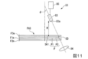
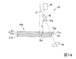
図11は、貼合面の外周縁を検出する第一検出装置(検出装置)81の模式図である。本実施形態のフィルム貼合システム1が備える第一検出装置81は、第三光学部材貼合体PA3における、液晶パネルPと、第三シート片F3mとの貼合面(以下、第一貼合面(貼合面)SA1と称することがある。)の外周縁EDの画像を撮像する撮像装置83と、外周縁EDを照明する照明光源84と、撮像装置83で撮像した画像の記憶や、画像に基づいて外周縁EDを検出するための演算を行う制御部85と、を有する。
FIG. 11 is a schematic diagram of a first detection device (detection device) 81 that detects the outer periphery of the bonding surface. The
このような第一検出装置81は、図1における第一切断装置41のパネル搬送上流側であって、コンベヤ27の始発位置27aと第一切断位置27cとの間に設けられている。
Such a
撮像装置83は、外周縁EDよりも第一貼合面SA1の内側に固定して配置されており、第一貼合面SA1の法線と、撮像装置83の撮像面83aの法線とが、角度θ(以下、撮像装置83の傾斜角度θと称する)をなすように傾斜した姿勢となっている。撮像装置83は、撮像面83aを外周縁EDに向け、第三光学部材貼合体PA3において第三シート片F1mが貼合された側から外周縁EDの画像を撮像する。
The
撮像装置83の傾斜角度θは、第一貼合面SA1をなす第二基板P2の外周縁を確実に撮像できるように設定することが好ましい。例えば、液晶パネルPが、マザーパネルを複数枚の液晶パネルに分割する、いわゆる多面取りで形成されている場合、液晶パネルPを構成する第一基板P1と第二基板P2との外周縁にずれが生じ、第一基板P1の端面が第二基板P2の端面よりも外側にずれることがある。このような場合、撮像装置83の傾斜角度θは、撮像装置83の撮像視野内に第一基板P1の外周縁が入り込まないように設定することが好ましい。
The inclination angle θ of the
このような場合、撮像装置83の傾斜角度θは、第一貼合面SA1と撮像装置83の撮像面83aの中心との間の距離H(以下、撮像装置83の高さHと称する)に適合するように設定されることが好ましい。例えば、撮像装置83の高さHが50mm以上100mm以下の場合、撮像装置83の傾斜角度θは、5°以上20°以下の範囲の角度に設定されることが好ましい。ただし、経験的にずれ量が分かっている場合には、そのずれ量に基づいて撮像装置83の高さH及び撮像装置83の傾斜角度θを求めることができる。本実施形態では、撮像装置83の高さHが78mm、撮像装置83の傾斜角度θが10°に設定されている。
In such a case, the inclination angle θ of the
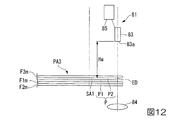
撮像装置83の傾斜角度θは、0°であってもよい。図12は、第一検出装置81の変形例を示す模式図であり、撮像装置83の傾斜角度θが0°である場合の例である。この場合、撮像装置83及び照明光源84の各々が、第一貼合面SA1の法線方向に沿って外周縁EDに重なる位置に配置されていてもよい。
The inclination angle θ of the
第一貼合面SA1と撮像装置83の撮像面83aの中心との間の距離H1(以下、撮像装置83の高さH1と称する)は、第一貼合面SA1の外周縁EDを検出しやすい位置に設定されることが好ましい。例えば、撮像装置83の高さH1は、50mm以上150mm以下の範囲に設定されることが好ましい。
A distance H1 between the first bonding surface SA1 and the center of the
照明光源84は、第三光学部材貼合体PA3における第三シート片F3mが貼合された側とは反対側に固定して配置されている。照明光源84は、外周縁EDよりも第一貼合面SA1の外側に配置されている。本実施形態では、照明光源84の光軸と撮像装置83の撮像面83aの法線とが平行になっている。
The
なお、照明光源84は、第三光学部材貼合体PA3における第三シート片F3mが貼合された側(すなわち、撮像装置83と同じ側)に配置されていてもよい。
In addition, the
また、照明光源84から射出される照明光により、撮像装置83が撮像する外周縁EDが照明されていれば、照明光源84の光軸と撮像装置83の撮像面83aの法線とが交差していてもよい。
If the outer peripheral edge ED imaged by the
図13は、貼合面の外周縁を検出する位置を示す平面図である。図に示す第三光学部材貼合体PA3の搬送経路上(コンベヤ27による搬送経路上)には、検査領域CAが設定されている。検査領域CAは、搬送される第三光学部材貼合体PA3における、第一貼合面SA1の外周縁EDに対応する位置に設定されている。図では、検査領域CAは、平面視矩形の第一貼合面SA1の4つの角部に対応する4箇所に設定されており、第一貼合面SA1の角部を外周縁EDとして検出する構成となっている。図では、第一貼合面SA1の外周縁のうち、角部に対応する鉤状の部分を外周縁EDとして示している。 FIG. 13 is a plan view showing a position where the outer peripheral edge of the bonding surface is detected. Inspection area | region CA is set on the conveyance path | route (on the conveyance path | route by the conveyor 27) of 3rd optical member bonding body PA3 shown to a figure. Inspection area | region CA is set in the position corresponding to outer periphery ED of 1st bonding surface SA1 in 3rd optical member bonding body PA3 conveyed. In the figure, the inspection area CA is set at four locations corresponding to the four corners of the first bonding surface SA1 that is rectangular in plan view, and the corners of the first bonding surface SA1 are detected as the outer peripheral edge ED. It has a configuration. In the figure, among the outer peripheral edges of the first bonding surface SA1, the hook-shaped part corresponding to the corner is shown as the outer peripheral edge ED.
図11の第一検出装置81は、4箇所の検査領域CAにおいて外周縁EDを検出する。具体的には、各検査領域CAには、それぞれ撮像装置83および照明光源84が配置されており、第一検出装置81は、搬送される液晶パネルPごとに第一貼合面SA1の角部を撮像し、撮像データに基づいて外周縁EDを検出する。検出された外周縁EDのデータは、図11に示す制御部85に記憶される。
The
なお、第一貼合面SA1の外周縁が検出可能であれば、検査領域CAの設定位置はこれに限らない。例えば、各検査領域CAが、第一貼合面SA1の各辺の一部(例えば各辺の中央部)に対応する位置に配置されていてもよい。この場合、第一貼合面SA1の各辺(四辺)を外周縁として検出する構成となる。 In addition, if the outer periphery of 1st bonding surface SA1 is detectable, the setting position of test | inspection area | region CA is not restricted to this. For example, each inspection area | region CA may be arrange | positioned in the position corresponding to a part (for example, center part of each side) of each edge | side of 1st bonding surface SA1. In this case, each side (four sides) of the first bonding surface SA1 is detected as an outer peripheral edge.
また、撮像装置83および照明光源84は、各検査領域CAに配置されている構成に限らず、第一貼合面SA1の外周縁EDに沿うように設定された移動経路を移動可能である構成であってもよい。この場合、撮像装置83と照明光源84とが各検査領域CAに位置した際に外周縁EDを検出する構成とすることで、撮像装置83と照明光源84とがそれぞれ1つずつ設けられていれば、外周縁EDの検出が可能となる。
In addition, the
第一切断装置41による第三シート片F3mについてのカット位置は、第一貼合面SA1の外周縁EDの検出結果に基づいて設定される。
The cutting position about the 3rd sheet piece F3m by the
例えば、図11に示す制御部85が、記憶された第一貼合面SA1の外周縁EDのデータに基づいて、形成される第三光学部材F13が液晶パネルPの外側(第一貼合面SA1の外側)にはみ出さない大きさとなるように第三シート片F3mのカット位置を設定する構成とすることができる。また、カット位置の設定は、必ずしも第一検出装置81の制御部85で行う必要はなく、第一検出装置81で検出した外周縁EDのデータを用い、別途計算手段を用いて行うこととしても構わない。
For example, the
第一切断装置41は、制御部85によって設定されたカット位置において第三シート片F3mを切断する。
The
図1に戻り、第一切断装置41は、液晶パネルPに貼合された第三シート片F3mのうち第一貼合面SA1に対応する部分と、その外側の余剰部分とを、検出された外周縁EDに基づいて設定されたカット位置に沿って切り離し、第一貼合面SA1に対応する大きさの第三光学部材F13(図3参照)を切り出す。これにより、液晶パネルPの表裏他方の面に第三光学部材F13が貼合され、且つ、液晶パネルPの表裏一方の面に第一シート片F1mおよび第二シート片F2mが貼合されてなる第四光学部材貼合体PA4が形成される。
Returning to FIG. 1, the
ここで、「第一貼合面SA1に対応する部分」とは、第三シート片F3mにおいて、対向する液晶パネルPの表示領域の大きさ以上、液晶パネルPの外形状(平面視における輪郭形状)の大きさ以下の領域であって、かつ液晶パネルPにおける電気部品取付部等の機能部分を避けた領域を指す。 Here, the “part corresponding to the first bonding surface SA1” means that the outer shape of the liquid crystal panel P (contour shape in plan view) is not less than the size of the display area of the liquid crystal panel P facing the third sheet piece F3m. ) And a region that avoids a functional part such as an electric component mounting portion in the liquid crystal panel P.
本実施形態では、平面視矩形状の液晶パネルPにおける機能部分を除いた三辺では、液晶パネルPの外周縁に沿って余剰部分をレーザーカットし、機能部分に相当する一辺では、液晶パネルPの外周縁から表示領域P4側に適宜入り込んだ位置で余剰部分をレーザーカットする構成を採用できる。例えば、第1基板P1がTFT基板の場合、機能部分に相当する一辺では機能部分を除くよう液晶パネルPの外周縁から表示領域P4側に所定量ずれた位置でカットする構成を採用できる。 In the present embodiment, the surplus portion is laser-cut along the outer peripheral edge of the liquid crystal panel P at three sides excluding the functional portion in the liquid crystal panel P having a rectangular shape in plan view, and the liquid crystal panel P at one side corresponding to the functional portion. It is possible to adopt a configuration in which the surplus portion is laser-cut at a position that appropriately enters the display region P4 side from the outer peripheral edge. For example, when the first substrate P1 is a TFT substrate, it is possible to adopt a configuration in which a cut is made at a position shifted by a predetermined amount from the outer peripheral edge of the liquid crystal panel P toward the display region P4 so as to exclude the functional portion on one side corresponding to the functional portion.
また、予め液晶パネルPにおける機能部分を避けた領域に第三シート片F3mを貼合し、その後、平面視矩形状の液晶パネルPにおける機能部分を除いた三辺において、液晶パネルPの外周縁に沿って余剰部分をレーザーカットしてもよい。 In addition, the third sheet piece F3m is pasted in a region avoiding the functional part in the liquid crystal panel P in advance, and then the outer periphery of the liquid crystal panel P on the three sides excluding the functional part in the liquid crystal panel P having a rectangular shape in plan view. The excess portion may be laser cut along the line.
図14は、貼合面の外周縁を検出する第二検出装置82の模式図である。本実施形態のフィルム貼合システム1が備える第二検出装置82は、第四光学部材貼合体PA4における、液晶パネルPと、第一シート片F1mおよび第二シート片F2mの積層体と、の貼合面(以下、第二貼合面(貼合面)SA2と称することがある。)の外周縁EDの画像を撮像する撮像装置83と、外周縁EDを照明する照明光源84と、撮像装置83で撮像した画像を記憶し、画像に基づいて外周縁EDを検出するための演算を行う制御部85と、を有する。第二検出装置82は、上述の第一検出装置81と同様の構成を有している。
FIG. 14 is a schematic diagram of the
このような第二検出装置82は、図1における第二切断装置42のパネル搬送上流側であって、コンベヤ28の始発位置28aと第二切断位置28bとの間に設けられている。第二検出装置82は、第四光学部材貼合体PA4の搬送経路上において設定された検査領域において、上述の第一検出装置81と同様にして第二貼合面SA2の外周縁EDを検出する。
Such a
第二切断装置42による第一シート片F1mおよび第二シート片F2mの積層体のカット位置は、第二貼合面SA2の外周縁EDの検出結果に基づいて設定される。
The cut position of the laminated body of the first sheet piece F1m and the second sheet piece F2m by the
例えば、図14に示す制御部85は、記憶された第二貼合面SA2の外周縁EDのデータに基づいて、形成される第一光学部材F11および第二光学部材F12が液晶パネルPの外側(第二貼合面SA2の外側)にはみ出さない大きさとなるように、第一シート片F1mおよび第二シート片F2mの積層体のカット位置を設定する構成とすることができる。また、カット位置の設定は、必ずしも第二検出装置82の制御部85で行う必要はなく、第二検出装置82で検出した外周縁EDのデータを用い、別途計算手段を用いて行うこととしても構わない。
For example, the
第二切断装置42は、制御部85によって設定されたカット位置において第一シート片F1mおよび第二シート片F2mの積層体を切断する。
The
第二切断装置42は、液晶パネルPに貼合された第一シート片F1mおよび第二シート片F2mの積層体のうち、第二貼合面SA2に対応する部分と、その外側の余剰部分とを、検出された外周縁EDに沿って切り離し、第二貼合面SA2に対応する大きさの第一光学部材F11および第二光学部材F12(図3参照)を切り出す。
The
ここで、「第二貼合面SA2に対応する部分」とは、第一シート片F1mおよび第二シート片F2mの積層体において、対向する液晶パネルPの表示領域の大きさ以上、液晶パネルPの外形状(平面視における輪郭形状)の大きさ以下の領域であって、かつ液晶パネルPにおける電気部品取付部等の機能部分を避けた領域を指す。 Here, the “part corresponding to the second bonding surface SA2” means the liquid crystal panel P that is equal to or larger than the size of the display area of the opposing liquid crystal panel P in the laminate of the first sheet piece F1m and the second sheet piece F2m. Is an area that is equal to or less than the size of the outer shape (contour shape in plan view) and that avoids a functional part such as an electrical component mounting portion in the liquid crystal panel P.
以上の操作により、液晶パネルPの表裏他方の面に第三光学部材F13が貼合され、且つ、液晶パネルPの表裏一方の面に第一光学部材F11および第二光学部材F12が貼合されてなる第五光学部材貼合体が形成される。 By the above operation, the third optical member F13 is bonded to the other surface of the liquid crystal panel P, and the first optical member F11 and the second optical member F12 are bonded to the front and back surfaces of the liquid crystal panel P. A fifth optical member bonded body is formed.
以上説明したように、上記実施形態におけるフィルム貼合システム1は、液晶パネルPの表裏両面に液晶パネルPの表示領域P4よりも大きい光学部材シートFXのシート片FXmをそれぞれ貼合する貼合装置13,15,18と、液晶パネルPの表裏両面にそれぞれ貼合されたシート片FXmから、液晶パネルPとシート片FXmとの貼合面に対応する部分の外側に配置された余剰部分を切り離し、液晶パネルPとシート片FXmとの貼合面に対応する大きさの光学部材F1Xを液晶パネルPの表裏両面にそれぞれ形成する切断装置41,42と、を備えている。そのため、光学部材F1Xを表示領域P4の際まで精度よく設けることが可能となり、表示領域P4外側の額縁部G(図3参照)を狭めて表示エリアの拡大及び機器の小型化が図られる。
As explained above, the
また、上記フィルム貼合システム1は、光学部材シートFXの光学軸方向の検査データに基づき、液晶パネルPとシート片FXmとの相対貼合位置を決定する制御装置25を備え、貼合装置13,15,18は、制御装置25が決定した相対貼合位置に基づき、シート片FXmを液晶パネルPに貼合する。そのため、光学部材シートFXの面内において光学軸方向にばらつきが存在する場合でも、その光学軸方向のばらつきに応じて、シート片FXmと液晶パネルPとの相対貼合位置を適切に調整することができる。これにより、液晶パネルPに対する光学部材F1Xの光学軸方向の精度を向上させることができ、光学表示デバイスの精彩及びコントラストを高めることができる。
Moreover, the said
また、上記フィルム貼合システム1においては、貼合装置13,15,18は、光学部材シートFXを原反ロールR1からセパレータシートF3aと共に巻き出す巻き出し部31aと、光学部材シートFXをセパレータシートF3aを残してカットしてシート片FXmとするカット部31bと、シート片FXmをセパレータシートF3aから剥離させるナイフエッジ31cと、シート片FXmを保持面32aに貼り付けて保持すると共に、保持面32aに保持したシート片FXmを液晶パネルPに貼合する貼合ヘッド32と、を有する。そのため、シート片FXmの連続的な貼合が容易になり、光学表示デバイスの生産効率を高めることができる。また、貼合ヘッド32として円弧状の保持面32aを有するものを用いているため、円弧状の保持面32aの傾動によりシート片FXmをスムーズに保持できると共に、同じく円弧状の保持面32aの傾動によりシート片FXmを液晶パネルPに確実に貼合することができる。
Moreover, in the said
また、上記フィルム貼合システム1においては、第一切断装置41および第二切断装置42は、レーザーカッターであり、第一切断装置41および第二切断装置42は、同一のレーザー出力装置40に接続されており、レーザー出力装置40から出力されたレーザーが第一切断装置41および第二切断装置42に分岐されて供給される。そのため、第一切断装置41と第二切断装置42のそれぞれに別々のレーザー出力装置を接続する場合に比べて、光学表示デバイスの生産システムの小型化を図ることができる。
In the
[第二実施形態]
図9は、第二実施形態のフィルム貼合システムに適用される貼合装置の模式図である。
図9(a)は、シート片FXmを貼合ヘッド60に保持した状態を示す図であり、図9(b)は、シート片FXmを液晶パネルPに貼合した状態を示す図である。
[Second Embodiment]
Drawing 9 is a mimetic diagram of a pasting device applied to a film pasting system of a second embodiment.
FIG. 9A is a diagram illustrating a state in which the sheet piece FXm is held by the
本実施形態において第一実施形態と異なる点は、第一実施形態の貼合装置が円弧状の保持面32aを有する貼合ヘッド32を用いたのに対し、本実施形態の貼合装置が平面状の保持面60aを有する貼合ヘッド60を用いている点である。よって、ここでは、貼合ヘッド60の構成を中心に説明し、第一実施形態と共通する構成要素については、同じ符号を付し、詳細な説明は省略する。
In this embodiment, the difference from the first embodiment is that the bonding apparatus of the first embodiment uses a
本実施形態の貼合装置は、貼合ヘッド60と、貼合ローラ62と、貼合ヘッド60および貼合ローラ62を支持するガイドバー61と、ガイドバー61を液晶パネルPに対して傾動させた状態で水平移動させる駆動装置63と、を有する。図示はしないが、本実施形態の貼合装置には、図5に示したものと同様の巻き出し部、カット部およびナイフエッジ(剥離部)が設けられている。
The bonding apparatus of the present embodiment tilts the
貼合ヘッド60は、セパレータシートから剥離されたシート片FXmを保持する平面状の保持面60aを有する。保持面60aは、ガイドバー61が傾動することにより、液晶パネルPに対して傾斜する。シート片FXmは、その一端部が保持面60aの外側にはみ出すように位置決めされ、保持面60aに吸着される。シート片FXmの吸着力は弱く、シート片FXmは保持面60aに保持された状態で、保持面60a上を滑るようにして水平方向に移動することができる。
The
貼合ローラ62は、貼合ヘッド60の側方に配置され、貼合ヘッド60の保持面60aからはみ出したシート片FXmを液晶パネルPに押し付けて貼着する。この状態で駆動装置63によりガイドバー61を水平方向に移動させると、シート片FXmの前記一端部が液晶パネルPに貼着された状態で貼合ヘッド60および貼合ローラ62がシート片FXmの前記一端部側から他端部側に向けて水平移動する。これにより、シート片FXmが貼合ローラ62によって一端部側から徐々に液晶パネルPに貼合される。
The laminating
貼合ヘッド60は、保持面60aに保持したシート片FXmを、水平方向でヘッド移動方向及びその直交方向並びに回転方向でアライメントする。シート片FXmと液晶パネルPとの貼合位置(相対貼合位置)は、第一実施形態と同様に、光学部材シートFXの光学軸方向の検査データに基づいて制御装置25(図1参照)が決定する。貼合ヘッド60は、制御装置25が決定した相対貼合位置に基づき、保持面60aに保持したシート片FXmを液晶パネルPに貼合する。
The
よって、本実施形態においても、表示領域周辺の額縁部を縮小して表示エリアの拡大及び機器の小型化を図ることができる光学表示デバイスの生産システムが提供できる。 Therefore, also in the present embodiment, it is possible to provide an optical display device production system that can reduce the frame portion around the display area to enlarge the display area and downsize the device.
[第一変形形態]
上記実施形態では、切断装置41,42の一例としてCO2レーザーを用いたが、切断装置41,42はこれに限定されない。切断刃などの他の切断手段を切断装置41,42として用いることも可能である。
[First variant]
In the above embodiment, the CO 2 laser as an example of a
例えば、図10に示すように、第一基板P1がその外周縁の三辺を第二基板P2の対応する三辺に沿わせると共に、外周縁の残りの一辺を第二基板P2の対応する一辺よりも外側に張り出させるように形成されている場合には、第二基板P2の大きさは表示領域P4の大きさと概ね一致するため、切断刃を第二基板P2の外周に沿って移動させれば、第二基板P2に接合されたシート片F3mを、液晶パネルPとシート片F3mとの貼合面に対応する大きさの光学部材F13として形成することができる。 For example, as shown in FIG. 10, the first substrate P1 has three sides of the outer periphery thereof along the corresponding three sides of the second substrate P2, and the other side of the outer periphery is a corresponding side of the second substrate P2. When the second substrate P2 is formed so as to protrude outward, the size of the second substrate P2 substantially matches the size of the display region P4, so the cutting blade is moved along the outer periphery of the second substrate P2. Then, the sheet piece F3m bonded to the second substrate P2 can be formed as an optical member F13 having a size corresponding to the bonding surface of the liquid crystal panel P and the sheet piece F3m.
この場合、シート片F3mの余剰部分は液晶パネルPに対して面で接着される部分が殆どなく、光学部材F13とその周辺の余剰部分とは概ね粘着層F2aの粘着力のみによって接着される。そのため、シート片F3mの余剰部分を液晶パネルPから剥離し回収する装置も余剰部分の端部をつまんで引っ張るだけの簡単な構成でよく、装置構成が簡単になる。また、上記実施形態では、シート片F1m,F2mの余剰部分とシート片F3mの余剰部分とを別々の工程で液晶パネルPから剥離し回収したが、シート片F3mの余剰部分の回収が非常に容易であることから、シート片F1m,F2mの余剰部分を液晶パネルPから剥離し回収する際にシート片F3mの余剰部分をまとめて液晶パネルPから剥離し回収することも可能となる。その場合、余剰部分の剥離装置を2箇所に設ける必要がないので、光学表示デバイスの生産システムを小型化することができる。 In this case, the surplus portion of the sheet piece F3m has almost no portion to be bonded to the liquid crystal panel P on the surface, and the optical member F13 and the surplus portion around the optical member F13 are bonded only by the adhesive force of the adhesive layer F2a. Therefore, the apparatus for peeling off and recovering the surplus portion of the sheet piece F3m from the liquid crystal panel P may have a simple configuration by simply pinching and pulling the end portion of the surplus portion, thereby simplifying the apparatus configuration. Moreover, in the said embodiment, although the excess part of the sheet piece F1m and F2m and the excess part of the sheet piece F3m were peeled off and collect | recovered from the liquid crystal panel P by the separate process, collection | recovery of the excess part of the sheet piece F3m is very easy. Therefore, when the excess portions of the sheet pieces F1m and F2m are peeled off and collected from the liquid crystal panel P, the surplus portions of the sheet pieces F3m can be peeled from the liquid crystal panel P and collected together. In that case, since it is not necessary to provide the surplus part peeling apparatus in two places, the production system of an optical display device can be reduced in size.
[第二変形形態]
上記実施形態では、液晶パネルPに対するシート片FXmの貼合位置(相対貼合位置)の決定方法として、光学部材シートFXの面内の平均的な光学軸の方向を用いる方法を説明した。上記実施形態では、光学部材シートFXの面内の最大ずれ角θmaxと最小ずれ角θminとの平均値θmidを平均ずれ角とした場合に、光学部材シートFXのエッジラインに対して平均ずれ角θmidをなす方向を光学部材シートFXの面内の平均的な光学軸の方向として検出したが、光学部材シートFXの面内の平均的な光学軸の方向の検出方法はこれに限定されない。
[Second variation]
In the said embodiment, the method of using the direction of the average optical axis in the surface of the optical member sheet | seat FX as a determination method of the bonding position (relative bonding position) of the sheet piece FXm with respect to liquid crystal panel P was demonstrated. In the above embodiment, the average deviation angle θmid with respect to the edge line of the optical member sheet FX when the average deviation θmid between the in-plane maximum deviation angle θmax and the minimum deviation angle θmin is the average deviation angle. Is detected as the direction of the average optical axis in the plane of the optical member sheet FX, but the method for detecting the direction of the average optical axis in the plane of the optical member sheet FX is not limited to this.
例えば、光学部材シートFXの幅方向に設定された複数の検査ポイントCP(図6(a)参照)の中から一または複数の検査ポイントCPを選択し、選択された検査ポイントCP毎に、光学軸の方向と光学部材シートFXのエッジラインELとのなす角度(ずれ角)を検出する。そして、選択された一または複数の検査ポイントCPの光学軸方向のずれ角の平均値を平均ずれ角として検出し、光学部材シートFXのエッジラインELに対して前記平均ずれ角をなす方向を光学部材シートFXの平均的な光学軸の方向として検出してもよい。 For example, one or a plurality of inspection points CP are selected from a plurality of inspection points CP (see FIG. 6A) set in the width direction of the optical member sheet FX, and an optical is selected for each selected inspection point CP. An angle (deviation angle) formed between the axis direction and the edge line EL of the optical member sheet FX is detected. Then, the average value of the deviation angles in the optical axis direction of the selected one or more inspection points CP is detected as the average deviation angle, and the direction forming the average deviation angle with respect to the edge line EL of the optical member sheet FX is optically detected. You may detect as the direction of the average optical axis of member sheet FX.
[第三変形形態]
上記実施形態では、液晶パネルPにシート片FXmを貼合する方法として貼合ヘッド32,60を用いる方法を説明したが、本発明はこれに限定されない。貼合ヘッド32,60を介さずに、ナイフエッジ31cでセパレータシートF3aから剥離されたシート片FXmを貼合ロールなどで直接液晶パネルPに貼合する方法を用いてもよい。
[Third variant]
In the said embodiment, although the method using the bonding heads 32 and 60 was demonstrated as a method of bonding the sheet piece FXm to liquid crystal panel P, this invention is not limited to this. You may use the method of bonding the sheet | seat piece FXm peeled from the separator sheet F3a with the
上記実施形態のフィルム貼合システム1では、検出装置を用いて複数の液晶パネルPごとに貼合面の外周縁を検出し、検出した外周縁に基づいて、個々の液晶パネルPごとに貼合したシート片FXmの切断位置を設定する。これにより、液晶パネルPやシート片FXmの大きさの個体差によらず所望の大きさの光学部材を切り離すことができるため、液晶パネルPやシート片FXmの大きさの個体差による品質バラツキをなくし、表示領域周辺の額縁部を縮小して表示エリアの拡大及び機器の小型化を図ることができる。
In the
1…フィルム貼合システム(光学表示デバイスの生産システム)、13…第一貼合装置(貼合手段)、15…第二貼合装置(貼合手段)、18…第三貼合装置(貼合手段)、25…制御装置、31…シート搬送装置、31a…巻き出し部、31b…カット部、31c…ナイフエッジ(剥離部)、32…貼合ヘッド、32a…保持面、40…切断手段、41…第一切断装置(切断手段)、42…第二切断装置(切断手段)、43…レーザー出力装置、60…貼合ヘッド、60a…保持面、81…第一検出装置(検出装置)、82…第二検出装置(検出装置)、P…液晶パネル(光学表示部品)、P4…表示領域、F1…第一光学部材シート(光学部材シート)、F2…第二光学部材シート(光学部材シート)、F3…第三光学部材シート(光学部材シート)、FX…光学部材シート、F3a…セパレータシート、F11…第一光学部材(光学部材)、F12…第二光学部材(光学部材)、F13…第三光学部材(光学部材)、F1X…光学部材、F1m…第一シート片、F2m…第二シート片、F3m…第三シート片、FXm…シート片、R1…原反ロール、PA3…第三光学部品貼合体(貼合体)、PA4…第四光学部品貼合体(貼合体)、ED…第一貼合面の外周縁、第二貼合面の外周縁、SA1…第一貼合面(貼合面)、SA2…第二貼合面(貼合面)
DESCRIPTION OF
Claims (5)
前記光学表示部品の表裏両面に前記光学表示部品の表示領域よりも大きい光学部材シートのシート片をそれぞれ貼合して貼合体とする貼合手段と、
前記貼合体において、前記シート片と前記光学表示部品との貼合面の外周縁を検出する検出装置と、
前記貼合体において、前記光学表示部品の表裏両面にそれぞれ貼合された前記シート片から前記貼合面に対応する部分の外側に配置された余剰部分を、前記外周縁に沿って切り離し、前記貼合面に対応する大きさの前記光学部材を前記光学表示部品の表裏両面にそれぞれ形成する切断手段と、を備えている光学表示デバイスの生産システム。 An optical display device production system in which an optical member is bonded to an optical display component,
Bonding means for bonding a sheet piece of an optical member sheet larger than the display area of the optical display component on both front and back surfaces of the optical display component, respectively,
In the bonding body, a detection device for detecting an outer peripheral edge of a bonding surface between the sheet piece and the optical display component;
In the bonded body, an excess portion disposed outside the portion corresponding to the bonding surface is cut off from the sheet pieces bonded to the front and back surfaces of the optical display component along the outer peripheral edge, and the bonding is performed. An optical display device production system comprising: cutting means for forming the optical member having a size corresponding to the mating surface on both front and back surfaces of the optical display component.
前記貼合手段は、前記制御装置が決定した相対貼合位置に基づき、前記シート片を前記光学表示部品に貼合する請求項1に記載の光学表示デバイスの生産システム。 Based on inspection data in the optical axis direction of the optical member sheet, comprising a control device for determining a relative bonding position between the optical display component and the sheet piece,
2. The optical display device production system according to claim 1, wherein the bonding unit bonds the sheet piece to the optical display component based on a relative bonding position determined by the control device.
前記第一切断装置および前記第二切断装置は、レーザーカッターであり、
前記第一切断装置および前記第二切断装置は、同一のレーザー出力装置に接続されており、前記レーザー出力装置から出力されたレーザーが前記第一切断装置および前記第二切断装置に分岐されて供給される請求項1から4の何れか一項に記載の光学表示デバイスの生産システム。 The cutting means includes a first cutting device that separates the surplus portion from a sheet piece bonded to one surface of the optical display component, and a sheet piece bonded to the other surface of the optical display component. A second cutting device for cutting off the surplus part,
The first cutting device and the second cutting device are laser cutters,
The first cutting device and the second cutting device are connected to the same laser output device, and the laser output from the laser output device is branched and supplied to the first cutting device and the second cutting device An optical display device production system according to any one of claims 1 to 4.
Priority Applications (3)
| Application Number | Priority Date | Filing Date | Title |
|---|---|---|---|
| JP2013105589A JP6193618B2 (en) | 2013-05-17 | 2013-05-17 | Optical display device production system |
| TW103117260A TW201506491A (en) | 2013-05-17 | 2014-05-16 | Production system for optical display device |
| PCT/JP2014/063048 WO2014185513A1 (en) | 2013-05-17 | 2014-05-16 | Optical display device production system |
Applications Claiming Priority (1)
| Application Number | Priority Date | Filing Date | Title |
|---|---|---|---|
| JP2013105589A JP6193618B2 (en) | 2013-05-17 | 2013-05-17 | Optical display device production system |
Publications (2)
| Publication Number | Publication Date |
|---|---|
| JP2014228564A true JP2014228564A (en) | 2014-12-08 |
| JP6193618B2 JP6193618B2 (en) | 2017-09-06 |
Family
ID=51898488
Family Applications (1)
| Application Number | Title | Priority Date | Filing Date |
|---|---|---|---|
| JP2013105589A Active JP6193618B2 (en) | 2013-05-17 | 2013-05-17 | Optical display device production system |
Country Status (3)
| Country | Link |
|---|---|
| JP (1) | JP6193618B2 (en) |
| TW (1) | TW201506491A (en) |
| WO (1) | WO2014185513A1 (en) |
Citations (6)
| Publication number | Priority date | Publication date | Assignee | Title |
|---|---|---|---|---|
| JPH0887007A (en) * | 1994-09-19 | 1996-04-02 | Ookubo Seisakusho:Kk | Sticking device for polarizing plate |
| JP2005043384A (en) * | 2002-07-04 | 2005-02-17 | Fuji Photo Film Co Ltd | Method and apparatus for sticking polarizing plate |
| WO2006129523A1 (en) * | 2005-05-30 | 2006-12-07 | Sharp Kabushiki Kaisha | Liquid crystal display device manufacturing method and liquid crystal display device manufacturing device |
| JP2007288010A (en) * | 2006-04-19 | 2007-11-01 | Lintec Corp | Sheet cutting device and cutting method |
| JP2012247714A (en) * | 2011-05-30 | 2012-12-13 | V Technology Co Ltd | Device for sticking optical film to substrate |
| JP2016013557A (en) * | 2013-02-13 | 2016-01-28 | 住友化学株式会社 | Laser light irradiation apparatus and optical member bonding body manufacturing apparatus |
-
2013
- 2013-05-17 JP JP2013105589A patent/JP6193618B2/en active Active
-
2014
- 2014-05-16 TW TW103117260A patent/TW201506491A/en unknown
- 2014-05-16 WO PCT/JP2014/063048 patent/WO2014185513A1/en not_active Ceased
Patent Citations (6)
| Publication number | Priority date | Publication date | Assignee | Title |
|---|---|---|---|---|
| JPH0887007A (en) * | 1994-09-19 | 1996-04-02 | Ookubo Seisakusho:Kk | Sticking device for polarizing plate |
| JP2005043384A (en) * | 2002-07-04 | 2005-02-17 | Fuji Photo Film Co Ltd | Method and apparatus for sticking polarizing plate |
| WO2006129523A1 (en) * | 2005-05-30 | 2006-12-07 | Sharp Kabushiki Kaisha | Liquid crystal display device manufacturing method and liquid crystal display device manufacturing device |
| JP2007288010A (en) * | 2006-04-19 | 2007-11-01 | Lintec Corp | Sheet cutting device and cutting method |
| JP2012247714A (en) * | 2011-05-30 | 2012-12-13 | V Technology Co Ltd | Device for sticking optical film to substrate |
| JP2016013557A (en) * | 2013-02-13 | 2016-01-28 | 住友化学株式会社 | Laser light irradiation apparatus and optical member bonding body manufacturing apparatus |
Also Published As
| Publication number | Publication date |
|---|---|
| WO2014185513A1 (en) | 2014-11-20 |
| TW201506491A (en) | 2015-02-16 |
| JP6193618B2 (en) | 2017-09-06 |
Similar Documents
| Publication | Publication Date | Title |
|---|---|---|
| JP5692712B2 (en) | Optical display device production system | |
| CN104204918B (en) | The production system of optical display means | |
| TWI661928B (en) | Optical display device production system | |
| JP5804404B2 (en) | Optical display device production system and optical display device production method | |
| JP5724147B2 (en) | Optical display device production system | |
| JP6182805B2 (en) | Optical display device production system | |
| KR102110007B1 (en) | System and method for producing optical display devices | |
| WO2014129353A1 (en) | Production system and production method for optical display device | |
| JP6223439B2 (en) | Optical display device production system | |
| JP5618283B2 (en) | Optical display device production system and optical display device production method | |
| JP2014157344A (en) | Production system of optical display device | |
| JP6193618B2 (en) | Optical display device production system |
Legal Events
| Date | Code | Title | Description |
|---|---|---|---|
| A621 | Written request for application examination |
Free format text: JAPANESE INTERMEDIATE CODE: A621 Effective date: 20160502 |
|
| A131 | Notification of reasons for refusal |
Free format text: JAPANESE INTERMEDIATE CODE: A131 Effective date: 20170104 |
|
| A521 | Request for written amendment filed |
Free format text: JAPANESE INTERMEDIATE CODE: A523 Effective date: 20170203 |
|
| TRDD | Decision of grant or rejection written | ||
| A01 | Written decision to grant a patent or to grant a registration (utility model) |
Free format text: JAPANESE INTERMEDIATE CODE: A01 Effective date: 20170801 |
|
| A61 | First payment of annual fees (during grant procedure) |
Free format text: JAPANESE INTERMEDIATE CODE: A61 Effective date: 20170810 |
|
| R150 | Certificate of patent or registration of utility model |
Ref document number: 6193618 Country of ref document: JP Free format text: JAPANESE INTERMEDIATE CODE: R150 |
|
| S531 | Written request for registration of change of domicile |
Free format text: JAPANESE INTERMEDIATE CODE: R313531 |
|
| R350 | Written notification of registration of transfer |
Free format text: JAPANESE INTERMEDIATE CODE: R350 |