JP2014182227A - Optical scanner, image display device, and head-mounted display - Google Patents
Optical scanner, image display device, and head-mounted display Download PDFInfo
- Publication number
- JP2014182227A JP2014182227A JP2013055730A JP2013055730A JP2014182227A JP 2014182227 A JP2014182227 A JP 2014182227A JP 2013055730 A JP2013055730 A JP 2013055730A JP 2013055730 A JP2013055730 A JP 2013055730A JP 2014182227 A JP2014182227 A JP 2014182227A
- Authority
- JP
- Japan
- Prior art keywords
- axis
- shaft portion
- strain detection
- signal
- detection element
- Prior art date
- Legal status (The legal status is an assumption and is not a legal conclusion. Google has not performed a legal analysis and makes no representation as to the accuracy of the status listed.)
- Pending
Links
Images


Classifications
-
- G—PHYSICS
- G02—OPTICS
- G02B—OPTICAL ELEMENTS, SYSTEMS OR APPARATUS
- G02B26/00—Optical devices or arrangements for the control of light using movable or deformable optical elements
- G02B26/08—Optical devices or arrangements for the control of light using movable or deformable optical elements for controlling the direction of light
- G02B26/10—Scanning systems
- G02B26/101—Scanning systems with both horizontal and vertical deflecting means, e.g. raster or XY scanners
-
- G—PHYSICS
- G02—OPTICS
- G02B—OPTICAL ELEMENTS, SYSTEMS OR APPARATUS
- G02B26/00—Optical devices or arrangements for the control of light using movable or deformable optical elements
- G02B26/08—Optical devices or arrangements for the control of light using movable or deformable optical elements for controlling the direction of light
- G02B26/0816—Optical devices or arrangements for the control of light using movable or deformable optical elements for controlling the direction of light by means of one or more reflecting elements
- G02B26/0833—Optical devices or arrangements for the control of light using movable or deformable optical elements for controlling the direction of light by means of one or more reflecting elements the reflecting element being a micromechanical device, e.g. a MEMS mirror, DMD
- G02B26/085—Optical devices or arrangements for the control of light using movable or deformable optical elements for controlling the direction of light by means of one or more reflecting elements the reflecting element being a micromechanical device, e.g. a MEMS mirror, DMD the reflecting means being moved or deformed by electromagnetic means
Abstract
Description
本発明は、光スキャナー、画像表示装置およびヘッドマウントディスプレイに関するものである。 The present invention relates to an optical scanner, an image display device, and a head mounted display.
例えば、プロジェクター、ヘッドマウントディスプレイ等に用いられ、光を2次元的に走査する光スキャナーが知られている(例えば、特許文献1参照)。
例えば、特許文献1に記載の光スキャナーは、枠状の外側フレーム(固定部)と、外側フレームの内側に設けられた枠状の内側フレーム(枠体部)と、内側フレームを外側フレームに対して回動可能に支持する1対の第2の弾性ビーム(第2軸部)と、内側フレームの内側に設けられたミラー部(可動部)と、ミラー部を内側フレームに対して回動可能に支持する1対の第1の弾性ビーム(第1軸部)とを有する。
For example, an optical scanner that is used in a projector, a head-mounted display, or the like and scans light in a two-dimensional manner is known (for example, see Patent Document 1).
For example, the optical scanner described in
このような光スキャナーでは、第2の弾性ビームを捩れ変形させながら内側フレームを外側フレームに対して回動させるとともに、第1の弾性ビームを捩れ変形させながらミラー部を内側フレームに対して回動させることにより、ミラー部で反射した光を2次元的に走査する。
また、特許文献1に記載の光スキャナーでは、内側フレームと外側フレームとの間の第2の弾性ビームの外側フレーム側の端部にピエゾ抵抗が配置されている。これにより、このピエゾ抵抗の抵抗値変化に基づいて、第2の弾性ビームの捩れ変形による内側フレームおよびミラー部の回動を検知することができる。
In such an optical scanner, the inner frame is rotated with respect to the outer frame while twisting and deforming the second elastic beam, and the mirror portion is rotated with respect to the inner frame while twisting and deforming the first elastic beam. By doing so, the light reflected by the mirror part is scanned two-dimensionally.
Further, in the optical scanner described in
ピエゾ抵抗には、応力に対する応答感度が温度変化に伴って変化するという温度特性がある。
一方、特許文献1に記載の光スキャナーでは、ピエゾ抵抗が第2の弾性ビームの外側フレーム側の端部に配置されているため、外側フレームを支持して設置したとき、外部からの熱が外部フレームに伝達され、ピエゾ抵抗が外部からの熱の影響を受けやすい。
そのため、ピエゾ抵抗の温度と、第2の弾性ビームの捩れ変形を生じる主たる部分の温度とが異なってしまい、上述したピエゾ抵抗の温度特性に起因して、ピエゾ抵抗の検出精度の低下を招くという問題があった。
本発明の目的は、歪検出素子に対する外部からの熱の影響を抑制しつつ、歪検出素子を用いて可動部の挙動を検出することができる光スキャナーを提供すること、また、かかる光スキャナーを備える信頼性に優れた画像表示装置およびヘッドマウントディスプレイを提供することにある。
The piezoresistor has a temperature characteristic that response sensitivity to stress changes with temperature change.
On the other hand, in the optical scanner described in
Therefore, the temperature of the piezoresistor is different from the temperature of the main part that causes the torsional deformation of the second elastic beam, which causes a decrease in piezoresistor detection accuracy due to the temperature characteristics of the piezoresistor described above. There was a problem.
An object of the present invention is to provide an optical scanner capable of detecting the behavior of a movable part using a strain detection element while suppressing the influence of heat from the outside on the strain detection element, and to provide such an optical scanner. An object of the present invention is to provide an image display device and a head-mounted display that are excellent in reliability.
このような目的は、下記の本発明により達成される。
本発明の光スキャナーは、光反射性を有する光反射部が設けられ、かつ、第1の軸周りに揺動可能な可動部と、
前記第1の軸に交差する第2の軸周りに揺動可能な枠体部と、
前記可動部と前記枠体部とを接続する第1軸部と、
固定部と、
前記枠体部と前記固定部とを接続する第2軸部と、
前記第2軸部の前記枠体部側の端部、または、前記可動部、前記枠体部および前記第1軸部のうちのいずれかに配置された第1歪検出素子と、
前記第2軸部の前記枠体部側の端部、または、前記可動部、前記枠体部および前記第1軸部のうちのいずれかに配置された第2歪検出素子と、
前記第1歪検出素子の検出信号が入力され、前記第2軸部の曲げ変形に基づく信号を出力する第1信号処理部と、
前記第2歪検出素子の検出信号が入力され、前記第2軸部の捩れ変形に基づく信号を出力する第2信号処理部と、を備えることを特徴とする。
Such an object is achieved by the present invention described below.
The optical scanner of the present invention is provided with a light reflecting portion having light reflectivity, and a movable portion that can swing around a first axis;
A frame portion swingable around a second axis intersecting the first axis;
A first shaft portion connecting the movable portion and the frame body portion;
A fixed part;
A second shaft portion connecting the frame body portion and the fixed portion;
A first strain detection element disposed on an end of the second shaft portion on the frame body side, or one of the movable portion, the frame body portion, and the first shaft portion;
An end of the second shaft portion on the side of the frame body portion, or a second strain detection element disposed at any of the movable portion, the frame body portion, and the first shaft portion;
A first signal processing unit that receives a detection signal of the first strain detection element and outputs a signal based on bending deformation of the second shaft portion;
And a second signal processing unit that receives a detection signal of the second strain detection element and outputs a signal based on the torsional deformation of the second shaft portion.
このような光スキャナーによれば、第1信号処理部から出力された信号に基づいて、可動部の第1の軸周りの挙動を検出することができる。また、第2信号処理部から出力された信号に基づいて、可動部の第2の軸周りの挙動を検出することができる。また、第1歪検出素子および第2歪検出素子が第2軸部の枠体部側の端部、または、可動部、枠体部および第1軸部のうちのいずれかに配置されているため、第1歪検出素子および第2歪検出素子に対する外部からの固定部を介した熱の影響を抑制することができる。 According to such an optical scanner, it is possible to detect the behavior of the movable part around the first axis based on the signal output from the first signal processing part. Further, the behavior of the movable part around the second axis can be detected based on the signal output from the second signal processing part. Further, the first strain detection element and the second strain detection element are disposed at the end of the second shaft portion on the frame body side, or at any of the movable portion, the frame body portion, and the first shaft portion. Therefore, it is possible to suppress the influence of heat from the external fixing portion on the first strain detection element and the second strain detection element.
本発明の光スキャナーでは、前記第1歪検出素子は、前記第2軸部の前記枠体部側の端部に配置され、前記第2軸部の変形を検出することが好ましい。
これにより、可動部に入射した光による熱が第1歪検出素子に与える影響を抑制することができる。また、可動部の第1の軸周りの挙動の検出に用いる歪抵抗素子を第1軸部に設ける必要がないため、第1軸部の設計の自由度を高めることができる。
In the optical scanner according to the aspect of the invention, it is preferable that the first strain detection element is disposed at an end portion of the second shaft portion on the frame body portion side to detect deformation of the second shaft portion.
Thereby, the influence which the heat by the light which injected into the movable part has on a 1st distortion | strain detection element can be suppressed. Moreover, since it is not necessary to provide the first shaft portion with a strain resistance element used for detecting the behavior of the movable portion around the first axis, the degree of freedom in designing the first shaft portion can be increased.
本発明の光スキャナーでは、前記第1歪検出素子は、前記第2軸部の長手方向に沿った方向に延びる長手形状をなすピエゾ抵抗領域と、前記ピエゾ抵抗領域上に前記第2軸部の長手方向に沿った方向に並んで配置された1対の端子と、を備えることが好ましい。
これにより、第1歪検出素子から出力される信号に含まれる第2軸部の曲げ変形に基づく信号を大きくすることができる。
In the optical scanner according to the aspect of the invention, the first strain detection element may include a piezoresistive region having a longitudinal shape extending in a direction along the longitudinal direction of the second shaft portion, and the second shaft portion on the piezoresistive region. And a pair of terminals arranged side by side in a direction along the longitudinal direction.
Thereby, the signal based on the bending deformation of the second shaft portion included in the signal output from the first strain detection element can be increased.
本発明の光スキャナーでは、前記第1信号処理部から出力された信号に基づいて、前記可動部の前記第1の軸周りの挙動を検出することが好ましい。
これにより、検出した挙動に基づいて、可動部の第1の軸周りの挙動を所望の状態となるように制御したり、可動部の第1の軸周りの挙動と他の装置の動作とを同期させたりすることができる。
本発明の光スキャナーでは、オブザーバーを用いて、前記第1信号処理部から出力された信号に基づいて、前記可動部の前記第1の軸周りの挙動を推定することが好ましい。
これにより、可動部の第1の軸周りの揺動が共振状態でなくても、第1信号処理部から出力された信号に基づいて、可動部の第1の軸周りの挙動を検出することができる。
In the optical scanner according to the aspect of the invention, it is preferable that the behavior of the movable unit around the first axis is detected based on a signal output from the first signal processing unit.
Thereby, based on the detected behavior, the behavior of the movable part around the first axis is controlled to be in a desired state, or the behavior of the movable part around the first axis and the operation of other devices are controlled. Can be synchronized.
In the optical scanner according to the aspect of the invention, it is preferable that the behavior of the movable part around the first axis is estimated based on a signal output from the first signal processing unit using an observer.
Thereby, even if the swing of the movable part around the first axis is not in the resonance state, the behavior of the movable part around the first axis is detected based on the signal output from the first signal processing part. Can do.
本発明の光スキャナーでは、前記可動部の前記第1の軸周りの揺動に関する共振周波数における振幅と、前記枠体部の前記第1の軸周りの揺動に関する共振周波数における振幅との比を用いて、前記第1信号処理部から出力された信号に基づいて、前記可動部の前記第1の軸周りの挙動を推定することが好ましい。
これにより、比較的簡単な構成で、第1信号処理部から出力された信号に基づいて、可動部の第1の軸周りの挙動を高精度に検出することができる。
In the optical scanner according to the aspect of the invention, the ratio of the amplitude at the resonance frequency related to the oscillation of the movable portion around the first axis to the amplitude at the resonance frequency related to the oscillation of the frame body portion around the first axis is calculated. It is preferable to estimate the behavior of the movable part around the first axis based on the signal output from the first signal processing part.
Thereby, it is possible to detect the behavior of the movable portion around the first axis with high accuracy based on the signal output from the first signal processing portion with a relatively simple configuration.
本発明の光スキャナーでは、前記第2歪検出素子は、前記第2軸部の前記枠体部側の端部に配置され、前記第2軸部の変形を検出することが好ましい。
これにより、可動部に入射した光による熱が第2歪検出素子に与える影響を抑制することができる。また、可動部の第2の軸周りの挙動の検出に用いる歪抵抗素子を第1軸部に設ける必要がないため、第1軸部の設計の自由度を高めることができる。
In the optical scanner according to the aspect of the invention, it is preferable that the second strain detection element is disposed at an end portion of the second shaft portion on the frame body portion side to detect deformation of the second shaft portion.
Thereby, the influence which the heat by the light which injected into the movable part has on a 2nd distortion | strain detection element can be suppressed. In addition, since it is not necessary to provide the first shaft portion with a strain resistance element used for detecting the behavior of the movable portion around the second axis, the degree of freedom in designing the first shaft portion can be increased.
本発明の光スキャナーでは、前記第2信号処理部から出力された信号に基づいて、前記可動部の前記第2の軸周りの挙動を検出することが好ましい。
これにより、検出した挙動に基づいて、可動部の第2の軸周りの挙動を所望の状態となるように制御したり、可動部の第2の軸周りの挙動と他の装置の動作とを同期させたりすることができる。
In the optical scanner according to the aspect of the invention, it is preferable that the behavior of the movable unit around the second axis is detected based on a signal output from the second signal processing unit.
Thereby, based on the detected behavior, the behavior of the movable part around the second axis is controlled to be in a desired state, or the behavior of the movable part around the second axis and the operation of other devices are controlled. Can be synchronized.
本発明の光スキャナーは、光反射性を有する光反射部が設けられ、かつ、第1の軸周りに揺動可能な可動部と、
前記第1の軸に交差する第2の軸周りに揺動可能な枠体部と、
前記可動部と前記枠体部とを接続する第1軸部と、
固定部と、
前記枠体部と前記固定部とを接続する第2軸部と、
前記第2軸部の前記枠体部側の端部に配置され、前記第2軸部の変形を検出する歪検出素子と、
前記歪検出素子の検出信号が入力され、前記第2軸部の曲げ変形に基づく信号を出力する第1信号処理部と、
前記歪検出素子の検出信号が入力され、前記第2軸部の捩れ変形に基づく信号を出力する第2信号処理部と、を備えることを特徴とする。
The optical scanner of the present invention is provided with a light reflecting portion having light reflectivity, and a movable portion that can swing around a first axis;
A frame portion swingable around a second axis intersecting the first axis;
A first shaft portion connecting the movable portion and the frame body portion;
A fixed part;
A second shaft portion connecting the frame body portion and the fixed portion;
A strain detecting element that is disposed at an end of the second shaft portion on the frame body portion side and detects deformation of the second shaft portion;
A first signal processing unit that receives a detection signal of the strain detection element and outputs a signal based on a bending deformation of the second shaft portion;
And a second signal processing unit that receives a detection signal of the strain detection element and outputs a signal based on the torsional deformation of the second shaft portion.
このような光スキャナーによれば、第1信号処理部から出力された信号に基づいて、可動部の第1の軸周りの挙動を検出することができる。また、第2信号処理部から出力された信号に基づいて、可動部の第2の軸周りの挙動を検出することができる。また、歪検出素子が第2軸部の枠体部側の端部、または、可動部、枠体部および第1軸部のうちのいずれかに配置されているため、歪検出素子に対する外部からの固定部を介した熱の影響を抑制することができる。 According to such an optical scanner, it is possible to detect the behavior of the movable part around the first axis based on the signal output from the first signal processing part. Further, the behavior of the movable part around the second axis can be detected based on the signal output from the second signal processing part. In addition, since the strain detection element is disposed at the end of the second shaft portion on the frame body side, or one of the movable portion, the frame body portion, and the first shaft portion, the strain detection element is externally provided. The influence of heat through the fixed portion can be suppressed.
本発明の光スキャナーでは、前記歪検出素子は、ピエゾ抵抗領域と、前記ピエゾ抵抗領域上に前記第2軸部の長手方向に対して傾斜した方向に並んで配置された1対の端子と、を備えることが好ましい。
これにより、歪検出素子から出力される信号に含まれる第2軸部の曲げ変形および捩れ変形のそれぞれに基づく信号を大きくすることができる。
In the optical scanner of the present invention, the strain detection element includes a piezoresistive region, a pair of terminals arranged on the piezoresistive region in a direction inclined with respect to the longitudinal direction of the second shaft portion, It is preferable to provide.
Thereby, the signal based on each of the bending deformation and the torsional deformation of the second shaft portion included in the signal output from the strain detection element can be increased.
本発明の光スキャナーでは、前記第2軸部は、前記枠体部を挟んで1対設けられており、
前記歪検出素子は、前記1対の第2軸部のそれぞれに配置されていることが好ましい。
これにより、1対の歪検出素子の検出信号から、第2軸部の曲げ変形に基づく信号と、第2軸部の捩れ変形に基づく信号とをそれぞれ効率的に取り出すことができる。
In the optical scanner of the present invention, the second shaft portion is provided in a pair with the frame body portion interposed therebetween,
It is preferable that the strain detection element is disposed on each of the pair of second shaft portions.
Accordingly, a signal based on the bending deformation of the second shaft portion and a signal based on the torsional deformation of the second shaft portion can be efficiently extracted from the detection signals of the pair of strain detection elements.
本発明の画像表示装置は、本発明の光スキャナーと、
光を出射する光源と、を備え、
前記光源から出射した光を前記光反射部で反射し、画像を表示することを特徴とする。
これにより、優れた信頼性を有する画像表示装置を提供することができる。
本発明のヘッドマウントディスプレイは、本発明の光スキャナーと、
光を出射する光源と、を備え、
前記光源から出射した光を前記光反射部で反射し、画像を虚像として表示することを特徴とする。
これにより、優れた信頼性を有するヘッドマウントディスプレイを提供することができる。
The image display device of the present invention includes the optical scanner of the present invention,
A light source that emits light,
The light emitted from the light source is reflected by the light reflecting portion to display an image.
Thereby, an image display device having excellent reliability can be provided.
The head-mounted display of the present invention includes the optical scanner of the present invention,
A light source that emits light,
The light emitted from the light source is reflected by the light reflecting portion, and an image is displayed as a virtual image.
Thereby, a head mounted display having excellent reliability can be provided.
以下、本発明の光スキャナー、画像表示装置およびヘッドマウントディスプレイの好適な実施形態について、添付図面を参照しつつ説明する。
(光スキャナー)
<第1実施形態>
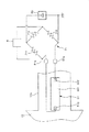
図1は、本発明の第1実施形態に係る光スキャナーを示す平面図、図2は、図1に示す光スキャナーの断面図(X軸に沿った断面図)、図3は、図1に示す光スキャナーの制御系を示すブロック図である。また、図4は、図1に示す光スキャナーが備える駆動部の電圧印加部を説明するためのブロック図、図5は、図4に示す第1の電圧発生部および第2の電圧発生部での発生電圧の一例を示す図である。
なお、以下では、説明の便宜上、図2中の上側を「上」、下側を「下」と言う。
DESCRIPTION OF EXEMPLARY EMBODIMENTS Hereinafter, preferred embodiments of an optical scanner, an image display device, and a head mounted display according to the invention will be described with reference to the accompanying drawings.
(Optical scanner)
<First Embodiment>
FIG. 1 is a plan view showing an optical scanner according to the first embodiment of the present invention, FIG. 2 is a cross-sectional view (cross-sectional view along the X axis) of the optical scanner shown in FIG. 1, and FIG. It is a block diagram which shows the control system of the optical scanner shown. 4 is a block diagram for explaining a voltage application unit of a drive unit included in the optical scanner shown in FIG. 1, and FIG. 5 shows a first voltage generation unit and a second voltage generation unit shown in FIG. It is a figure which shows an example of the generated voltage.
In the following, for convenience of explanation, the upper side in FIG. 2 is referred to as “upper” and the lower side is referred to as “lower”.
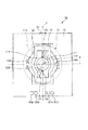
図1および図2に示すように、光スキャナー1は、可動ミラー部11と、1対の軸部12a、12b(第1軸部)と、枠体部13と、1対の軸部14a、14b(第2軸部)と、固定部15と、永久磁石21と、コイル31と、磁心32と、電圧印加部4と、歪検出素子51(第1歪検出素子)および歪検出素子52(第2歪検出素子)とを備える。
ここで、可動ミラー部11、1対の軸部12a、12bは、Y軸(第1の軸)周りに揺動(往復回動)する第1の振動系を構成する。また、可動ミラー部11、1対の軸部12a、12b、枠体部13、1対の軸部14a、14bおよび永久磁石21は、X軸(第2の軸)周りに揺動(往復回動)する第2の振動系を構成する。
As shown in FIGS. 1 and 2, the
Here, the
また、永久磁石21、コイル31および電圧印加部4は、永久磁石21およびコイル31の磁界の相互作用により、前述した第1の振動系および第2の振動系を駆動(すなわち、可動ミラー部11をX軸およびY軸周りに揺動)させる駆動部を構成する。
特に、光スキャナー1では、歪検出素子51が軸部14aの枠体部13側の端部に配置されており、歪検出素子51の検出信号は、軸部14aの曲げ変形に基づく信号を含み、図3に示すように、第1信号処理回路71に入力される。第1信号処理回路71は、軸部14aの曲げ変形に基づく信号を出力する。第1信号処理回路71から出力された信号は、制御部6に入力される。制御部6は、第1信号処理回路71から出力された信号に基づいて、可動ミラー部11のY軸周りの挙動を検出する。このように、歪検出素子51の検出信号に含まれる軸部14aの曲げ変形に基づく信号を用いて、可動ミラー部11のY軸周りの挙動を検出する。
Further, the
In particular, in the
また、歪検出素子52が軸部14bの枠体部13側の端部に配置されており、歪検出素子52の検出信号は、軸部14bの捩れ変形に基づく信号を含み、図3に示すように、第2信号処理回路72に入力される。第2信号処理回路72は、軸部14bの捩れ変形に基づく信号を出力する。第2信号処理回路72から出力された信号は、制御部6に入力される。制御部6は、第2信号処理回路72から出力された信号に基づいて、可動ミラー部11のX軸周りの挙動を検出する。
Further, the
このような光スキャナー1では、歪検出素子51、52が軸部14a、14bの枠体部13側の端部に配置されているため、歪検出素子51、52に対する外部からの固定部15を介した熱の影響を抑制することができる。ここで、軸部14a、14bの枠体部13側の端部とは、軸部14a、14bのそれぞれの中心から枠体部13側の部分のことをいう。
In such an
以下、光スキャナー1の各部を順次詳細に説明する。
可動ミラー部11は、基部(可動部)111と、スペーサー112を介して基部111に固定された光反射板113とを有する。ここで、基部(可動部)111は固定部15に対して揺動(回動)可能な機能を有するものである。
光反射板113の上面(一方の面)には、光反射性を有する光反射部114が設けられている。
Hereinafter, each part of the
The
A
この光反射板113は、軸部12a、12bに対して光反射板113の板厚方向に離間するとともに、板厚方向からみたときに(以下、「平面視」ともいう)軸部12a、12bと重なって設けられている。
そのため、軸部12aと軸部12bとの間の距離を短くしつつ、光反射板113の板面の面積を大きくすることができる。また、軸部12aと軸部12bとの間の距離を短くすることができることから、枠体部13の小型化を図ることができる。さらに、枠体部13の小型化を図ることができることから、軸部14aと軸部14bとの間の距離を短くすることができる。
このようなことから、光反射板113の板面の面積を大きくしても、光スキャナー1の小型化を図ることができる。
The
Therefore, the area of the plate surface of the
For this reason, even if the area of the plate surface of the
また、光反射板113は、平面視にて、軸部12a、12bの全体を覆うように形成されている。言い換えると、軸部12a、12bは、それぞれ、平面視にて、光反射板113の外周に対して内側に位置している。これにより、光反射板113の板面の面積が大きくなり、その結果、光反射部114の面積を大きくすることができる。また、不要な光(例えば、光反射部114に入射できなかった光)が軸部12a、12bで反射して迷光となるのを抑制することができる。
Further, the
また、光反射板113は、平面視にて、枠体部13の全体を覆うように形成されている。言い換えると、枠体部13は、平面視にて、光反射板113の外周に対して内側に位置している。これにより、光反射板113の板面の面積が大きくなり、その結果、光反射部114の面積を大きくすることができる。また、不要な光が枠体部13で反射して迷光となるのを抑制することができる。
The
さらに、光反射板113は、平面視にて、軸部14a、14bの全体を覆うように形成されている。言い換えると、軸部14a、14bは、それぞれ、平面視にて、光反射板113の外周に対して内側に位置している。これにより、光反射板113の板面の面積が大きくなり、その結果、光反射部114の面積を大きくすることができる。また、不要な光が軸部14a、14bで反射して迷光となるのを抑制することができる。
Furthermore, the
本実施形態では、光反射板113は、平面視にて、円形をなしている。なお、光反射板113の平面視形状は、これに限定されず、例えば、楕円形、四角形等の多角形であってもよい。また、光反射板113の平面視形状をX軸およびY軸に沿った方向に突出した形状にすることで、光反射板113の慣性モーメントを小さく抑えつつ各軸部での迷光を効率よく低減できる。
このような光反射板113の下面(他方の面、光反射板113の基部111側の面)には、硬質層115が設けられている。
In the present embodiment, the
A
硬質層115は、光反射板113本体の構成材料よりも硬質な材料で構成されている。これにより、光反射板113の剛性を高めることができる。そのため、光反射板113の揺動時における撓みを抑制することができる。また、光反射板113の厚さを薄くし、光反射板113のX軸およびY軸周りの揺動時における慣性モーメントを抑えることができる。
このような硬質層115の構成材料としては、光反射板113本体の構成材料よりも硬質な材料であれば、特に限定されず、例えば、ダイヤモンド、水晶、サファイヤ、タンタル酸リチウム、ニオブ酸カリウム、カーボンナイトライド膜などを用いることができるが、特に、ダイヤモンドを用いるのが好ましい。
The
The constituent material of such a
硬質層115の厚さ(平均)は、特に限定されないが、1〜10μm程度であるのが好ましく、1〜5μm程度であるのがさらに好ましい。
また、硬質層115は、単層で構成されていてもよいし、複数の層の積層体で構成されていてもよい。また、硬質層115は、光反射板113の下面全体に設けられていてもよいし、下面の一部に設けられていてもよい。なお、硬質層115は、必要に応じて設けられるものであり、省略することもできる。
このような硬質層115の形成には、例えば、プラズマCVD、熱CVD、レーザーCVDのような化学蒸着法(CVD)、真空蒸着、スパッタリング、イオンプレーティング等の乾式メッキ法、電解メッキ、浸漬メッキ、無電解メッキ等の湿式メッキ法、溶射、シート状部材の接合等を用いることができる。
The thickness (average) of the
Moreover, the
The
また、光反射板113の下面は、スペーサー112を介して基部111に固定されている。これにより、軸部12a、12b、枠体部13および軸部14a、14bとの接触を抑制しつつ、光反射板113をY軸周りに揺動させることができる。
また、基部111は、平面視にて、光反射板113の外周に対して内側に位置している。また、基部111の平面視での面積は、基部111がスペーサー112を介して光反射板113を支持することができれば、できるだけ小さいのが好ましい。これにより、光反射板113の板面の面積を大きくしつつ、軸部12aと軸部12bとの間の距離を小さくすることができる。
In addition, the lower surface of the
In addition, the
枠体部13は、枠状をなし、前述した可動ミラー部11の基部111を囲んで設けられている。言い換えると、可動ミラー部11の基部111は、枠状をなす枠体部13の内側に設けられている。
この枠体部13は、平面視にて、可動ミラー部11の基部111および1対の軸部12a、12bからなる構造体の外形に沿った形状をなしている。これにより、可動ミラー部11、1対の軸部12a、12bで構成された第1の振動系の振動、すなわち、可動ミラー部11のY軸周りの揺動を許容しつつ、枠体部13の小型化を図ることができる。
また、枠体部13は、枠体部13の厚さ方向に軸部12a、12bおよび軸部14a、14bよりも突出したリブ131を有する。このようなリブ131により枠体部13の変形を小さくすることができる。また、このリブ131は、可動ミラー部11が永久磁石21に接触するのを抑制する機能(スペーサーとしての機能)も有する。
なお、枠体部13の形状は、枠状であれば、図示のものに限定されない。
The
The
In addition, the
In addition, if the shape of the
また、枠体部13は、Y軸に沿った方向での長さがX軸に沿った方向での長さよりも長くなっている。これにより、軸部12a、12bに必要な長さを確保しつつ、X軸に沿った方向における光スキャナー1の長さを短くすることができる。
そして、枠体部13は、軸部14a、14bを介して固定部15に支持されている。また、可動ミラー部11の基部111は、軸部12a、12bを介して枠体部13に支持されている。
Further, the
And the
軸部12a、12bおよび軸部14a、14bは、それぞれ、弾性変形可能である。
そして、軸部12a、12b(第1軸部)は、可動ミラー部11をY軸(第1の軸)周りに揺動(回動)可能とするように、可動ミラー部11と枠体部13とを接続している。また、軸部14a、14b(第2軸部)は、枠体部13をY軸に直交するX軸(第2の軸)周りに揺動(回動)可能とするように、枠体部13と固定部15とを接続している。
より具体的に説明すると、軸部12a、12bは、可動ミラー部11の基部111を介して(挟んで)互いに対向するように配置されている。
The
The
More specifically, the
また、軸部12a、12bは、それぞれ、Y軸に沿った方向に延びる長手形状(棒状)をなしている。そして、軸部12a、12bは、それぞれ、一方の端部が基部111に接続され、他方の端部が枠体部13に接続されている。また、軸部12a、12bは、それぞれ、中心軸がY軸に一致するように配置されている。
このように、軸部12a、12bは、可動ミラー部11の基部111を両側から支持している。そして、軸部12a、12bは、それぞれ、可動ミラー部11のY軸周りの揺動に伴って捩れ変形する。
なお、軸部12a、12bの形状は、それぞれ、可動ミラー部11を枠体部13に対してY軸周りに揺動可能に支持するものであれば、前述したものに限定されず、例えば、途中の少なくとも1箇所に、屈曲または湾曲した部分、分岐した部分、幅の異なる部分を有していてもよい。
Each of the
Thus, the
The shapes of the
軸部14a、14bは、枠体部13を介して互いに対向するように配置されている。
また、1対の軸部14a、14bは、それぞれ、平面視にてX軸上に沿って配置され、X軸に沿った長手形状(棒状)をなしている。そして、軸部14a、14bは、それぞれ、一方の端部が枠体部13に接続され、他方の端部が固定部15に接続されている。また、軸部14a、14bは、それぞれ、中心軸がX軸に一致するように配置されている。
このように、軸部14a、14bは、枠体部13を両側から支持している。そして、軸部14a、14bは、それぞれ、枠体部13のX軸周りの揺動に伴って捩れ変形する。
The
Further, each of the pair of
Thus, the
なお、軸部14a、14bの形状は、それぞれ、枠体部13を固定部15に対してX軸周りに揺動可能に支持するものであれば、前述したものに限定されず、例えば、途中の少なくとも1箇所に、屈曲または湾曲した部分、分岐した部分、幅の異なる部分を有していてもよい。
このように、可動ミラー部11をY軸周りに揺動可能とするとともに、枠体部13をX軸周りに揺動可能とすることにより、可動ミラー部11(換言すれば光反射板113)を互いに直交するX軸およびY軸の2軸周りに揺動(回動)させることができる。
以上説明したような基部111、軸部12a、12b、枠体部13、軸部14a、14bおよび固定部15は、一体的に形成されている。
Note that the shapes of the
As described above, the movable mirror unit 11 (in other words, the light reflecting plate 113) can be swung around the Y axis and the
The
本実施形態では、基部111、軸部12a、12b、枠体部13、軸部14a、14bおよび固定部15は、第1のSi層(デバイス層)と、SiO2層(ボックス層)と、第2のSi層(ハンドル層)とがこの順に積層したSOI基板をエッチングすることにより形成されている。これにより、第1の振動系および第2の振動系の振動特性を優れたものとすることができる。また、SOI基板は、エッチングにより微細な加工が可能であるため、SOI基板を用いて基部111、軸部12a、12b、枠体部13、軸部14a、14bおよび固定部15を形成することにより、これらの寸法精度を優れたものとすることができ、また、光スキャナー1の小型化を図ることができる。
そして、基部111、軸部12a、12bおよび軸部14a、14bは、それぞれ、SOI基板の第1のSi層で構成されている。これにより、軸部12a、12bおよび軸部14a、14bの弾性を優れたものとすることができる。また、基部111がY軸周りに回動する際に枠体部13に接触するのを抑制することができる。
In the present embodiment, the
The
ここで、このSOI基板の第1のSi層は、p型シリコン単結晶基板またはn型シリコン単結晶基板である。そして、例えば、この第1のSi層が(100)面のp型シリコン単結晶基板である場合、軸部14a、14bは、それぞれ、(100)面のp型シリコン単結晶基板の結晶軸の<110>方向に沿って延びている。また、この第1のSi層が(100)面のn型シリコン単結晶基板である場合、軸部14a、14bは、それぞれ、(100)面のn型シリコン単結晶基板の結晶軸の<100>方向に沿って延びている。
Here, the first Si layer of the SOI substrate is a p-type silicon single crystal substrate or an n-type silicon single crystal substrate. For example, when the first Si layer is a (100) plane p-type silicon single crystal substrate, the
また、枠体部13および固定部15は、それぞれ、SOI基板の第1のSi層、SiO2層および第2のSi層からなる積層体で構成されている。これにより、枠体部13および固定部15の剛性を優れたものとすることができる。
また、枠体部13のSiO2層および第2のSi層、すなわち、枠体部13の軸部12a、12bまたは軸部14a、14bよりも厚さ方向に突出した部分は、前述した枠体部13の剛性を高めるリブ131を構成する。
Further, the
Further, the SiO 2 layer and the second Si layer of the
また、平面視にて、光反射板113の外側に位置する部分(本実施形態では、固定部15)の上面には、反射防止処理が施されているのが好ましい。これにより、光反射板113以外に照射された不要光が迷光となるのを抑制することができる。
かかる反射防止処理としては、特に限定されないが、例えば、反射防止膜(誘電体多層膜)の形成、粗面化処理、黒色処理等が挙げられる。
なお、前述した基部111、軸部12a、12b、枠体部13、軸部14a、14bおよび固定部15の構成材料および形成方法は、一例であり、本発明は、これに限定されるものではない。例えば、シリコン基板をエッチングすることにより、基部111、軸部12a、12b、枠体部13、軸部14a、14bおよび固定部15を形成してもよい。
Moreover, it is preferable that the upper surface of the portion (in the present embodiment, the fixing portion 15) located outside the
The antireflection treatment is not particularly limited, and examples thereof include formation of an antireflection film (dielectric multilayer film), roughening treatment, and black treatment.
In addition, the constituent material and the formation method of the
また、本実施形態では、スペーサー112および光反射板113も、SOI基板をエッチングすることにより形成されている。そして、スペーサー112は、SOI基板のSiO2層および第2のSi層からなる積層体で構成されている。また、光反射板113は、SOI基板の第1のSi層で構成されている。
このように、SOI基板を用いてスペーサー112および光反射板113を形成することにより、互いに接合されたスペーサー112および光反射板113を簡単かつ高精度に製造することができる。
このようなスペーサー112は、例えば、接着剤、ろう材等の接合材(図示せず)により基部111に接合されている。
In this embodiment, the
Thus, by forming the
Such a
固定部15は、枠体部13を支持するものであれば、前述したものに限定されず、例えば、固定部15と軸部14a、14bが別体であってもよい。
前述した枠体部13の下面(光反射板113とは反対側の面)、すなわちリブ131の先端面には、永久磁石21が接合されている。
永久磁石21と枠体部13との接合方法としては、特に限定されないが、例えば、接着剤を用いた接合方法を用いることができる。
永久磁石21は、平面視にて、X軸およびY軸に対して傾斜する方向に磁化されている。
The fixing
The
Although it does not specifically limit as a joining method of the
The
本実施形態では、永久磁石21は、X軸およびY軸に対して傾斜する方向に延在する長手形状(棒状)をなす。そして、永久磁石21は、その長手方向に磁化されている。すなわち、永久磁石21は、一端部をS極とし、他端部をN極とするように磁化されている。
また、永久磁石21は、平面視にて、X軸とY軸との交点を中心として対称となるように設けられている。
In the present embodiment, the
Further, the
なお、本実施形態では、枠体部13に1つの永久磁石の数を設置した場合を例に説明するが、これに限定されず、例えば、枠体部13に2つの永久磁石を設置してもよい。この場合、例えば、長尺状をなす2つの永久磁石を、平面視にて基部111を介して互いに対向するとともに、互いに平行となるように、枠体部13に設置すればよい。
In this embodiment, the case where the number of one permanent magnet is installed in the
X軸に対する永久磁石21の磁化の方向(延在方向)の傾斜角θは、特に限定されないが、30°以上60°以下であるのが好ましく、30°以上45°以下であることがより好ましく、45°であるのがさらに好ましい。このように永久磁石21を設けることで、円滑かつ確実に可動ミラー部11をX軸の周りに回動させることができる。
これに対し、傾斜角θが前記下限値未満であると、電圧印加部4によりコイル31に印加される電圧の強さなどの諸条件によっては、可動ミラー部11を十分にX軸周りに回動させることができない場合がある。一方、傾斜角θが前記上限値を超えると、諸条件によっては、可動ミラー部11を十分にY軸周りに回動させることができない場合がある。
The inclination angle θ in the magnetization direction (extending direction) of the
On the other hand, if the tilt angle θ is less than the lower limit value, the
このような永久磁石21としては、例えば、ネオジム磁石、フェライト磁石、サマリウムコバルト磁石、アルニコ磁石、ボンド磁石等を好適に用いることができる。このような永久磁石21は、高磁性体を着磁したものであり、例えば、着磁前の硬磁性体を枠体部13に設置した後に着磁することにより形成される。既に着磁がなされた永久磁石21を枠体部13に設置しようとすると、外部や他の部品の磁界の影響により、永久磁石21を所望の位置に設置できない場合があるからである。
永久磁石21の直下には、コイル31が設けられている。すなわち、枠体部13の下面に対向するように、コイル31が設けられている。これにより、コイル31から発生する磁界を効率的に永久磁石21に作用させることができる。これにより、光スキャナー1の省電力化および小型化を図ることができる。
As such a
A
本実施形態では、コイル31は、磁心32に巻回されて設けられている。これにより、コイル31で発生した磁界を効率的に永久磁石21に作用させることができる。なお、磁心32は、省略してもよい。
このようなコイル31は、電圧印加部4に電気的に接続されている。
そして、電圧印加部4によりコイル31に電圧が印加されることで、コイル31からX軸およびY軸に直交する方向の磁界が発生する。
In the present embodiment, the
Such a
Then, when a voltage is applied to the
電圧印加部4は、図4に示すように、可動ミラー部11をY軸周りに回動させるための第1の電圧V1を発生させる第1の電圧発生部41と、可動ミラー部11をX軸周りに回動させるための第2の電圧V2を発生させる第2の電圧発生部42と、第1の電圧V1と第2の電圧V2とを重畳する電圧重畳部43とを備え、電圧重畳部43で重畳した電圧をコイル31に印加する。
As shown in FIG. 4, the
第1の電圧発生部41は、図5(a)に示すように、周期T1で周期的に変化する第1の電圧V1(水平走査用電圧)を発生させるものである。すなわち、第1の電圧発生部41は、第1周波数(1/T1)の第1の電圧V1を発生させるものである。
第1の電圧V1は、正弦波のような波形をなしている。そのため、光スキャナー1は効果的に光を主走査することができる。なお、第1の電圧V1の波形は、これに限定されない。
また、第1周波数(1/T1)は、水平走査に適した周波数であれば、特に限定されないが、10〜40kHzであるのが好ましい。
As shown in FIG. 5A, the first voltage generator 41 generates a first voltage V 1 (horizontal scanning voltage) that periodically changes in a cycle T 1 . That is, the first voltage generator 41 generates the first voltage V 1 having the first frequency (1 / T 1 ).
First voltages V 1 is a waveform like a sine wave. Therefore, the
The first frequency (1 / T 1 ) is not particularly limited as long as it is a frequency suitable for horizontal scanning, but is preferably 10 to 40 kHz.
本実施形態では、第1周波数は、可動ミラー部11、1対の軸部12a、12bで構成される第1の振動系(捩り振動系)の捩り共振周波数(f1)と等しくなるように設定されている。つまり、第1の振動系は、その捩り共振周波数f1が水平走査に適した周波数になるように設計(製造)されている。これにより、可動ミラー部11のY軸周りの回動角を大きくすることができる。
In the present embodiment, the first frequency is set to be equal to the torsional resonance frequency (f1) of the first vibration system (torsional vibration system) composed of the
一方、第2の電圧発生部42は、図5(b)に示すように、周期T1と異なる周期T2で周期的に変化する第2の電圧V2(垂直走査用電圧)を発生させるものである。すなわち、第2の電圧発生部42は、第2周波数(1/T2)の第2の電圧V2を発生させるものである。
第2の電圧V2は、鋸波のような波形をなしている。そのため、光スキャナー1は効果的に光を垂直走査(副走査)することができる。なお、第2の電圧V2の波形は、これに限定されない。
On the other hand, as shown in FIG. 5B, the
Second voltage V 2 has a waveform like a sawtooth wave. Therefore, the
第2周波数(1/T2)は、第1周波数(1/T1)と異なり、かつ、垂直走査に適した周波数であれば、特に限定されないが、30〜120Hz(60Hz程度)であるのが好ましい。このように、第2の電圧V2の周波数を60Hz程度とし、前述したように第1の電圧V1の周波数を10〜40kHzとすることで、ディスプレイでの描画に適した周波数で、可動ミラー部11を互いに直交する2軸(X軸およびY軸)のそれぞれの軸周りに回動させることができる。ただし、可動ミラー部11をX軸およびY軸のそれぞれの軸周りに回動させることができれば、第1の電圧V1の周波数と第2の電圧V2の周波数との組み合わせは、特に限定されない。
The second frequency (1 / T 2 ) is different from the first frequency (1 / T 1 ) and is not particularly limited as long as the frequency is suitable for vertical scanning, but is 30 to 120 Hz (about 60 Hz). Is preferred. Thus, the second frequency of the voltage V 2 is set to about 60 Hz, the frequency of the first voltage V 1 as described above by a 10 to 40 kHz, at a frequency suitable for rendering on the display, movable mirrors The
本実施形態では、第2の電圧V2の周波数は、可動ミラー部11、1対の軸部12a、12b、枠体部13、1対の軸部14a、14bおよび永久磁石21で構成された第2の振動系(捩り振動系)の捩り共振周波数(共振周波数)と異なる周波数となるように調整されている。
このような第2の電圧V2の周波数(第2周波数)は、第1の電圧V1の周波数(第1周波数)よりも小さいことが好ましい。すなわち、周期T2は、周期T1よりも長いことが好ましい。これにより、より確実かつより円滑に、可動ミラー部11をY軸周りに第1周波数で回動させつつ、X軸周りに第2周波数で回動させることができる。
In the present embodiment, the frequency of the second voltage V 2 is configured by the
The second voltage V 2 of the frequency (second frequency) is preferably smaller than the first voltage V 1 of the frequency (first frequency). That is, the period T 2 are, is preferably longer than the period T 1. Thereby, the
また、第1の振動系の捩り共振周波数をf1[Hz]とし、第2の振動系の捩り共振周波数をf2[Hz]としたとき、f1とf2とが、f2<f1の関係を満たすことが好ましく、f1≧10f2の関係を満たすことがより好ましい。これにより、より円滑に、可動ミラー部11を、Y軸周りに第1の電圧V1の周波数で回動させつつ、X軸周りに第2の電圧V2の周波数で回動させることができる。これに対し、f1≦f2とした場合は、第2周波数による第1の振動系の振動が起こる可能性がある。
このような第1の電圧発生部41および第2の電圧発生部42は、それぞれ、制御部6に接続され、この制御部6からの信号に基づき駆動する。このような第1の電圧発生部41および第2の電圧発生部42には、電圧重畳部43が接続されている。
電圧重畳部43は、コイル31に電圧を印加するための加算器43aを備えている。加算器43aは、第1の電圧発生部41から第1の電圧V1を受けるとともに、第2の電圧発生部42から第2の電圧V2を受け、これらの電圧を重畳しコイル31に印加するようになっている。
Further, when the torsional resonance frequency of the first vibration system is f1 [Hz] and the torsional resonance frequency of the second vibration system is f2 [Hz], f1 and f2 satisfy the relationship of f2 <f1. Is preferable, and it is more preferable to satisfy the relationship of f1 ≧ 10f2. Thereby, the
The first voltage generation unit 41 and the second
The
次に、光スキャナー1の駆動方法について説明する。なお、本実施形態では、前述したように、第1の電圧V1の周波数は、第1の振動系の捩り共振周波数と等しく設定されており、第2の電圧V2の周波数は、第2の振動系の捩り共振周波数と異なる値に、かつ、第1の電圧V1の周波数よりも小さくなるように設定されている(例えば、第1の電圧V1の周波数が18kHz、第2の電圧V2の周波数が60Hzに設定されている)。
Next, a method for driving the
例えば、図5(a)に示すような第1の電圧V1と、図5(b)に示すような第2の電圧V2とを電圧重畳部43にて重畳し、重畳した電圧をコイル31に印加する。
すると、第1の電圧V1によって、永久磁石21の一方の磁極をコイル31に引き付けようとするとともに、永久磁石21の他方の磁極をコイル31から離間させようとする磁界(この磁界を「磁界A1」という)と、永久磁石21の一方の磁極211をコイル31から離間させようとするとともに、永久磁石21の他方の磁極212をコイル31に引き付けようとする磁界(この磁界を「磁界A2」という)とが交互に切り換わる。
For example, the first voltage V 1 as shown in FIG. 5A and the second voltage V 2 as shown in FIG. 5B are superimposed by the
Then, the first voltage V 1 is used to attract one magnetic pole of the
ここで、上述したように、図1の平面視において、Y軸を挟んで一方側に永久磁石21のN極が位置し、他方側に永久磁石21のS極が位置している。そのため、磁界A1と磁界A2とが交互に切り換わることで、枠体部13にY軸周りの捩り振動成分を有する振動が励振され、その振動に伴って、軸部12a、12bを捩れ変形させつつ、可動ミラー部11が第1の電圧V1の周波数でY軸まわりに回動する。
また、第1の電圧V1の周波数は、第1の振動系の捩り共振周波数と等しい。そのため、第1の電圧V1によって、効率的に、可動ミラー部11をY軸周りに回動させることができる。すなわち、前述した枠体部13のY軸周りの捩り振動成分を有する振動が小さくても、その振動に伴う可動ミラー部11のY軸周りの回動角を大きくすることができる。
Here, as described above, in the plan view of FIG. 1, the north pole of the
Also, the frequency of the first voltage V 1 is equal to the torsional resonance frequency of the first vibration system. Therefore, the
一方、第2の電圧V2によって、永久磁石21の一方の磁極211をコイル31に引き付けようとするとともに、永久磁石21の他方の磁極212をコイル31から離間させようとする磁界(この磁界を「磁界B1」という)と、永久磁石21の一方の磁極211をコイル31から離間させようとするとともに、永久磁石21の他方の磁極212をコイル31に引き付けようとする磁界(この磁界を「磁界B2」という)とが交互に切り換わる。
On the other hand, the second voltage V 2 tries to attract one magnetic pole 211 of the
ここで、上述したように、図1の平面視において、X軸を挟んで一方側に永久磁石21のN極が位置し、他方側に永久磁石21のS極が位置している。そのため、磁界B1と磁界B2とが交互に切り換わることで、軸部14a、14bをそれぞれ捩れ変形させつつ、枠体部13が可動ミラー部11とともに、第2の電圧V2の周波数でX軸周りに回動する。
また、第2の電圧V2の周波数は、第1の電圧V1の周波数に比べて極めて低く設定されている。また、第2の振動系の捩り共振周波数は、第1の振動系の捩り共振周波数よりも低く設計されている。そのため、可動ミラー部11が第2の電圧V2の周波数でY軸周りに回動してしまうことを抑制することができる。
Here, as described above, the N pole of the
Also, the frequency of the second voltage V 2 is set extremely low in comparison with the first frequency of the voltage V 1. Further, the torsional resonance frequency of the second vibration system is designed to be lower than the torsional resonance frequency of the first vibration system. Therefore, it is possible to prevent the
このように、第1の電圧V1と第2の電圧V2とを重畳させた電圧をコイル31に印加することで、可動ミラー部11を、Y軸周りに第1の電圧V1の周波数で回動させつつ、X軸周りに第2の電圧V2の周波数で回動させることができる。これにより、装置の低コスト化および小型化を図るとともに、電磁駆動方式(ムービングマグネット方式)により、可動ミラー部11をX軸およびY軸のそれぞれの軸周りに回動させることができる。また、駆動源を構成する部品(永久磁石およびコイル)の数を少なくすることができるため、簡単かつ小型な構成とすることができる。また、コイル31が光スキャナー1の振動系と離間しているので、かかる振動系に対するコイル31の発熱による悪影響を抑制することができる。
このような可動ミラー部11の挙動は、歪検出素子51、52の検出信号に基づいて検出される。
In this way, by applying a voltage obtained by superimposing the first voltage V 1 and the second voltage V 2 to the
Such behavior of the
以下、歪検出素子51、52について詳述する。
図6は、図1に示す光スキャナーの第1歪検出素子を説明するための図、図7は、図1に示す光スキャナーの第2歪検出素子を説明するための図である。
歪検出素子51(第1歪検出素子)は、軸部14aの枠体部13側の端部に配置され、軸部14aの変形(主に曲げ変形)を検出する。これにより、可動ミラー部11に入射した光による熱が歪検出素子51に与える影響を抑制することができる。また、可動ミラー部11のY軸周りの挙動の検出に用いる歪抵抗素子を軸部12a、12bに設ける必要がないため、軸部12a、12bの設計の自由度を高めることができる。
Hereinafter, the
6 is a diagram for explaining the first strain detection element of the optical scanner shown in FIG. 1, and FIG. 7 is a diagram for explaining the second strain detection element of the optical scanner shown in FIG.
The strain detection element 51 (first strain detection element) is disposed at the end of the
この歪検出素子51は、2端子型のピエゾ抵抗素子である。
具体的に説明すると、歪検出素子51は、図6に示すように、ピエゾ抵抗領域511と、ピエゾ抵抗領域511上に配置された1対の端子512、513とを有している。
ピエゾ抵抗領域511は、軸部14a表面に不純物をドーピングすることにより形成されている。より具体的には、軸部14aがp型シリコン単結晶基板を加工することにより形成されている場合、ピエゾ抵抗領域511は、軸部14a表面にリン等の不純物をドーピングすることにより形成されたn型シリコン単結晶(n型抵抗領域)である。一方、軸部14aがn型シリコン単結晶基板を加工することにより形成されている場合、ピエゾ抵抗領域511は、軸部14a表面にボロン等の不純物をドーピングすることにより形成されたp型シリコン単結晶(p型抵抗領域)である。
The
More specifically, as shown in FIG. 6, the
The
また、ピエゾ抵抗領域511は、軸部14aの長手方向(すなわちX軸方向)に沿った方向に延びる長手形状をなしている。また、ピエゾ抵抗領域511は、平面視にて、軸部14aの幅方向での中央部に配置されている。
なお、本実施形態では、ピエゾ抵抗領域511全体が軸部14a上に設けられているが、ピエゾ抵抗領域511は、軸部14aの曲げ変形による引張応力または圧縮応力を受けることができれば、図示の位置に限定されず、例えば、軸部14aと固定部15との境界部を跨るように設けられていてもよい。
このようなピエゾ抵抗領域511上には、軸部14aの長手方向(すなわちX軸方向)に沿った方向に並んで1対の端子512、513が配置されている。
The
In the present embodiment, the entire
On such a
本実施形態では、ピエゾ抵抗領域511の長手方向での両端部に1対の端子512、513が配置されている。
1対の端子512、513は、第1信号処理回路71に電気的に接続されている。
このような歪検出素子51では、軸部14aの曲げ変形に伴ってピエゾ抵抗領域511に引張応力または圧縮応力が生じると、その引張応力または圧縮応力の程度に応じて、ピエゾ抵抗領域511の比抵抗値が変化する。
本実施形態では、ピエゾ抵抗領域511がX軸方向に延びる長手形状をなすとともに1対の端子512、513がピエゾ抵抗領域511上にX軸方向に並んで配置されているので、歪検出素子51から出力される信号に含まれる軸部14aの曲げ変形に基づく信号を大きくすることができる。
In the present embodiment, a pair of
The pair of
In such a
In the present embodiment, the
ここで、ピエゾ抵抗領域511および1対の端子512、513が平面視にてX軸に対して対称となるように配置されている。そのため、歪検出素子51は、軸部14aの曲げ変形に伴う引張応力または圧縮応力のみを検出することができる。すなわち、歪検出素子51は、軸部14aの捩れ変形に伴うせん断が検出されないようにすることができる。そのため、歪検出素子51から出力される信号に、軸部14aの捩れ変形に基づく信号が含まれるのを抑制または防止することができる。その結果、歪検出素子51から出力される信号を用いて、比較的簡単な構成で、可動ミラー部11のY軸周りの挙動を高精度に検出することができる。
このような歪検出素子51の検出信号は、固定部15に設けられた1対の端子81a、81bを介して、第1信号処理回路71(第1信号処理部)に入力される。
Here, the
Such a detection signal of the
第1信号処理回路71は、歪検出素子51の検出信号を所定の処理により信号処理に適した信号に変換する機能を有する。
第1信号処理回路71における具体的な処理としては、例えば、インピーダンス変換、温度補償、信号増幅、フィルター、ADコンバーター等が挙げられる。
前述したように、歪検出素子51の検出信号は、軸部14aの曲げ変形に基づく信号を含んでいる。そして、第1信号処理回路71は、上述したような処理を必要に応じて行って、軸部14aの曲げ変形に基づく信号を出力する。これにより、第1信号処理回路71から出力された信号に基づいて、可動ミラー部11のY軸周りの挙動を検出することができる。
The first
Specific processing in the first
As described above, the detection signal of the
本実施形態では、第1信号処理回路71は、図6に示すように、抵抗素子711、712、713を有している。
この抵抗素子711、712、713および歪検出素子51は、ブリッジ回路(ホイートストンブリッジ回路)を構成している。このブリッジ回路は、歪検出素子駆動回路53により電力が供給され、歪検出素子51の抵抗値の変化に応じた信号(電圧)を制御部6へ出力する。
このような抵抗素子711、712、713は、それぞれ、歪検出素子51と同等の温度特性を有していることが好ましい。これにより、歪検出素子51の温度特性によらず、軸部14aの曲げ変形量に応じた信号(電圧)を安定して出力することができる。
In the present embodiment, the first
The
Each of
なお、抵抗素子711、712、713は、軸部14a、14bの変形に伴う応力を受けない位置で、固定部15に配置してもよい。この場合、抵抗素子711、712、713は、それぞれ、歪検出素子51のピエゾ抵抗領域と同様に構成された抵抗領域と、その抵抗領域に設けられた1対の端子とで構成することができる。また、この場合、抵抗素子711、712、713は、それぞれ、歪検出素子51と同等の温度条件となる位置に配置されることが好ましい。
このような第1信号処理回路71から出力された信号は、図3に示す制御部6に入力される。
Note that the
Such a signal output from the first
一方、歪検出素子52は、軸部14bの枠体部13側の端部に配置され、軸部14bの変形(主に捩れ変形)を検出する。これにより、可動ミラー部11に入射した光による熱が歪検出素子52に与える影響を抑制することができる。また、可動ミラー部11のX軸周りの挙動の検出に用いる歪抵抗素子を軸部12a、12bに設ける必要がないため、軸部12a、12bの設計の自由度を高めることができる。
この歪検出素子52は、4端子型のピエゾ抵抗素子である。
具体的に説明すると、歪検出素子52は、図7に示すように、ピエゾ抵抗領域521と、ピエゾ抵抗領域521上に配置された1対の入力端子522、523および1対の出力端子524、525とを有している。
On the other hand, the
The
More specifically, as shown in FIG. 7, the
ピエゾ抵抗領域521は、軸部14b表面に不純物をドーピングすることにより形成されている。より具体的には、軸部14bがp型シリコン単結晶基板を加工することにより形成されている場合、ピエゾ抵抗領域521は、軸部14b表面にリン等の不純物をドーピングすることにより形成されたn型シリコン単結晶(n型抵抗領域)である。一方、軸部14bがn型シリコン単結晶基板を加工することにより形成されている場合、ピエゾ抵抗領域521は、軸部14b表面にボロン等の不純物をドーピングすることにより形成されたp型シリコン単結晶(p型抵抗領域)である。
The
本実施形態では、ピエゾ抵抗領域521は、平面視にて、X軸方向に沿った1対の辺と、Y軸方向に沿った1対の辺とを有する四角形をなしている。
なお、本実施形態では、ピエゾ抵抗領域521全体が軸部14b上に設けられているが、ピエゾ抵抗領域521は、軸部14bの捩れ変形によるせん断応力を受けることができれば、図示の位置に限定されず、例えば、軸部14bと固定部15との境界部を跨るように設けられていてもよい。
このようなピエゾ抵抗領域521上には、軸部14bの長手方向(すなわちX軸方向)に沿った方向に並んで1対の入力端子522、523が配置されているとともに、軸部14bの長手方向に対して垂直な方向(すなわちY軸方向)に沿った方向に並んで1対の出力端子524、525が配置されている。
In the present embodiment, the
In the present embodiment, the entire
On such a
本実施形態では、ピエゾ抵抗領域521のX軸方向での両端部に1対の入力端子522、523が配置され、ピエゾ抵抗領域521のY軸方向での両端部に1対の出力端子524、525が配置されている。
1対の入力端子522、523は、固定部15に設けられた1対の端子82a、82bを介して、歪検出素子駆動回路53に電気的に接続されている。
In the present embodiment, a pair of
The pair of
一方、1対の出力端子524、525は、固定部15に設けられた1対の端子82c、82dを介して、第2信号処理回路72に電気的に接続されている。
このような歪検出素子52では、歪検出素子駆動回路53が1対の入力端子522、523間に定電圧または定電流で電圧を印加する。これにより、ピエゾ抵抗領域521上に電界Eを生じさせる。この電界Eのもと、軸部14bの捩れ変形に伴ってピエゾ抵抗領域521にせん断応力が生じると、そのせん断応力の程度に応じて、ピエゾ抵抗領域521の比抵抗値が変化し、1対の出力端子524、525間の電位差が変化する。この電位差は、軸部14bの捩れ変形量や、可動ミラー部11および枠体部13のX軸周りの揺動角に応じて変化する。したがって、かかる電位差に基づいて、可動ミラー部11のX軸周りの挙動を検知することができる。
On the other hand, the pair of
In such a
また、このような歪検出素子52は、軸部14bの捩れ変形に伴うせん断応力のみを検出することができる。すなわち、歪検出素子52は、軸部14bの曲げ変形に伴う引張または圧縮応力が検出されないようにすることができる。そのため、歪検出素子52から出力される信号に、軸部14bの曲げ変形に基づく信号が含まれるのを抑制または防止することができる。その結果、歪検出素子52から出力される信号を用いて、比較的簡単な構成で、可動ミラー部11のX軸周りの挙動を高精度に検出することができる。
このような歪検出素子52の検出信号は、第2信号処理回路72(第2信号処理部)に入力される。
Moreover, such a
Such a detection signal of the
第2信号処理回路72は、歪検出素子52の検出信号を所定の処理により信号処理に適した信号に変換する機能を有する。
第2信号処理回路72における具体的な処理としては、例えば、インピーダンス変換、温度補償、信号増幅、フィルター、ADコンバーター等が挙げられる。
前述したように、歪検出素子52の検出信号は、軸部14bの捩れ変形に基づく信号を含んでいる。そして、第2信号処理回路72は、上述したような処理を必要に応じて行って、軸部14bの捩れ変形に基づく信号を出力する。これにより、第2信号処理回路72から出力された信号に基づいて、可動ミラー部11のX軸周りの挙動を検出することができる。
The second
Specific processing in the second
As described above, the detection signal of the
このような第2信号処理回路72から出力された信号は、図3に示す制御部6に入力される。
制御部6では、第1信号処理回路71から出力された信号に基づいて、可動ミラー部11のY軸周りの挙動を検出する。これにより、検出した挙動に基づいて、可動ミラー部11のY軸周りの挙動を所望の状態となるように制御したり、可動ミラー部11のY軸周りの挙動と他の装置の動作とを同期させたりすることができる。
制御部6では、第2信号処理回路72から出力された信号に基づいて、可動ミラー部11のX軸周りの挙動を検出する。これにより、検出した挙動に基づいて、可動ミラー部11のX軸周りの挙動を所望の状態となるように制御したり、可動ミラー部11のX軸周りの挙動と他の装置の動作とを同期させたりすることができる。
The signal output from the second
The
The
本実施形態では、制御部6は、図3に示すように、H検出部61と、V検出部62と、H制御部63と、V制御部64と、H目標値記憶部65と、V目標値生成部66とを有している。
H検出部61は、第1信号処理回路71から出力された信号に基づいて、水平走査の制御に必要な信号として、例えば可動ミラー部11のY軸周りの揺動角に応じた信号を生成する。なお、可動ミラー部11のY軸周りの揺動角の検出方法については、後に詳述する。
V検出部62は、第2信号処理回路72から出力された信号に基づいて、垂直走査の制御に必要な信号として、例えば可動ミラー部11のX軸周りの揺動角に応じた信号を生成する。
In the present embodiment, as shown in FIG. 3, the
Based on the signal output from the first
Based on the signal output from the second
H制御部63は、H目標値記憶部65に予め記憶されたH目標値と、H検出部61から出力された信号とに基づいて、水平走査用の駆動信号を生成する。
H目標値記憶部65には、H目標値として、例えば、水平走査用の駆動信号との位相差、可動ミラー部11のY軸周りの最大揺動角が格納(記憶)されている。
V制御部64は、V目標値生成部66から出力されたV目標値と、V検出部62から出力された信号とに基づいて、垂直走査用の駆動信号を生成する。
V目標値生成部66は、外部から入力された垂直走査方向へのライン情報に基づいて、V目標値として、例えば、可動ミラー部11のX軸周りの揺動角を生成する。
The
The H target
The
The V target
ここで、歪検出素子51の検出信号を用いて可動ミラー部11のY軸周りの挙動を検出する方法について、可動ミラー部11のY軸周りの揺動角を検出する場合を例として説明する。
(第1検出方法)
第1検出方法では、オブザーバーを用いて、第1信号処理回路71から出力された信号に基づいて、可動ミラー部11のY軸周りの挙動(本例では揺動角)を推定する。
Here, a method for detecting the behavior of the
(First detection method)
In the first detection method, the behavior around the Y axis of the movable mirror unit 11 (in this example, the swing angle) is estimated based on the signal output from the first
以下、第1検出方法について詳述する。
光スキャナー1は、前述したように、水平走査のための第1の電圧と垂直走査のための第2の電圧を重畳してコイル31に印加することによって、可動ミラー部11をY軸(第1の軸)周りに第1の電圧の周波数で揺動させるとともにX軸(第2の軸)周りに第2の電圧の周波数で揺動させる。
Hereinafter, the first detection method will be described in detail.
As described above, the
ここで、第1の電圧の周波数(水平走査の駆動周波数)と第2の電圧の周波数(垂直走査の駆動周波数)とは十分に離れているため、第1の電圧によって生じるトルクと第2の電圧によって生じるトルクとのクロストークを考慮しなくてもよい。したがって、光スキャナー1におけるX軸周りに関する運動とY軸周りに関する運動とを独立して考えることができる。
そうすると、光スキャナー1のY軸周りに関する運動方程式は、下記式(1)で表すことができる。
Here, since the frequency of the first voltage (horizontal scanning drive frequency) and the frequency of the second voltage (vertical scanning driving frequency) are sufficiently separated, the torque generated by the first voltage and the second voltage It is not necessary to consider the crosstalk with the torque generated by the voltage. Therefore, the movement about the X axis and the movement about the Y axis in the
Then, the equation of motion about the Y axis of the

ここで、前記式(1)中、θhh:可動ミラー部11のY軸周りの揺動角、θvh:枠体部13のY軸周りの揺動角、Ihh:可動ミラー部11のY軸周りのイナーシャ、Ivh:枠体部13のY軸周りのイナーシャ、Chh:可動ミラー部11のY軸周りの揺動(振動)の減衰係数、Cvh:枠体部13のY軸周りの揺動(振動)の減衰係数、khh:軸部12a、12bのY軸周りの捩りばね定数、kvh:軸部14a、14bのY軸周りの捩りばね定数、T(t):永久磁石21およびコイル31の磁界の相互作用によって枠体部13が受けるY軸周りのトルクである。
Here, in the formula (1), θ hh : the swing angle around the Y axis of the
そして、 And
とし、軸部14aの曲げ応力に関する歪検出素子51の検出信号の出力をyとし、歪検出素子51の変換係数をαとしたとき、前記式(1)から、次に示すようなXおよびyの関係を導くことができる。
When the output of the detection signal of the
このようなXおよびyの関係で与えられるシステムの可観測係数を The observable coefficient of the system given by the relationship between X and y is
とすると、次の式が得られる。 Then, the following equation is obtained.
ここで、Mobs=4であるから、このシステムは可観測である。したがって、軸部14aに配置した歪検出素子51の検出信号に含まれる軸部14aの曲げ変形に基づく信号に基づいて、オブザーバーによって、可動ミラー部11のY軸周りの揺動角(振れ角)を推定することができる。
かかるオブザーバーは、オブザーバーゲインをLとし、Xおよびyの推定値の関係は、次のように表される。
Here, since M obs = 4, this system is observable. Therefore, based on a signal based on the bending deformation of the
In such an observer, the observer gain is L, and the relationship between the estimated values of X and y is expressed as follows.
このようなXおよびyの推定値の関係を用いることにより、歪検出素子51の検出信号に含まれる軸部14aの曲げ変形に基づく信号に基づいて、可動ミラー部11のY軸周りの揺動角を推定することができる。
以上説明したような第1検出方法によれば、可動ミラー部11のY軸周りの揺動が共振状態でなくても、第1信号処理回路71から出力された信号に基づいて、可動ミラー部11のY軸周りの挙動を検出することができる。
By using such a relationship between the estimated values of X and y, based on the signal based on the bending deformation of the
According to the first detection method as described above, based on the signal output from the first
(第2検出方法)
第2検出方法では、可動ミラー部11のY軸周りの揺動に関する共振周波数における振幅と、枠体部13のY軸周りの揺動に関する共振周波数における振幅との比を用いて、第1信号処理回路71から出力された信号に基づいて、可動ミラー部11のY軸周りの挙動(本例では揺動角)を推定する。
(Second detection method)
In the second detection method, the first signal is obtained by using the ratio of the amplitude at the resonance frequency related to the oscillation of the
以下、第2検出方法について詳述する。
前記式(1)において、θhhおよびθvhのラプラス変換をそれぞれXhhおよびXvhとし、初期値をすべて0とすると、下記式(2)が得られる。
Hereinafter, the second detection method will be described in detail.
In the above formula (1), when Laplace transforms of θ hh and θ vh are respectively X hh and X vh and the initial values are all 0, the following formula (2) is obtained.
この式(2)を変形すると、下記式(3)が得られる。 When this equation (2) is transformed, the following equation (3) is obtained.
![]()
![]()
ここで、可動ミラー部11および枠体部13のY軸周りの揺動に関する共振周波数は、それぞれ、前記式(3)の分母が最小となるときのs(=jω、ω:角周波数)によって決まる。前記式(3)からわかるように、XhhおよびXvhの分母は互いに等しいため、可動ミラー部11のY軸周りの揺動に関する共振周波数と、枠体部13のY軸周りの揺動に関する共振周波数とは一致する。
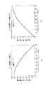
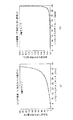
具体的には、枠体部13に印加されるY軸周りのトルクと可動ミラー部11および枠体部13のY軸周りの揺動角との比に関する周波数特性は、図8(a)および図9(a)に示すようになる。
Here, the resonance frequencies related to the swing of the
Specifically, the frequency characteristic regarding the ratio between the torque around the Y axis applied to the
また、枠体部13に印加されるY軸周りのトルクと可動ミラー部11および枠体部13のY軸周りの揺動との位相差に関する周波数特性は、図8(b)および図9(b)に示すようになる。
なお、図8(a)は、枠体部に印加される第1の軸周りのトルクと可動部および枠体部のY軸周りの揺動角との比に関する周波数特性を示すグラフ、図8(b)は、枠体部に印加される第1の軸周りのトルクと可動部および枠体部の第1の軸周りの揺動との位相差に関する周波数特性を示すグラフである。また、図9(a)は、図8(a)の共振周波数付近を拡大したグラフ、図9(b)は、図8(b)の共振周波数付近を拡大したグラフである。
Further, the frequency characteristics regarding the phase difference between the torque around the Y axis applied to the
FIG. 8A is a graph showing frequency characteristics relating to the ratio between the torque around the first axis applied to the frame body part and the swing angle around the Y axis of the movable part and the frame body part. (B) is a graph showing the frequency characteristics regarding the phase difference between the torque around the first axis applied to the frame body and the swing of the movable part and the frame around the first axis. FIG. 9A is a graph in which the vicinity of the resonance frequency in FIG. 8A is enlarged, and FIG. 9B is a graph in which the vicinity of the resonance frequency in FIG. 8B is enlarged.
ところで、可動ミラー部11および枠体部13のY軸周りの揺動は、軸部14a、14bの引張応力として現れる。したがって、軸部14aに配置された歪検出素子51の検出信号に基づいて、可動ミラー部11がY軸周りの揺動に関する共振状態であるか否かを把握することができる。より具体的には、枠体部13に印加されるY軸周りのトルクと可動ミラー部11および枠体部13のY軸周りの揺動との位相差に基づいて、可動ミラー部11がY軸周りの揺動に関する共振状態であるか否かを把握することができる。
By the way, the swing of the
歪検出素子51の検出信号に基づいて可動ミラー部11の揺動角(振れ角)を推定するには、歪検出素子51の応答に、可動ミラー部11のY軸周りの揺動に関する共振状態における可動ミラー部11のY軸周りの振幅と枠体部13のY軸周りの振幅との比を乗じればよい。
かかる比が温度変化により変化する場合には、光スキャナー1付近に温度センサーを設置し、その温度センサーによって検知された温度に応じて、当該比を補正すればよい。
以上説明したような第2検出方法によれば、比較的簡単な構成で、第1信号処理回路71から出力された信号に基づいて、可動ミラー部11のY軸周りの挙動を高精度に検出することができる。
In order to estimate the swing angle (swing angle) of the
When such a ratio changes due to a temperature change, a temperature sensor may be installed near the
According to the second detection method as described above, the behavior around the Y axis of the
以上説明したような光スキャナー1によれば、第1信号処理回路71から出力された信号に基づいて、可動ミラー部11のY軸周りの挙動を検出することができる。また、第2信号処理回路72から出力された信号に基づいて、可動ミラー部11のX軸周りの挙動を検出することができる。また、歪検出素子51、52が軸部14a、14bの枠体部13側の端部に配置されているため、歪検出素子51、52に対する外部からの固定部15を介した熱の影響を抑制することができる。
According to the
<第2実施形態>
次に、本発明の第2実施形態について説明する。
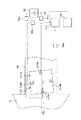
図10は、本発明の第2実施形態に係る光スキャナーを示す平面図、図11は、図10に示す光スキャナーの制御系を示すブロック図である。また、図12は、図10に示す光スキャナーの歪検出素子を説明するための図である。また、図13は、2端子型の歪検出素子の姿勢とシリコンの結晶方位との関係を説明するための図である。また、図14は、ピエゾ抵抗領域にp型シリコンを用いた場合における2端子型の歪検出素子の姿勢(角度α)と引張応力およびせん断応力による抵抗値変化率の絶対値との関係を示すグラフである。また、図15は、ピエゾ抵抗領域にn型シリコンを用いた場合における2端子型の歪検出素子の姿勢(角度α)と引張応力およびせん断応力による抵抗値変化率の絶対値との関係を示すグラフである。また、図16は、2端子型の歪検出素子の姿勢(角度α)と引張応力およびせん断応力による抵抗値変化率の絶対値の比との関係を示すグラフである。
Second Embodiment
Next, a second embodiment of the present invention will be described.
FIG. 10 is a plan view showing an optical scanner according to the second embodiment of the present invention, and FIG. 11 is a block diagram showing a control system of the optical scanner shown in FIG. FIG. 12 is a diagram for explaining a strain detection element of the optical scanner shown in FIG. FIG. 13 is a diagram for explaining the relationship between the orientation of the two-terminal strain detection element and the crystal orientation of silicon. FIG. 14 shows the relationship between the orientation (angle α) of the two-terminal strain detection element and the absolute value of the rate of change in resistance value due to tensile stress and shear stress when p-type silicon is used for the piezoresistive region. It is a graph. FIG. 15 shows the relationship between the attitude (angle α) of the two-terminal strain detection element and the absolute value of the resistance value change rate due to tensile stress and shear stress when n-type silicon is used in the piezoresistive region. It is a graph. FIG. 16 is a graph showing the relationship between the orientation (angle α) of the two-terminal strain detection element and the ratio of the absolute value of the rate of change in resistance value due to tensile stress and shear stress.
本実施形態に係る光スキャナーは、歪検出素子、第1信号処理部および第2信号処理部の構成が異なる以外は、前述した第1実施形態にかかる光スキャナーと同様である。
なお、以下の説明では、第2実施形態に関し、前述した実施形態との相違点を中心に説明し、同様の事項に関してはその説明を省略する。また、図10〜図12において、前述した実施形態と同様の構成については、同一符号を付している。
The optical scanner according to the present embodiment is the same as the optical scanner according to the first embodiment described above except that the configurations of the strain detection element, the first signal processing unit, and the second signal processing unit are different.
In the following description, the second embodiment will be described with a focus on differences from the above-described embodiment, and description of similar matters will be omitted. 10 to 12, the same reference numerals are given to the same configurations as those in the above-described embodiment.
図10に示す光スキャナー1Aは、前述した第1実施形態の歪検出素子51、52に代えて、歪検出素子51A、52Aを有する。また、光スキャナー1Aは、図11に示すように、前述した第1実施形態の第1信号処理回路71および第2信号処理回路72に代えて、第1信号処理回路71Aおよび第2信号処理回路72Aを有する。
歪検出素子51A(第1歪検出素子)は、軸部14aの枠体部13側の端部に配置され、軸部14aの変形(曲げ変形および捩れ変形)を検出する。一方、歪検出素子52A(第2歪検出素子)は、軸部14bの枠体部13側の端部に配置され、軸部14bの変形(曲げ変形および捩れ変形)を検出する。
An optical scanner 1A shown in FIG. 10 includes
The
歪検出素子51A、52Aは、平面視にて、Y軸に対して対称となるように配置されている。なお、以下では、歪検出素子51Aについて主に説明し、歪検出素子52Aについては、歪検出素子51Aと同様であるため、その説明を省略する。
この歪検出素子51Aは、2端子型のピエゾ抵抗素子である。
具体的に説明すると、歪検出素子51Aは、図12に示すように、ピエゾ抵抗領域511Aと、ピエゾ抵抗領域511A上に配置された1対の端子512A、513Aとを有している。
The
The
More specifically, as shown in FIG. 12, the
ピエゾ抵抗領域511Aは、軸部14a表面に不純物をドーピングすることにより形成されている。
また、ピエゾ抵抗領域511Aは、軸部14aの長手方向(すなわちX軸方向)に対して傾斜した方向に延びる長手形状をなしている。また、ピエゾ抵抗領域511Aは、平面視にて、軸部14aの幅方向での中心を跨って配置されている。
The
The
なお、本実施形態では、ピエゾ抵抗領域511A全体が軸部14a上に設けられているが、ピエゾ抵抗領域511Aは、軸部14aの曲げ変形による引張応力または圧縮応力を受けるとともに軸部14aの捩れ変形によるせん断応力を受けることができれば、図示の位置に限定されず、例えば、軸部14aと固定部15との境界部を跨るように設けられていてもよい。
このようなピエゾ抵抗領域511A上には、軸部14aの長手方向(すなわちX軸方向)に対して傾斜した方向に並んで1対の端子512A、513Aが配置されている。
In this embodiment, the entire
On the
本実施形態では、ピエゾ抵抗領域511Aの長手方向での両端部に1対の端子512A、513Aが配置されている。
1対の端子512A、513Aは、第1信号処理回路71Aに電気的に接続されている。なお、図12では、図示しないが、1対の端子512A、513Aは、図11に示す第2信号処理回路72Aにも電気的に接続されている。
このような歪検出素子51Aでは、軸部14aの曲げ変形に伴ってピエゾ抵抗領域511Aに引張応力または圧縮応力が生じると、その引張応力または圧縮応力の程度に応じて、ピエゾ抵抗領域511Aの比抵抗値が変化する。
In the present embodiment, a pair of
The pair of
In such a
また、歪検出素子51Aでは、軸部14aの捩れ変形に伴ってピエゾ抵抗領域511Aにせん断応力が生じると、そのせん断応力の程度に応じて、ピエゾ抵抗領域511Aの比抵抗値が変化する。
したがって、歪検出素子51Aの検出信号は、軸部14aの曲げ変形および捩れ変形に基づく信号を含んでいる。
In the
Therefore, the detection signal of the
本実施形態では、1対の端子512A、513Aがピエゾ抵抗領域511A上にX軸方向に対して傾斜した方向に並んで配置されているので、歪検出素子51Aから出力される信号に含まれる軸部14aの曲げ変形および捩れ変形のそれぞれに基づく信号を大きくすることができる。
このような歪検出素子51Aの検出信号に含まれる軸部14aの曲げ変形に基づく信号と軸部14aの捩れ変形に基づく信号との比は、歪検出素子51Aの角度α(傾斜角度)に応じて変化する。ここで、角度αは、軸部14aの長手方向(すなわちX軸方向)と、1対の端子512A、513Aとが並ぶ方向(1対の端子512、513を最短距離で結ぶ直線の方向)とのなす角度である。
In this embodiment, since the pair of
The ratio of the signal based on the bending deformation of the
以下、歪検出素子51Aの検出信号について、図13に示すように、軸部14aの長手方向をシリコン単結晶の結晶軸の<110>方向とした場合を例に詳細に説明する。
ピエゾ抵抗領域511Aをp型のシリコン単結晶で構成した場合、図14(a)に示すように、1対の端子512A、513A間におけるピエゾ抵抗領域511Aの引張応力に関する抵抗値変化率の絶対値は、角度α(<110>からのオフセット)が大きくなるに従い小さくなる。すなわち、角度αが大きくなるほど、歪検出素子51Aの検出信号に含まれる軸部14aの曲げ変形に基づく信号が小さくなる。
Hereinafter, the detection signal of the
When the
一方、この場合、図14(b)に示すように、1対の端子512A、513A間におけるピエゾ抵抗領域511Aのせん断応力に関する抵抗値変化率の絶対値は、角度αが大きくなるに従い大きくなる。すなわち、角度αが大きくなるほど、歪検出素子51Aの検出信号に含まれる軸部14aの捩れ変形に基づく信号が大きくなる。ただし、捩れ変形に基づく信号の角度αによる変化は、曲げ変形に基づく信号の角度αによる変化よりも小さい。
On the other hand, in this case, as shown in FIG. 14B, the absolute value of the resistance value change rate related to the shear stress of the
また、ピエゾ抵抗領域511Aをn型のシリコン単結晶で構成した場合、図15(a)に示すように、1対の端子512A、513A間におけるピエゾ抵抗領域511Aの引張応力に関する抵抗値変化率の絶対値は、角度αが大きくなるに従い小さくなる。すなわち、角度αが大きくなるほど、歪検出素子51Aの検出信号に含まれる軸部14aの曲げ変形に基づく信号が小さくなる。ただし、曲げ変形に基づく信号の角度αによる変化は小さい。
Further, when the
一方、この場合、図15(b)に示すように、1対の端子512A、513A間におけるピエゾ抵抗領域511Aのせん断応力に関する抵抗値変化率の絶対値は、角度αが大きくなるに従い大きくなる。すなわち、角度αが大きくなるほど、歪検出素子51Aの検出信号に含まれる軸部14aの捩れ変形に基づく信号が大きくなる。しかも、捩れ変形に基づく信号の角度αによる変化は、曲げ変形に基づく信号の角度αによる変化よりも大きい。
On the other hand, in this case, as shown in FIG. 15B, the absolute value of the resistance value change rate related to the shear stress of the
また、ピエゾ抵抗領域511Aをp型のシリコン単結晶で構成した場合、図16(a)に示すように、1対の端子512A、513A間におけるピエゾ抵抗領域511Aの引張応力に関する抵抗値変化率の絶対値(R1)とせん断応力に関する抵抗値変化率の絶対値(R2)との比(R1/R2)は、角度αが大きくなるに従い小さくなる。すなわち、角度αが大きくなるほど、歪検出素子51Aの検出信号に含まれる軸部14aの捩れ変形に基づく信号に対する曲げ変形に基づく信号の割合が小さくなる。
Further, when the
また、ピエゾ抵抗領域511Aをn型のシリコン単結晶で構成した場合も、図16(b)に示すように、1対の端子512A、513A間におけるピエゾ抵抗領域511Aの引張応力に関する抵抗値変化率の絶対値(R1)とせん断応力に関する抵抗値変化率の絶対値(R2)との比(R1/R2)は、角度αが大きくなるに従い小さくなる。すなわち、角度αが大きくなるほど、歪検出素子51Aの検出信号に含まれる軸部14aの捩れ変形に基づく信号に対する曲げ変形に基づく信号の割合が小さくなる。ただし、かかる割合は、角度αによらず小さく、角度αによる変化も小さい。
以上のようなことから、軸部14aの長手方向をシリコン単結晶の結晶軸の<110>方向とした場合、ピエゾ抵抗領域511Aをp型のシリコン単結晶で構成することにより、歪検出素子51Aから出力される信号に含まれる軸部14aの曲げ変形および捩れ変形のそれぞれに基づく信号を効率的に大きくすることができる。
Further, even when the
As described above, when the longitudinal direction of the
また、角度αは、軸部14a、14bを構成するシリコン単結晶の導電型や結晶軸の方向によって異なり、特に限定されないが、例えば、軸部14a、14bの長手方向をシリコン単結晶の結晶軸の<110>方向とし、かつ、ピエゾ抵抗領域511Aをp型のシリコン単結晶で構成した場合、3°以上25°以下であることが好ましく、5°以上8°以下であることがより好ましい。図16(a)に示すように、角度αを3°以上25°以下とすることにより、上述した比(R1/R2)を約10%から90%までの範囲とすることができる。また、角度αを5°以上8°以下とすることにより、上述した比(R1/R2)を約40%から60%までの範囲とすることができる。
The angle α varies depending on the conductivity type and crystal axis direction of the silicon single crystal constituting the
このような歪検出素子51Aの検出信号は、固定部15に設けられた1対の端子81a、81bを介して、第1信号処理回路71A(第1信号処理部)および第2信号処理回路72A(第2信号処理部)に入力される(図11参照)。なお、歪検出素子52Aの検出信号は、固定部15に設けられた1対の端子83a、83bを介して、第1信号処理回路71Aおよび第2信号処理回路72Aに入力される。
Such a detection signal of the
第1信号処理回路71Aは、歪検出素子51A、52Aの検出信号を所定の処理により信号処理に適した信号に変換する機能を有する。
第1信号処理回路71Aにおける具体的な処理としては、例えば、インピーダンス変換、温度補償、信号増幅、フィルター、ADコンバーター等が挙げられる。
前述したように、歪検出素子51A、52Aの検出信号は、軸部14a、14bの曲げ変形および捩れ変形に基づく信号を含んでいる。そして、第1信号処理回路71Aは、上述したような処理を必要に応じて行って、歪検出素子51A、52Aの検出信号から軸部14a、14bの捩れ変形に基づく信号を除去し、軸部14a、14bの捩れ変形に基づく信号を出力する。これにより、第1信号処理回路71Aから出力された信号に基づいて、可動ミラー部11のY軸周りの挙動を検出することができる。
The first
Specific processing in the first
As described above, the detection signals of the
本実施形態では、第1信号処理回路71Aは、図12に示すように、抵抗素子711、712、713および処理部714を有している。
この抵抗素子711、712、713および歪検出素子51Aは、ブリッジ回路(ホイートストンブリッジ回路)を構成している。このブリッジ回路は、歪検出素子駆動回路53により電力が供給され、歪検出素子51Aの抵抗値の変化に応じた信号(電圧)を処理部714へ出力する。
In the present embodiment, the first
The
処理部714は、上述したような歪検出素子51Aを含むブリッジ回路からの信号(電圧)から軸部14aの捩れ変形に基づく成分を除去する。
例えば、処理部714は、差動増幅回路であり、歪検出素子51Aを含むブリッジ回路からの信号(電圧)と、このブリッジ回路と同様に構成された歪検出素子52Aを含むブリッジ回路からの信号(電圧)との差を増幅する。これにより、これらのブリッジ回路からの信号に含まれる捩れ変形成分を除去するとともに、曲げ変形成分を増幅することができる。
The
For example, the
このように、枠体部13を挟んで設けられた1対の軸部14a、14bに配置された1対の歪検出素子51A、52Aの検出信号から、軸部14a、14bの曲げ変形に基づく信号を構成率的に取り出すことができる。
このような第1信号処理回路71Aから出力された信号は、図11に示す制御部6に入力される。
As described above, based on the detection signals of the pair of
The signal output from the first
一方、第2信号処理回路72Aは、歪検出素子51A、52Aの検出信号を所定の処理により信号処理に適した信号に変換する機能を有する。
第2信号処理回路72Aにおける具体的な処理としては、例えば、インピーダンス変換、温度補償、信号増幅、フィルター、ADコンバーター等が挙げられる。
前述したように、歪検出素子51A、52Aの検出信号は、軸部14a、14bの曲げ変形および捩れ変形に基づく信号を含んでいる。そして、第2信号処理回路72Aは、上述したような処理を必要に応じて行って、歪検出素子51A、52Aの検出信号から軸部14a、14bの曲げ変形に基づく信号を除去し、軸部14a、14bの捩れ変形に基づく信号を出力する。これにより、第2信号処理回路72Aから出力された信号に基づいて、可動ミラー部11のX軸周りの挙動を検出することができる。
On the other hand, the second
Specific processing in the second
As described above, the detection signals of the
例えば、第2信号処理回路72Aは、差動増幅回路を含み、上述したような歪検出素子51Aを含むブリッジ回路からの信号(電圧)と、このブリッジ回路と同様に構成された歪検出素子52Aを含むブリッジ回路からの信号(電圧)との和を増幅する。これにより、これらのブリッジ回路からの信号に含まれる曲げ変形成分を除去するとともに、捩れ変形成分を増幅することができる。
For example, the second
このように、枠体部13を挟んで設けられた1対の軸部14a、14bに配置された1対の歪検出素子51A、52Aの検出信号から、軸部14a、14bの捩れ変形に基づく信号を構成率的に取り出すことができる。
このような第2信号処理回路72Aから出力された信号は、図11に示す制御部6に入力される。
以上説明したような第2実施形態に係る光スキャナー1Aによっても、歪検出素子51A、52Aに対する外部からの熱の影響を抑制しつつ、歪検出素子51A、52Aを用いて可動ミラー部11の挙動を検出することができる。
Thus, based on the torsional deformation of the
The signal output from the second
Even with the optical scanner 1A according to the second embodiment as described above, the behavior of the
<第3実施形態>
次に、本発明の第3実施形態について説明する。
図17は、本発明の第3実施形態に係る光スキャナーを示す平面図、図18は、図17に示す光スキャナーの歪検出素子を説明するための図である。また、図19は、ピエゾ抵抗領域にp型シリコンを用いた場合における4端子型の歪検出素子の姿勢(角度α)と引張応力およびせん断応力による抵抗値変化率の絶対値との関係を示すグラフである。また、図20は、ピエゾ抵抗領域にn型シリコンを用いた場合における4端子型の歪検出素子の姿勢(角度α)と引張応力およびせん断応力による抵抗値変化率の絶対値との関係を示すグラフである。また、図21は、4端子型の歪検出素子の姿勢(角度α)と引張応力およびせん断応力による抵抗値変化率の絶対値の比との関係を示すグラフである。
<Third Embodiment>
Next, a third embodiment of the present invention will be described.
FIG. 17 is a plan view showing an optical scanner according to the third embodiment of the present invention, and FIG. 18 is a diagram for explaining a strain detection element of the optical scanner shown in FIG. FIG. 19 shows the relationship between the attitude (angle α) of the 4-terminal strain detection element and the absolute value of the rate of change in resistance value due to tensile stress and shear stress when p-type silicon is used for the piezoresistive region. It is a graph. FIG. 20 shows the relationship between the attitude (angle α) of the 4-terminal strain detection element and the absolute value of the rate of change in resistance value due to tensile stress and shear stress when n-type silicon is used in the piezoresistive region. It is a graph. FIG. 21 is a graph showing the relationship between the attitude (angle α) of the four-terminal strain detection element and the ratio of the absolute value of the rate of change in resistance value due to tensile stress and shear stress.
本実施形態に係る光スキャナーは、歪検出素子、第1信号処理部および第2信号処理部の構成が異なる以外は、前述した第1実施形態にかかる光スキャナーと同様である。また、本実施形態に係る光スキャナーは、歪検出素子の構成が異なる以外は、前述した第2実施形態にかかる光スキャナーと同様である。
なお、以下の説明では、第3実施形態に関し、前述した実施形態との相違点を中心に説明し、同様の事項に関してはその説明を省略する。また、図17および図18において、前述した実施形態と同様の構成については、同一符号を付している。
The optical scanner according to the present embodiment is the same as the optical scanner according to the first embodiment described above except that the configurations of the strain detection element, the first signal processing unit, and the second signal processing unit are different. The optical scanner according to the present embodiment is the same as the optical scanner according to the second embodiment described above except that the configuration of the strain detection element is different.
In the following description, the third embodiment will be described with a focus on differences from the above-described embodiment, and description of similar matters will be omitted. In FIG. 17 and FIG. 18, the same reference numerals are given to the same configurations as those of the above-described embodiment.
図17に示す光スキャナー1Bは、前述した第2実施形態の歪検出素子51A、52Aに代えて、歪検出素子51B、52Bを有する。
歪検出素子51B(第1歪検出素子)は、軸部14aの枠体部13側の端部に配置され、軸部14aの変形(曲げ変形および捩れ変形)を検出する。一方、歪検出素子52B(第2歪検出素子)は、軸部14bの枠体部13側の端部に配置され、軸部14bの変形(曲げ変形および捩れ変形)を検出する。
An
The strain detection element 51B (first strain detection element) is disposed at the end of the
歪検出素子51B、52Bは、平面視にて、Y軸に対して対称となるように配置されている。なお、以下では、歪検出素子51Bについて主に説明し、歪検出素子52Bについては、歪検出素子51Bと同様であるため、その説明を省略する。
この歪検出素子51Bは、4端子型のピエゾ抵抗素子である。
具体的に説明すると、歪検出素子51Bは、図18に示すように、ピエゾ抵抗領域511Bと、ピエゾ抵抗領域511B上に配置された1対の入力端子512B、513Bおよび1対の出力端子514B、515Bとを有している。
The strain detection elements 51B and 52B are arranged so as to be symmetric with respect to the Y axis in plan view. In the following, the strain detection element 51B will be mainly described, and the strain detection element 52B is the same as the strain detection element 51B, and thus the description thereof is omitted.
The strain detection element 51B is a four-terminal piezoresistive element.
Specifically, as shown in FIG. 18, the strain detection element 51B includes a
ピエゾ抵抗領域511Bは、軸部14a表面に不純物をドーピングすることにより形成されている。
本実施形態では、ピエゾ抵抗領域511Bは、平面視にて、四角形をなしている。
なお、本実施形態では、ピエゾ抵抗領域511B全体が軸部14a上に設けられているが、ピエゾ抵抗領域511Bは、軸部14aの曲げ変形による引張応力または圧縮応力を受けるとともに軸部14aの捩れ変形によるせん断応力を受けることができれば、図示の位置に限定されず、例えば、軸部14aと固定部15との境界部を跨るように設けられていてもよい。
このようなピエゾ抵抗領域511B上には、軸部14aの長手方向(すなわちX軸方向)に対して傾斜した方向に並んで1対の入力端子512B、513Bが配置されているとともに、1対の入力端子512B、513Bが並ぶ方向に対して垂直な方向に並んで1対の出力端子514B、515Bが配置されている。
The
In the present embodiment, the
In this embodiment, the entire
On such a
1対の入力端子512B、513Bは、固定部15に設けられた1対の端子84a、84bを介して、歪検出素子駆動回路53に電気的に接続されている。
一方、1対の出力端子514B、515Bは、固定部15に設けられた1対の端子84c、84dを介して、第1信号処理回路71Aおよび第2信号処理回路72Aに電気的に接続されている。
The pair of
On the other hand, the pair of
このような歪検出素子51Bでは、歪検出素子駆動回路53が1対の入力端子512B、513B間に定電圧または定電流で電圧を印加する。これにより、ピエゾ抵抗領域511B上に軸部14aの長手方向に対して傾斜した方向の電界Eを生じさせる。この電界Eのもと、軸部14aの捩れ変形に伴ってピエゾ抵抗領域511Bにせん断応力が生じると、そのせん断応力の程度に応じて、ピエゾ抵抗領域511Bの比抵抗値が変化し、1対の出力端子514B、515B間の電位差が変化する。
In such a strain detection element 51B, the strain detection
この電位差は、軸部14aの捩れ変形量や、可動ミラー部11および枠体部13のX軸周りの揺動角に応じて変化する。したがって、かかる電位差に基づいて、可動ミラー部11のX軸周りの挙動を検知することができる。
また、この電界Eのもと、軸部14aの曲げ変形に伴ってピエゾ抵抗領域511Bに引張応力が生じると、その引張応力の程度に応じて、ピエゾ抵抗領域511Bの比抵抗値が変化し、1対の出力端子514B、515B間の電位差が変化する。
This potential difference changes according to the torsional deformation amount of the
In addition, when a tensile stress is generated in the
この電位差は、軸部14aの曲げ変形量や、可動ミラー部11および枠体部13のY軸周りの揺動角に応じて変化する。したがって、かかる電位差に基づいて、可動ミラー部11のY軸周りの挙動を検知することができる。
したがって、歪検出素子51Bの検出信号は、軸部14aの曲げ変形および捩れ変形に基づく信号を含んでいる。
This potential difference changes according to the amount of bending deformation of the
Therefore, the detection signal of the strain detection element 51B includes a signal based on bending deformation and torsional deformation of the
本実施形態では、1対の入力端子512B、513Bがピエゾ抵抗領域511B上にX軸方向に対して傾斜した方向に並んで配置されているので、歪検出素子51Bから出力される信号に含まれる軸部14aの曲げ変形および捩れ変形のそれぞれに基づく信号を大きくすることができる。
このような歪検出素子51Bの検出信号に含まれる軸部14aの曲げ変形に基づく信号と軸部14aの捩れ変形に基づく信号との比は、歪検出素子51Bの角度α(傾斜角度)に応じて変化する。ここで、角度αは、軸部14aの長手方向(すなわちX軸方向)と、1対の入力端子512B、513Bとが並ぶ方向(1対の入力端子512B、513B間を最短距離で結ぶ直線の方向)とのなす角度である。
In this embodiment, since the pair of
The ratio of the signal based on the bending deformation of the
以下、歪検出素子51Bの検出信号について、軸部14aの長手方向をシリコン単結晶の結晶軸の<110>方向とした場合を例に詳細に説明する。
ピエゾ抵抗領域511Bをp型のシリコン単結晶で構成した場合、図19(a)に示すように、1対の出力端子514B、515B間におけるピエゾ抵抗領域511Bの引張応力に関する抵抗値変化率の絶対値は、角度α(<110>からのオフセット)が大きくなるに従い大きくなる。すなわち、角度αが大きくなるほど、歪検出素子51Bの検出信号に含まれる軸部14aの曲げ変形に基づく信号が大きくなる。
Hereinafter, the detection signal of the strain detection element 51B will be described in detail by taking as an example the case where the longitudinal direction of the
When the
一方、この場合、図19(b)に示すように、1対の出力端子514B、515B間におけるピエゾ抵抗領域511Bのせん断応力に関する抵抗値変化率の絶対値は、角度αが大きくなるに従い小さくなる。すなわち、角度αが大きくなるほど、歪検出素子51Bの検出信号に含まれる軸部14aの捩れ変形に基づく信号が小さくなる。ただし、捩れ変形に基づく信号の角度αによる変化は、曲げ変形に基づく信号の角度αによる変化よりも小さい。
On the other hand, in this case, as shown in FIG. 19B, the absolute value of the resistance value change rate related to the shear stress of the
また、ピエゾ抵抗領域511Bをn型のシリコン単結晶で構成した場合、図20(a)に示すように、1対の出力端子514B、515B間におけるピエゾ抵抗領域511Bの引張応力に関する抵抗値変化率の絶対値は、角度αが大きくなるに従い大きくなる。すなわち、角度αが大きくなるほど、歪検出素子51Bの検出信号に含まれる軸部14aの曲げ変形に基づく信号が大きくなる。ただし、曲げ変形に基づく信号の角度αによる変化は小さい。
Further, when the
一方、この場合、図20(b)に示すように、1対の出力端子514B、515B間におけるピエゾ抵抗領域511Bのせん断応力に関する抵抗値変化率の絶対値は、角度αが大きくなるに従い小さくなる。すなわち、角度αが大きくなるほど、歪検出素子51Bの検出信号に含まれる軸部14aの捩れ変形に基づく信号が小さくなる。ただし、捩れ変形に基づく信号の角度αによる変化は、曲げ変形に基づく信号の角度αによる変化よりも大きい。
On the other hand, in this case, as shown in FIG. 20B, the absolute value of the resistance value change rate related to the shear stress of the
また、ピエゾ抵抗領域511Bをp型のシリコン単結晶で構成した場合、図21(a)に示すように、1対の出力端子514B、515B間におけるピエゾ抵抗領域511Bの引張応力に関する抵抗値変化率の絶対値(R1)とせん断応力に関する抵抗値変化率の絶対値(R2)との比(R1/R2)は、角度αが大きくなるに従い大きくなる。すなわち、角度αが大きくなるほど、歪検出素子51Bの検出信号に含まれる軸部14aの捩れ変形に基づく信号に対する曲げ変形に基づく信号の割合が大きくなる。
Further, when the
また、ピエゾ抵抗領域511Bをn型のシリコン単結晶で構成した場合も、図21(b)に示すように、1対の出力端子514B、515B間におけるピエゾ抵抗領域511Bの引張応力に関する抵抗値変化率の絶対値(R1)とせん断応力に関する抵抗値変化率の絶対値(R2)との比(R1/R2)は、角度αが大きくなるに従い大きくなる。すなわち、角度αが大きくなるほど、歪検出素子51Bの検出信号に含まれる軸部14aの捩れ変形に基づく信号に対する曲げ変形に基づく信号の割合が大きくなる。ただし、かかる割合は、角度αによらず小さく、角度αによる変化も小さい。
Further, even when the
以上のようなことから、軸部14aの長手方向をシリコン単結晶の結晶軸の<110>方向とした場合、ピエゾ抵抗領域511Bをp型のシリコン単結晶で構成することにより、歪検出素子51Bから出力される信号に含まれる軸部14aの曲げ変形および捩れ変形のそれぞれに基づく信号を効率的に大きくすることができる。
また、角度αは、軸部14a、14bを構成するシリコン単結晶の導電型や結晶軸の方向によって異なり、特に限定されないが、例えば、軸部14a、14bの長手方向をシリコン単結晶の結晶軸の<110>方向とし、かつ、ピエゾ抵抗領域511Bをp型のシリコン単結晶で構成した場合、22°以上42°以下であることが好ましく、38°以上42°以下であることがより好ましい。図21(a)に示すように、角度αを22°以上42°以下とすることにより、上述した比(R1/R2)を約10%から90%までの範囲とすることができる。また、角度αを38°以上42°以下とすることにより、上述した比(R1/R2)を約40%から60%までの範囲とすることができる。
For the above reasons, when the longitudinal direction of the
The angle α varies depending on the conductivity type and crystal axis direction of the silicon single crystal constituting the
このような歪検出素子51Bの検出信号は、第1信号処理回路71A(第1信号処理部)および第2信号処理回路72A(第2信号処理部)に入力される。同様に、歪検出素子52Bの検出信号は、第1信号処理回路71Aおよび第2信号処理回路72Aに入力される。なお、歪検出素子52Aは、端子82a、82bを介して歪検出素子駆動回路53に電気的に接続され、端子82c、82dを介して第1信号処理回路71Aおよび第2信号処理回路72Aに電気的に接続されている。
Such a detection signal of the strain detection element 51B is input to the first
例えば、第1信号処理回路71Aは、差動増幅回路を含み、上述したような歪検出素子51Bの検出信号と、この歪検出素子51Bと同様に構成された歪検出素子52Bの検出信号との差を増幅する。これにより、これらの歪検出素子51B、52Bからの信号に含まれる捩れ変形成分を除去するとともに、曲げ変形成分を増幅することができる。
同様に、例えば、第2信号処理回路72Aは、差動増幅回路を含み、上述したような歪検出素子51Bの検出信号と、この歪検出素子51Bと同様に構成された歪検出素子52Bの検出信号との和を増幅する。これにより、これらの歪検出素子51B、52Bからの信号に含まれる曲げ変形成分を除去するとともに、捩れ変形成分を増幅することができる。
以上説明したような第3実施形態に係る光スキャナー1Bによっても、歪検出素子51B、52Bに対する外部からの熱の影響を抑制しつつ、歪検出素子51A、52Aを用いて可動ミラー部11の挙動を検出することができる。
For example, the first
Similarly, for example, the second
Even with the
<第4実施形態>
次に、本発明の第4実施形態について説明する。
図22は、本発明の第4実施形態に係る光スキャナーを示す平面図である。
本実施形態に係る光スキャナーは、歪検出素子の設置位置が異なる以外は、前述した第2実施形態にかかる光スキャナーと同様である。
なお、以下の説明では、第4実施形態に関し、前述した実施形態との相違点を中心に説明し、同様の事項に関してはその説明を省略する。また、図22において、前述した実施形態と同様の構成については、同一符号を付している。
<Fourth embodiment>
Next, a fourth embodiment of the present invention will be described.
FIG. 22 is a plan view showing an optical scanner according to the fourth embodiment of the present invention.
The optical scanner according to the present embodiment is the same as the optical scanner according to the second embodiment described above except that the installation position of the strain detection element is different.
In the following description, the fourth embodiment will be described with a focus on differences from the above-described embodiment, and description of similar matters will be omitted. In FIG. 22, the same reference numerals are given to the same configurations as those in the above-described embodiment.
図22に示す光スキャナー1Cは、前述した第2実施形態の歪検出素子51A、52Aに代えて、歪検出素子51C、52Cを有する。
歪検出素子51Cは、枠体部13の軸部14a近傍の部分に配置されている。かかる部分は、軸部14aの変形に伴って応力が生じる。また、歪検出素子52Cは、枠体部13の軸部14bの近傍の部分に配置されている。かかる部分は、軸部14bの変形に伴って応力が生じる。
An optical scanner 1C illustrated in FIG. 22 includes strain detection elements 51C and 52C instead of the
The
歪検出素子51C、52Cは、それぞれ、前述した第2実施形態の歪検出素子51A、52Aと同様、2端子型のピエゾ抵抗素子であって、X軸に対して傾斜して配置されている。
このような歪検出素子51C、52Cの検出信号は、前述した第2実施形態の歪検出素子51A、52Aの検出信号と同様、軸部14a、14bの捩れ変形に基づく信号および曲げ変形に基づく信号を含む。
以上説明したような第4実施形態に係る光スキャナー1Cによっても、歪検出素子51C、52Cに対する外部からの熱の影響を抑制しつつ、歪検出素子51C、52Cを用いて可動ミラー部11の挙動を検出することができる。
The strain detection elements 51C and 52C are two-terminal piezoresistive elements similar to the
Similar to the detection signals of the
Even with the optical scanner 1C according to the fourth embodiment as described above, the behavior of the
<第5実施形態>
次に、本発明の第5実施形態について説明する。
図23は、本発明の第5実施形態に係る光スキャナーを示す平面図である。
本実施形態に係る光スキャナーは、歪検出素子の設置位置が異なる以外は、前述した第2実施形態にかかる光スキャナーと同様である。
なお、以下の説明では、第5実施形態に関し、前述した実施形態との相違点を中心に説明し、同様の事項に関してはその説明を省略する。また、図23において、前述した実施形態と同様の構成については、同一符号を付している。
<Fifth Embodiment>
Next, a fifth embodiment of the present invention will be described.
FIG. 23 is a plan view showing an optical scanner according to the fifth embodiment of the present invention.
The optical scanner according to the present embodiment is the same as the optical scanner according to the second embodiment described above except that the installation position of the strain detection element is different.
In the following description, the fifth embodiment will be described with a focus on differences from the above-described embodiment, and the description of the same matters will be omitted. Further, in FIG. 23, the same reference numerals are given to the same configurations as those in the above-described embodiment.
図23に示す光スキャナー1Dは、前述した第2実施形態の歪検出素子51A、52Aに代えて、歪検出素子51D、52Dを有する。
歪検出素子51Dは、基部111の軸部12a近傍の部分に配置されている。かかる部分は、軸部12aの変形に伴って応力が生じる。また、歪検出素子52Dは、基部111の軸部12bの近傍の部分に配置されている。かかる部分は、軸部12bの変形に伴って応力が生じる。
An optical scanner 1D shown in FIG. 23 includes
The strain detection element 51D is disposed in the vicinity of the
歪検出素子51D、52Dは、それぞれ、前述した第2実施形態の歪検出素子51A、52Aと同様、2端子型のピエゾ抵抗素子であって、Y軸に対して傾斜して配置されている。
このような歪検出素子51D、52Dの検出信号を用いて枠体部13の挙動を検出するには、前述した第1実施形態で説明した検出方法と逆の関係を用いればよい。
以上説明したような第5実施形態に係る光スキャナー1Dによっても、歪検出素子51D、52Dに対する外部からの熱の影響を抑制しつつ、歪検出素子51D、52Dを用いて可動ミラー部11の挙動を検出することができる。
Each of the
In order to detect the behavior of the
Even with the optical scanner 1D according to the fifth embodiment as described above, the behavior of the
<第6実施形態>
次に、本発明の第6実施形態について説明する。
図24は、本発明の第6実施形態に係る光スキャナーを示す平面図である。
本実施形態に係る光スキャナーは、歪検出素子の設置位置が異なる以外は、前述した第2実施形態にかかる光スキャナーと同様である。
なお、以下の説明では、第6実施形態に関し、前述した実施形態との相違点を中心に説明し、同様の事項に関してはその説明を省略する。また、図24において、前述した実施形態と同様の構成については、同一符号を付している。
<Sixth Embodiment>
Next, a sixth embodiment of the present invention will be described.
FIG. 24 is a plan view showing an optical scanner according to the sixth embodiment of the present invention.
The optical scanner according to the present embodiment is the same as the optical scanner according to the second embodiment described above except that the installation position of the strain detection element is different.
In the following description, the sixth embodiment will be described with a focus on differences from the above-described embodiment, and the description of the same matters will be omitted. In FIG. 24, the same reference numerals are given to the same configurations as those of the above-described embodiment.
図24に示す光スキャナー1Eは、前述した第2実施形態の歪検出素子51A、52Aに代えて、歪検出素子51E、52Eを有する。
歪検出素子51Eは、軸部12aの基部111側の端部に配置されている。かかる端部は、軸部12aの変形に伴って応力が生じる。また、歪検出素子52Eは、軸部12bの基部111側の端部に配置されている。かかる端部は、軸部12bの変形に伴って応力が生じる。
An
The
歪検出素子51E、52Eは、それぞれ、前述した第2実施形態の歪検出素子51A、52Aと同様、2端子型のピエゾ抵抗素子であって、Y軸に対して傾斜して配置されている。
このような歪検出素子51E、52Eの検出信号を用いて枠体部13の挙動を検出するには、前述した第1実施形態で説明した検出方法と逆の関係を用いればよい。
以上説明したような第6実施形態に係る光スキャナー1Eによっても、歪検出素子51E、52Eに対する外部からの熱の影響を抑制しつつ、歪検出素子51E、52Eを用いて可動ミラー部11の挙動を検出することができる。
The
In order to detect the behavior of the
Even with the
以上説明したような光スキャナーは、それぞれ、例えば、プロジェクター、ヘッドアップディスプレイ(HUD)、ヘッドマウントディスプレイ(HMD)のようなイメージング用ディスプレイ等の画像表示装置が備える光スキャナーに好適に適用することができる。このような画像表示装置は、優れた信頼性を有し、高品位な画像を表示することができる。 Each of the optical scanners described above can be suitably applied to an optical scanner provided in an image display device such as an imaging display such as a projector, a head-up display (HUD), and a head-mounted display (HMD). it can. Such an image display device has excellent reliability and can display a high-quality image.
<画像表示装置の実施形態>
図25は、本発明の画像表示装置の実施形態を模式的に示す図、図26は、図25に示す画像表示装置の制御系を示すブロック図である。なお、図26において、前述した構成と同様の構成については同一符号を付している。
本実施形態では、画像表示装置の一例として、光スキャナー1をイメージング用ディスプレイの光スキャナーとして用いた場合を説明する。なお、スクリーンSの長手方向を「横方向」といい、長手方向に直角な方向を「縦方向」という。また、X軸がスクリーンSの横方向と平行であり、Y軸がスクリーンSの縦方向と平行である。
<Embodiment of Image Display Device>
FIG. 25 is a diagram schematically showing an embodiment of the image display device of the present invention, and FIG. 26 is a block diagram showing a control system of the image display device shown in FIG. In FIG. 26, the same reference numerals are given to the same components as those described above.
In the present embodiment, a case where the
画像表示装置(プロジェクター)9は、レーザーなどの光を照出する光源装置(光源)91と、複数のダイクロイックミラー92A、92B、92Cと、光スキャナー1と、光源駆動回路94と、光検出部95と、光強度検出回路96と、制御部6Aと、トリガー生成部73とを有している。
トリガー生成部73は、第2信号処理回路から出力された信号に基づいて、水平走査方向の描画開始のためのトリガーを生成するための信号を生成する。このトリガー生成部73は、例えば、コンパレーターである。
The image display device (projector) 9 includes a light source device (light source) 91 that emits light such as a laser, a plurality of
The
制御部6Aは、画像処理部67と、光源駆動信号生成部68と、APC制御部69と、光量目標値記憶部70とを有している。
画像処理部67は、画像信号が入力され、その画像信号に基づいて、描画に必要となる描画信号を生成し、その描画信号を、トリガー生成部73から出力された信号に基づいて、光源駆動信号生成部68へ出力する。また、画像処理部67は、垂直走査方向のライン情報をV目標値生成部66へ出力する。
The
The
光源駆動信号生成部68は、画像処理部67から出力された描画信号に基づいて、光源駆動回路94を駆動する駆動信号を生成する。画像処理部67からの描画信号と光源駆動回路94のための駆動信号との対応付けは、APC制御部69からの信号に基づいて、定期的に更新される。
APC制御部69は、光源装置91の発光強度と画像信号のデータとの対応が環境変化によらず目標値となるように対応付けを補正するための信号を光源駆動信号生成部68へ出力する。
The light source drive
The
光源駆動回路94は、光源駆動信号生成部68からの駆動信号に基づいて、光源装置91を駆動させる駆動電流を生成する。
光強度検出回路96は、光源装置91の発光強度を検出するフォトダイオード等の光検出部95からの出力を信号処理に必要な信号に変換する。この光強度検出回路96は、例えば、増幅回路、フィルター、ADコンバーター等を含んで構成されている。
光源装置91は、赤色光を照出する赤色光源装置911と、青色光を照出する青色光源装置912と、緑色光を照出する緑色光源装置913とを備えている。
各ダイクロイックミラー92A、92B、92Cは、赤色光源装置911、青色光源装置912、緑色光源装置913のそれぞれから照出された光を合成する光学素子である。
The light source drive circuit 94 generates a drive current that drives the
The light
The
The dichroic mirrors 92A, 92B, and 92C are optical elements that synthesize light emitted from the red
このような画像表示装置9は、図示しないホストコンピューターからの画像情報(画像信号)に基づいて、光源装置91(赤色光源装置911、青色光源装置912、緑色光源装置913)から照出された光をダイクロイックミラー92A、92B、92Cでそれぞれ合成し、この合成された光が光スキャナー1によって2次元走査され、スクリーンS上でカラー画像を形成する。
Such an
2次元走査の際、光スキャナー1の可動ミラー部11のY軸周りの回動により光反射部114で反射した光がスクリーンSの横方向に走査(主走査)される。一方、光スキャナー1の可動ミラー部11のX軸周りの回動により光反射部114で反射した光がスクリーンSの縦方向に走査(副走査)される。
なお、図25中では、ダイクロイックミラー92A、92B、92Cで合成された光を光スキャナー1によって2次元的に走査した後、その光を固定ミラー93で反射させてからスクリーンSに画像を形成するように構成されているが、固定ミラー93を省略し、光スキャナー1によって2次元的に走査された光を直接スクリーンSに照射してもよい。
During the two-dimensional scanning, the light reflected by the
In FIG. 25, the light synthesized by the
以下に、画像表示装置の応用例について説明する。
<画像表示装置の応用例1>
図27は、本発明の画像表示装置の応用例1を示す斜視図である。
図27に示すように、画像表示装置9は、携帯用画像表示装置100に適用することができる。
この携帯用画像表示装置100は、手で把持することができる寸法で形成されたケーシング110と、ケーシング110内に内蔵された画像表示装置9とを有している。この携帯用画像表示装置100により、例えば、スクリーンや、デスク上等の所定の面に、所定の画像を表示することができる。
また、携帯用画像表示装置100は、所定の情報を表示するディスプレイ120と、キーパット130と、オーディオポート140と、コントロールボタン150と、カードスロット160と、AVポート170とを有している。
なお、携帯用画像表示装置100は、通話機能、GSP受信機能等の他の機能を備えていてもよい。
Hereinafter, application examples of the image display apparatus will be described.
<Application Example 1 of Image Display Device>
FIG. 27 is a perspective view showing an application example 1 of the image display device of the present invention.
As shown in FIG. 27, the
The portable
In addition, the portable
Note that the portable
<画像表示装置の応用例2>
図28は、本発明の画像表示装置の応用例2を示す斜視図である。
図28に示すように、画像表示装置9は、ヘッドアップディスプレイシステム200に適用することができる。
このヘッドアップディスプレイシステム200では、画像表示装置9は、自動車のダッシュボードに、ヘッドアップディスプレイ210を構成するよう搭載されている。このヘッドアップディスプレイ210により、フロントガラス220に、例えば、目的地までの案内表示等の所定の画像を表示することができる。
なお、ヘッドアップディスプレイシステム200は、自動車に限らず、例えば、航空機、船舶等にも適用することができる。
<Application Example 2 of Image Display Device>
FIG. 28 is a perspective view showing an application example 2 of the image display device of the present invention.
As shown in FIG. 28, the
In the head-up
Note that the head-up
<画像表示装置の応用例3>
図29は、本発明の画像表示装置の応用例3を示す斜視図である。
図29に示すように、画像表示装置9は、ヘッドマウントディスプレイ300に適用することができる。
すなわち、ヘッドマウントディスプレイ300は、眼鏡310と、眼鏡310に搭載された画像表示装置9とを有している。そして、画像表示装置9により、眼鏡310の本来レンズである部位に設けられた表示部320に、一方の目で視認される所定の画像を表示する。
<Application Example 3 of Image Display Device>
FIG. 29 is a perspective view showing an application example 3 of the image display device of the present invention.
As shown in FIG. 29, the
That is, the head mounted
表示部320は、透明であってもよく、また、不透明であってもよい。表示部320が透明な場合は、現実世界からの情報に画像表示装置9からの情報を上乗せして使用することができる。
なお、ヘッドマウントディスプレイ300に、2つ画像表示装置9を設け、両方の目で視認される画像を、2つの表示部に表示するようにしてもよい。
The
Note that the head-mounted
以上、本発明の光スキャナー、画像表示装置およびヘッドマウントディスプレイについて、図示の実施形態に基づいて説明したが、本発明はこれに限定されるものではない。例えば、本発明の光スキャナー、画像表示装置およびヘッドマウントディスプレイでは、各部の構成は、同様の機能を有する任意の構成のものに置換することができ、また、他の任意の構成を付加することもできる。 The optical scanner, the image display device, and the head mounted display of the present invention have been described based on the illustrated embodiment, but the present invention is not limited to this. For example, in the optical scanner, the image display device, and the head mounted display of the present invention, the configuration of each part can be replaced with an arbitrary configuration having the same function, and any other arbitrary configuration is added. You can also.
また、本発明は、前記各実施形態のうちの、任意の2以上の構成(特徴)を組み合わせたものであってもよい。
また、前述した実施形態では、光スキャナーまたはアクチュエーターの駆動方式としてムービングマグネット方式を採用した場合を例に説明したが、これに限定されず、ムービングコイル方式を採用した光スキャナーまたはアクチュエーターにも本発明を適用できる。また、本発明は、ムービングマグネット方式やムービングコイル方式のような電磁駆動方式に限定されず、例えば、圧電駆動方式、静電駆動方式等の他の駆動方式にも適用可能である。
Further, the present invention may be a combination of any two or more configurations (features) of the above embodiments.
Further, in the above-described embodiment, the case where the moving magnet method is adopted as the driving method of the optical scanner or the actuator has been described as an example. Can be applied. Further, the present invention is not limited to an electromagnetic drive method such as a moving magnet method or a moving coil method, and can be applied to other drive methods such as a piezoelectric drive method and an electrostatic drive method.
また、前述した実施形態では、第1軸部が2つ(1対)設けられている場合を例に説明したが、これに限定されず、例えば、第1軸部が4つ(2対)以上設けられていてもよい。
また、前述した実施形態では、第2軸部が2つ(1対)設けられている場合を例に説明したが、これに限定されず、例えば、第2軸部が4つ(2対)以上であってもよい。
In the above-described embodiment, the case where two first shaft portions (one pair) are provided has been described as an example. However, the present invention is not limited to this. For example, four first shaft portions (two pairs) are provided. It may be provided above.
In the above-described embodiment, the case where two second shaft portions (one pair) are provided has been described as an example. However, the present invention is not limited to this. For example, four second shaft portions (two pairs) are provided. It may be the above.
また、前述した実施形態では、平面視にて光反射板が第1軸部全体、枠体部全体および第2軸部全体を覆う場合を例に説明したが、平面視にて光反射板が第1軸部の少なくとも一部(可動ミラー部の基部側の端部)が覆われていれば、前述したような光学デバイスの小型化、光反射板の大面積化、光反射板の動撓みの抑制、第1軸部の基部側の端部による迷光の抑制等の効果を奏することができる。 Moreover, although embodiment mentioned above demonstrated as an example the case where a light reflecting plate covered the whole 1st axial part, the whole frame part, and the whole 2nd axial part by planar view, a light reflecting plate is planar view. If at least a part of the first shaft part (the end part on the base part side of the movable mirror part) is covered, the optical device as described above can be downsized, the area of the light reflecting plate can be increased, and the light reflecting plate can be flexibly deformed. It is possible to achieve effects such as suppression of stray light and suppression of stray light by the base side end of the first shaft portion.
また、前述した実施形態では、SOI基板を加工することにより光反射板およびスペーサーを形成した場合を例に説明したが、これに限定されず、例えば、光反射板およびスペーサーを別々の基板から形成してもよい。
また、光反射板と基部との間のスペーサーは、ハンダボールであってもよい。この場合、例えば、光反射板および基部のスペーサー側の面にそれぞれ金属膜を形成しておき、これらの金属膜同士をハンダボールを介して接合すればよい。
また、前述した実施形態では、光反射板に光反射部が設けられている場合を例に説明したが、これに限定されず、例えば、光反射板を省略し、基部(可動部)に光反射部を設けてもよい。
In the above-described embodiment, the case where the light reflecting plate and the spacer are formed by processing the SOI substrate has been described as an example. However, the present invention is not limited to this. For example, the light reflecting plate and the spacer are formed from different substrates. May be.
The spacer between the light reflecting plate and the base may be a solder ball. In this case, for example, metal films may be formed on the light reflecting plate and the spacer side surfaces of the base, and these metal films may be bonded to each other via solder balls.
Further, in the above-described embodiment, the case where the light reflecting portion is provided on the light reflecting plate has been described as an example. However, the present invention is not limited to this. A reflective part may be provided.
また、第1歪検出素子の配置、数、形状、大きさ、端子数等は、第2軸部の曲げ変形を検出し得るものであれば、前述した実施形態に限定されず、公知の歪検出素子を第1歪検出素子として用いることができる。例えば、前述した実施形態の歪検出素子51のような2端子型のピエゾ抵抗素子を第2軸部の幅方向に2つ並べて配置してもよい。この場合、一方のピエゾ抵抗素子の検出信号に含まれる捩れ変形成分と他方のピエゾ抵抗素子の検出信号に含まれる捩れ変形成分とを相殺させ、曲げ変形成分のみを出力させることができる。
Further, the arrangement, number, shape, size, number of terminals, and the like of the first strain detection elements are not limited to the above-described embodiment as long as they can detect the bending deformation of the second shaft portion, and are known strains. The detection element can be used as the first strain detection element. For example, two two-terminal piezoresistive elements such as the
また、第2歪検出素子の配置、数、形状、大きさ、端子数等は、第2軸部の捩れ変形を検出し得るものであれば、前述した実施形態に限定されず、公知の歪検出素子を第2歪検出素子として用いることができる。例えば、第2歪検出素子は、2端子型のピエゾ抵抗素子を第2軸部の幅方向に2つ並べたものであってもよい。この場合、一方のピエゾ抵抗素子の検出信号に含まれる曲げ変形成分と他方のピエゾ抵抗素子の検出信号に含まれる曲げ変形成分とを相殺させ、捩れ変形成分のみを出力させることができる。 In addition, the arrangement, number, shape, size, number of terminals, and the like of the second strain detection elements are not limited to the above-described embodiment as long as they can detect the torsional deformation of the second shaft portion. The detection element can be used as the second strain detection element. For example, the second strain detection element may be a two-terminal piezoresistive element arranged in the width direction of the second shaft portion. In this case, it is possible to cancel the bending deformation component included in the detection signal of one piezoresistive element and the bending deformation component included in the detection signal of the other piezoresistive element, and output only the torsional deformation component.
また、歪検出素子の設置位置は、第2軸部の枠体部側の端部、または、可動部、枠体部および第1軸部のうちのいずれかであれば、前述した実施形態に限定されず、例えば、枠体部や可動部の第1軸部または第2軸部に対して離れた位置であってもよい。この場合、例えば、可動部または枠体部が第1の軸周りまたは第2の軸周りの揺動に伴って変形し得るように構成し、歪検出素子の検出信号に基づいて、オブザーバーによって、可動部の第1の軸周りまたは第2の軸周りの挙動を検出することができる。 In addition, if the installation position of the strain detection element is any one of the end of the second shaft portion on the frame body side, or the movable portion, the frame body portion, and the first shaft portion, the above-described embodiment is used. It is not limited, For example, the position away from the 1st axis part or the 2nd axis part of a frame part or a movable part may be sufficient. In this case, for example, the movable part or the frame body part is configured so as to be able to deform along with the swing around the first axis or the second axis, and based on the detection signal of the strain detection element, The behavior of the movable portion around the first axis or the second axis can be detected.
また、歪検出素子を枠体部と第2軸部、または、枠体部と第1軸部、又は、第1軸部と可動部にまたがって配置しても良い。
また、第1軸部に歪検出素子を配置し、その歪検出素子の検出信号を用いて可動部の第2の軸線周りの挙動を検出する場合、前述した実施形態におけるオブザーバーによる推定と逆の関係となる推定を行えばよい。
Further, the strain detection element may be arranged across the frame body portion and the second shaft portion, or the frame body portion and the first shaft portion, or the first shaft portion and the movable portion.
In addition, when a strain detection element is arranged on the first shaft portion and the behavior around the second axis of the movable portion is detected using the detection signal of the strain detection element, it is the reverse of the estimation by the observer in the above-described embodiment. What is necessary is just to perform a related estimation.
1‥‥光スキャナー 1A‥‥光スキャナー 1B‥‥光スキャナー 4‥‥電圧印加部 6‥‥制御部 6A‥‥制御部 9‥‥画像表示装置 11‥‥可動ミラー部 12a‥‥軸部 12b‥‥軸部 13‥‥枠体部 14a‥‥軸部 14b‥‥軸部 15‥‥固定部 21‥‥永久磁石 31‥‥コイル 32‥‥磁心 41‥‥電圧発生部 42‥‥電圧発生部 43‥‥電圧重畳部 43a‥‥加算器 51‥‥歪検出素子 51A‥‥歪検出素子 51B‥‥歪検出素子 52‥‥歪検出素子 52A‥‥歪検出素子 52B‥‥歪検出素子 53‥‥歪検出素子駆動回路 61‥‥H検出部 62‥‥V検出部 63‥‥H制御部 64‥‥V制御部 65‥‥H目標値記憶部 66‥‥V目標値生成部 67‥‥画像処理部 68‥‥光源駆動信号生成部 69‥‥APC制御部 70‥‥光量目標値記憶部 71‥‥第1信号処理回路 71A‥‥第1信号処理回路 72‥‥第2信号処理回路 72A‥‥第2信号処理回路 73‥‥トリガー生成部 81a‥‥端子 81b‥‥端子 82a‥‥端子 82b‥‥端子 82c‥‥端子 82d‥‥端子 83a‥‥端子 83b‥‥端子 84a‥‥端子 84b‥‥端子 84c‥‥端子 84d‥‥端子 91‥‥光源装置 92A‥‥ダイクロイックミラー 92B‥‥ダイクロイックミラー 92C‥‥ダイクロイックミラー 93‥‥固定ミラー 94‥‥光源駆動回路 95‥‥光検出部 96‥‥光強度検出回路 100‥‥携帯用画像表示装置 110‥‥ケーシング 111‥‥基部 112‥‥スペーサー 113‥‥光反射板 114‥‥光反射部 115‥‥硬質層 120‥‥ディスプレイ 130‥‥キーパット 131‥‥リブ 140‥‥オーディオポート 150‥‥コントロールボタン 160‥‥カードスロット 170‥‥ポート 200‥‥ヘッドアップディスプレイシステム 210‥‥ヘッドアップディスプレイ 220‥‥フロントガラス 300‥‥ヘッドマウントディスプレイ 310‥‥眼鏡 320‥‥表示部 511‥‥ピエゾ抵抗領域 511A‥‥ピエゾ抵抗領域 511B‥‥ピエゾ抵抗領域 512‥‥端子 512A‥‥端子 512B‥‥入力端子 513‥‥端子 513A‥‥端子 513B‥‥入力端子 514B‥‥出力端子 515B‥‥出力端子 521‥‥ピエゾ抵抗領域 522‥‥入力端子 523‥‥入力端子 524‥‥出力端子 525‥‥出力端子 711‥‥抵抗素子 712‥‥抵抗素子 713‥‥抵抗素子 714‥‥処理部 911‥‥赤色光源装置 912‥‥青色光源装置 913‥‥緑色光源装置 E‥‥電界 S‥‥スクリーン α‥‥角度 θ‥‥傾斜角 V1‥‥第1の電圧 V2‥‥第2の電圧
DESCRIPTION OF
Claims (13)
前記第1の軸に交差する第2の軸周りに揺動可能な枠体部と、
前記可動部と前記枠体部とを接続する第1軸部と、
固定部と、
前記枠体部と前記固定部とを接続する第2軸部と、
前記第2軸部の前記枠体部側の端部、または、前記可動部、前記枠体部および前記第1軸部のうちのいずれかに配置された第1歪検出素子と、
前記第2軸部の前記枠体部側の端部、または、前記可動部、前記枠体部および前記第1軸部のうちのいずれかに配置された第2歪検出素子と、
前記第1歪検出素子の検出信号が入力され、前記第2軸部の曲げ変形に基づく信号を出力する第1信号処理部と、
前記第2歪検出素子の検出信号が入力され、前記第2軸部の捩れ変形に基づく信号を出力する第2信号処理部と、を備えることを特徴とする光スキャナー。 A movable part provided with a light reflecting part having light reflectivity and swingable about a first axis;
A frame portion swingable around a second axis intersecting the first axis;
A first shaft portion connecting the movable portion and the frame body portion;
A fixed part;
A second shaft portion connecting the frame body portion and the fixed portion;
A first strain detection element disposed on an end of the second shaft portion on the frame body side, or one of the movable portion, the frame body portion, and the first shaft portion;
An end of the second shaft portion on the side of the frame body portion, or a second strain detection element disposed at any of the movable portion, the frame body portion, and the first shaft portion;
A first signal processing unit that receives a detection signal of the first strain detection element and outputs a signal based on bending deformation of the second shaft portion;
An optical scanner comprising: a second signal processing unit that receives a detection signal of the second strain detection element and outputs a signal based on torsional deformation of the second shaft portion.
前記第1の軸に交差する第2の軸周りに揺動可能な枠体部と、
前記可動部と前記枠体部とを接続する第1軸部と、
固定部と、
前記枠体部と前記固定部とを接続する第2軸部と、
前記第2軸部の前記枠体部側の端部に配置され、前記第2軸部の変形を検出する歪検出素子と、
前記歪検出素子の検出信号が入力され、前記第2軸部の曲げ変形に基づく信号を出力する第1信号処理部と、
前記歪検出素子の検出信号が入力され、前記第2軸部の捩れ変形に基づく信号を出力する第2信号処理部と、を備えることを特徴とする光スキャナー。 A movable part provided with a light reflecting part having light reflectivity and swingable about a first axis;
A frame portion swingable around a second axis intersecting the first axis;
A first shaft portion connecting the movable portion and the frame body portion;
A fixed part;
A second shaft portion connecting the frame body portion and the fixed portion;
A strain detecting element that is disposed at an end of the second shaft portion on the frame body portion side and detects deformation of the second shaft portion;
A first signal processing unit that receives a detection signal of the strain detection element and outputs a signal based on a bending deformation of the second shaft portion;
An optical scanner comprising: a second signal processing unit that receives a detection signal of the strain detection element and outputs a signal based on torsional deformation of the second shaft portion.
前記歪検出素子は、前記1対の第2軸部のそれぞれに配置されている請求項9または10に記載の光スキャナー。 The second shaft portion is provided in a pair with the frame portion interposed therebetween,
The optical scanner according to claim 9, wherein the strain detection element is disposed on each of the pair of second shaft portions.
光を出射する光源と、を備え、
前記光源から出射した光を前記光反射部で反射し、画像を表示することを特徴とする画像表示装置。 An optical scanner according to any one of claims 1 to 11,
A light source that emits light,
An image display device characterized in that light emitted from the light source is reflected by the light reflecting portion to display an image.
光を出射する光源と、を備え、
前記光源から出射した光を前記光反射部で反射し、画像を虚像として表示することを特徴とするヘッドマウントディスプレイ。 An optical scanner according to any one of claims 1 to 11,
A light source that emits light,
A head-mounted display, wherein light emitted from the light source is reflected by the light reflecting portion and an image is displayed as a virtual image.
Priority Applications (4)
| Application Number | Priority Date | Filing Date | Title |
|---|---|---|---|
| JP2013055730A JP2014182227A (en) | 2013-03-18 | 2013-03-18 | Optical scanner, image display device, and head-mounted display |
| EP14159822.7A EP2781949A1 (en) | 2013-03-18 | 2014-03-14 | Optical scanner, image display apparatus, and head mounted display |
| CN201410095268.8A CN104062756A (en) | 2013-03-18 | 2014-03-14 | Optical Scanner, Image Display Apparatus, And Head Mounted Display |
| US14/215,607 US20140268266A1 (en) | 2013-03-18 | 2014-03-17 | Optical scanner, image display apparatus, and head mounted display |
Applications Claiming Priority (1)
| Application Number | Priority Date | Filing Date | Title |
|---|---|---|---|
| JP2013055730A JP2014182227A (en) | 2013-03-18 | 2013-03-18 | Optical scanner, image display device, and head-mounted display |
Publications (2)
| Publication Number | Publication Date |
|---|---|
| JP2014182227A true JP2014182227A (en) | 2014-09-29 |
| JP2014182227A5 JP2014182227A5 (en) | 2016-04-28 |
Family
ID=50389803
Family Applications (1)
| Application Number | Title | Priority Date | Filing Date |
|---|---|---|---|
| JP2013055730A Pending JP2014182227A (en) | 2013-03-18 | 2013-03-18 | Optical scanner, image display device, and head-mounted display |
Country Status (4)
| Country | Link |
|---|---|
| US (1) | US20140268266A1 (en) |
| EP (1) | EP2781949A1 (en) |
| JP (1) | JP2014182227A (en) |
| CN (1) | CN104062756A (en) |
Cited By (1)
| Publication number | Priority date | Publication date | Assignee | Title |
|---|---|---|---|---|
| WO2016194514A1 (en) * | 2015-05-29 | 2016-12-08 | ミツミ電機株式会社 | Optical scanning device, method for manufacturing same, and optical scanning control device |
Families Citing this family (7)
| Publication number | Priority date | Publication date | Assignee | Title |
|---|---|---|---|---|
| JP6565459B2 (en) * | 2015-08-06 | 2019-08-28 | セイコーエプソン株式会社 | Optical scanner, image display device, and head mounted display |
| JP6908825B2 (en) | 2017-02-14 | 2021-07-28 | ミツミ電機株式会社 | Optical scanning device and optical scanning method |
| CN108776040B (en) * | 2018-06-11 | 2021-11-26 | 重庆交通大学 | Bridge safety inspection system and diagnosis method |
| CN110646298B (en) * | 2019-09-04 | 2021-12-28 | 金华送变电工程有限公司 | Bending and twisting integrated testing machine for post insulator |
| JP2021043323A (en) * | 2019-09-11 | 2021-03-18 | 浜松ホトニクス株式会社 | Optical scanning system and optical scanner |
| JP2021043324A (en) * | 2019-09-11 | 2021-03-18 | 浜松ホトニクス株式会社 | Manufacturing method for optical scanning system, manufacturing method for optical scanner, and data acquisition method |
| JP2021051222A (en) * | 2019-09-25 | 2021-04-01 | 日本電産株式会社 | Optical element and optical scanner |
Citations (10)
| Publication number | Priority date | Publication date | Assignee | Title |
|---|---|---|---|---|
| JPH0996552A (en) * | 1995-09-29 | 1997-04-08 | Omron Corp | Sensor device |
| JP2002023097A (en) * | 2000-07-10 | 2002-01-23 | Olympus Optical Co Ltd | Torsional oscillator |
| JP2003207737A (en) * | 2002-01-15 | 2003-07-25 | Nissan Motor Co Ltd | Two-dimensional optical scanner |
| JP2005181576A (en) * | 2003-12-18 | 2005-07-07 | Nissan Motor Co Ltd | Two-dimensional optical scanner |
| JP2008168423A (en) * | 2007-01-15 | 2008-07-24 | Samsung Electro Mech Co Ltd | Rotating mems device |
| DE102007033000A1 (en) * | 2007-07-16 | 2009-01-22 | Robert Bosch Gmbh | Micromechanical component with a position detection component for position determination and amplitude determination of a vibratable element |
| WO2010021215A1 (en) * | 2008-08-18 | 2010-02-25 | コニカミノルタオプト株式会社 | Image projection device |
| JP2011013270A (en) * | 2009-06-30 | 2011-01-20 | Nippon Signal Co Ltd:The | Planar type actuator and optical scanning apparatus |
| JP2011107505A (en) * | 2009-11-19 | 2011-06-02 | Konica Minolta Opto Inc | Two-dimensional optical scanner driving device |
| JP2012237788A (en) * | 2011-05-10 | 2012-12-06 | Konica Minolta Advanced Layers Inc | Optical scanner and image projection device equipped with the same |
Family Cites Families (11)
| Publication number | Priority date | Publication date | Assignee | Title |
|---|---|---|---|---|
| US5488862A (en) * | 1993-10-18 | 1996-02-06 | Armand P. Neukermans | Monolithic silicon rate-gyro with integrated sensors |
| US6467345B1 (en) * | 1993-10-18 | 2002-10-22 | Xros, Inc. | Method of operating micromachined members coupled for relative rotation |
| DE19709913C2 (en) * | 1997-03-11 | 1999-05-06 | Cms Mikrosysteme Gmbh Chemnitz | Arrangement for measuring and controlling or regulating the deflection of micromechanical mirror arrangements |
| US6625341B1 (en) * | 2000-06-12 | 2003-09-23 | Vlad J. Novotny | Optical cross connect switching array system with electrical and optical position sensitive detection |
| JP2002116403A (en) * | 2000-10-10 | 2002-04-19 | Univ Tokyo | Optical scanner |
| WO2008038649A1 (en) * | 2006-09-27 | 2008-04-03 | National Institute Of Advanced Industrial Science And Technology | Optical scanning device |
| JP2008170565A (en) * | 2007-01-10 | 2008-07-24 | Canon Inc | Oscillating body apparatus and image forming apparatus using the same |
| DE102008001465A1 (en) * | 2008-04-30 | 2009-11-05 | Robert Bosch Gmbh | Micromechanical component, method for operating a micromechanical component and production method for a micromechanical component |
| US8559086B2 (en) * | 2010-02-17 | 2013-10-15 | Microvision, Inc. | Piezoresistive sensors for MEMS device having rejection of undesired motion |
| JP5447115B2 (en) * | 2010-04-08 | 2014-03-19 | セイコーエプソン株式会社 | Image forming apparatus |
| DE102011006337A1 (en) * | 2011-03-29 | 2012-10-04 | Robert Bosch Gmbh | Microspigel system and associated control method |
-
2013
- 2013-03-18 JP JP2013055730A patent/JP2014182227A/en active Pending
-
2014
- 2014-03-14 CN CN201410095268.8A patent/CN104062756A/en active Pending
- 2014-03-14 EP EP14159822.7A patent/EP2781949A1/en not_active Withdrawn
- 2014-03-17 US US14/215,607 patent/US20140268266A1/en not_active Abandoned
Patent Citations (10)
| Publication number | Priority date | Publication date | Assignee | Title |
|---|---|---|---|---|
| JPH0996552A (en) * | 1995-09-29 | 1997-04-08 | Omron Corp | Sensor device |
| JP2002023097A (en) * | 2000-07-10 | 2002-01-23 | Olympus Optical Co Ltd | Torsional oscillator |
| JP2003207737A (en) * | 2002-01-15 | 2003-07-25 | Nissan Motor Co Ltd | Two-dimensional optical scanner |
| JP2005181576A (en) * | 2003-12-18 | 2005-07-07 | Nissan Motor Co Ltd | Two-dimensional optical scanner |
| JP2008168423A (en) * | 2007-01-15 | 2008-07-24 | Samsung Electro Mech Co Ltd | Rotating mems device |
| DE102007033000A1 (en) * | 2007-07-16 | 2009-01-22 | Robert Bosch Gmbh | Micromechanical component with a position detection component for position determination and amplitude determination of a vibratable element |
| WO2010021215A1 (en) * | 2008-08-18 | 2010-02-25 | コニカミノルタオプト株式会社 | Image projection device |
| JP2011013270A (en) * | 2009-06-30 | 2011-01-20 | Nippon Signal Co Ltd:The | Planar type actuator and optical scanning apparatus |
| JP2011107505A (en) * | 2009-11-19 | 2011-06-02 | Konica Minolta Opto Inc | Two-dimensional optical scanner driving device |
| JP2012237788A (en) * | 2011-05-10 | 2012-12-06 | Konica Minolta Advanced Layers Inc | Optical scanner and image projection device equipped with the same |
Cited By (3)
| Publication number | Priority date | Publication date | Assignee | Title |
|---|---|---|---|---|
| WO2016194514A1 (en) * | 2015-05-29 | 2016-12-08 | ミツミ電機株式会社 | Optical scanning device, method for manufacturing same, and optical scanning control device |
| JP2016224211A (en) * | 2015-05-29 | 2016-12-28 | ミツミ電機株式会社 | Optical scanning device, manufacturing method therefor, and optical scanning control device |
| US10473924B2 (en) | 2015-05-29 | 2019-11-12 | Mitsumi Electric Co., Ltd. | Optical scanning device, manufacturing method of optical scanning device, and optical scanning control device |
Also Published As
| Publication number | Publication date |
|---|---|
| EP2781949A1 (en) | 2014-09-24 |
| US20140268266A1 (en) | 2014-09-18 |
| CN104062756A (en) | 2014-09-24 |
Similar Documents
| Publication | Publication Date | Title |
|---|---|---|
| JP2014182225A (en) | Optical scanner, actuator, image display device, and head-mounted display | |
| JP5935761B2 (en) | Optical device, optical scanner, and image display device | |
| JP2014182227A (en) | Optical scanner, image display device, and head-mounted display | |
| JP6111532B2 (en) | Optical device, optical scanner, and image display device | |
| US9759908B2 (en) | Optical scanner, image display device, head mount display, and heads-up display | |
| JP5942576B2 (en) | Optical device, optical scanner, and image display device | |
| JP6233010B2 (en) | Optical scanner, image display device, and head mounted display | |
| US9448403B2 (en) | Optical scanner, actuator, image display device, and head-mounted display | |
| JP2014056211A (en) | Actuator, optical scanner, image display device, and head-mounted display | |
| JP5978855B2 (en) | Actuator, optical scanner, image display device, head mounted display | |
| JP6330321B2 (en) | Optical scanner, image display device, and head mounted display | |
| JP2017102232A (en) | Optical device, image display device, and head mount display | |
| JP2014021424A (en) | Optical device, image display unit, and method of manufacturing optical device | |
| JP5949345B2 (en) | Actuator, optical scanner, image display device, and head mounted display | |
| JP2014191008A (en) | Actuator, optical scanner, and image display device | |
| JP2014119682A (en) | Optical scanner, image display device and head mount display | |
| JP2017068213A (en) | Optical scanner, method for manufacturing optical scanner, image display device and head mount display | |
| JP2014126754A (en) | Optical scanner, image display unit and head-mounted display | |
| JP2016147360A (en) | Actuator, optical scanner and image display device | |
| JP2016143020A (en) | Optical scanner, image display device, and head-mounted display | |
| JP2016139017A (en) | Method for manufacturing optical scanner, optical scanner, image display device, and head-mounted display | |
| US10989918B2 (en) | Optical scanner, image display device, head-mounted display, and heads-up display | |
| JP2016139018A (en) | Optical scanner, method for manufacturing optical scanner, image display device, and head-mounted display |
Legal Events
| Date | Code | Title | Description |
|---|---|---|---|
| A521 | Request for written amendment filed |
Free format text: JAPANESE INTERMEDIATE CODE: A523 Effective date: 20160314 |
|
| A621 | Written request for application examination |
Free format text: JAPANESE INTERMEDIATE CODE: A621 Effective date: 20160314 |
|
| A977 | Report on retrieval |
Free format text: JAPANESE INTERMEDIATE CODE: A971007 Effective date: 20170117 |
|
| A131 | Notification of reasons for refusal |
Free format text: JAPANESE INTERMEDIATE CODE: A131 Effective date: 20170124 |
|
| A02 | Decision of refusal |
Free format text: JAPANESE INTERMEDIATE CODE: A02 Effective date: 20170718 |