JP2014130883A - 基板洗浄装置及び基板洗浄方法 - Google Patents
基板洗浄装置及び基板洗浄方法 Download PDFInfo
- Publication number
- JP2014130883A JP2014130883A JP2012287121A JP2012287121A JP2014130883A JP 2014130883 A JP2014130883 A JP 2014130883A JP 2012287121 A JP2012287121 A JP 2012287121A JP 2012287121 A JP2012287121 A JP 2012287121A JP 2014130883 A JP2014130883 A JP 2014130883A
- Authority
- JP
- Japan
- Prior art keywords
- substrate
- cleaning
- fluid nozzle
- holding mechanism
- fluid
- Prior art date
- Legal status (The legal status is an assumption and is not a legal conclusion. Google has not performed a legal analysis and makes no representation as to the accuracy of the status listed.)
- Pending
Links
Images


Classifications
-
- H—ELECTRICITY
- H01—ELECTRIC ELEMENTS
- H01L—SEMICONDUCTOR DEVICES NOT COVERED BY CLASS H10
- H01L21/00—Processes or apparatus adapted for the manufacture or treatment of semiconductor or solid state devices or of parts thereof
- H01L21/02—Manufacture or treatment of semiconductor devices or of parts thereof
- H01L21/04—Manufacture or treatment of semiconductor devices or of parts thereof the devices having at least one potential-jump barrier or surface barrier, e.g. PN junction, depletion layer or carrier concentration layer
- H01L21/18—Manufacture or treatment of semiconductor devices or of parts thereof the devices having at least one potential-jump barrier or surface barrier, e.g. PN junction, depletion layer or carrier concentration layer the devices having semiconductor bodies comprising elements of Group IV of the Periodic System or AIIIBV compounds with or without impurities, e.g. doping materials
- H01L21/30—Treatment of semiconductor bodies using processes or apparatus not provided for in groups H01L21/20 - H01L21/26
- H01L21/302—Treatment of semiconductor bodies using processes or apparatus not provided for in groups H01L21/20 - H01L21/26 to change their surface-physical characteristics or shape, e.g. etching, polishing, cutting
-
- H—ELECTRICITY
- H01—ELECTRIC ELEMENTS
- H01L—SEMICONDUCTOR DEVICES NOT COVERED BY CLASS H10
- H01L21/00—Processes or apparatus adapted for the manufacture or treatment of semiconductor or solid state devices or of parts thereof
- H01L21/02—Manufacture or treatment of semiconductor devices or of parts thereof
- H01L21/02041—Cleaning
- H01L21/02057—Cleaning during device manufacture
- H01L21/0206—Cleaning during device manufacture during, before or after processing of insulating layers
- H01L21/02065—Cleaning during device manufacture during, before or after processing of insulating layers the processing being a planarization of insulating layers
-
- H—ELECTRICITY
- H01—ELECTRIC ELEMENTS
- H01L—SEMICONDUCTOR DEVICES NOT COVERED BY CLASS H10
- H01L21/00—Processes or apparatus adapted for the manufacture or treatment of semiconductor or solid state devices or of parts thereof
- H01L21/02—Manufacture or treatment of semiconductor devices or of parts thereof
- H01L21/02041—Cleaning
- H01L21/02057—Cleaning during device manufacture
- H01L21/02068—Cleaning during device manufacture during, before or after processing of conductive layers, e.g. polysilicon or amorphous silicon layers
- H01L21/02074—Cleaning during device manufacture during, before or after processing of conductive layers, e.g. polysilicon or amorphous silicon layers the processing being a planarization of conductive layers
-
- H—ELECTRICITY
- H01—ELECTRIC ELEMENTS
- H01L—SEMICONDUCTOR DEVICES NOT COVERED BY CLASS H10
- H01L21/00—Processes or apparatus adapted for the manufacture or treatment of semiconductor or solid state devices or of parts thereof
- H01L21/02—Manufacture or treatment of semiconductor devices or of parts thereof
- H01L21/04—Manufacture or treatment of semiconductor devices or of parts thereof the devices having at least one potential-jump barrier or surface barrier, e.g. PN junction, depletion layer or carrier concentration layer
- H01L21/18—Manufacture or treatment of semiconductor devices or of parts thereof the devices having at least one potential-jump barrier or surface barrier, e.g. PN junction, depletion layer or carrier concentration layer the devices having semiconductor bodies comprising elements of Group IV of the Periodic System or AIIIBV compounds with or without impurities, e.g. doping materials
- H01L21/30—Treatment of semiconductor bodies using processes or apparatus not provided for in groups H01L21/20 - H01L21/26
- H01L21/302—Treatment of semiconductor bodies using processes or apparatus not provided for in groups H01L21/20 - H01L21/26 to change their surface-physical characteristics or shape, e.g. etching, polishing, cutting
- H01L21/304—Mechanical treatment, e.g. grinding, polishing, cutting
-
- H—ELECTRICITY
- H01—ELECTRIC ELEMENTS
- H01L—SEMICONDUCTOR DEVICES NOT COVERED BY CLASS H10
- H01L21/00—Processes or apparatus adapted for the manufacture or treatment of semiconductor or solid state devices or of parts thereof
- H01L21/67—Apparatus specially adapted for handling semiconductor or electric solid state devices during manufacture or treatment thereof; Apparatus specially adapted for handling wafers during manufacture or treatment of semiconductor or electric solid state devices or components ; Apparatus not specifically provided for elsewhere
- H01L21/67005—Apparatus not specifically provided for elsewhere
- H01L21/67011—Apparatus for manufacture or treatment
- H01L21/67017—Apparatus for fluid treatment
- H01L21/67028—Apparatus for fluid treatment for cleaning followed by drying, rinsing, stripping, blasting or the like
- H01L21/6704—Apparatus for fluid treatment for cleaning followed by drying, rinsing, stripping, blasting or the like for wet cleaning or washing
- H01L21/67051—Apparatus for fluid treatment for cleaning followed by drying, rinsing, stripping, blasting or the like for wet cleaning or washing using mainly spraying means, e.g. nozzles
Abstract
【解決手段】表面を下向きにして基板Wを水平に保持して回転させる基板保持機構40と、気体と液体との2流体ジェット流を基板保持機構40で保持された基板Wの表面(下面)に向けて上向きに噴射する2流体ノズル46とを有する。
【選択図】図3
Description
これにより、基板の表面全域を斑なくより均一に洗浄することができる。
これによって、スリット型ノズルからなる2流体ノズルを固定した状態で、基板の表面全域を斑なくより均一に洗浄することができる。
図2は、本発明の実施形態に係る基板洗浄装置を備えた基板処理装置の全体構成を示す平面図である。図2に示すように、基板処理装置は、略矩形状のハウジング10と、多数の半導体ウエハ等の基板をストックする基板カセットが載置されるロードポート12を備えている。ロードポート12は、ハウジング10に隣接して配置されている。ロードポート12には、オープンカセット、SMIF(Standard Manufacturing Interface)ポッド、またはFOUP(Front Opening Unified Pod)を搭載することができる。SMIF、FOUPは、内部に基板カセットを収納し、隔壁で覆うことにより、外部空間とは独立した環境を保つことができる密閉容器である。
14a〜14d 研磨ユニット
16 第1洗浄ユニット(基板洗浄装置)
18 第2洗浄ユニット
20 乾燥ユニット
24 搬送ユニット
40 基板保持機構
42 支持軸
44 揺動アーム
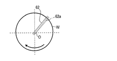
46,62 2流体ノズル
48 移動機構
50 チャック
52 アーム
54 回転軸
60 パーティクル
Claims (6)
- 表面を下向きにして基板を水平に保持して回転させる基板保持機構と、
気体と液体との2流体ジェット流を前記基板保持機構で保持された基板の表面に向けて上向きに噴射する2流体ノズルとを有することを特徴とする基板洗浄装置。 - 前記基板保持機構の側方に立設した回転自在な支持軸と、この支持軸に基部を連結した水平方向に延びる揺動アームからなり、前記2流体ノズルを前記基板保持機構で保持された基板の表面と平行に移動させる移動機構とを更に有し、前記揺動アームの先端に前記2流体ノズルが取付けられていることを特徴とする請求項1に記載の基板洗浄装置。
- 前記揺動アームは、基板の中心からオフセットした洗浄開始位置から、基板の中心の下方位置を通って、基板の外周部外方の洗浄終了位置に、前記2流体ノズルを2流体ジェット流を噴出させつつ一方向に移動させるように構成されていることを特徴とする請求項2に記載の基板洗浄装置。
- 前記2流体ノズルは、前記基板保持機構で保持された基板の表面と平行に基板の直径方向に該基板の半径を跨って直線状に延び、基板の半径以上の長さのスリット状の噴射口を有するスリット型ノズルからなることを特徴とする請求項1に記載の基板洗浄装置。
- 表面を下向きにして基板を水平に回転させ、
水平に回転している基板の表面に向けて気体と液体との2流体ジェット流を2流体ノズルから上向きに噴射させることを特徴とする基板洗浄方法。 - 基板の中心からオフセットした洗浄開始位置から、基板の中心の下方位置を通って、基板の外周部外方の洗浄終了位置に、前記2流体ノズルを2流体ジェット流を噴出させつつ、基板の表面と平行に一方向に移動させることを特徴とする請求項5に記載の基板洗浄方法。
Priority Applications (4)
| Application Number | Priority Date | Filing Date | Title |
|---|---|---|---|
| JP2012287121A JP2014130883A (ja) | 2012-12-28 | 2012-12-28 | 基板洗浄装置及び基板洗浄方法 |
| KR1020130159803A KR20140086846A (ko) | 2012-12-28 | 2013-12-20 | 기판 세정 장치 및 기판 세정 방법 |
| TW102147709A TWI610359B (zh) | 2012-12-28 | 2013-12-23 | 基板洗淨裝置及基板洗淨方法 |
| US14/139,626 US20140182632A1 (en) | 2012-12-28 | 2013-12-23 | Substrate cleaning apparatus and substrate cleaning method |
Applications Claiming Priority (1)
| Application Number | Priority Date | Filing Date | Title |
|---|---|---|---|
| JP2012287121A JP2014130883A (ja) | 2012-12-28 | 2012-12-28 | 基板洗浄装置及び基板洗浄方法 |
Publications (2)
| Publication Number | Publication Date |
|---|---|
| JP2014130883A true JP2014130883A (ja) | 2014-07-10 |
| JP2014130883A5 JP2014130883A5 (ja) | 2015-08-27 |
Family
ID=51015749
Family Applications (1)
| Application Number | Title | Priority Date | Filing Date |
|---|---|---|---|
| JP2012287121A Pending JP2014130883A (ja) | 2012-12-28 | 2012-12-28 | 基板洗浄装置及び基板洗浄方法 |
Country Status (4)
| Country | Link |
|---|---|
| US (1) | US20140182632A1 (ja) |
| JP (1) | JP2014130883A (ja) |
| KR (1) | KR20140086846A (ja) |
| TW (1) | TWI610359B (ja) |
Cited By (2)
| Publication number | Priority date | Publication date | Assignee | Title |
|---|---|---|---|---|
| JP2018501665A (ja) * | 2015-07-13 | 2018-01-18 | ゼウス カンパニー リミテッド | 基板液処理装置及び方法 |
| JP2021015998A (ja) * | 2018-12-04 | 2021-02-12 | 株式会社ディスコ | ウエーハ洗浄装置 |
Families Citing this family (2)
| Publication number | Priority date | Publication date | Assignee | Title |
|---|---|---|---|---|
| CN107359107B (zh) * | 2014-11-18 | 2020-07-14 | 通富微电子股份有限公司 | 一种圆片清洗机用的喷头及圆片清洗机 |
| CN105826224B (zh) * | 2016-05-11 | 2019-05-21 | 中国电子科技集团公司第四十五研究所 | 一种用于半导体晶圆的清洁腔 |
Citations (4)
| Publication number | Priority date | Publication date | Assignee | Title |
|---|---|---|---|---|
| JP2001506061A (ja) * | 1997-09-24 | 2001-05-08 | アンテルユニヴェルシテール・ミクロ―エレクトロニカ・サントリュム・ヴェー・ゼッド・ドゥブルヴェ | 表面から液体を除去する方法及び装置 |
| JP2003517201A (ja) * | 1999-12-17 | 2003-05-20 | ナトゥール・インコーポレイテッド | 処理チャンバ、収納チャンバ、処理装置、並びに、処理方法。 |
| JP2005353739A (ja) * | 2004-06-09 | 2005-12-22 | Dainippon Screen Mfg Co Ltd | 基板洗浄装置 |
| JP2012204759A (ja) * | 2011-03-28 | 2012-10-22 | Toshiba Corp | 基板保持装置、基板洗浄装置および基板処理装置 |
Family Cites Families (4)
| Publication number | Priority date | Publication date | Assignee | Title |
|---|---|---|---|---|
| US5778554A (en) * | 1996-07-15 | 1998-07-14 | Oliver Design, Inc. | Wafer spin dryer and method of drying a wafer |
| KR100523635B1 (ko) * | 2003-02-04 | 2005-10-25 | 동부아남반도체 주식회사 | 웨이퍼 표면의 슬러리 제거 장치 및 그 방법 |
| CN100501931C (zh) * | 2004-04-23 | 2009-06-17 | 东京毅力科创株式会社 | 基板清洗方法、基板清洗装置 |
| KR100940136B1 (ko) * | 2006-08-29 | 2010-02-03 | 다이닛뽕스크린 세이조오 가부시키가이샤 | 기판처리방법 및 기판처리장치 |
-
2012
- 2012-12-28 JP JP2012287121A patent/JP2014130883A/ja active Pending
-
2013
- 2013-12-20 KR KR1020130159803A patent/KR20140086846A/ko not_active Application Discontinuation
- 2013-12-23 US US14/139,626 patent/US20140182632A1/en not_active Abandoned
- 2013-12-23 TW TW102147709A patent/TWI610359B/zh active
Patent Citations (4)
| Publication number | Priority date | Publication date | Assignee | Title |
|---|---|---|---|---|
| JP2001506061A (ja) * | 1997-09-24 | 2001-05-08 | アンテルユニヴェルシテール・ミクロ―エレクトロニカ・サントリュム・ヴェー・ゼッド・ドゥブルヴェ | 表面から液体を除去する方法及び装置 |
| JP2003517201A (ja) * | 1999-12-17 | 2003-05-20 | ナトゥール・インコーポレイテッド | 処理チャンバ、収納チャンバ、処理装置、並びに、処理方法。 |
| JP2005353739A (ja) * | 2004-06-09 | 2005-12-22 | Dainippon Screen Mfg Co Ltd | 基板洗浄装置 |
| JP2012204759A (ja) * | 2011-03-28 | 2012-10-22 | Toshiba Corp | 基板保持装置、基板洗浄装置および基板処理装置 |
Cited By (3)
| Publication number | Priority date | Publication date | Assignee | Title |
|---|---|---|---|---|
| JP2018501665A (ja) * | 2015-07-13 | 2018-01-18 | ゼウス カンパニー リミテッド | 基板液処理装置及び方法 |
| JP2021015998A (ja) * | 2018-12-04 | 2021-02-12 | 株式会社ディスコ | ウエーハ洗浄装置 |
| JP7092847B2 (ja) | 2018-12-04 | 2022-06-28 | 株式会社ディスコ | ウエーハ洗浄装置 |
Also Published As
| Publication number | Publication date |
|---|---|
| TWI610359B (zh) | 2018-01-01 |
| KR20140086846A (ko) | 2014-07-08 |
| US20140182632A1 (en) | 2014-07-03 |
| TW201428842A (zh) | 2014-07-16 |
Similar Documents
| Publication | Publication Date | Title |
|---|---|---|
| JP6093569B2 (ja) | 基板洗浄装置 | |
| US11676827B2 (en) | Substrate cleaning apparatus, substrate cleaning method, substrate processing apparatus, and substrate drying apparatus | |
| US9142399B2 (en) | Substrate cleaning method | |
| KR102338647B1 (ko) | 기판 세정 장치 | |
| CN111589752B (zh) | 清洗装置 | |
| JP2014130883A (ja) | 基板洗浄装置及び基板洗浄方法 | |
| JP7290695B2 (ja) | 超音波洗浄装置および洗浄具のクリーニング装置 | |
| JP6297308B2 (ja) | 基板洗浄装置及び基板洗浄方法 | |
| US9640384B2 (en) | Substrate cleaning apparatus and substrate cleaning method | |
| JP7050875B2 (ja) | 基板洗浄装置 | |
| JP6339351B2 (ja) | 基板洗浄装置および基板処理装置 | |
| JP6934918B2 (ja) | 基板洗浄装置 | |
| JP6612176B2 (ja) | 基板洗浄装置 | |
| JP2017204495A (ja) | 基板洗浄装置 | |
| WO2016076303A1 (ja) | 基板洗浄装置 |
Legal Events
| Date | Code | Title | Description |
|---|---|---|---|
| A521 | Request for written amendment filed |
Free format text: JAPANESE INTERMEDIATE CODE: A523 Effective date: 20150708 |
|
| A621 | Written request for application examination |
Free format text: JAPANESE INTERMEDIATE CODE: A621 Effective date: 20150708 |
|
| A131 | Notification of reasons for refusal |
Free format text: JAPANESE INTERMEDIATE CODE: A131 Effective date: 20160823 |
|
| A977 | Report on retrieval |
Free format text: JAPANESE INTERMEDIATE CODE: A971007 Effective date: 20160824 |
|
| A601 | Written request for extension of time |
Free format text: JAPANESE INTERMEDIATE CODE: A601 Effective date: 20161019 |
|
| A02 | Decision of refusal |
Free format text: JAPANESE INTERMEDIATE CODE: A02 Effective date: 20170228 |