JP2014107459A - Semiconductor chip pickup device - Google Patents
Semiconductor chip pickup device Download PDFInfo
- Publication number
- JP2014107459A JP2014107459A JP2012260433A JP2012260433A JP2014107459A JP 2014107459 A JP2014107459 A JP 2014107459A JP 2012260433 A JP2012260433 A JP 2012260433A JP 2012260433 A JP2012260433 A JP 2012260433A JP 2014107459 A JP2014107459 A JP 2014107459A
- Authority
- JP
- Japan
- Prior art keywords
- semiconductor chip
- adhesive sheet
- support
- suction
- claw
- Prior art date
- Legal status (The legal status is an assumption and is not a legal conclusion. Google has not performed a legal analysis and makes no representation as to the accuracy of the status listed.)
- Pending
Links
Images


Abstract
Description
本発明は、粘着シートに貼られた半導体チップを粘着シートから取り外す半導体チップのピックアップ装置に関する。 The present invention relates to a semiconductor chip pickup device for removing a semiconductor chip attached to an adhesive sheet from the adhesive sheet.
半導体ウエハは粘着シートに貼り付けられた状態で、格子状に切断(ダイシング)されている。切断された個片は粘着シートに張り付いた状態で半導体チップとして半導体チップの実装工程に供給されている。実装工程では、まず、半導体チップを粘着シートからはがすために、半導体チップを吸着して粘着シートから引きはがすピックアップ方法が行われている(特許文献1)。また、半導体チップを粘着シートから爪で剥離させながらピックアップして吸引ノズルで保持するものなどがある(特許文献2)。 The semiconductor wafer is cut (diced) in a lattice shape in a state of being attached to an adhesive sheet. The cut pieces are attached to the semiconductor chip mounting process as semiconductor chips in a state of being stuck to the adhesive sheet. In the mounting process, first, in order to peel off the semiconductor chip from the adhesive sheet, a pick-up method for adsorbing the semiconductor chip and peeling it from the adhesive sheet is performed (Patent Document 1). Also, there is one that picks up a semiconductor chip from a pressure-sensitive adhesive sheet with a nail and holds it with a suction nozzle (Patent Document 2).
一方、半導体チップの薄板化が進んでおり、欠けや割れが起きやすい薄板化された半導体チップに、過度のストレスを加えることなく粘着シートから取り外すことが求められている。 On the other hand, thinning of a semiconductor chip is progressing, and it is required to remove a thinned semiconductor chip from an adhesive sheet without applying excessive stress to the thinned semiconductor chip that is likely to be chipped or cracked.
そこで、本発明の課題は、粘着シートに貼り付けられた半導体チップにダメージを与えず、確実に粘着シートから取り外すことが出来る半導体チップのピックアップ装置を提供することとする。 Accordingly, an object of the present invention is to provide a pickup device for a semiconductor chip that can be reliably removed from the adhesive sheet without damaging the semiconductor chip attached to the adhesive sheet.
上記課題を解決するために、請求項1に記載の発明は、
粘着シートに貼り付けられた半導体チップを粘着シートから取り外す半導体チップのピックアップ装置であって、
前記粘着シートの半導体チップの貼り付けられている面と反対側の面に密着するステージが、半導体チップを粘着シートと接触して支持する支持面を有する支持部と、粘着シートを吸引する複数の吸引孔を有した吸引面とから構成され、
前記支持部の支持面が、前記吸引面から突出した面を形成し、支持面には半導体チップの対角線上を移動し粘着シートを押し上げる爪と爪の移動する溝が備えられ、半導体チップの対角線に沿って所定の幅で支持面が配置されている半導体チップのピックアップ装置である。
In order to solve the above-mentioned problem, the invention described in
A semiconductor chip pickup device for removing a semiconductor chip attached to an adhesive sheet from the adhesive sheet,
A stage that is in close contact with the surface of the pressure-sensitive adhesive sheet that is opposite to the surface on which the semiconductor chip is attached has a support portion that has a support surface that supports the semiconductor chip in contact with the pressure-sensitive adhesive sheet, and a plurality of pressure-sensitive adhesive sheets A suction surface having a suction hole,
The support surface of the support portion forms a surface protruding from the suction surface, and the support surface is provided with a claw for moving on the diagonal line of the semiconductor chip and pushing up the adhesive sheet, and a groove for moving the claw. A pickup device for a semiconductor chip in which a support surface is arranged with a predetermined width along the line.
半導体チップを粘着シートから取り外す際、半導体チップの角部から内側に向かって半導体チップの対角線上を爪が移動する。爪の移動にともない粘着シートと半導体チップは角部から剥離していく。半導体チップは爪の移動方向に沿って所定の幅で支持部の支持面で支持されており、支持部の外枠は窪み、吸引面となっている。このような構成のため爪の動作方向と平行なエッジが支持部の外枠で形成され、粘着シートの剥離方向が爪の動作方向と直角に近くなる。そのため、粘着シートから剥離する際に作用する応力が爪の移動の際、ほぼ均一となるため剥離が容易となり、半導体チップにダメージを与えず、確実に粘着シートから取り外すことが出来る。 When removing the semiconductor chip from the adhesive sheet, the claws move on the diagonal line of the semiconductor chip inward from the corner of the semiconductor chip. As the nail moves, the adhesive sheet and the semiconductor chip are peeled off from the corners. The semiconductor chip is supported by the support surface of the support portion with a predetermined width along the moving direction of the claw, and the outer frame of the support portion is recessed and becomes a suction surface. Due to such a configuration, an edge parallel to the operation direction of the nail is formed by the outer frame of the support portion, and the peeling direction of the adhesive sheet is close to a right angle with the operation direction of the nail. Therefore, the stress acting when peeling from the pressure-sensitive adhesive sheet becomes almost uniform when the nail moves, so that peeling becomes easy, and the semiconductor chip can be reliably removed without damaging the semiconductor chip.
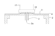
本発明の実施の形態について図面を参照して説明する。図1は本発明のピックアップ装置1の側面図である。図1において、左右方向をX軸、前後方向をY軸、X軸とY軸で構成されるXY平面に直交する軸をZ軸(上下方向)、Z軸周りをθ軸とする。
Embodiments of the present invention will be described with reference to the drawings. FIG. 1 is a side view of a
ピックアップ装置1は、筐体2と、爪3と、吸引面4とから構成されている。筐体2は、略円筒形の中空形状をしており、内部に爪3を突出および水平移動する機構が備えられている。吸引面4は、筐体2の上部に位置し、半導体チップ10が貼り付けられた粘着シート11を下側から支持している。
The
図2に吸引面4の平面図を示す。吸引面4には、複数の吸引孔15が設けられている。個々の吸引孔15は略円形の穴で筐体2の内部を真空引きした際に、真空吸引孔として動作する。吸引面4の中央部には、半導体チップ10を粘着シート11を介して指示するチップ支持領域5が設けられている。チップ支持領域5は半導体チップ10の輪郭線に対して約0.5mm内側に入った領域となっている。チップ支持領域5は、爪3が移動する溝6と、粘着シート11を吸着する吸着溝7と、粘着シート11を介して半導体チップ10を支持する支持部8と、窪み部9と、中央爪用穴16とから構成されている。図3は、チップ支持領域5の拡大平面図である。点線で表示した部分は、粘着シート11を介して支持される半導体チップ10の外形を意味する。
FIG. 2 shows a plan view of the
溝6は、チップ支持領域5の対角線に沿って、4隅からそれぞれ2列づつ設けられている。溝6に沿って爪3がチップ支持領域5の4隅から中央に向けて移動する。溝6は、4隅が始点で中央部が終点となる。吸着溝7は、チップ支持領域5の各辺に沿って複数本、設けられている。対角線上に溝6が設けられているため、チップ支持領域5の中央に向かうに従って、吸着溝7の長さが短くなっている。吸着溝7は、筐体2の内部と通じており、上述の筐体2内部の真空引きにより、真空吸引溝として動作する。支持部8は、溝6から所定の幅で、チップ支持領域5の各辺から中央に伸びる部分を指す。隣り合う支持部8の外枠線8aと、隣り合う半導体チップ10の角部を結んだ線で囲まれる領域を窪み部9と呼び、支持部8に比べて約0.1mm窪んだ領域としている。窪み部9の高さと、吸引面4は同一の高さとなっている。従い、支持部8の支持面8bが、吸引面4より約0.1mmの厚みだけ高く形成されていることになる。支持面8bが、吸引面4から突出した面を形成している。
The
半導体チップ10を粘着シート11から取り外す動作を、図4〜図10を用いて説明する。図4は、X軸方向(側面側)から半導体チップ10、粘着シート11,筐体2,爪3,吸引面4を参照した図である。以降、図4〜10の参照方向は同様とする。
The operation | movement which removes the
まず、図4に示すように、対象となる半導体チップ10の下側にピックアップ装置1を配置する。粘着シート11と支持部8の支持面8bが接触する。吸引面4は、支持面8bより0.1mm低いため粘着シート11と接触しない。
First, as shown in FIG. 4, the
次に、図5に示すように、筐体2の内部を図示していない真空ポンプで吸引し、吸引面4と粘着シート11を吸着させる。チップ支持領域5が半導体チップ10の外形よりも0.5mm内側に形成されているため、半導体チップ10の外周に張り付いている粘着シート11が支持面8bと吸引面4の段差の影響を受けて、剥離する。
Next, as shown in FIG. 5, the inside of the
次に、図6に示すように、半導体チップ10の中央に向けて下側から爪3を突出させる。半導体チップ10の角部10aが撓み、粘着シート11から剥がれ始める。
Next, as shown in FIG. 6, the
次に、図7に示すように、爪3を溝5に沿って半導体チップ10の内側に移動させる。爪3の移動にともない、半導体チップ10と粘着シート11の剥離エリア12が広がる。
Next, as shown in FIG. 7, the
次に、図8に示すように、爪3が半導体チップ10の中央部まで移動する。
Next, as shown in FIG. 8, the
次に、図9に示すように、半導体チップ10の中央部に配置されていた中央爪3aが上昇する。
Next, as shown in FIG. 9, the
次に、図10に示すように、中央爪3aが上昇し、粘着シート11から剥離された半導体チップ10がコレット17に吸着されピックアップ動作が完了する。
Next, as shown in FIG. 10, the
図11にチップ支持領域5の爪3の移動方向と支持部8と窪み部9の関係を示す。説明の関係上、吸着溝7は表記しない。図11に示すように、爪3が溝6に沿って角部10aから矢印20aの方向に移動する。窪み部9がチップ支持部8に比べて低いため、爪3が半導体チップ10の角部10aから内側に移動する際に、粘着シート11から半導体チップ10が剥離するきっかけを作ることになる。支持部8は所定の幅で形成されており、外枠線8aは、爪3の移動方向と平行に位置している。そのため粘着シート11の剥離方向20bが爪3の移動方向と直角に近くなる。このような場合、粘着シート11と半導体チップ10に作用する剥離応力は、爪3の移動にともない、ほぼ均一になると考えられる。剥離応力が均一なため、剥離途中で半導体チップ10にダメージを与えることなく、容易に剥離することが出来る。
FIG. 11 shows the relationship between the movement direction of the
1 ピックアップ装置
2 筐体
3 爪
3a 中央爪
4 吸引面
5 チップ支持領域
6 溝
7 吸着溝
8 支持部
8b 支持面
9 窪み部
10 半導体チップ
11 粘着シート
12 剥離エリア
15 吸引孔
16 中央爪用穴
17 コレット
8a 外枠線
10a 角部
10b 線
20a 爪の移動方向
20b 剥離方向
DESCRIPTION OF
Claims (1)
前記粘着シートの半導体チップの貼り付けられている面と反対側の面に密着するステージが、半導体チップを粘着シートと接触して支持する支持面を有する支持部と、粘着シートを吸引する複数の吸引孔を有した吸引面とから構成され、
前記支持部の支持面が、前記吸引面から突出した面を形成し、支持面には半導体チップの対角線上を移動し粘着シートを押し上げる爪と爪の移動する溝が備えられ、半導体チップの対角線に沿って所定の幅で支持面が配置されている半導体チップのピックアップ装置。 A semiconductor chip pickup device for removing a semiconductor chip attached to an adhesive sheet from the adhesive sheet,
A stage that is in close contact with the surface of the pressure-sensitive adhesive sheet that is opposite to the surface on which the semiconductor chip is attached has a support portion that has a support surface that supports the semiconductor chip in contact with the pressure-sensitive adhesive sheet, and a plurality of pressure-sensitive adhesive sheets A suction surface having a suction hole,
The support surface of the support portion forms a surface protruding from the suction surface, and the support surface is provided with a claw for moving on the diagonal line of the semiconductor chip and pushing up the adhesive sheet, and a groove for moving the claw. A semiconductor chip pick-up device in which a support surface is arranged with a predetermined width along the surface.
Priority Applications (1)
| Application Number | Priority Date | Filing Date | Title |
|---|---|---|---|
| JP2012260433A JP2014107459A (en) | 2012-11-29 | 2012-11-29 | Semiconductor chip pickup device |
Applications Claiming Priority (1)
| Application Number | Priority Date | Filing Date | Title |
|---|---|---|---|
| JP2012260433A JP2014107459A (en) | 2012-11-29 | 2012-11-29 | Semiconductor chip pickup device |
Publications (1)
| Publication Number | Publication Date |
|---|---|
| JP2014107459A true JP2014107459A (en) | 2014-06-09 |
Family
ID=51028677
Family Applications (1)
| Application Number | Title | Priority Date | Filing Date |
|---|---|---|---|
| JP2012260433A Pending JP2014107459A (en) | 2012-11-29 | 2012-11-29 | Semiconductor chip pickup device |
Country Status (1)
| Country | Link |
|---|---|
| JP (1) | JP2014107459A (en) |
Cited By (1)
| Publication number | Priority date | Publication date | Assignee | Title |
|---|---|---|---|---|
| JP2019140232A (en) * | 2018-02-09 | 2019-08-22 | トヨタ自動車株式会社 | Peeling device |
-
2012
- 2012-11-29 JP JP2012260433A patent/JP2014107459A/en active Pending
Cited By (1)
| Publication number | Priority date | Publication date | Assignee | Title |
|---|---|---|---|---|
| JP2019140232A (en) * | 2018-02-09 | 2019-08-22 | トヨタ自動車株式会社 | Peeling device |
Similar Documents
| Publication | Publication Date | Title |
|---|---|---|
| KR101596461B1 (en) | Apparatus and Method for Chip Detaching | |
| JP4803751B2 (en) | Wafer protective tape peeling device | |
| JP6128459B2 (en) | Method for peeling a semiconductor chip from a metal foil | |
| JP2005175384A (en) | Sticking method and peeling method of masking tape | |
| JP2009188157A (en) | Chip-releasing device, chip-releasing method, and chip-pickup device | |
| JP2019041051A (en) | Adhesive tape peeling method and adhesive tape peeling device | |
| JP2006319150A (en) | Semiconductor chip pick-up device and method therefor | |
| JP2007103826A (en) | Pickup device for semiconductor chip | |
| TWI588928B (en) | Die pick-up method | |
| TWI790557B (en) | Support device for supporting a substrate, method of processing a substrate and semiconductor substrate | |
| JP6366223B2 (en) | Semiconductor chip pickup device | |
| JP2014107459A (en) | Semiconductor chip pickup device | |
| JP2008109119A (en) | Pickup apparatus and pickup method | |
| JP4816598B2 (en) | Chip peeling device, chip peeling method, and chip pickup device | |
| JP2005302932A (en) | Chip separation apparatus | |
| JP2004031672A (en) | Pickup device for chip | |
| JP2016219573A (en) | Pickup apparatus and method | |
| KR101669539B1 (en) | Substrate Separation Method and Device | |
| JP2008270417A (en) | Device and method for manufacturing semiconductor device | |
| KR101513226B1 (en) | Method for picking-up semiconductor chip using low frequency vibration | |
| JP2014165301A (en) | Pick-up device for semiconductor chip | |
| JP2010087359A (en) | Pickup apparatus | |
| KR20160006790A (en) | Semiconductor-chip pickup device | |
| JP2004259811A (en) | Die pick-up method and device | |
| JP2013004697A (en) | Manufacturing apparatus and manufacturing method for semiconductor device |