JP2014107448A - Laminated semiconductor device manufacturing method and laminated semiconductor manufacturing apparatus - Google Patents
Laminated semiconductor device manufacturing method and laminated semiconductor manufacturing apparatus Download PDFInfo
- Publication number
- JP2014107448A JP2014107448A JP2012260135A JP2012260135A JP2014107448A JP 2014107448 A JP2014107448 A JP 2014107448A JP 2012260135 A JP2012260135 A JP 2012260135A JP 2012260135 A JP2012260135 A JP 2012260135A JP 2014107448 A JP2014107448 A JP 2014107448A
- Authority
- JP
- Japan
- Prior art keywords
- substrate
- light receiving
- processing
- semiconductor device
- manufacturing
- Prior art date
- Legal status (The legal status is an assumption and is not a legal conclusion. Google has not performed a legal analysis and makes no representation as to the accuracy of the status listed.)
- Pending
Links
- 239000004065 semiconductor Substances 0.000 title claims abstract description 55
- 238000004519 manufacturing process Methods 0.000 title claims abstract description 32
- 239000000758 substrate Substances 0.000 claims abstract description 305
- 238000000034 method Methods 0.000 claims abstract description 47
- 238000010030 laminating Methods 0.000 claims abstract description 16
- 238000000137 annealing Methods 0.000 claims description 13
- 238000005498 polishing Methods 0.000 claims description 13
- 238000005530 etching Methods 0.000 claims description 5
- 238000003475 lamination Methods 0.000 abstract description 5
- 239000010410 layer Substances 0.000 description 58
- 239000000463 material Substances 0.000 description 12
- 230000005669 field effect Effects 0.000 description 7
- 239000000126 substance Substances 0.000 description 6
- RYGMFSIKBFXOCR-UHFFFAOYSA-N Copper Chemical compound [Cu] RYGMFSIKBFXOCR-UHFFFAOYSA-N 0.000 description 4
- XUIMIQQOPSSXEZ-UHFFFAOYSA-N Silicon Chemical compound [Si] XUIMIQQOPSSXEZ-UHFFFAOYSA-N 0.000 description 4
- 229910052802 copper Inorganic materials 0.000 description 4
- 239000010949 copper Substances 0.000 description 4
- 239000013078 crystal Substances 0.000 description 4
- 229910052710 silicon Inorganic materials 0.000 description 4
- 239000010703 silicon Substances 0.000 description 4
- 229910000679 solder Inorganic materials 0.000 description 4
- 239000000428 dust Substances 0.000 description 3
- 239000011810 insulating material Substances 0.000 description 3
- 239000011229 interlayer Substances 0.000 description 3
- 230000015572 biosynthetic process Effects 0.000 description 2
- 238000006243 chemical reaction Methods 0.000 description 2
- 239000003086 colorant Substances 0.000 description 2
- 238000009792 diffusion process Methods 0.000 description 2
- 239000007769 metal material Substances 0.000 description 2
- 230000003287 optical effect Effects 0.000 description 2
- 239000011347 resin Substances 0.000 description 2
- 229920005989 resin Polymers 0.000 description 2
- WFKWXMTUELFFGS-UHFFFAOYSA-N tungsten Chemical compound [W] WFKWXMTUELFFGS-UHFFFAOYSA-N 0.000 description 2
- 229910052721 tungsten Inorganic materials 0.000 description 2
- 239000010937 tungsten Substances 0.000 description 2
- VYPSYNLAJGMNEJ-UHFFFAOYSA-N Silicium dioxide Chemical compound O=[Si]=O VYPSYNLAJGMNEJ-UHFFFAOYSA-N 0.000 description 1
- RTAQQCXQSZGOHL-UHFFFAOYSA-N Titanium Chemical compound [Ti] RTAQQCXQSZGOHL-UHFFFAOYSA-N 0.000 description 1
- 229910052782 aluminium Inorganic materials 0.000 description 1
- XAGFODPZIPBFFR-UHFFFAOYSA-N aluminium Chemical compound [Al] XAGFODPZIPBFFR-UHFFFAOYSA-N 0.000 description 1
- 230000003321 amplification Effects 0.000 description 1
- 238000003486 chemical etching Methods 0.000 description 1
- 230000000295 complement effect Effects 0.000 description 1
- 150000001875 compounds Chemical class 0.000 description 1
- 238000000151 deposition Methods 0.000 description 1
- 230000009977 dual effect Effects 0.000 description 1
- 238000005286 illumination Methods 0.000 description 1
- 230000010354 integration Effects 0.000 description 1
- 239000011159 matrix material Substances 0.000 description 1
- 238000002844 melting Methods 0.000 description 1
- 230000008018 melting Effects 0.000 description 1
- 238000012986 modification Methods 0.000 description 1
- 230000004048 modification Effects 0.000 description 1
- 238000003199 nucleic acid amplification method Methods 0.000 description 1
- 229920002120 photoresistant polymer Polymers 0.000 description 1
- 238000005240 physical vapour deposition Methods 0.000 description 1
- 239000000049 pigment Substances 0.000 description 1
- 238000005268 plasma chemical vapour deposition Methods 0.000 description 1
- 229920001721 polyimide Polymers 0.000 description 1
- 239000009719 polyimide resin Substances 0.000 description 1
- 238000003825 pressing Methods 0.000 description 1
- 229910052814 silicon oxide Inorganic materials 0.000 description 1
- 238000003860 storage Methods 0.000 description 1
- 230000001629 suppression Effects 0.000 description 1
- 239000010936 titanium Substances 0.000 description 1
- 229910052719 titanium Inorganic materials 0.000 description 1
- 238000007740 vapor deposition Methods 0.000 description 1
Images


Landscapes
- Solid State Image Pick-Up Elements (AREA)
Abstract
Description
本発明は、積層半導体装置の製造方法および積層半導体製造装置に関する。 The present invention relates to a method for manufacturing a stacked semiconductor device and a stacked semiconductor manufacturing device.
受光素子を含む基板と信号処理回路を含む基板とを積層して製造される積層半導体装置がある。
[先行技術文献]
[特許文献]
[特許文献1]特開2006−49361号公報
There is a stacked semiconductor device manufactured by stacking a substrate including a light receiving element and a substrate including a signal processing circuit.
[Prior art documents]
[Patent Literature]
[Patent Document 1] Japanese Patent Application Laid-Open No. 2006-49361
積層半導体装置は、例えば、基板の薄化段階において支持用のダミー基板を脱着する等の手順により工数が多くなるので生産性が低い。 The laminated semiconductor device is low in productivity because the number of man-hours is increased by, for example, a procedure of detaching a supporting dummy substrate in the substrate thinning stage.
本発明の第一態様においては、受光素子を含む受光回路を有する受光基板と、受光回路から受けた信号を処理する処理回路を有する処理基板とを積層して積層半導体装置を製造する方法であって、受光回路側の面と処理回路側の面とを向い合せて受光基板および処理基板を積層する異種基板積層段階と、異種基板積層段階よりも後に受光基板を薄化する受光基板薄化段階とを備える積層半導体装置製造方法が提供される。 According to a first aspect of the present invention, there is provided a method of manufacturing a laminated semiconductor device by laminating a light receiving substrate having a light receiving circuit including a light receiving element and a processing substrate having a processing circuit for processing a signal received from the light receiving circuit. A heterogeneous substrate stacking step in which the light receiving substrate side and the processing circuit side surface face each other, and a light receiving substrate thinning step in which the light receiving substrate is thinned after the heterogeneous substrate stacking step. A method for manufacturing a stacked semiconductor device is provided.
本発明の第二態様においては、受光素子を含む受光回路を有する受光基板と、受光回路から受けた信号を処理する処理回路を有する処理基板とを積層して積層半導体装置を製造する装置であって、受光素子を含む受光回路を有する受光基板における受光回路側の面と受光回路から受けた信号を処理する処理回路を有する処理基板における処理回路側の面とを向い合せて受光基板および処理基板を積層する異種基板積層部と、異種基板積層部により処理基板に積層された受光基板において、受光基板を薄化する受光基板薄化部とを備える積層半導体製造装置が提供される。 In a second aspect of the present invention, there is provided an apparatus for manufacturing a laminated semiconductor device by laminating a light receiving substrate having a light receiving circuit including a light receiving element and a processing substrate having a processing circuit for processing a signal received from the light receiving circuit. The light receiving substrate and the processing substrate face each other with the light receiving circuit side surface of the light receiving substrate having the light receiving circuit including the light receiving element and the processing circuit side surface of the processing substrate having a processing circuit for processing a signal received from the light receiving circuit. There is provided a laminated semiconductor manufacturing apparatus comprising: a heterogeneous substrate laminating unit for laminating a semiconductor substrate; and a light receiving substrate laminated on a processing substrate by the heterogeneous substrate laminating unit, and a light receiving substrate thinning unit for thinning the light receiving substrate.
上記した発明の概要は、本発明の必要な特徴の全てを列挙したものではない。これら特徴群のサブコンビネーションも発明となり得る。 The above summary of the present invention does not enumerate all necessary features of the present invention. A sub-combination of these feature groups can also be an invention.
以下、発明の実施の形態を通じて本発明を説明する。下記の実施形態は特許請求の範囲に係る発明を限定するものではない。実施形態の中で説明されている特徴の組み合わせの全てが発明の解決手段に必須であるとは限らない。 Hereinafter, the present invention will be described through embodiments of the invention. The following embodiments do not limit the invention according to the claims. Not all combinations of features described in the embodiments are essential for the solution of the invention.
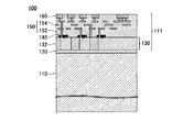
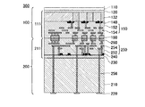
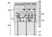
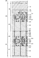
図1は、積層半導体装置400の材料として用い得る受光基板100の断面図である。受光基板100は、支持基板110、半導体ウェル130および多層配線層150を備える。
FIG. 1 is a cross-sectional view of a
支持基板110は、シリコン単結晶ウエハ等により形成され、受光基板100の機械的強度を担う厚さ、例えば、直径12インチのシリコン単結晶ウエハであれば、775μm程度の厚さを有する。支持基板110の一面には、絶縁層120を介して半導体ウェル130が配される。半導体ウェル130には、支持基板110の面方向に、複数のフォトダイオード132がマトリクス状に作り込まれている。
The
半導体ウェル130には、隣接して形成されたゲート電極140等により複数の電界効果トランジスタもが形成される。このような構造により、フォトダイオード132および電界効果トランジスタにより形成された受光回路111に対する支持基板110の浮遊容量が抑制され、受光回路111のスイッチング速度が向上されると共に消費電力が低減される。
A plurality of field effect transistors are also formed in the semiconductor well 130 by the
多層配線層150は、半導体ウェル130の表面に交互に積層された層間絶縁材152および配線材154により形成される。配線材154としては、チタン、タングステン等の金属材料を使用できる。
The
フォトダイオード132および電界効果トランジスタは、多層配線層150により相互に接続されて、概ね厚さ10μm以下の受光回路111を形成する。多層配線層150における配線材154の一端は、支持基板110と反対側の一面において外部に露出した接続パッド160に電気的に接続される。
The
受光回路111においては、フォトダイオード132の各々が画素に対応し、電界効果トランジスタが画素毎にリセット、選択および増幅を担う。フォトダイオード132が入射光を受けて蓄積した電荷は、電界効果トランジスタによるソースフォロワを通じて電圧信号として接続パッド160から外部に出力される。
In the
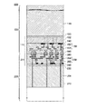
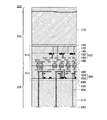
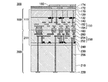
図2は、積層半導体装置400の材料として用い得る処理基板200の断面図である。処理基板200は、支持基板210、半導体ウェル230および多層配線層250を備える。
FIG. 2 is a cross-sectional view of a
支持基板210は、シリコン単結晶ウエハ等により形成され、受光基板100の機械的強度を担う厚さ、例えば、直径12インチのシリコン単結晶ウエハであれば、775μm程度の厚さを有する。支持基板210の一面には、半導体ウェル230が配される。半導体ウェル230には、半導体ウェル230に隣接して形成されたゲート電極240等により複数の電界効果トランジスタが作り込まれている。
The
多層配線層150は、半導体ウェル230の表面に交互に積層された層間絶縁材252および配線材254により形成される。複数の電界効果トランジスタは、多層配線層250により相互に接続されて処理回路211を形成する。
The
また、多層配線層250における配線材254の一端は、支持基板210と反対側の一面において外部に露出した接続パッド260に電気的に接続される。処理基板200の接続パッド260は、受光基板100の接続パッド160に接続される。これにより、処理基板200の処理回路211は、受光基板100の受光回路111の出力信号を処理する。処理回路211における処理としては、アナログ/デジタル変換、ノイズ抑圧、ファイル生成等を例示できる。
In addition, one end of the
なお、図示の処理基板200は、支持基板210に嵌入した貫通電極256を有する。貫通電極は、例えば、デュアルダマシン法により銅で形成される。貫通電極256の一端は、多層配線層250の配線材254に電気的に接続される。貫通電極256の他端は、図示の段階では、支持基板210の内部に埋没している。
The illustrated
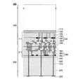
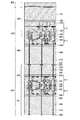
上記のような受光基板100および処理基板200を貼り合わせることにより、イメージセンサとして用い得る積層半導体装置400を製造できる。図3から図13は、そのような積層半導体装置400の製造過程を段階毎に示す断面図である。
By laminating the
なお、受光基板100および処理基板200のそれぞれは、図1または図2に示した構造をそれぞれの面方向に繰り返し有する。よって、受光基板100および処理基板200を積層することにより、多数の積層半導体装置400を含む積層基板300を一括して製造できる。
Each of the
まず、図3に示すように、受光基板100および処理基板200を積層して積層基板300を形成する。図示の例では、図1に示した状態に対して受光基板100の表裏を反転させ、処理基板200に積層する。これにより、この段階において1550μm以上の厚さを有する積層基板300が形成される。積層基板300においては、受光基板100の接続パッド160と、処理基板200の接続パッド260とが互いに当接して電気的に接続される。
First, as shown in FIG. 3, the
受光基板100および処理基板200は、接続パッド160、260の少なくとも一方をはんだバンプ、銅バンプ等にして圧接することにより貼り合わせてもよい。この場合、受光基板100および処理基板200はそれぞれ支持基板110、210を有しているので、十分な圧力を加えることができる。
The
また、接続パッド160、260を含む受光基板100および処理基板200の端面を鏡面研磨して常温接合させてもよい。この場合も、受光基板100および処理基板200が支持基板110、210を有しているので、これら支持基板110、210を保持して受光基板100および処理基板200を研磨することができる。
Further, the end surfaces of the
受光基板100および処理基板200の位置合わせは、予め定めた数箇所の位置合わせ指標の位置ずれに基づいて全体の位置ずれが最小になる位置を算出するグローバルアライメント法により、積層基板300の歩留りを向上させることができる。更に、位置合わせ指標の位置に基づいて、オフセット補正、回転補正、直交度補正、スケーリング補正等を加えて、位置合わせ精度をより向上させることかできる。
For the alignment of the
位置合わせ指標として、接続パッド160、260そのものを利用してもよいし、受光基板100および処理基板200に形成された配線、基板等を利用してもよい。更に、位置合わせに利用する目的で受光基板100および処理基板200に設けたアライメントマークを利用してもよい。また、位置ずれを測定するために位置合わせ指標を観察する場合、受光基板100および処理基板200の接合面を直接に観察する方法の他に、基板を透過する赤外帯域で観察してもよい。
As the alignment index, the
次に、図4に示すように、積層基板300において、処理基板200の支持基板210を、例えば500μm程度まで薄化する。支持基板210は、例えば、化学機械研磨により薄化できる。これにより、支持基板210の図中下面には、貫通電極256の端部が露出する。
Next, as shown in FIG. 4, in the
なお、処理基板200の薄化に先立って、200℃から300℃の温度範囲で、30分から60分の処理時間で積層基板300をアニール処理してもよい。これにより、受光基板100および処理基板200の貼り合わせに伴い積層基板300に生じた内部応力が緩和されるので、薄化のために研磨等で生じる応力により受光基板100および処理基板200が剥離することが防止される。
Prior to thinning of the
また、処理基板200の薄化処理後にも積層基板300を、上記と同様の条件でアニール処理してもよい。薄化処理後の支持基板210は平坦性が高いので、積層基板300を全体に均一に加熱できる。よって、アニール処理により緩和される内部応力も、積層基板300全体で均一になる。
In addition, the
次に、図5に示すように、支持基板210の図中下面に露出した貫通電極256の端部にバンプ220を形成する。これにより、処理基板200の処理回路211を、積層基板300の図中下面から外部に接続できる状態になる。バンプ220は、例えば、溶融はんだにより接合するはんだバンプ、相互拡散により接合する銅バンプ等を適宜選択できる。
Next, as shown in FIG. 5, bumps 220 are formed on the end portions of the through
次に、図6に示すように、受光基板100の支持基板110を薄化する。支持基板110は、例えば、処理基板200側に残る支持基板210を保持して化学機械研磨することにより薄化できる。ここで、図示の例では、支持基板110を全て除去せずに、絶縁層120が露出する直前で化学機械研磨を停止する。
Next, as shown in FIG. 6, the
ここまでの段階においては、受光基板100の表面が受光基板100の支持基板210により覆われている。よって、処理基板200側にける支持基板210の研磨、バンプ220の形成等により生じた塵芥は、受光基板100側の支持基板110に付着していたとしても、支持基板110の薄化処理と共に除去される。
In the steps so far, the surface of the
なお、上記のように受光基板100側の支持基板110を薄化する場合も、薄化処理の前後に、積層基板300をアニール処理してもよい。これにより、積層基板300の残留応力を緩和できる。また、薄化処理により生じた応力を開放できる。アニール処理は、200℃から300℃の温度範囲で、30分から60分の処理時間で有効になる。
Even when the
続いて、図7に示すように、絶縁層120の表面に残った支持基板110を化学エッチングにより除去する。エッチャントとして、支持基板110を食刻するが、絶縁層120とは反応しない選択性を有するものを用いる。これにより、積層基板300には、厚さ10μm程度の受光回路111が残る。これにより、支持基板110の除去後に形成される受光基板100の表面は、絶縁層120自体の平坦性を有する。このように、化学機械研磨で支持基板110を残し、エッチングにより支持基板110を除去することにより、化学機械研磨により生じがちな研磨量の偏りを防止できる。
Subsequently, as shown in FIG. 7, the
このように、上記の方法では、化学機械研磨をする場合に限って一時的に使用されるダミー基板を用いることなく薄化処理を実行して積層基板300を製造できる。よって、ダミー基板の着脱等の作業工数を省くことができ、積層基板の製造工程を簡略化できる。
Thus, in the above method, the
次に、図8に示すように、積層基板300における受光基板100側の表面に遮光層170を形成する。遮光層170は、受光基板100におけるフォトダイオード132の周囲に入射する入射光を遮断する。換言すれば、受光基板100において、フォトダイオード132が形成された領域に限って入射光を入射させる。
Next, as illustrated in FIG. 8, a
遮光層170は、例えばアルミニウム、タングステン等の金属材料を気相成長方により堆積させることにより形成できる。遮光層170の材料は、多層配線層150における配線材154と同じ材料であってもよい。ただし、遮光層170は、透過光を遮断できる厚さを有している。このように、フォトダイオード132に隣接して配することにより、遮光層170のパターン精度を向上させることができる。
The
このように、積層基板300を用いた場合は、受光基板100において支持基板110があった側からフォトダイオード132に光を入射させる裏面照射型イメージセンサが製造される。よって、以降の製造過程には、支持基板110が除去された跡に、入射光を透過させる層を形成する段階が含まれる。
As described above, when the
次に、図9に示すように、絶縁層120および遮光層170の表面に平坦化層172を形成する。平坦化層172は、プラズマCVD等の物理蒸着法により堆積したシリコン酸化膜により形成できる。
Next, as illustrated in FIG. 9, a
次に、図10に示すように、平坦化層172の表面に、有機平坦化層174を形成する。有機平坦化層174は、例えば、ポリイミド樹脂等を塗布することにより形成できる。これにより、受光基板100の入射側端面の平坦性を向上させると共に、次に説明する他の樹脂層の接着性を向上させる。
Next, as shown in FIG. 10, an
なお、有機平坦化層174の耐熱温度は、他の層を形成するSi化合物等に比較すると低い。よって、有機平坦化層174を形成した後の段階では、高温のアニール処理はできない。
Note that the heat resistance temperature of the
次に、図11に示すように、有機平坦化層174の表面に、オンチップカラーフィルタ180を形成する。オンチップカラーフィルタ180は、フォトダイオード132のそれぞれに対応して配される。また、オンチップカラーフィルタ180は、顔料を含むフォトレジスト材等により形成され、例えば赤、青および緑(原色系)またはシアン、マゼンタおよびイエロー(補色系)のいずれかに着色される。更に、オンチップカラーフィルタ180には、4色以上のフィルタが組み合わされる場合もある。
Next, as shown in FIG. 11, an on-
次に、図12に示すように、有機平坦化層174およびオンチップカラーフィルタ180の各表面を含む受光基板100の表面に、更に有機平坦化層182が形成される。これにより、オンチップカラーフィルタ180は、有機平坦化層174、182に埋設された状態になる。また、受光基板100の最表面は再び平坦化される。
Next, as shown in FIG. 12, an
次に、図13に示すように、有機平坦化層182の表面に、オンチップレンズ190が形成される。オンチップレンズ190は、有機樹脂により形成したレンズ材料層をエッチバック、リフロー等により加工してレンズ形状とすることにより形成される。オンチップレンズ190の各々は、中心が縁よりも厚い凸型レンズをなし、広い面積に入射した入射光をフォトダイオード132に集光する。尚、遮光層170、平坦化層172、有機平坦化層174、182、オンチップカラーフィルタ180、オンチップレンズ190は、これらの全てが必須なわけではなく、用途に応じて全部または一部を作成すればよい。
Next, as shown in FIG. 13, an on-
こうして、図13に示した断面構造を有する積層半導体装置400が完成する。積層半導体装置400は、受光基板100において支持基板110があった側から入射光が入射する裏面照射型イメージセンサである。フォトダイオード132への入射光により発生した電荷は、電圧信号として処理回路211に受け渡され、更に、デジタル変換等の処理を経て、バンプ220から外部に出力される。
Thus, the
積層半導体装置400が形成された積層基板300は、ダイシングにより切り分けられて多数のダイとなる。こうして得られたダイのそれぞれは、受光基板100および処理基板200を積層して製造したことにより、高い歩留りと高い集積密度とを兼ね備える。
The
なお、図7に示した状態から後に、遮光層170、オンチップカラーフィルタ180およびオンチップレンズ190のように光学的な機能を有する要素を受光基板100の表面に形成する場合には、マスク等を受光基板100に対して位置合わせする。この場合、絶縁層120、平坦化層172、有機平坦化層174、182を通じて見えるフォトダイオード132を、位置合わせ指標として利用してもよい。また、絶縁層120に、予めアライメントマークを形成しておいてもよい。更に、受光基板100を赤外帯域の照明光により観察して、多層配線層150の構造物を位置合わせ指標として利用してもよい。
When elements having an optical function such as the
図14は、他の積層基板301の断面図である。積層基板301は、図2に示した処理基板200と同じ構造を有する一対の処理基板201、202を、接続パッド260どうしが接合されるように積層して形成される。処理基板201、202の接合に係る位置合わせ指標、位置合わせ方法および接合方法については、図3を参照して説明した通りである。これにより、処理基板201の処理回路212と処理基板202の処理回路213とが相互に接続され、一体的な回路を形成する。
FIG. 14 is a cross-sectional view of another
次に、図15に示すように、積層基板301における一方の処理基板202の支持基板210を薄化処理し、支持基板210の表面に露出した貫通電極256の端面にバンプ220を形成する。薄化処理の方法とバンプ220の形成方法は、図4および図5を参照して説明した通りである。
Next, as shown in FIG. 15, the
次に、図16に示すように、図15に示した状態の積層基板301と、図5に示した状態の積層基板300とを接合して、積層基板302を形成する。積層基板301のバンプ220と積層基板302のバンプ220とは、銅バンプの相互拡散、はんだバンプの溶融等により接合できる。
Next, as illustrated in FIG. 16, the
こうして、積層基板300に含まれる受光回路111および処理回路211と、積層基板301における処理回路212、213とが、バンプ220および貫通電極256を通じて相互に結合される。これにより、積層基板302全体では、積層基板300の3倍に及ぶ大規模処理回路が形成される。
Thus, the
次に、図17に示すように、積層基板302の図中下端に位置する処理基板201の支持基板210を薄化処理し、支持基板210の表面に露出した貫通電極256の端面にバンプ220を形成する。薄化処理の方法とバンプ220の形成方法は、図4および図5を参照して説明した場合と同様である。こうして、積層基板302に形成された大規模処理回路は、図中最下段の処理基板201のバンプ220を通じて外部に出力できる状態になる。
Next, as shown in FIG. 17, the
次に、図18に示すように、薄化およびエッチングにより、積層基板302における受光基板100の支持基板110を除去する。支持基板110の薄化および除去は、図6および図7を参照して説明した通りである。
Next, as shown in FIG. 18, the
続いて、図19に示すように、受光基板100において露出した絶縁層120の上に、遮光層170、平坦化層172、有機平坦化層174、182、オンチップカラーフィルタ180およびオンチップレンズ190を順次形成して、積層半導体装置401を完成する。これら光学要素の形成過程は、図8から図13までを参照して説明した通りである。
Subsequently, as illustrated in FIG. 19, the
こうして製造された積層半導体装置401は、処理回路211、212、213を含む大規模処理回路を備えるので、アナログ/デジタル変換器に加えて、バッファ回路、記憶回路、プロセッサ等を一体的に備えたイメージセンサとすることができる。また、処理基板200、201、202を積層する過程では、受光基板100の受光面が支持基板110に覆われた状態なので、処理基板200、201、202の支持基板210の薄化処理等により生じた塵芥が受光基板100の表面に残留してイメージセンサとしての性能に影響を与えることが防止される。
Since the
なお、積層半導体装置401の製造過程においても、処理基板201、202の積層段階、積層基板300,301の積層段階のそれぞれの前後にアニール処理をしてもよい。しかしながら、個々の積層基板300、301を積層する段階ではアニール処理なしに低温で接合し、全ての基板が積層された後に一括してアニール処理してもよい。これにより、初期に積層された基板が繰り返しアニール処理の熱にさらされることが防止される。
Also in the manufacturing process of the
図20は、更に他の積層基板303の断面図である。積層基板303は、図5に示した状態の積層基板300に、複数の処理基板201を1枚ずつ順次積層して形成される。即ち、支持基板110を残した状態の積層基板300に対して、支持基板210を薄化する前の処理基板201を接合し、支持基板210を薄化し、バンプ220を形成する段階を繰り返すことにより、多層の積層基板303を形成できる。
FIG. 20 is a cross-sectional view of still another
上記のように、積層基板303の製造過程においては、処理基板201を1枚ずつ順次積層していくので、要求仕様に応じて任意の数の処理基板201を積層することができる。なお、図14から図16までに示したように予め作製した積層基板301を更に他の基板に積層する手順と、図20に示すように、処理基板201を一枚ずつ積層する手順とを混在させて、更に大規模な積層半導体装置を製造してもよい。
As described above, since the
また、この積層過程においては、受光基板100の受光面を支持基板110に覆った状態のまま、処理基板201の積層と薄化を繰り返すことができる。よって、処理基板201における支持基板210の薄化処理等により生じた塵芥が受光基板100の表面に残留してイメージセンサとしての性能に影響を与えることが防止される。
In this stacking process, the stacking and thinning of the
これにより、研磨等の薄化処理で一時的に使用されるダミー基板を用いることなく、多層の積層半導体装置を製造できる。よって、積層半導体装置を製造する場合の工数を低減できると共に、破棄されるダミー基板の消費を抑制できる。 Thereby, a multilayer laminated semiconductor device can be manufactured without using a dummy substrate temporarily used in a thinning process such as polishing. Therefore, it is possible to reduce the man-hour when manufacturing the laminated semiconductor device and to suppress the consumption of the discarded dummy substrate.
なお、上記のような積層基板303を作製する場合も、個々の積層段階ではアニール処理なしに低温で接合し、全ての基板が積層された後に一括してアニール処理してもよい。これにより、初期に積層された基板が繰り返しアニール処理の熱にさらされることが防止される。
Even when the
以上、本発明を実施の形態を用いて説明したが、本発明の技術的範囲は上記実施の形態に記載の範囲には限定されない。上記実施の形態に、多様な変更または改良を加えることが可能であることが当業者に明らかである。その様な変更または改良を加えた形態も本発明の技術的範囲に含まれ得ることが、特許請求の範囲の記載から明らかである。 As mentioned above, although this invention was demonstrated using embodiment, the technical scope of this invention is not limited to the range as described in the said embodiment. It will be apparent to those skilled in the art that various modifications or improvements can be added to the above-described embodiment. It is apparent from the scope of the claims that the embodiments added with such changes or improvements can be included in the technical scope of the present invention.
特許請求の範囲、明細書、および図面中において示した装置、システム、プログラム、および方法における動作、手順、ステップ、および段階等の各処理の実行順序は、特段「より前に」、「先立って」等と明示しておらず、また、前の処理の出力を後の処理で用いるのでない限り、任意の順序で実現しうることに留意すべきである。特許請求の範囲、明細書、および図面中の動作フローに関して、便宜上「まず、」、「次に、」等を用いて説明したとしても、この順で実施することが必須であることを意味するものではない。 The order of execution of each process such as operations, procedures, steps, and stages in the apparatus, system, program, and method shown in the claims, the description, and the drawings is particularly “before” or “prior to”. It should be noted that the output can be realized in any order unless the output of the previous process is used in the subsequent process. Regarding the operation flow in the claims, the description, and the drawings, even if it is described using “first”, “next”, etc. for convenience, it means that it is essential to carry out in this order. It is not a thing.
100 受光基板、110 支持基板、111 受光回路、120 絶縁層、130、230 半導体ウェル、132 フォトダイオード、140、240 ゲート電極、150、250 多層配線層、152、252 層間絶縁材、154、254 配線材、160、260 接続パッド、170 遮光層、172 平坦化層、174、182 有機平坦化層、180 オンチップカラーフィルタ、190 オンチップレンズ、200、201、202 処理基板、210 支持基板、211、212、213 処理回路、220 バンプ、256 貫通電極、300、301、302、303 積層基板、400、401 積層半導体装置 100 light receiving substrate, 110 supporting substrate, 111 light receiving circuit, 120 insulating layer, 130, 230 semiconductor well, 132 photodiode, 140, 240 gate electrode, 150, 250 multilayer wiring layer, 152, 252 interlayer insulating material, 154, 254 wiring Material, 160, 260 connection pad, 170 light shielding layer, 172 planarization layer, 174, 182 organic planarization layer, 180 on-chip color filter, 190 on-chip lens, 200, 201, 202 processing substrate, 210 support substrate, 211, 212, 213 processing circuit, 220 bump, 256 through electrode, 300, 301, 302, 303 laminated substrate, 400, 401 laminated semiconductor device
Claims (12)
前記受光回路側の面と前記処理回路側の面とを向い合せて前記受光基板および前記処理基板を積層する異種基板積層段階と、
前記異種基板積層段階よりも後に前記受光基板を薄化する受光基板薄化段階と
を備える積層半導体装置製造方法。 A manufacturing method for manufacturing a laminated semiconductor device by laminating a light receiving substrate having a light receiving circuit including a light receiving element and a processing substrate having a processing circuit for processing a signal received from the light receiving circuit,
A heterogeneous substrate stacking step of stacking the light receiving substrate and the processing substrate with the light receiving circuit side surface facing the processing circuit side surface;
A method for manufacturing a laminated semiconductor device, comprising: a light receiving substrate thinning step of thinning the light receiving substrate after the dissimilar substrate stacking step.
受光素子を含む受光回路を有する受光基板における前記受光回路側の面と前記受光回路から受けた信号を処理する処理回路を有する処理基板における前記処理回路側の面とを向い合せて前記受光基板および前記処理基板を積層する異種基板積層部と、
異種基板積層部により前記処理基板に積層された前記受光基板において、前記受光基板を薄化する受光基板薄化部と
を備える積層半導体製造装置。 A device for manufacturing a laminated semiconductor device by laminating a light receiving substrate having a light receiving circuit including a light receiving element and a processing substrate having a processing circuit for processing a signal received from the light receiving circuit,
A light receiving substrate having a light receiving circuit including a light receiving element, and a surface on the light receiving circuit side facing a surface on the processing circuit side of a processing substrate having a processing circuit for processing a signal received from the light receiving circuit; A heterogeneous substrate stacking unit for stacking the processing substrates;
A laminated semiconductor manufacturing apparatus, comprising: a light receiving substrate thinned portion for thinning the light receiving substrate in the light receiving substrate laminated on the processing substrate by a heterogeneous substrate laminated portion.
Priority Applications (1)
| Application Number | Priority Date | Filing Date | Title |
|---|---|---|---|
| JP2012260135A JP2014107448A (en) | 2012-11-28 | 2012-11-28 | Laminated semiconductor device manufacturing method and laminated semiconductor manufacturing apparatus |
Applications Claiming Priority (1)
| Application Number | Priority Date | Filing Date | Title |
|---|---|---|---|
| JP2012260135A JP2014107448A (en) | 2012-11-28 | 2012-11-28 | Laminated semiconductor device manufacturing method and laminated semiconductor manufacturing apparatus |
Publications (2)
| Publication Number | Publication Date |
|---|---|
| JP2014107448A true JP2014107448A (en) | 2014-06-09 |
| JP2014107448A5 JP2014107448A5 (en) | 2016-01-21 |
Family
ID=51028670
Family Applications (1)
| Application Number | Title | Priority Date | Filing Date |
|---|---|---|---|
| JP2012260135A Pending JP2014107448A (en) | 2012-11-28 | 2012-11-28 | Laminated semiconductor device manufacturing method and laminated semiconductor manufacturing apparatus |
Country Status (1)
| Country | Link |
|---|---|
| JP (1) | JP2014107448A (en) |
Cited By (12)
| Publication number | Priority date | Publication date | Assignee | Title |
|---|---|---|---|---|
| JP2017022207A (en) * | 2015-07-08 | 2017-01-26 | キヤノン株式会社 | Laminated solid-state imaging device |
| WO2017141103A1 (en) * | 2016-02-16 | 2017-08-24 | G-Ray Switzerland Sa | Structures, systems and methods for electrical charge transport across bonded interfaces |
| JP2018006561A (en) * | 2016-06-30 | 2018-01-11 | キヤノン株式会社 | Photoelectric conversion device and camera |
| JP2019068049A (en) * | 2017-09-29 | 2019-04-25 | 三星電子株式会社Samsung Electronics Co.,Ltd. | Image sensing device and manufacturing method thereof |
| JP2019140237A (en) * | 2018-02-09 | 2019-08-22 | キヤノン株式会社 | Photoelectric conversion device and imaging system |
| WO2019208359A1 (en) * | 2018-04-27 | 2019-10-31 | 東京エレクトロン株式会社 | Substrate processing system and substrate processing method |
| WO2020022015A1 (en) * | 2018-07-25 | 2020-01-30 | 株式会社ニコン | Joining method and joining device |
| JP2020065072A (en) * | 2016-03-31 | 2020-04-23 | 株式会社ニコン | Imaging element and imaging apparatus |
| WO2020121415A1 (en) * | 2018-12-11 | 2020-06-18 | ウルトラメモリ株式会社 | Method for manufacturing semiconductor module |
| JP2021184476A (en) * | 2014-07-31 | 2021-12-02 | 株式会社半導体エネルギー研究所 | Imaging device |
| WO2022158379A1 (en) * | 2021-01-22 | 2022-07-28 | キヤノン株式会社 | Photoelectric conversion device, photoelectric conversion system, and mobile body |
| WO2023131994A1 (en) * | 2022-01-05 | 2023-07-13 | キヤノン株式会社 | Photoelectric conversion device, photoelectric conversion system, and mobile body |
Citations (12)
| Publication number | Priority date | Publication date | Assignee | Title |
|---|---|---|---|---|
| JPH04287365A (en) * | 1991-03-15 | 1992-10-12 | Sony Corp | Manufacture of semiconductor device |
| JP2001339057A (en) * | 2000-05-30 | 2001-12-07 | Mitsumasa Koyanagi | Method of manufacturing three-dimensional image processor |
| JP2004168622A (en) * | 2002-11-22 | 2004-06-17 | Kyocera Corp | Single crystal sapphire substrate and its manufacturing method |
| JP2005353996A (en) * | 2004-06-14 | 2005-12-22 | Sony Corp | Solid-state imaging element and its manufacturing method, and semiconductor device and its manufacturing method |
| JP2006191081A (en) * | 2004-12-30 | 2006-07-20 | Magnachip Semiconductor Ltd | Image sensor in which light receiving region is extended and method of manufacturing the same |
| JP2007228460A (en) * | 2006-02-27 | 2007-09-06 | Mitsumasa Koyanagi | Stacked semiconductor device with integrated sensor mounted thereon |
| JP2009049081A (en) * | 2007-08-15 | 2009-03-05 | Nikon Corp | Bonding apparatus |
| WO2009123261A1 (en) * | 2008-04-01 | 2009-10-08 | 信越化学工業株式会社 | Method for producing soi substrate |
| US20110115004A1 (en) * | 2009-11-16 | 2011-05-19 | International Business Machines Corporation | Embedded photodetector apparatus in a 3d cmos chip stack |
| JP2011523779A (en) * | 2008-09-02 | 2011-08-18 | エス. オー. アイ. テック シリコン オン インシュレーター テクノロジーズ | Mixed trimming method |
| JP2012506206A (en) * | 2008-10-16 | 2012-03-08 | オムニヴィジョン テクノロジーズ インコーポレイテッド | Image sensor having a plurality of sensor layers, and operation and manufacturing method thereof |
| WO2012155152A1 (en) * | 2011-05-12 | 2012-11-15 | Olive Medical Corporation | Improved image sensor for endoscopic use |
-
2012
- 2012-11-28 JP JP2012260135A patent/JP2014107448A/en active Pending
Patent Citations (12)
| Publication number | Priority date | Publication date | Assignee | Title |
|---|---|---|---|---|
| JPH04287365A (en) * | 1991-03-15 | 1992-10-12 | Sony Corp | Manufacture of semiconductor device |
| JP2001339057A (en) * | 2000-05-30 | 2001-12-07 | Mitsumasa Koyanagi | Method of manufacturing three-dimensional image processor |
| JP2004168622A (en) * | 2002-11-22 | 2004-06-17 | Kyocera Corp | Single crystal sapphire substrate and its manufacturing method |
| JP2005353996A (en) * | 2004-06-14 | 2005-12-22 | Sony Corp | Solid-state imaging element and its manufacturing method, and semiconductor device and its manufacturing method |
| JP2006191081A (en) * | 2004-12-30 | 2006-07-20 | Magnachip Semiconductor Ltd | Image sensor in which light receiving region is extended and method of manufacturing the same |
| JP2007228460A (en) * | 2006-02-27 | 2007-09-06 | Mitsumasa Koyanagi | Stacked semiconductor device with integrated sensor mounted thereon |
| JP2009049081A (en) * | 2007-08-15 | 2009-03-05 | Nikon Corp | Bonding apparatus |
| WO2009123261A1 (en) * | 2008-04-01 | 2009-10-08 | 信越化学工業株式会社 | Method for producing soi substrate |
| JP2011523779A (en) * | 2008-09-02 | 2011-08-18 | エス. オー. アイ. テック シリコン オン インシュレーター テクノロジーズ | Mixed trimming method |
| JP2012506206A (en) * | 2008-10-16 | 2012-03-08 | オムニヴィジョン テクノロジーズ インコーポレイテッド | Image sensor having a plurality of sensor layers, and operation and manufacturing method thereof |
| US20110115004A1 (en) * | 2009-11-16 | 2011-05-19 | International Business Machines Corporation | Embedded photodetector apparatus in a 3d cmos chip stack |
| WO2012155152A1 (en) * | 2011-05-12 | 2012-11-15 | Olive Medical Corporation | Improved image sensor for endoscopic use |
Cited By (36)
| Publication number | Priority date | Publication date | Assignee | Title |
|---|---|---|---|---|
| JP2021184476A (en) * | 2014-07-31 | 2021-12-02 | 株式会社半導体エネルギー研究所 | Imaging device |
| JP2017022207A (en) * | 2015-07-08 | 2017-01-26 | キヤノン株式会社 | Laminated solid-state imaging device |
| WO2017141103A1 (en) * | 2016-02-16 | 2017-08-24 | G-Ray Switzerland Sa | Structures, systems and methods for electrical charge transport across bonded interfaces |
| TWI730053B (en) * | 2016-02-16 | 2021-06-11 | 瑞士商G射線瑞士公司 | Structures, systems and methods for electrical charge transport across bonded interfaces |
| US20190043914A1 (en) * | 2016-02-16 | 2019-02-07 | G-Ray Switzerland Sa | Structures, systems and methods for electrical charge transport across bonded interfaces |
| JP2019511834A (en) * | 2016-02-16 | 2019-04-25 | ジーレイ スイッツァーランド エスアー | Structures, systems and methods for charge transport across junction interfaces |
| US10985204B2 (en) | 2016-02-16 | 2021-04-20 | G-Ray Switzerland Sa | Structures, systems and methods for electrical charge transport across bonded interfaces |
| US11177312B2 (en) | 2016-03-31 | 2021-11-16 | Nikon Corporation | Image sensor and image capture device |
| US11682690B2 (en) | 2016-03-31 | 2023-06-20 | Nikon Corporation | Image sensor and image capture device |
| JP2020065072A (en) * | 2016-03-31 | 2020-04-23 | 株式会社ニコン | Imaging element and imaging apparatus |
| JP2022046686A (en) * | 2016-03-31 | 2022-03-23 | 株式会社ニコン | Imaging element and imaging apparatus |
| US20200258934A1 (en) | 2016-03-31 | 2020-08-13 | Nikon Corporation | Image sensor and image capture device |
| JP7191145B2 (en) | 2016-06-30 | 2022-12-16 | キヤノン株式会社 | Photoelectric conversion device, lamination substrate and camera |
| US10778920B2 (en) | 2016-06-30 | 2020-09-15 | Canon Kabushiki Kaisha | Photoelectric conversion apparatus and camera |
| JP2021108377A (en) * | 2016-06-30 | 2021-07-29 | キヤノン株式会社 | Photoelectric conversion device, substrate for lamination, and camera |
| US11637981B2 (en) | 2016-06-30 | 2023-04-25 | Canon Kabushiki Kaisha | Photoelectric conversion apparatus and camera |
| JP2018006561A (en) * | 2016-06-30 | 2018-01-11 | キヤノン株式会社 | Photoelectric conversion device and camera |
| US11482564B2 (en) | 2017-09-29 | 2022-10-25 | Samsung Electronics Co., Ltd. | Image sensing apparatus |
| JP2019068049A (en) * | 2017-09-29 | 2019-04-25 | 三星電子株式会社Samsung Electronics Co.,Ltd. | Image sensing device and manufacturing method thereof |
| JP2019140237A (en) * | 2018-02-09 | 2019-08-22 | キヤノン株式会社 | Photoelectric conversion device and imaging system |
| US11450523B2 (en) | 2018-04-27 | 2022-09-20 | Tokyo Electron Limited | Substrate processing system with eccentricity detection device and substrate processing method |
| JPWO2019208359A1 (en) * | 2018-04-27 | 2021-05-13 | 東京エレクトロン株式会社 | Board processing system and board processing method |
| CN112005341B (en) * | 2018-04-27 | 2024-01-09 | 东京毅力科创株式会社 | Substrate processing system and substrate processing method |
| JP7109537B2 (en) | 2018-04-27 | 2022-07-29 | 東京エレクトロン株式会社 | Substrate processing system and substrate processing method |
| WO2019208359A1 (en) * | 2018-04-27 | 2019-10-31 | 東京エレクトロン株式会社 | Substrate processing system and substrate processing method |
| CN112005341A (en) * | 2018-04-27 | 2020-11-27 | 东京毅力科创株式会社 | Substrate processing system and substrate processing method |
| KR102478503B1 (en) | 2018-07-25 | 2022-12-19 | 가부시키가이샤 니콘 | Bonding method and bonding device |
| JPWO2020022015A1 (en) * | 2018-07-25 | 2021-06-10 | 株式会社ニコン | Joining method and joining device |
| KR20210024078A (en) * | 2018-07-25 | 2021-03-04 | 가부시키가이샤 니콘 | Splicing method and splicing device |
| JP7147847B2 (en) | 2018-07-25 | 2022-10-05 | 株式会社ニコン | Joining method and joining apparatus |
| WO2020022015A1 (en) * | 2018-07-25 | 2020-01-30 | 株式会社ニコン | Joining method and joining device |
| JPWO2020121415A1 (en) * | 2018-12-11 | 2021-02-15 | ウルトラメモリ株式会社 | Manufacturing method of semiconductor module |
| WO2020121415A1 (en) * | 2018-12-11 | 2020-06-18 | ウルトラメモリ株式会社 | Method for manufacturing semiconductor module |
| CN113272938A (en) * | 2018-12-11 | 2021-08-17 | 超极存储器股份有限公司 | Method for manufacturing semiconductor module |
| WO2022158379A1 (en) * | 2021-01-22 | 2022-07-28 | キヤノン株式会社 | Photoelectric conversion device, photoelectric conversion system, and mobile body |
| WO2023131994A1 (en) * | 2022-01-05 | 2023-07-13 | キヤノン株式会社 | Photoelectric conversion device, photoelectric conversion system, and mobile body |
Similar Documents
| Publication | Publication Date | Title |
|---|---|---|
| JP2014107448A (en) | Laminated semiconductor device manufacturing method and laminated semiconductor manufacturing apparatus | |
| KR101351145B1 (en) | Cfa alignment mark formation in image sensors | |
| TWI508235B (en) | Chip package and method for forming the same | |
| TWI499047B (en) | Methods for forming a semiconductor device and imaging apparatus | |
| WO2013137049A1 (en) | Semiconductor device, semiconductor-device manufacturing method, semiconductor wafer, and electronic apparatus | |
| JP4915107B2 (en) | Solid-state imaging device and method for manufacturing solid-state imaging device | |
| JP2010118397A (en) | Camera module and process of manufacturing the same | |
| CN102856336A (en) | Chip package and method for forming the same | |
| JP2011035399A (en) | CMOS IMAGE SENSOR BIG VIA BONDING PAD APPLICATION FOR AlCu PROCESS | |
| JP2011146486A (en) | Optical device, method for manufacturing the same, and electronic apparatus | |
| US8829635B2 (en) | Solid-state imaging device, manufacturing method thereof, electronic apparatus, and semiconductor device | |
| TWI620284B (en) | Chip package and method for forming the same | |
| JP2012169489A (en) | Solid-state imaging device and method of manufacturing the same and electronic apparatus | |
| US9893116B2 (en) | Manufacturing method of electronic device and manufacturing method of semiconductor device | |
| CN102903763A (en) | Chip package and method for forming the same | |
| TWI442535B (en) | Electronics device package and fabrication method thereof | |
| CN104620385B (en) | Semiconductor device, the manufacturing method of semiconductor device and electronic device | |
| US8772136B2 (en) | Method for fabricating semiconductor device | |
| JP2015095517A (en) | Laminate type integrated circuit, and method for manufacturing the same | |
| JP2004063782A (en) | Solid-state image sensing device and its manufacturing method | |
| JP2011009389A (en) | Solid-state image pickup device and manufacturing method thereof | |
| JP2007059755A (en) | Solid-state imaging device and its manufacturing method | |
| US8318579B1 (en) | Method for fabricating semiconductor device | |
| JP6300662B2 (en) | Semiconductor device and manufacturing method of semiconductor device | |
| JP2022120579A (en) | Laminated semiconductor device and method for manufacturing the same |
Legal Events
| Date | Code | Title | Description |
|---|---|---|---|
| A521 | Request for written amendment filed |
Free format text: JAPANESE INTERMEDIATE CODE: A523 Effective date: 20151127 |
|
| A621 | Written request for application examination |
Free format text: JAPANESE INTERMEDIATE CODE: A621 Effective date: 20151127 |
|
| A977 | Report on retrieval |
Free format text: JAPANESE INTERMEDIATE CODE: A971007 Effective date: 20160907 |
|
| A131 | Notification of reasons for refusal |
Free format text: JAPANESE INTERMEDIATE CODE: A131 Effective date: 20161018 |
|
| A521 | Request for written amendment filed |
Free format text: JAPANESE INTERMEDIATE CODE: A523 Effective date: 20161214 |
|
| A02 | Decision of refusal |
Free format text: JAPANESE INTERMEDIATE CODE: A02 Effective date: 20170516 |
|
| A521 | Request for written amendment filed |
Free format text: JAPANESE INTERMEDIATE CODE: A523 Effective date: 20170809 |
|
| A911 | Transfer to examiner for re-examination before appeal (zenchi) |
Free format text: JAPANESE INTERMEDIATE CODE: A911 Effective date: 20170823 |
|
| A912 | Re-examination (zenchi) completed and case transferred to appeal board |
Free format text: JAPANESE INTERMEDIATE CODE: A912 Effective date: 20171102 |