JP2014033389A - Vibration device, electronic device, electronic apparatus, and movable body - Google Patents
Vibration device, electronic device, electronic apparatus, and movable body Download PDFInfo
- Publication number
- JP2014033389A JP2014033389A JP2012173749A JP2012173749A JP2014033389A JP 2014033389 A JP2014033389 A JP 2014033389A JP 2012173749 A JP2012173749 A JP 2012173749A JP 2012173749 A JP2012173749 A JP 2012173749A JP 2014033389 A JP2014033389 A JP 2014033389A
- Authority
- JP
- Japan
- Prior art keywords
- substrate
- vibration
- crystal oscillator
- package
- fixed
- Prior art date
- Legal status (The legal status is an assumption and is not a legal conclusion. Google has not performed a legal analysis and makes no representation as to the accuracy of the status listed.)
- Withdrawn
Links
Images


Classifications
-
- H—ELECTRICITY
- H03—ELECTRONIC CIRCUITRY
- H03B—GENERATION OF OSCILLATIONS, DIRECTLY OR BY FREQUENCY-CHANGING, BY CIRCUITS EMPLOYING ACTIVE ELEMENTS WHICH OPERATE IN A NON-SWITCHING MANNER; GENERATION OF NOISE BY SUCH CIRCUITS
- H03B1/00—Details
-
- H—ELECTRICITY
- H03—ELECTRONIC CIRCUITRY
- H03H—IMPEDANCE NETWORKS, e.g. RESONANT CIRCUITS; RESONATORS
- H03H9/00—Networks comprising electromechanical or electro-acoustic devices; Electromechanical resonators
- H03H9/02—Details
- H03H9/05—Holders; Supports
- H03H9/0538—Constructional combinations of supports or holders with electromechanical or other electronic elements
- H03H9/0547—Constructional combinations of supports or holders with electromechanical or other electronic elements consisting of a vertical arrangement
-
- H—ELECTRICITY
- H03—ELECTRONIC CIRCUITRY
- H03H—IMPEDANCE NETWORKS, e.g. RESONANT CIRCUITS; RESONATORS
- H03H9/00—Networks comprising electromechanical or electro-acoustic devices; Electromechanical resonators
- H03H9/02—Details
- H03H9/05—Holders; Supports
- H03H9/10—Mounting in enclosures
- H03H9/1007—Mounting in enclosures for bulk acoustic wave [BAW] devices
- H03H9/1014—Mounting in enclosures for bulk acoustic wave [BAW] devices the enclosure being defined by a frame built on a substrate and a cap, the frame having no mechanical contact with the BAW device
- H03H9/1021—Mounting in enclosures for bulk acoustic wave [BAW] devices the enclosure being defined by a frame built on a substrate and a cap, the frame having no mechanical contact with the BAW device the BAW device being of the cantilever type
Abstract
Description
本発明は、振動デバイス、それを用いた電子デバイス、電子機器、および移動体に関す
る。
The present invention relates to a vibration device, an electronic device using the vibration device, an electronic apparatus, and a moving body.
矩形状のICチップと、振動片と、を矩形状のベース(基板)に搭載した振動デバイス
としての水晶発振器が提案されている(例えば、特許文献1参照)。特許文献1に記載さ
れている水晶発振器では、ICチップの長辺側に接続端子が配置されており、その接続端
子をベースの短辺側に合わせて接続することでICチップがベースに搭載されている。加
えて、振動片は、ベースの長辺側の両端部に両端支持されており、ベースの実装端子もベ
ースの長辺側の両端部に設けられている。
A crystal oscillator has been proposed as a vibrating device in which a rectangular IC chip and a vibrating piece are mounted on a rectangular base (substrate) (see, for example, Patent Document 1). In the crystal oscillator described in
上述のような構成では、ベース(基板)に外力が加わった場合や実装基板とベースとの
熱膨張係数の違いなどによって、ベースに変形を生じる場合があるが、ベースの長辺側の
変形量が短辺側に比して大きくなる。上述の水晶発振器では、実装基板に固定される実装
端子、および振動片の両端支持がベースの長辺側に設けられているため、外力や熱膨張係
数の違いによるベースの変形の影響を受け易く、振動片に加わる応力によって振動特性に
変化を生じてしまうという課題を有していた。
In the configuration as described above, the base may be deformed when an external force is applied to the base (substrate) or due to a difference in thermal expansion coefficient between the mounting board and the base, but the deformation amount on the long side of the base Is larger than the short side. In the above-described crystal oscillator, the mounting terminal fixed to the mounting substrate and the both ends of the resonator element are provided on the long side of the base, so that it is easily affected by deformation of the base due to differences in external force and thermal expansion coefficient. Further, there is a problem that the vibration characteristics are changed by the stress applied to the resonator element.
本発明は、上述の課題の少なくとも一部を解決するためになされたものであり、以下の
形態または適用例として実現することが可能である。
SUMMARY An advantage of some aspects of the invention is to solve at least a part of the problems described above, and the invention can be implemented as the following forms or application examples.
[適用例1]本適用例に係る振動デバイスは、実装基板に固定される固定部と、自由端
と、平面視で前記固定部と自由端との間に接続部と、を有する基板と、前記接続部に片持
ち固定されている振動素子と、を含むことを特徴とする。
Application Example 1 A vibration device according to this application example includes a substrate having a fixed portion fixed to a mounting substrate, a free end, and a connection portion between the fixed portion and the free end in plan view, And a vibration element that is cantilevered to the connection portion.
本適用例によれば、固定部と離れた自由端側の基板に振動素子が片持ち固定されている
。このため、外力、あるいは加熱などによって実装基板が変形しても、基板においては固
定部に応力が集中し、自由端には応力が殆んど伝わらない。つまり、実装基板が変形した
場合でも、自由端側の接続部で基板に接続されている振動素子には、その応力が殆んど伝
わることが無く、振動素子の振動特性に変化が生じることを防止することができる。
According to this application example, the vibration element is cantilevered and fixed to the substrate on the free end side away from the fixing portion. For this reason, even if the mounting substrate is deformed by external force or heating, the stress is concentrated on the fixed portion of the substrate, and the stress is hardly transmitted to the free end. In other words, even when the mounting board is deformed, the stress is hardly transmitted to the vibration element connected to the board at the connection portion on the free end side, and the vibration characteristics of the vibration element change. Can be prevented.
[適用例2]上記適用例に記載の振動デバイスにおいて、前記固定部は、前記基板の一
辺に沿って設けられていることを特徴とする。
Application Example 2 In the vibrating device according to the application example described above, the fixing portion is provided along one side of the substrate.
本適用例によれば、固定部が基板の一辺に沿って設けられているため、自由端までの間
隔(距離)を大きくすることができるため、応力開放効果をさらに高めることが可能とな
る。したがって、固定部の受ける実装基板の変形応力の自由端への到達をさらに抑制する
ことができる。つまり、振動素子の特性への影響をさらに抑制することが可能となる。
According to this application example, since the fixing portion is provided along one side of the substrate, the distance (distance) to the free end can be increased, so that the stress release effect can be further enhanced. Therefore, it is possible to further suppress the deformation stress of the mounting substrate received by the fixed portion from reaching the free end. That is, it is possible to further suppress the influence on the characteristics of the vibration element.
[適用例3]上記適用例に記載の振動デバイスにおいて、前記基板を平面視して、前記
接続部の重心を通り前記自由端に直交する方向の第1の中心線と、前記固定部の重心を通
り前記自由端に直交する方向の第2の中心線と、がずれていることを特徴とする。
Application Example 3 In the vibration device according to the application example described above, when the substrate is viewed in plan, the first center line in a direction passing through the center of gravity of the connection portion and orthogonal to the free end, and the center of gravity of the fixing portion And a second center line in a direction perpendicular to the free end.
本適用例によれば、実装基板が変形した場合、基板の固定部の重心を通る第2の中心線
の部分の基板応力(基板の変形量)が大きくなるが、第1の中心線と、第2の中心線とが
ずれた位置に配置されているため、第1の中心線の通る振動素子の接続部の変形を固定部
の変形より小さくすることが可能となる。したがって、実装基板、あるいは基板の変形に
よる振動素子の特性への影響を抑制することが可能となる。
According to this application example, when the mounting substrate is deformed, the substrate stress (the amount of deformation of the substrate) of the portion of the second center line that passes through the center of gravity of the fixed portion of the substrate increases, but the first center line, Since the second center line is disposed at a position shifted from the second center line, the deformation of the connecting portion of the vibration element passing through the first center line can be made smaller than the deformation of the fixed portion. Therefore, it is possible to suppress the influence on the characteristics of the vibration element due to deformation of the mounting substrate or the substrate.
[適用例4]本適用例に係る電子デバイスは、上記適用例のいずれか一例に記載の振動
デバイスと、前記振動デバイスが片持ち固定された実装基板と、を含んでいることを特徴
とする。
Application Example 4 An electronic device according to this application example includes the vibration device according to any one of the application examples described above, and a mounting substrate on which the vibration device is cantilevered. .
本適用例によれば、実装基板に振動デバイスが片持ち固定されているため、実装基板の
変形の影響を振動デバイスが受け難い。さらに、用いている振動デバイスにおいても、上
述のように実装基板の変形の影響を受け難い構成であるため、実装基板の変形による特性
の変化を抑えた電子デバイスを提供することが可能となる。
According to this application example, since the vibration device is cantilevered on the mounting substrate, the vibration device is not easily affected by the deformation of the mounting substrate. Furthermore, since the vibration device used is also configured to be hardly affected by the deformation of the mounting substrate as described above, it is possible to provide an electronic device in which the change in characteristics due to the deformation of the mounting substrate is suppressed.
[適用例5]上記適用例に記載の電子デバイスにおいて、前記振動デバイスが樹脂で覆
われていることを特徴とする。
Application Example 5 In the electronic device according to the application example described above, the vibration device is covered with a resin.
本適用例によれば、振動デバイスを保護できる。また固定部を除く振動デバイスと実装
基板との間にも樹脂が入り込むため、実装基板に振動デバイスを固着できるとともに、樹
脂の可撓性により、実装基板の変形の影響を振動デバイスが受け難い。
According to this application example, the vibration device can be protected. In addition, since the resin enters between the vibration device excluding the fixing portion and the mounting substrate, the vibration device can be fixed to the mounting substrate, and the vibration device is not easily affected by the deformation of the mounting substrate due to the flexibility of the resin.
[適用例6]本適用例に係る電子機器は、上記適用例のいずれか一例に記載の振動デバ
イスが搭載されていることを特徴とする。
Application Example 6 An electronic apparatus according to this application example is characterized in that the vibration device according to any one of the application examples is mounted.
本適用例によれば、実装基板の変形の影響を受け難い振動デバイスを用いているため、
実装基板の変形による特性の変化を抑えた電子機器を提供することが可能となる。
According to this application example, since the vibration device that is not easily affected by the deformation of the mounting substrate is used,
It is possible to provide an electronic device in which a change in characteristics due to deformation of the mounting substrate is suppressed.
[適用例7]上記適用例に記載の電子機器において、前記振動デバイスと、前記振動デ
バイスが片持ち固定された実装基板と、を含むことを特徴とする。
Application Example 7 In the electronic apparatus according to the application example described above, the vibration device and a mounting substrate on which the vibration device is cantilevered are included.
本適用例によれば、実装基板に振動デバイスが片持ち固定されているため、実装基板の
変形の影響を振動デバイスが受け難い。さらに、用いている振動デバイスにおいても、上
述のように実装基板の変形の影響を受け難い構成であるため、実装基板の変形による特性
の変化を抑えた電子機器を提供することが可能となる。
According to this application example, since the vibration device is cantilevered on the mounting substrate, the vibration device is not easily affected by the deformation of the mounting substrate. Furthermore, since the vibration device used has a configuration that is hardly affected by the deformation of the mounting substrate as described above, it is possible to provide an electronic apparatus in which the change in characteristics due to the deformation of the mounting substrate is suppressed.
[適用例8]本適用例に係る移動体は、上記適用例のいずれか一例に記載の振動デバイ
スが搭載されていることを特徴とする。
Application Example 8 A moving body according to this application example includes the vibration device according to any one of the application examples described above.
本適用例によれば、実装基板の変形の影響を受け難い振動デバイスを用いているため、
実装基板の変形による特性の変化を抑えた移動体を提供することが可能となる。
According to this application example, since the vibration device that is not easily affected by the deformation of the mounting substrate is used,
It is possible to provide a moving body that suppresses changes in characteristics due to deformation of the mounting substrate.
以下、本発明に係る振動デバイスの実施形態を、図面を参照しながら第1実施形態、お
よび第2実施形態として説明する。
Hereinafter, embodiments of a vibration device according to the present invention will be described as a first embodiment and a second embodiment with reference to the drawings.
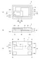
(振動デバイスの第1実施形態)
まず、本発明の第1実施形態に係る振動デバイスとしての水晶発振器について図1を用
いて説明する。図1は、第1実施形態に係る振動デバイスとしての水晶発振器の概略を示
し、(a)は平面図、(b)は(a)のQ1−Q1断面図、(c)は(a)の裏面図であ
る。なお、図1(a)は、説明を分かり易くするため蓋体を除いた状態を示している。
(First embodiment of vibration device)
First, a crystal oscillator as a vibrating device according to a first embodiment of the present invention will be described with reference to FIG. 1A and 1B schematically show a crystal oscillator as a vibrating device according to a first embodiment, wherein FIG. 1A is a plan view, FIG. 1B is a sectional view taken along line Q1-Q1 in FIG. 1A, and FIG. It is a back view. FIG. 1A shows a state in which the lid is removed for easy understanding of the description.
図1に示すように、振動デバイスとしての水晶発振器1は、パッケージ14の凹部に、
振動素子16と、電子部品としての半導体装置(ICチップ)15と、を収容し、パッケ
ージ14の開口部を蓋体19により密閉し、内部が気密に保持されている。
As shown in FIG. 1, the
The
[振動素子]
振動素子16は、基材(主要部分を構成する材料)を加工することにより一体に形成さ
れた振動片16bと、振動片16bの表裏の主面に設けられた励振電極16a(図示では
一方の主面のみ記載)とを有している。
[Vibration element]
The vibrating
本例の基材は水晶基板であり、水晶基板の圧電材料は三方晶系に属し、互いに直交する
結晶軸X、Y、Zを有する。X軸、Y軸、Z軸は、夫々電気軸、機械軸、光学軸と呼称さ
れる。そして水晶基板は、X−Z面をX軸の回りに所定の角度θだけ回転させた平面に沿
って、水晶から切り出された、所謂、回転Yカット水晶基板からなる平板が振動素子用と
して用いられる。
The base material of this example is a quartz substrate, and the piezoelectric material of the quartz substrate belongs to the trigonal system and has crystal axes X, Y, and Z orthogonal to each other. The X axis, the Y axis, and the Z axis are referred to as an electric axis, a mechanical axis, and an optical axis, respectively. The quartz substrate is a flat plate made of a so-called rotated Y-cut quartz substrate, which is cut from the quartz along a plane obtained by rotating the XZ plane around the X axis by a predetermined angle θ. It is done.
本実施形態では、X軸(電気軸)、Y軸(機械軸)、Z軸(光学軸)からなる直交座標
系のX軸を中心として、Z軸をY軸の−Y方向へ傾けた軸をZ’軸とし、Y軸をZ軸の+
Z方向へ傾けた軸をY’軸としたときに、X軸とZ’軸に平行な面で構成され、Y’軸に
平行な方向を厚みとするATカット水晶基板を用いている。また、ATカット水晶基板は
、Z’軸を含む面)が主面であり、厚みすべり振動が主振動として励振される。振動素子
16は、Y’軸に平行な方向を厚み方向として、X軸に平行な方向を長辺とし、Z’軸に
平行な方向を短辺とする矩形の形状を有する。
In the present embodiment, an axis in which the Z axis is inclined in the −Y direction of the Y axis with the X axis of the orthogonal coordinate system including the X axis (electrical axis), the Y axis (mechanical axis), and the Z axis (optical axis) as the center. Is the Z 'axis and the Y axis is the +
When an axis inclined in the Z direction is defined as a Y ′ axis, an AT-cut quartz substrate that is configured by a plane parallel to the X axis and the Z ′ axis and has a thickness parallel to the Y ′ axis is used. Further, the AT-cut quartz crystal substrate has a main surface (plane including the Z ′ axis), and thickness shear vibration is excited as the main vibration. The
なお、振動素子16は矩形状に限定されるものではなく、その他の四角形状であっても
よいし五角形以上の多角形、あるいは楕円、円を含む形状などでも良い。また、振動部の
一辺は、直線的なものに限定されず曲率を有するものであっても良いし、振動部の外形が
多角形の場合、前記一辺と接続される他の一辺との間の角部に別の辺が設けられていても
良い。また、本実施形態に係る振動素子は、ATカットに限定されるものではなく、厚み
すべり振動を励振するBTカット等の振動素子であってもよい。
Note that the
[パッケージ]
パッケージ14は、平板上の第1基板11と、第1基板11上に積層された枠状の第2
基板12と、第2基板12上に積層された枠状の第3基板13とを有し、半導体装置15
と振動素子16とが収容される凹部が形成されている。第1基板11、第2基板12、お
よび第3基板13は、例えばセラミックなどにより形成される。
[package]
The
The
And a recess in which the
第1基板11は、凹部側の半導体装置15が搭載される電子部品搭載面11aに、半導
体装置15が固定される接続電極(図示せず)が設けられている。半導体装置15に設け
られた複数の電極パッド(図示せず)と、電子部品搭載面11aに設けられた接続電極と
は、金バンプ18などにより接続されている。また、接続電極のいずれかは、パッケージ
14の図示しない内部配線により、第1基板11の外部底面に設けられた複数の外部接続
端子20a,20b,20c,21,22に電気的に接続されている。
In the
複数の外部接続端子20a,20b,20c,21,22の内の、第1基板11の一辺
に沿って並んでいる3つの外部接続端子20a,20b,20cは、水晶発振器1が実装
される図示しない実装基板への実装用端子である。なお、この3つの外部接続端子20a
,20b,20cが設けられている領域が水晶発振器1の固定部20である。他の外部接
続端子21,22は、実装基板への固定は行われない端子である。したがって、第1基板
11は、外部接続端子20a,20b,20cとして配置された固定部20で実装基板に
片持ち固定されている。片持ち固定とは、一箇所で水晶発振器1が固定され、水晶発振器
1の少なくとも一端が自由端となっている状態をいう。水晶発振器1では、他の外部接続
端子21,22が設けられている側の端は、実装基板に固定されない、所謂自由端となっ
ている。
Of the plurality of
, 20b, 20c is a fixed
なお、本実勢形態では、水晶発振器1の固定部20である3つの外部接続端子20a,
20b,20cが、第1基板11の一辺に沿って設けられている例で説明したが、固定部
20としての外部接続端子の配置はこれに限らない。例えば、外部接続端子の数は3以外
でもよい。さらに、外部接続端子は、必ずしも第1基板11の一辺に沿っていなくても、
一つの部位にまとまって固定部が構成されていればよく、その配置は問わない。
In this embodiment, the three
Although 20b and 20c were demonstrated in the example provided along one side of the 1st board |
The fixing part may be configured as a single unit, and the arrangement thereof is not limited.
第2基板12は、接続電極に接続される半導体装置15が収容可能な大きさの開口を有
する枠状の形状に形成されている。第2基板12上には、第2基板12の開口より広い開
口を有する第3基板13が積層され、固着されている。そして、そして第2基板12に第
3基板13が積層されて第3基板13の開口の内側に現れる第2基板面12aには、振動
素子16が接続されている。振動素子16は、第2基板面12aに形成された素子接続端
子(図示せず)に、振動素子16の接続電極(図示せず)を合わせて載置され、振動素子
16の接続部17において導電性接着剤17a,17bによって接着固定されている。
The
振動素子16は、外部接続端子20a,20b,20cが配置されている第1基板11
の固定部20と反対側である第1基板11の自由端14a側の、第2基板面12aに片持
ち固定されている。片持ち固定とは、一箇所で振動素子16が固定(固定端)され、振動
素子16の少なくとも一端が自由端となっている状態をいう。図1においては、振動素子
16における励振電極16aを挟んだ短辺方向を両端として、一方の端部が固定端となり
、他方の端部が自由端となっている。
すなわち、本実施形態では、振動素子16の自由端は、振動素子16の固定端よりも第
1基板11の固定部20に寄っているので、振動素子16の自由端から第1基板11の固
定部20までの応力の伝達経路を長くすることができる。
The
Is fixed to the
That is, in the present embodiment, the free end of the
また、振動素子16は、パッケージ14(第1基板11)を平面視したときに、振動素
子16の接続部17の重心P2を通り第1基板11の自由端(一辺)14aに直交する方
向に引かれた第1の中心線L2と、第1基板11の固定部20の重心P1を通り第1基板
11の自由端(一辺)14aに直交する方向に引かれた第2の中心線L1と、がずれてい
る位置に配置され、第2基板面12aの素子接続端子によって接着固定されている。
The
このような構成とすることで、実装基板が変形した場合、パッケージ14(第1基板1
1)の固定部20の重心P1を通る第2の中心線L1の部分の基板応力(基板の変形量)
が大きくなっても、第1の中心線L2と、第2の中心線L1と、がずれた位置に配置され
ているため、第1の中心線L2が通る振動素子16の接続部17の変形を、固定部20の
変形より小さくすることが可能となる。したがって、実装基板、あるいは第1基板11の
変形による振動素子16の特性への影響を少なくすることが可能となる。
With this configuration, when the mounting substrate is deformed, the package 14 (
1) Substrate stress (amount of deformation of the substrate) of the second center line L1 passing through the center of gravity P1 of the fixed
Since the first center line L2 and the second center line L1 are shifted from each other even when the first center line L2 is shifted, the deformation of the connecting
さらに、第3基板13の開口の上面13aに蓋体19が配置され、パッケージ14の開
口を封止し、パッケージ14の内部が気密封止され、水晶発振器1が得られる。
蓋体19は、例えば、42アロイ(鉄にニッケルが42%含有された合金)やコバール
(鉄、ニッケルおよびコバルトの合金)等の金属、セラミック、あるいはガラスなどを用
いて形成することができる。例えば、金属により蓋体19を形成した場合には、コバール
合金などを矩形環状に型抜きして形成されたシールリング(図示せず)を介してシーム溶
接することによりパッケージ14と接合される。パッケージ14および蓋体19によって
形成される凹部空間は、振動素子16が動作するための空間となるため、減圧空間または
不活性ガス雰囲気に密閉・封止することが好ましい。
Further, a
The
さらに、パッケージ14の4隅には、コーナーを凹状に形成して配線電極が設けられて
いる、所謂キャスタレーション23,24,25,26が設けられている。
Furthermore, so-called
上述の第1実施形態に係る水晶発振器1の効果について図1、および図3を参照して説
明する。図3は、振動デバイスとしての水晶発振器1の実装基板への実装状態を示す概略
の正面図であり、(a)は実装基板に変形が無い状態、(b)、(c)は実装基板に変形
が有る状態を示している。図1、および図3(a)に示すように、水晶発振器1は、固定
部20と離れた自由端14a側のパッケージ14(第2基板12)に振動素子16が片持
ち接続されて、実装基板70に片持ち固定されている。
したがって、図3(b)に示すように、外力、あるいは加熱などによって実装基板が実
装基板70aのように変形しても、パッケージ14(第1基板11)においては固定部2
0に応力が集中し、パッケージ14(第1基板11)の自由端14a側には応力が殆んど
伝わらない。なお、応力の発生状況のシミュレーション結果では、本実施形態の構成では
、従前の構成に比べて応力の発生が1/5程度になることが確認されている。つまり、実
装基板70aのように変形した場合でも、自由端14a側の接続部17で第2基板12に
接続されている振動素子16には、その応力が殆んど伝わることが無く、振動素子16の
振動特性の変化を防止することが可能となる。
The effect of the
Therefore, as shown in FIG. 3 (b), even if the mounting substrate is deformed like the mounting
Stress concentrates on 0, and almost no stress is transmitted to the
なお、図3(c)に示すように、固定部20がパッケージ14(第1基板11)の中央
部にある場合は、パッケージ14(第1基板11)の両端が自由端14a,14bとなる
。この構成において、図3(c)に示すように、実装基板70bが固定部20を中心に両
側に変形することがあっても、自由端14a,14bの部分は殆んど変形しないため、上
述と同様な効果を有している。
In addition, as shown in FIG.3 (c), when the fixing | fixed
なお、上述の説明では、パッケージ14の4隅にキャスタレーション23,24,25
,26が設けられている例で説明したが、キャスタレーションは、固定部20の設けられ
ているパッケージ14(第1基板11)の端側のキャスタレーション23,24は設けな
いことがより好ましい。これは、固定部20の設けられているパッケージ14(第1基板
11)の端側に隅部があることで、固定部20が溶融された半田などで実装基板に固定さ
れる際パッケージ14(第1基板11)の浮き上がりを防止する、所謂つっかい(突っ支
い)の役目を果たすことによる効果である。
In the above description,
However, it is more preferable that the castellation is not provided with the
(振動デバイスの第2実施形態)
次に、本発明の第2実施形態に係る振動デバイスとしての水晶発振器について図2を用
いて説明する。図2は、第2実施形態に係る振動デバイスとしての水晶発振器の概略を示
し、(a)は平面図、(b)は(a)のQ1−Q1断面図、(c)は(a)の裏面図であ
る。なお、図2(a)は、説明を分かり易くするため蓋体を除いた状態を示している。ま
た、本第2実施形態の説明では、上述の第1実施形態と同じ構成については詳細な説明を
省略することがある。
(Second embodiment of vibration device)
Next, a crystal oscillator as a vibrating device according to a second embodiment of the invention will be described with reference to FIG. 2A and 2B schematically show a crystal oscillator as a vibrating device according to the second embodiment, in which FIG. 2A is a plan view, FIG. 2B is a sectional view taken along line Q1-Q1 in FIG. 2A, and FIG. It is a back view. FIG. 2A shows a state where the lid is removed for easy understanding of the description. In the description of the second embodiment, detailed description of the same configuration as that of the first embodiment described above may be omitted.
図2に示すように、振動デバイスとしての水晶発振器2は、パッケージ34の凹部に、
振動素子36と、電子部品としての半導体装置(ICチップ)35と、を収容し、パッケ
ージ34の開口部を蓋体39により密閉し、内部が気密に保持されている。
As shown in FIG. 2, the
The
[振動素子]
振動素子36は、基材(主要部分を構成する材料)を加工することにより一体に形成さ
れた振動片36bと、振動片36bの表裏の主面に設けられた励振電極36a(図示では
一方の主面のみ記載)とを有している。なお、基材については第1実施形態と同様である
のでその説明を省略する。
[Vibration element]
The
[パッケージ]
パッケージ34は、平板上の第1基板31と、第1基板31上に積層された枠状の第2
基板32と、第2基板32上に積層された枠状の第3基板33とを有し、半導体装置35
と振動素子36とが収容される凹部が形成されている。第1基板31、第2基板32、お
よび第3基板33は、例えばセラミックなどにより形成される。
[package]
The
The
And a recess in which the
第1基板31は、凹部側の半導体装置35が搭載される電子部品搭載面31aに、半導
体装置35が固定される接続電極(図示せず)が設けられている。半導体装置35に設け
られた複数の電極パッド(図示せず)と、電子部品搭載面31aに設けられた接続電極と
は、金バンプ38などにより接続されている。また、接続電極のいずれかは、パッケージ
34の図示しない内部配線により、第1基板31の外部底面に設けられた複数の外部接続
端子40a,40b,40c,41,42に電気的に接続されている。
In the
複数の外部接続端子40a,40b,40c,41,42の内の、第1基板31の一辺
に沿って並んでいる3つの外部接続端子40a,40b,40cは、水晶発振器2が実装
される図示しない実装基板への実装用端子である。なお、この3つの外部接続端子40a
,40b,40cが設けられている領域が水晶発振器2の固定部40である。他の外部接
続端子41,42は、実装基板への固定は行われない端子である。したがって、第1基板
31は、外部接続端子40a,40b,40cとして配置された固定部40で実装基板に
片持ち固定され、他の外部接続端子41,42が設けられている側の端は、実装基板に固
定されない、所謂自由端となっている。
Of the plurality of
, 40b, 40c is a fixed
なお、本実施形態では、水晶発振器2の固定部40である3つの外部接続端子40a,
40b,40cが、第1基板31の一辺に沿って設けられている例で説明したが、固定部
40としての外部接続端子の配置はこれに限らない。例えば、外部接続端子の数は3つ以
外の数が設けられていてもよく、さらに、必ずしも第1基板31の一辺に沿っていなくて
も、一つの部位にまとまって固定部が構成されていればよく、外部接続端子の配置は問わ
ない。
In the present embodiment, three
Although 40b and 40c were demonstrated in the example provided along one side of the 1st board |
第2基板32は、接続電極に接続される半導体装置35が収容可能な大きさの開口を有
する枠状の形状に形成されている。第2基板32上には、第2基板32の開口より広い開
口を有する第3基板33が積層され、固着されている。そして、そして第2基板32に第
3基板33が積層されて第3基板33の開口の内側に現れる第2基板面32aには、振動
素子36が接続されている。振動素子36は、第2基板面32aに形成された素子接続端
子(図示せず)に、振動素子36の接続電極(図示せず)を合わせて載置され、振動素子
36の接続部37において導電性接着剤37a,37bによって接着固定される。
The
振動素子36は、外部接続端子40a,40b,40cが配置されている第1基板31
の固定部40と反対側である第1基板31の自由端34a側の、第2基板面32aに片持
ち接続で固定されている。
The
Is fixed to the
また、振動素子36は、パッケージ34(第1基板31)を平面視したときに、振動素
子36の接続部37の重心P4を通り、第1基板11の自由端(一辺)34aに直交する
方向に引かれた第1の中心線L4と、第1基板31の固定部40の重心P3を通り、第1
基板31の自由端(一辺)34aに直交する方向に引かれた第2の中心線L3と、がずれ
ている位置に配置され、第2基板面32aの素子接続端子によって接着固定されている。
In addition, the
The second center line L3 drawn in a direction perpendicular to the free end (one side) 34a of the
このような構成とすることで、実装基板が変形した場合、パッケージ34(第1基板3
1)の固定部40の重心P3を通る第2の中心線L3の部分の基板応力(基板の変形量)
が大きくなっても、第1の中心線L4と、第2の中心線L3とがずれた位置に配置されて
いるため、第1の中心線L4の通る振動素子36の接続部37の変形を固定部40の変形
より小さくすることが可能となる。したがって、実装基板、あるいは第1基板31の変形
による振動素子36の特性への影響を少なくすることが可能となる。
With this configuration, when the mounting substrate is deformed, the package 34 (
1) Substrate stress at the portion of the second center line L3 passing through the center of gravity P3 of the fixed portion 40 (the amount of deformation of the substrate).
Is increased, the first center line L4 and the second center line L3 are disposed at a position shifted from each other, so that the deformation of the connecting
さらに、第3基板33の開口の上面33aに蓋体39が配置され、パッケージ34の開
口を封止し、パッケージ34の内部が気密封止され、水晶発振器2が得られる。蓋体39
の構成、封止方法は、第1実施形態と同様であるので説明を省略する。パッケージ34、
および蓋体39によって形成される凹部空間は、振動素子36が動作するための空間とな
るため、減圧空間または不活性ガス雰囲気に密閉・封止することが好ましい。
Further, a
Since the configuration and the sealing method are the same as those in the first embodiment, description thereof is omitted.
Since the concave space formed by the
さらに、パッケージ34の4隅には、コーナーを凹状に形成して配線電極が設けられて
いる、所謂キャスタレーション43,44,45,46が設けられている。
Furthermore, so-called
上述の第2実施形態に係る水晶発振器2においても、上述の第1実施形態の水晶発振器
1と同様な効果を有している。即ち、固定部40と離れた自由端34a側のパッケージ3
4(第2基板32)に振動素子36が片持ち接続されて、実装基板(図示せず)に片持ち
固定されている。
したがって、外力、あるいは加熱などによって実装基板が変形しても、パッケージ34
(第1基板31)においては固定部40に応力が集中し、パッケージ34(第1基板31
)の自由端34a側には応力が殆んど伝わらない。なお、応力の発生状況のシミュレーシ
ョン結果では、本実施形態の構成では、従前の構成に比べて応力の発生が1/5程度にな
ることが確認されている。つまり、実装基板が変形した場合でも、自由端34a側の接続
部37で第2基板32に接続されている振動素子36には、その応力が殆んど伝わること
が無く、振動素子36の振動特性の変化を防止することが可能となる。また、固定部40
がパッケージ34(第1基板31)の中央部にある場合においても、上述の第1実施形態
の水晶発振器1と同様な効果を有している。
The
4 (second substrate 32) is cantilevered and is cantilevered to a mounting substrate (not shown).
Therefore, even if the mounting substrate is deformed by external force or heating, the
In the (first substrate 31), stress concentrates on the fixed
) Hardly transmits stress to the
Even in the center of the package 34 (first substrate 31), the same effect as the
なお、上述の説明では、パッケージ34の4隅にキャスタレーション43,44,45
,46が設けられている例で説明したが、キャスタレーションは、固定部40の設けられ
ているパッケージ34(第1基板31)の端側のキャスタレーション43,44は設けな
いことがより好ましい。これは、固定部40の設けられているパッケージ34(第1基板
31)の端側に隅部があることで、固定部40が溶融された半田などで実装基板に固定さ
れる際パッケージ34(第1基板31)の浮き上がりを防止する、所謂つっかい(突っ支
い)の役目を果たすことによる効果である。
In the above description,
However, it is more preferable that the castellation is not provided with the
(電子デバイス)
次に、本発明の一実施形態に係る振動デバイスとしての水晶発振器1を用いた電子デバ
イスの実施形態について図4を用いて説明する。図4は、電子デバイス一例としてのSI
Mカード(Subscriber Identity Module Card)の概略
を示す正断面図である。
(Electronic device)
Next, an embodiment of an electronic device using the
It is a front sectional view showing an outline of an M card (Subscriber Identity Module Card).
図4に示すように、電子デバイスの一例としてのSIMカード3は、導電配線53が形
成された実装基板50と、実装基板50上の導電配線53と接続固定された振動デバイス
としての水晶発振器1、および電子部品52とを有している。水晶発振器1は、実装基板
50上の導電配線53に、ハンダなどの接続材51によって片持ち支持で接続されている
。そして、外部との接続部分である導電配線53の一部を除く実装基板50上の導電配線
53、水晶発振器1、および電子部品52は、例えば、樹脂として、ポリ塩化ビニル(P
VC)、ポリエチレンテレフタレートグリコール(PET−G)などのコーティング材5
4で、オーバーコーティングされている。コーティング材54は、接続材51の部分を除
く水晶発振器1と実装基板50との間にも入り込んでおり、水晶発振器1と実装基板50
とを固着させている。また、コーティング材54は、ハンダなどの接続材51よりも軟ら
かく可撓性を有している。
As shown in FIG. 4, the
VC), polyethylene terephthalate glycol (PET-G) and other coating materials 5
4 is overcoated. The
And are fixed. The
このようなSIMカードは、携帯電話機に固有のID番号などを特定するために装着さ
れることが多く、小型薄型化が要求される。したがって、装着の際の脱着でSIMカード
の変形などを生じ易いため、本発明に係る振動デバイス(水晶発振器1)を用いた構成で
は、SIMカードの変形による振動デバイス(水晶発振器1)の特性変化を防止して安定
した動作を継続することが可能となる。
Such a SIM card is often mounted in order to specify an ID number unique to a mobile phone, and is required to be small and thin. Accordingly, since the SIM card is easily deformed by attachment / detachment during installation, in the configuration using the vibration device (crystal oscillator 1) according to the present invention, the characteristic change of the vibration device (crystal oscillator 1) due to the deformation of the SIM card. Can be prevented, and stable operation can be continued.
(電子機器)
次いで、本発明の一実施形態に係る振動デバイスとしての水晶発振器1,2、あるいは
電子デバイスを適用した電子機器について、図5〜図9に基づき、詳細に説明する。なお
、説明では、振動デバイスとしての水晶発振器1を用いた例を示している。
(Electronics)
Next, the
図5は、本発明の一実施形態に係る振動デバイスとしての水晶発振器1を備える電子機
器としての接触型ICカードの構成の概略を示し、(a)は実装基板側から見た平面図、
(b)はQ3−Q3断面図である。この図において、ICカード4は、実装基板60と、
実装基板60上に半田などの接合材61で片持ち固定された水晶発振器1と、実装基板6
0における水晶発振器1および電子部品64が固定された面側に設けられた外装部63を
備えている。接合材61の部分を除く実装基板60と水晶発振器1との間には、上記した
ような樹脂等のコーティング材54が設けられている。コーティング材54は、水晶発振
器1全体を覆うように設けられていてもよい。また、実装基板60における水晶発振器1
および電子部品64が固定された面の裏面には、電極62が設けられており、図示しない
導電配線によって電子部品64と導通している。
ICカード4は、水晶発振器1に内蔵されている図示しない半導体装置(ICチップ)
によって種々の情報が保持されており、カードリーダーを用いて情報の読み書きを行う。
FIG. 5 shows an outline of a configuration of a contact IC card as an electronic apparatus including a
(B) is Q3-Q3 sectional drawing. In this figure, the
The
The
An
The
A variety of information is held by the card reader, and information is read and written using a card reader.
図6は、本発明の一実施形態に係る水晶発振器1を備える電子機器としてのモバイル型
(又はノート型)のパーソナルコンピューターの構成の概略を示す斜視図である。この図
において、パーソナルコンピューター1100は、キーボード1102を備えた本体部1
104と、表示部100を備えた表示ユニット1106とにより構成され、表示ユニット
1106は、本体部1104に対しヒンジ構造部を介して回動可能に支持されている。こ
のようなパーソナルコンピューター1100には、水晶発振器1が内蔵されている。
FIG. 6 is a perspective view schematically showing a configuration of a mobile (or notebook) personal computer as an electronic apparatus including the
104 and a
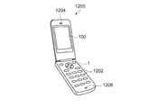
図7は、本発明の一実施形態に係る水晶発振器1を備える電子機器としての携帯電話機
(PHSも含む)の構成の概略を示す斜視図である。この図において、携帯電話機120
0は、複数の操作ボタン1202、受話口1204および送話口1206を備え、操作ボ
タン1202と受話口1204との間には、表示部100が配置されている。このような
携帯電話機1200には、水晶発振器1が内蔵されている。
FIG. 7 is a perspective view schematically showing a configuration of a mobile phone (including PHS) as an electronic apparatus including the
0 includes a plurality of
図8は、本発明の一実施形態に係る水晶発振器1を備える電子機器としてのデジタルス
チールカメラの構成の概略を示す斜視図である。なお、この図には、外部機器との接続に
ついても簡易的に示されている。ここで、従来のカメラは、被写体の光像により銀塩写真
フィルムを感光するのに対し、デジタルスチールカメラ1300は、被写体の光像をCC
D(Charge Coupled Device)等の撮像素子により光電変換して撮像信号(画像信号)を
生成する。
デジタルスチールカメラ1300におけるケース(ボディー)1302の背面には、表
示部100が設けられ、CCDによる撮像信号に基づいて表示を行う構成になっており、
表示部100は、被写体を電子画像として表示するファインダーとして機能する。また、
ケース1302の正面側(図中裏面側)には、光学レンズ(撮像光学系)やCCD等を含
む受光ユニット1304が設けられている。
撮影者が表示部100に表示された被写体像を確認し、シャッターボタン1306を押
下すると、その時点におけるCCDの撮像信号が、メモリー1308に転送・格納される
。また、このデジタルスチールカメラ1300においては、ケース1302の側面に、ビ
デオ信号出力端子1312と、データ通信用の入出力端子1314とが設けられている。
そして、図示されるように、ビデオ信号出力端子1312にはテレビモニター1430が
、データ通信用の入出力端子1314にはパーソナルコンピューター1440が、それぞ
れ必要に応じて接続される。さらに、所定の操作により、メモリー1308に格納された
撮像信号が、テレビモニター1430や、パーソナルコンピューター1440に出力され
る構成になっている。このようなデジタルスチールカメラ1300には、水晶発振器1が
内蔵されている。
FIG. 8 is a perspective view schematically showing a configuration of a digital still camera as an electronic apparatus including the
An image pickup signal (image signal) is generated through photoelectric conversion by an image pickup device such as D (Charge Coupled Device).
A
The
A
When the photographer confirms the subject image displayed on the
As shown in the figure, a
なお、本発明の一実施形態に係る水晶発振器1は、図6のパーソナルコンピューター(
モバイル型パーソナルコンピューター)、図7の携帯電話機、図8のデジタルスチールカ
メラの他にも、例えば、インクジェット式吐出装置(例えばインクジェットプリンター)
、ラップトップ型パーソナルコンピューター、テレビ、ビデオカメラ、ビデオテープレコ
ーダー、カーナビゲーション装置、ページャー、電子手帳(通信機能付も含む)、電子辞
書、電卓、電子ゲーム機器、ワードプロセッサー、ワークステーション、テレビ電話、防
犯用テレビモニター、電子双眼鏡、POS端末、医療機器(例えば電子体温計、血圧計、
血糖計、心電図計測装置、超音波診断装置、電子内視鏡)、魚群探知機、各種測定機器、
計器類(例えば、車両、航空機、船舶の計器類)、フライトシミュレーター等の電子機器
に適用することができる。
The
In addition to the mobile personal computer), the cellular phone shown in FIG. 7, and the digital still camera shown in FIG. 8, for example, an ink jet type ejection device (eg, an ink jet printer)
, Laptop personal computers, TVs, video cameras, video tape recorders, car navigation devices, pagers, electronic notebooks (including those with communication functions), electronic dictionaries, calculators, electronic game devices, word processors, workstations, videophones, crime prevention TV monitors, electronic binoculars, POS terminals, medical equipment (for example, electronic thermometers, blood pressure monitors,
Blood glucose meter, electrocardiogram measuring device, ultrasonic diagnostic device, electronic endoscope), fish detector, various measuring instruments,
The present invention can be applied to electronic devices such as instruments (for example, vehicle, aircraft, and ship instruments) and flight simulators.
(移動体)
図9は移動体の一例としての自動車を概略的に示す斜視図である。自動車106には本
発明に係る振動デバイスの一例としての水晶発振器1が搭載されている。例えば、同図に
示すように、移動体としての自動車106には、水晶発振器1を内蔵してタイヤ109な
どを制御する電子制御ユニット108が車体107に搭載されている。また、水晶発振器
1は、他にもキーレスエントリー、イモビライザー、カーナビゲーションシステム、カー
エアコン、アンチロックブレーキシステム(ABS)、エアバック、タイヤ・プレッシャ
ー・モニタリング・システム(TPMS:Tire Pressure Monitoring System)、エンジン
コントロール、ハイブリッド自動車や電気自動車の電池モニター、車体姿勢制御システム
、等の電子制御ユニット(ECU:electronic control unit)に広く適用できる。
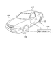
(Moving body)
FIG. 9 is a perspective view schematically showing an automobile as an example of a moving body. The
1,2…水晶発振器、3…電子デバイスとしてのSIMカード、4…電子機器としての
ICカード、11,31…第1基板、11a,31a…電子部品搭載面、12,32…第
2基板、12a,32a…第2基板面、13,33…第3基板、13a,33a…第3基
板の開口、14,34…パッケージ、14a,34a,14b…自由端(一辺)、15,
35…半導体装置、16,36…振動素子、16a,36a…励振電極、16b,36b
…振動片、17,37…接続部、17a,17b,37a,37b…導電性接着剤、18
,38…金バンプ、19,39…蓋体、20a,20b,20c,21,22…外部接続
端子、23,24,25,26…キャスタレーション、40a,40b,40c…外部接
続端子、43,44,45,46…キャスタレーション、106…移動体としての自動車
、1100…電子機器としてのモバイル型のパーソナルコンピューター、1200…電子
機器としての携帯電話機、1300…電子機器としてのデジタルスチールカメラ、P1,
P3…固定部の重心、P2,P4…接続部の重心、L1,L3…第2の中心線、L2,L
4…第1の中心線。
DESCRIPTION OF
35 ... Semiconductor device, 16, 36 ... Vibration element, 16a, 36a ... Excitation electrode, 16b, 36b
... Vibrating piece, 17, 37 ... Connection part, 17a, 17b, 37a, 37b ... Conductive adhesive, 18
, 38 ... Gold bumps, 19, 39 ... Lid, 20a, 20b, 20c, 21, 22 ... External connection terminals, 23, 24, 25, 26 ... Castellations, 40a, 40b, 40c ... External connection terminals, 43, 44, 45, 46 ... castellation, 106 ... automobile as mobile body, 1100 ... mobile personal computer as electronic device, 1200 ... mobile phone as electronic device, 1300 ... digital still camera as electronic device, P1,
P3: the center of gravity of the fixed part, P2, P4: the center of gravity of the connecting part, L1, L3: second center line, L2, L
4 ... 1st center line.
Claims (8)
部を有している基板と、
前記接続部に片持ち固定されている振動素子と、
を含むことを特徴とする振動デバイス。 A fixed portion fixed to the mounting substrate, a free end, and a substrate having a connection portion between the fixed portion and the free end in plan view;
A vibration element that is cantilevered to the connection part;
A vibrating device comprising:
前記固定部は、前記基板の一辺に沿って設けられていることを特徴とする振動デバイス
。 The vibrating device according to claim 1,
The vibration device, wherein the fixing portion is provided along one side of the substrate.
前記基板を平面視して、前記接続部の重心を通り前記自由端に直交する方向の第1の中
心線と、前記固定部の重心を通り前記自由端に直交する方向の第2の中心線と、がずれて
いることを特徴とする振動デバイス。 The vibrating device according to claim 1 or 2,
A first center line in a direction perpendicular to the free end passing through the center of gravity of the connecting portion and a second center line in a direction perpendicular to the free end passing through the center of gravity of the fixed portion when viewed in plan And a vibration device characterized by being displaced.
前記振動デバイスが片持ち固定されている実装基板と、
を含むことを特徴とする電子デバイス。 A vibrating device according to any one of claims 1 to 3,
A mounting substrate on which the vibration device is cantilevered; and
An electronic device comprising:
前記振動デバイスが樹脂で覆われていることを特徴とする電子デバイス。 The electronic device according to claim 4.
An electronic device, wherein the vibration device is covered with a resin.
特徴とする電子機器。 An electronic apparatus comprising the vibration device according to any one of claims 1 to 3.
前記振動デバイスと、
前記振動デバイスが片持ち固定されている実装基板と、
を含むことを特徴とする電子機器。 The electronic device according to claim 6,
The vibration device;
A mounting substrate on which the vibration device is cantilevered; and
An electronic device comprising:
特徴とする移動体。 A moving body on which the vibration device according to any one of claims 1 to 3 is mounted.
Priority Applications (3)
| Application Number | Priority Date | Filing Date | Title |
|---|---|---|---|
| JP2012173749A JP2014033389A (en) | 2012-08-06 | 2012-08-06 | Vibration device, electronic device, electronic apparatus, and movable body |
| US13/950,353 US20140035685A1 (en) | 2012-08-06 | 2013-07-25 | Resonator device, electronic device, electronic apparatus, and mobile object |
| CN201310335558.0A CN103580639A (en) | 2012-08-06 | 2013-08-05 | Resonator device, electronic device, electronic apparatus, and mobile object |
Applications Claiming Priority (1)
| Application Number | Priority Date | Filing Date | Title |
|---|---|---|---|
| JP2012173749A JP2014033389A (en) | 2012-08-06 | 2012-08-06 | Vibration device, electronic device, electronic apparatus, and movable body |
Publications (2)
| Publication Number | Publication Date |
|---|---|
| JP2014033389A true JP2014033389A (en) | 2014-02-20 |
| JP2014033389A5 JP2014033389A5 (en) | 2015-08-20 |
Family
ID=50024897
Family Applications (1)
| Application Number | Title | Priority Date | Filing Date |
|---|---|---|---|
| JP2012173749A Withdrawn JP2014033389A (en) | 2012-08-06 | 2012-08-06 | Vibration device, electronic device, electronic apparatus, and movable body |
Country Status (3)
| Country | Link |
|---|---|
| US (1) | US20140035685A1 (en) |
| JP (1) | JP2014033389A (en) |
| CN (1) | CN103580639A (en) |
Families Citing this family (5)
| Publication number | Priority date | Publication date | Assignee | Title |
|---|---|---|---|---|
| JP6561447B2 (en) * | 2014-10-02 | 2019-08-21 | セイコーエプソン株式会社 | Vibrator, oscillator, electronic device, and moving object |
| CA3015971A1 (en) * | 2016-03-01 | 2017-09-08 | Cardlab Aps | A circuit layer for an integrated circuit card |
| JP2018157074A (en) * | 2017-03-17 | 2018-10-04 | キヤノン株式会社 | Electronic component, manufacturing method of the same, and electronic device |
| JP2019118073A (en) * | 2017-12-27 | 2019-07-18 | セイコーエプソン株式会社 | Vibration device, manufacturing method of vibration device, electronic device, and moving body |
| JP7375331B2 (en) * | 2019-04-26 | 2023-11-08 | セイコーエプソン株式会社 | Vibration devices and electronic equipment |
Citations (6)
| Publication number | Priority date | Publication date | Assignee | Title |
|---|---|---|---|---|
| JPH0425315U (en) * | 1990-06-25 | 1992-02-28 | ||
| JPH0983248A (en) * | 1995-09-12 | 1997-03-28 | Takaya Watanabe | Surface mounting type crystal oscillator |
| JP2009213061A (en) * | 2008-03-06 | 2009-09-17 | Epson Toyocom Corp | Oscillator and electronic device |
| JP2010135890A (en) * | 2008-12-02 | 2010-06-17 | Nippon Dempa Kogyo Co Ltd | Crystal device |
| WO2011149043A1 (en) * | 2010-05-28 | 2011-12-01 | 株式会社大真空 | Member for sealing piezoelectric vibration device, and piezoelectric vibration device |
| JP2012034221A (en) * | 2010-07-30 | 2012-02-16 | Kyocera Kinseki Corp | Communication module |
Family Cites Families (5)
| Publication number | Priority date | Publication date | Assignee | Title |
|---|---|---|---|---|
| EP0840369A4 (en) * | 1995-06-30 | 2001-12-19 | Toshiba Kk | Electronic component and method of production thereof |
| JP2007173431A (en) * | 2005-12-21 | 2007-07-05 | Epson Toyocom Corp | Piezoelectric device |
| JP5113818B2 (en) * | 2008-11-10 | 2013-01-09 | 日本電波工業株式会社 | Crystal oscillator for surface mounting |
| JP2011193109A (en) * | 2010-03-12 | 2011-09-29 | Seiko Epson Corp | Electronic device |
| US8680932B2 (en) * | 2011-02-07 | 2014-03-25 | Nihon Dempa Kogyo Co., Ltd | Oscillator |
-
2012
- 2012-08-06 JP JP2012173749A patent/JP2014033389A/en not_active Withdrawn
-
2013
- 2013-07-25 US US13/950,353 patent/US20140035685A1/en not_active Abandoned
- 2013-08-05 CN CN201310335558.0A patent/CN103580639A/en active Pending
Patent Citations (6)
| Publication number | Priority date | Publication date | Assignee | Title |
|---|---|---|---|---|
| JPH0425315U (en) * | 1990-06-25 | 1992-02-28 | ||
| JPH0983248A (en) * | 1995-09-12 | 1997-03-28 | Takaya Watanabe | Surface mounting type crystal oscillator |
| JP2009213061A (en) * | 2008-03-06 | 2009-09-17 | Epson Toyocom Corp | Oscillator and electronic device |
| JP2010135890A (en) * | 2008-12-02 | 2010-06-17 | Nippon Dempa Kogyo Co Ltd | Crystal device |
| WO2011149043A1 (en) * | 2010-05-28 | 2011-12-01 | 株式会社大真空 | Member for sealing piezoelectric vibration device, and piezoelectric vibration device |
| JP2012034221A (en) * | 2010-07-30 | 2012-02-16 | Kyocera Kinseki Corp | Communication module |
Also Published As
| Publication number | Publication date |
|---|---|
| US20140035685A1 (en) | 2014-02-06 |
| CN103580639A (en) | 2014-02-12 |
Similar Documents
| Publication | Publication Date | Title |
|---|---|---|
| CN105758395B (en) | Physical quantity sensor, electronic apparatus, and moving object | |
| JP6107330B2 (en) | Vibration element, vibrator, oscillator, electronic device, and moving object | |
| JP2014110369A (en) | Base substrate, vibrator, oscillator, sensor, electronic device, electronic equipment, and mobile object | |
| JP2018006809A (en) | Oscillator, electronic apparatus, and mobile body | |
| JP2014033389A (en) | Vibration device, electronic device, electronic apparatus, and movable body | |
| JP2018006808A (en) | Oscillator, electronic apparatus, and mobile body | |
| JP2017125753A (en) | Electronic device, electronic apparatus, and moving body | |
| JP2014192674A (en) | Vibration device, electronic equipment, and moving body | |
| US10381979B2 (en) | Electronic component package, oscillator, electronic apparatus, and vehicle | |
| CN112311348B (en) | Vibration device, electronic apparatus, and moving object | |
| US11183986B2 (en) | Resonator element, resonator device, electronic apparatus, and vehicle | |
| US11097667B2 (en) | Vibration device, vibration module, electronic apparatus, and vehicle | |
| JP2018061078A (en) | Package for electronic component, oscillator, electronic apparatus, and mobile body | |
| CN110176913B (en) | Vibrating element, vibrator, oscillator, electronic apparatus, and moving object | |
| JP6044222B2 (en) | Vibrating piece, vibrator, electronic device, electronic device, and moving object | |
| JP6498379B2 (en) | Vibration element, vibrator, oscillator, electronic device, and moving object | |
| JP2017079390A (en) | Vibration element, oscillator, electronic apparatus, mobile body, and base station | |
| JP2016170002A (en) | Gyro module, electronic apparatus and mobile body | |
| JP2015050483A (en) | Electronic device, electronic apparatus, and mobile | |
| JP2015179933A (en) | Vibration element, gyro sensor element, electronic device, electronic apparatus and moving body | |
| JP2019022140A (en) | Vibrating device, manufacturing method of vibration device, oscillator, electronic device, and moving body | |
| US11290081B2 (en) | Resonator element, resonator device, oscillator, electronic device, and vehicle | |
| JP2019176224A (en) | Vibrator, oscillator, electronic apparatus, and movable body | |
| JP2016197781A (en) | Vibration element, vibrator, oscillator, electronic apparatus and moving body | |
| JP2015088762A (en) | Vibrator, oscillator, electronic apparatus and movable body |
Legal Events
| Date | Code | Title | Description |
|---|---|---|---|
| RD04 | Notification of resignation of power of attorney |
Free format text: JAPANESE INTERMEDIATE CODE: A7424 Effective date: 20150108 |
|
| A521 | Request for written amendment filed |
Free format text: JAPANESE INTERMEDIATE CODE: A523 Effective date: 20150701 |
|
| A621 | Written request for application examination |
Free format text: JAPANESE INTERMEDIATE CODE: A621 Effective date: 20150701 |
|
| A977 | Report on retrieval |
Free format text: JAPANESE INTERMEDIATE CODE: A971007 Effective date: 20160428 |
|
| A131 | Notification of reasons for refusal |
Free format text: JAPANESE INTERMEDIATE CODE: A131 Effective date: 20160607 |
|
| RD04 | Notification of resignation of power of attorney |
Free format text: JAPANESE INTERMEDIATE CODE: A7424 Effective date: 20160610 |
|
| RD03 | Notification of appointment of power of attorney |
Free format text: JAPANESE INTERMEDIATE CODE: A7423 Effective date: 20160624 |
|
| A761 | Written withdrawal of application |
Free format text: JAPANESE INTERMEDIATE CODE: A761 Effective date: 20160727 |