JP2014007232A - Semiconductor laser device - Google Patents
Semiconductor laser device Download PDFInfo
- Publication number
- JP2014007232A JP2014007232A JP2012140885A JP2012140885A JP2014007232A JP 2014007232 A JP2014007232 A JP 2014007232A JP 2012140885 A JP2012140885 A JP 2012140885A JP 2012140885 A JP2012140885 A JP 2012140885A JP 2014007232 A JP2014007232 A JP 2014007232A
- Authority
- JP
- Japan
- Prior art keywords
- semiconductor laser
- hole
- laser module
- base
- module
- Prior art date
- Legal status (The legal status is an assumption and is not a legal conclusion. Google has not performed a legal analysis and makes no representation as to the accuracy of the status listed.)
- Granted
Links
Images


Abstract
Description
本発明は、半導体レーザ装置に関するものである。 The present invention relates to a semiconductor laser device.
複数のシングルエミッタ発光素子を三次元状に配置して、複数の発光素子から出力されるレーザを結合させるレーザ出力型半導体レーザ装置が知られている。例えば、特許文献1には、階段状の取付面を有する冷却ブロック部材上に、発光素子を備える複数のレーザダイオードサブアセンブリが、互いの出力レーザが干渉しないように隣接して取り付けられた装置が開示されている。各レーザダイオードサブアセンブリには、発光素子の直近に配置されて、発光素子から出力されるレーザをファースト軸方向に集光する第1レンズと、第1レンズを通過したレーザをスロー軸方向に集光する第2レンズが設けられ、第1レンズ及び第2レンズにより複数のレーザダイオードサブアセンブリからの出力レーザを結合している。
2. Description of the Related Art A laser output type semiconductor laser device in which a plurality of single emitter light emitting elements are arranged in a three-dimensional manner and lasers output from the plurality of light emitting elements are coupled is known. For example,
半導体レーザはファースト軸方向のレーザ放射角度が広いため、特許文献1に記載の装置では、各発光素子にファースト軸コリメータレンズを取り付けた状態でレーザダイオードサブアセンブリが冷却ブロック部材に取り付けられている。このため、特許文献1に記載の装置では、出力レーザのファースト軸方向の光軸を調整するには、第1レンズを取り外して微調整を行う必要があるが、実際には最適結合状態になるように複数のレーザダイオードサブアセンブリの第1レンズを調整することは困難である。このため、特許文献1に記載の装置では、高い結合効率を実現することが困難である。
Since the semiconductor laser has a wide laser emission angle in the first axis direction, in the apparatus described in
そこで、本発明は、高い結合効率を実現することができる半導体レーザ装置を提供することを目的とする。 Therefore, an object of the present invention is to provide a semiconductor laser device that can realize high coupling efficiency.
本発明の一側面に係る半導体レーザ装置は、主面を有するベースと、ベースの主面上に配置された集光レンズと、レーザ光を出射する活性層をそれぞれ有する半導体レーザモジュールであって、ベースの主面上に、スロー軸がベースの主面と直交し、かつ、集光レンズに向けて出射したレーザ光が互いに干渉しないように取り付けられた複数の半導体レーザモジュールと、半導体レーザモジュールの向きをベースに対してファースト軸方向に調整するファースト軸調整機構と、を備え、半導体レーザモジュールは、活性層を含む発光素子と、発光素子に対して固定され、発光素子から出射されたレーザ光を、ファースト軸方向でコリメートするファースト軸コリメータレンズと、ファースト軸コリメータレンズを通過したレーザ光を、スロー軸方向でコリメートするスロー軸コリメータレンズと、スロー軸コリメータレンズの向きを半導体レーザモジュールに対してスロー軸方向に調整するスロー軸調整機構と、を備える。 A semiconductor laser device according to one aspect of the present invention is a semiconductor laser module that includes a base having a main surface, a condenser lens disposed on the main surface of the base, and an active layer that emits laser light, respectively. A plurality of semiconductor laser modules mounted on the main surface of the base so that the slow axis is orthogonal to the main surface of the base and the laser beams emitted toward the condenser lens do not interfere with each other; A first axis adjusting mechanism that adjusts a direction in a first axis direction with respect to the base, and the semiconductor laser module includes a light emitting element including an active layer, and a laser beam fixed to the light emitting element and emitted from the light emitting element. The first axis collimator lens that collimates in the first axis direction and the laser beam that has passed through the first axis collimator lens. Comprising a slow axis collimator lens for collimating in the direction, and the slow axis adjusting mechanism for adjusting the slow axis orientation of the slow axis collimator lens with respect to the semiconductor laser module.
本発明の一側面に係る半導体レーザ装置では、ファースト軸調整機構により半導体レーザモジュールの向きがベースに対してファースト軸方向に調整され、スロー軸調整機構によりスロー軸コリメータレンズの向きが半導体レーザモジュールに対してスロー軸方向に調整される。これにより、半導体レーザモジュールの出力レーザ光の出射角度がファースト軸方向及びスロー軸方向に調節される。よって、複数の半導体レーザモジュールの出力が最適結合状態になるように容易に調芯固定することができ、高い結合効率を実現することができる。 In the semiconductor laser device according to one aspect of the present invention, the direction of the semiconductor laser module is adjusted in the first axis direction with respect to the base by the first axis adjustment mechanism, and the direction of the slow axis collimator lens is adjusted to the semiconductor laser module by the slow axis adjustment mechanism. On the other hand, it is adjusted in the slow axis direction. Thereby, the emission angle of the output laser beam of the semiconductor laser module is adjusted in the fast axis direction and the slow axis direction. Therefore, it is possible to easily align and fix so that the outputs of the plurality of semiconductor laser modules are in the optimum coupling state, and high coupling efficiency can be realized.
一実施形態では、半導体レーザモジュールは、隣接する半導体レーザモジュールから出力されるレーザ光に対して所定の間隔で離間するレーザ光が出力されるように配置されていてもよい。この場合には、集光レンズにより所定の間隔で離間するレーザ光を集光して、結合することができる。 In one embodiment, the semiconductor laser module may be arranged such that laser light that is separated from the laser light output from the adjacent semiconductor laser module at a predetermined interval is output. In this case, it is possible to condense and combine the laser beams separated by a predetermined interval by the condenser lens.
一実施形態では、半導体レーザモジュールは、ファースト軸に直交する面が発光素子を搭載する搭載面とされ、かつ、スロー軸方向に第1貫通孔が形成された光学マウントを備え、ファースト軸調整機構は、ベースの主面に対して垂直方向に設けられた第1ねじ孔と、第1貫通孔及び第1ねじ孔に挿入される第1ねじと、を備え、第1ねじを第1貫通孔及び第1ねじ孔に挿入して半導体レーザモジュールをベースに取り付ける取付機構あってもよい。この場合には、半導体レーザモジュールを所望の向きにした状態で、第1ねじ孔及び第1ねじ孔で半導体レーザモジュールをベースに締結することができるので、容易に半導体レーザモジュールの向きをベースに対してファースト軸方向に調整することができる。 In one embodiment, a semiconductor laser module includes an optical mount in which a surface orthogonal to a first axis is a mounting surface on which a light emitting element is mounted and a first through hole is formed in a slow axis direction, and a first axis adjustment mechanism Includes a first screw hole provided in a direction perpendicular to the main surface of the base, and a first screw inserted into the first through hole and the first screw hole, the first screw being the first through hole. There may also be an attachment mechanism that is inserted into the first screw hole and attaches the semiconductor laser module to the base. In this case, since the semiconductor laser module can be fastened to the base with the first screw hole and the first screw hole in a state where the semiconductor laser module is in a desired orientation, the orientation of the semiconductor laser module is easily based on the orientation. On the other hand, it can be adjusted in the fast axis direction.
一実施形態では、第1ねじ孔は、レーザ光の光軸方向に沿って一直線上に設けられており、半導体レーザモジュールから出力されるレーザ光の出射方向を前方としたときに、第1の半導体レーザモジュールの第1貫通孔と第1の半導体レーザモジュールの発光素子との間隔は、第1の半導体レーザモジュールの後段に配置される第2の半導体レーザモジュールの第1貫通孔と第2の半導体レーザモジュールの発光素子との間隔よりも、所定の間隔だけ短く形成されていてもよい。この場合には、半導体レーザモジュールから所定の間隔で離間するレーザ光を出力することができるので、半導体レーザモジュールから出射されるレーザ光が互いに干渉しないようにすることができる。 In one embodiment, the first screw hole is provided in a straight line along the optical axis direction of the laser beam, and the first screw hole is defined when the emission direction of the laser beam output from the semiconductor laser module is the front. The distance between the first through hole of the semiconductor laser module and the light emitting element of the first semiconductor laser module is the same as that between the first through hole of the second semiconductor laser module and the second semiconductor laser module. The semiconductor laser module may be formed shorter than the distance from the light emitting element by a predetermined distance. In this case, since the laser beams separated from the semiconductor laser module at a predetermined interval can be output, the laser beams emitted from the semiconductor laser module can be prevented from interfering with each other.
一実施形態では、半導体レーザモジュールから出力されるレーザ光の出射方向を前方としたときに、第1の半導体レーザモジュールの第1貫通孔と第1の半導体レーザモジュールの発光素子との間隔は、第1の半導体レーザモジュールの後段に配置される第2の半導体レーザモジュールの第1貫通孔と第2の半導体レーザモジュールの発光素子との間隔と、同じ長さで形成されており、第1の半導体レーザモジュールの第1貫通孔は、第2の半導体レーザモジュールの第1貫通孔よりも、所定の間隔だけファースト軸方向にずれてベースに取り付けられていてもよい。この場合には、確実に半導体レーザモジュールから所定の間隔で離間するレーザ光を出力することができるので、半導体レーザモジュールから出射されるレーザ光が互いに干渉しないようにすることができる。 In one embodiment, when the emission direction of the laser light output from the semiconductor laser module is the front, the distance between the first through hole of the first semiconductor laser module and the light emitting element of the first semiconductor laser module is The distance between the first through hole of the second semiconductor laser module and the light emitting element of the second semiconductor laser module arranged at the subsequent stage of the first semiconductor laser module is formed with the same length. The first through hole of the semiconductor laser module may be attached to the base so as to be shifted in the first axis direction by a predetermined distance from the first through hole of the second semiconductor laser module. In this case, the laser beams separated from the semiconductor laser module at a predetermined interval can be reliably output, so that the laser beams emitted from the semiconductor laser module can be prevented from interfering with each other.
一実施形態では、半導体レーザモジュールは、ファースト軸に直交する面が発光素子を搭載する搭載面とされ、かつ、搭載面に対して垂直に延びる第2ねじ孔が形成された光学マウントと、スロー軸コリメータレンズが固定され、厚さ方向に第2貫通孔が形成されたレンズマウントと、第2貫通孔及び第2ねじ孔に挿入される第2ねじと、を備え、第2ねじを第2貫通孔及び第2ねじ孔に挿入してレンズマウントを光学マウントに取り付ける取付機構であってもよい。この場合には、スロー軸コリメータレンズを所望の向きにした状態で、第2ねじ孔及び第2ねじでスロー軸コリメータレンズを光学マウントに締結することができるので、容易にレーザ光に対するスロー軸コリメータレンズの向きをスロー軸方向に調整することができる。 In one embodiment, a semiconductor laser module includes an optical mount in which a surface orthogonal to the first axis is a mounting surface on which a light emitting element is mounted and a second screw hole extending perpendicularly to the mounting surface is formed; A lens mount on which a shaft collimator lens is fixed and a second through hole is formed in the thickness direction; and a second screw inserted into the second through hole and the second screw hole, the second screw being a second screw It may be an attachment mechanism that is inserted into the through hole and the second screw hole to attach the lens mount to the optical mount. In this case, the slow axis collimator lens can be fastened to the optical mount with the second screw hole and the second screw in a state in which the slow axis collimator lens is in a desired direction. The direction of the lens can be adjusted in the slow axis direction.
本発明の一側面によれば、高い結合効率を実現することができる。 According to one aspect of the present invention, high coupling efficiency can be achieved.
以下、本発明の実施形態について、図面を参照して詳細に説明する。なお、以下の説明において同一又は相当部分には同一符号を付し、重複する説明を省略する。 Hereinafter, embodiments of the present invention will be described in detail with reference to the drawings. In the following description, the same or corresponding parts are denoted by the same reference numerals, and redundant description is omitted.
(第1実施形態)
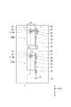
図1は、本発明の第1実施形態に係る半導体レーザ装置1の斜視図である。図1に示すように、本実施形態の半導体レーザ装置1は、ベース10、3個の半導体レーザモジュール20A〜20C、及び集光レンズ40を備えている。半導体レーザ装置1は、半導体レーザモジュール20A〜20Cから出射されたレーザ光を結合させて、光ファイバ50に導光する装置である。なお、説明の便宜上、半導体レーザモジュール20A〜20Cから出射されるレーザ光のファースト取付位置軸方向をX軸方向と、スロー軸方向をY軸方向と、X軸方向及びY軸方向に垂直な方向をZ軸方向とする。また、本明細書では、レーザ光の出射方向を前方といい、その反対方向を後方という。
(First embodiment)
FIG. 1 is a perspective view of a
ベース10は、XZ平面上に配置される板状部材である。ベース10の主面には、半導体レーザモジュール20A〜20C、及び集光レンズ40が載置されている。ベース10は、半導体レーザモジュール20A〜20Cにおいて生じる熱をその下に設けられるヒートシンクに伝熱させ、放熱することで半導体レーザモジュール20A〜20Cを冷却する。
The
半導体レーザモジュール20A〜20Cは、Z軸方向に沿ってベース10上に配列されている。半導体レーザモジュール20A〜20Cは略同一の構成を有しているので、以下では、半導体レーザモジュール20A〜20Cを単に半導体レーザモジュール20と総称してその構成を説明する。
The
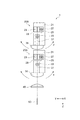
半導体レーザモジュール20は、図2及び図3に示すように、光学ブロック台(光学マウント)21、発光素子23、LDマウント25、ファースト軸コリメータレンズ(以下、「FACレンズ」という。)29、スロー軸コリメータレンズマウント(以下、「SACレンズマウント」という。)31、及びスロー軸コリメータレンズ(以下、「SACレンズ」という。)35を備えている。
2 and 3, the
光学ブロック台21は、直方体形状を呈する、黒アルマイト処理されたアルミニウム製の部材である。光学ブロック台21の一面は、発光素子23を搭載する搭載面とされている。光学ブロック台21の搭載面に垂直な面には、光学ブロック台21をY軸方向に貫通する貫通孔(第1貫通孔)36が設けられている。
The
発光素子23は、活性層を含む積層構造をなす半導体レーザ素子であり、銅製又は銅合金製の直方体形状を有するLDマウント25上に取り付けられている。LDマウント25の発光素子23の出射端面の直近位置には、精密UV硬化樹脂によりFACレンズ29が取り付けられている。FACレンズ29は、発光素子23から出射されたレーザ光をファースト軸方向でコリメートする光学素子である。FACレンズ29は、発光素子23の出射端面から約1m離れた位置に減光フィルタを備えたCCDカメラを配置して、発光素子23から出射されるレーザ光のファースト軸方向のビーム径が最小になり、かつ、平行光が光軸に一致するように調整された状態で、LDマウント25に固定される。
The
LDマウント25は、搭載された発光素子23の出射端面及びFACレンズ29をZ軸方向を向けた状態で、六角スペーサ27により光学ブロック台21の搭載面に固定されている。
The LD mount 25 is fixed to the mounting surface of the
SACレンズ35は、FACレンズ29を通過したレーザ光を、スロー軸方向でコリメートする光学素子である。SACレンズ35は、一例としては焦点距離fが20mmの平凸シリンドリカルレンズである。
The
SACレンズマウント31は、一端部が屈曲部31Bとされた略平板状の部材であり、屈曲部31Bの先端にはSACレンズ35が取り付けられている。平板状部分である平板部31Aの他端部側には、平板部31Aを厚さ方向に貫通する貫通孔(第2貫通孔)31Cが設けられている。
The
光学ブロック台21のLDマウント25取付位置の前方には、搭載面に対して垂直方向に延びるねじ孔(第2ねじ孔)32が形成されており、ねじ33が貫通孔31C及びねじ孔32に挿入されて、SACレンズマウント31と光学ブロック台21とが締結される。ねじ33が緩められた状態では、SACレンズマウント31は、貫通孔31Cを支点として、光学ブロック台21の搭載面に水平な面内で回転可能とされている。一方、ねじ33が締められた状態では、SACレンズマウント31は、光学ブロック台21に固定される。このように、SACレンズマウント31の固定位置を調整することで、レーザ光の光軸に対するSACレンズ35の角度はスロー軸方向で変更可能とされている。貫通孔31C、ねじ孔32、及びねじ33はスロー軸調整機構として機能する。
A screw hole (second screw hole) 32 extending in a direction perpendicular to the mounting surface is formed in front of the mounting position of the
半導体レーザモジュール20は、図4及び図5に示すように、Z軸方向に沿ってベース10上に配列される。なお、図4及び図5では、説明の便宜上、半導体レーザモジュール20A〜20Cのうち、2つの半導体レーザモジュール20A及び20Bのみを図示している。
As shown in FIGS. 4 and 5, the
ベース10には、半導体レーザモジュール20A、20Bの取付位置に対応するように、Z軸方向に延びる一直線の仮想線L上にねじ孔(第1ねじ孔)11が設けられている。ねじ孔11は光学ブロック台21の貫通孔36に対応する取付機構である。
The
半導体レーザモジュール20A、20Bは、搭載面がYZ平面に一致するように、ベース上に搭載され、ねじ37が貫通孔36及びねじ孔11に挿入されることで、半導体レーザモジュール20A、20Bがベース10に締結される。
The
ねじ37が緩められた状態では、半導体レーザモジュール20A、20Bは、貫通孔36を支点としてベース10の水平面内で回転可能とされている。一方、ねじ37が締められた状態では、半導体レーザモジュール20A、20Bは、ベース10に固定される。このように、半導体レーザ装置1では、貫通孔36を支点として半導体レーザモジュール20の向きをX軸方向にあおることができる。これにより、半導体レーザモジュール20から出射されるレーザ光の角度がX軸方向に変更される。貫通孔36、ねじ孔11、及びねじ37はファースト軸調整機構として機能する。
In a state where the
半導体レーザモジュール20Aの光学ブロック台21の幅W1は、半導体レーザモジュール20Aの後段に配置される半導体レーザモジュール20Bの光学ブロック台21の幅W2よりも小さく形成されている。一方、半導体レーザモジュール20Aの光学ブロック台21における搭載面と対向する主面から貫通孔36までの距離と、半導体レーザモジュール20Bの光学ブロック台21における搭載面と対向する主面から貫通孔36までの距離とが同一となるように、貫通孔36が光学ブロック台21にそれぞれ形成されている。このため、半導体レーザモジュール20Aの貫通孔36と半導体レーザモジュール20Aの発光素子23との間隔d1は、半導体レーザモジュール20Bの貫通孔36と半導体レーザモジュール20Bの発光素子23との間隔d2よりも、所定の間隔D(すなわち幅w2と幅w1との差分)だけ短く形成されている。間隔Dは、例えば、1.5mmである。半導体レーザモジュール20A及び半導体レーザモジュール20Bは、それぞれの光学ブロック台21における搭載面と対向する主面が同一平面上に位置するように配置されている。これにより、半導体レーザモジュール20A、20Bから所定の間隔Dだけ離間してレーザ光が出射され、レーザ光が互いに干渉しない。
The width W1 of the
集光レンズ40は、図6及び図7に示すように、半導体レーザモジュール20A〜20Cから互いに平行に出射されたレーザ光を集光させて、それぞれのレーザ光を結合する。結合されたレーザ光は、集光レンズ40の焦点面に配置される光ファイバ50に導光される。集光レンズ40としては、例えばLightpath社製のGRADIUMレンズ(焦点距離f=15mm)を用いることができる。光ファイバ50としては、例えば、Nufern社製のMM−S105/125−15A(コア径:105μmφ、NAO.15)を用いることができる。
As shown in FIGS. 6 and 7, the condensing
次に、半導体レーザモジュール20から出射されるレーザ光の出射角度の調整機構について説明する。上記の通り、ねじ37が緩められた状態では、半導体レーザモジュール20は、貫通孔36を支点としてベース10の水平面内で回転可能とされている。半導体レーザモジュール20は、出力レーザ光の角度がX軸方向で調整されて、最適な結合効率が得られる角度で、ねじ37によりベース10に締結されて、固定される。
Next, a mechanism for adjusting the emission angle of the laser beam emitted from the
また、上記の通り、ねじ33が緩められた状態では、SACレンズマウント31は、貫通孔31Cを支点として、光学ブロック台21の搭載面に水平な面内で回転可能とされ、SACレンズマウント31は、を回転させることで、レーザ光の光軸に対するSACレンズ35の角度はスロー軸方向で変更可能とされている。SACレンズ35は、SACレンズ35の角度がX軸方向で調整されて、最適な結合効率が得られる角度で、ねじ33により光学ブロック台21締結されて、固定される。
Further, as described above, in the state where the
以上説明したように、本実施形態に係る半導体レーザ装置1では、ファースト軸調整機構により半導体レーザモジュール20の向きがベース10に対してファースト軸方向に調整され、スロー軸調整機構によりSACレンズ35が半導体レーザモジュール20に対してスロー軸方向に調整される。これにより、半導体レーザモジュール20の出力レーザ光の出射角度がファースト軸方向及びスロー軸方向に調節される。よって、複数の半導体レーザモジュール20の出力が最適結合状態になるように容易に調芯固定することができ、高い結合効率を実現することができる。
As described above, in the
また、本実施形態に係る半導体レーザ装置1では、集光レンズ40により所定の間隔Dで離間するレーザ光を集光して、結合することができる。
Further, in the
また、本実施形態では、半導体レーザモジュール20を所望の向きにした状態で、11A、11Bとねじ37で半導体レーザモジュール20をベース10に締結することができるので、容易に半導体レーザモジュール20の向きをベース10に対してファースト軸方向に調整することができる。
In the present embodiment, the
また、本実施形態では、ねじ孔11A、11Bは、レーザ光の光軸方向(Z方向)に沿って一直線上に設けられており、半導体レーザモジュール20Aの取付位置と発光素子23との間隔d1が、半導体レーザモジュール20Bの取付位置と発光素子23との間隔d2よりも、所定の間隔Dだけ短く形成されているので、確実に半導体レーザモジュールから所定の間隔Dで離間するレーザ光を出力することができる。
In the present embodiment, the screw holes 11A and 11B are provided on a straight line along the optical axis direction (Z direction) of the laser light, and the distance d1 between the mounting position of the
また、本実施形態では、半導体レーザモジュール20を所望の向きにした状態で、ねじ孔32とねじ33で半導体レーザモジュール20をベース10に締結することができるので、容易にレーザ光に対するSACレンズ35の向きをスロー軸方向に調整することができる。
In the present embodiment, the
(第2実施形態)
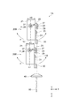
次に、図9を参照して本発明の第2実施形態について説明する。本実施形態に係る半導体レーザ装置1Aは、半導体レーザモジュール20の寸法及び設置位置が第1実施形態と異なり、その他の点は半導体レーザ装置1と同じである。
(Second Embodiment)
Next, a second embodiment of the present invention will be described with reference to FIG. The
半導体レーザ装置1Aでは、ベース10には、Z軸方向に沿った仮想線L1上及び仮想線L2上にねじ孔11が設けられている。仮想線L1及び仮想線L2は所定の間隔Dだけ離間した平行な仮想線である。半導体レーザ装置1Aでは、半導体レーザモジュール20Aの光学ブロック台21の幅W1は、半導体レーザモジュール20Aの後段に配置される半導体レーザモジュール20Bの光学ブロック台21の幅W2よりと同一である。このため、半導体レーザモジュール20Aは、半導体レーザモジュール20Bよりも、所定の間隔DだけX軸方向にずれてベース10に対して取り付けられている。このような構成においても、半導体レーザモジュール20A、20Bから出力されるレーザ光は、所定の間隔Dだけ離間し、互いに干渉しない。
In the
このような半導体レーザ装置1Aにおいても、上述した半導体レーザ装置1と同一の効果を奏する。また、半導体レーザ装置1Aにおいては、半導体レーザモジュール20が同じ形状で形成されているので、製造コストを低減することができる。
Such a
以上、本発明の実施形態について説明したが、本発明は上記実施形態に限られるものではなく、各請求項に記載した要旨を変更しない範囲で変形し、又は他のものに適用したものであってもよい。 As mentioned above, although embodiment of this invention was described, this invention is not limited to the said embodiment, It changed within the range which does not change the summary described in each claim, or was applied to another thing. May be.
例えば、上記実施形態では、半導体レーザ装置1、1Aが半導体レーザモジュール20を3つ備える例を説明したが、本発明に係る半導体レーザ装置は、必要に応じて任意の数の半導体レーザモジュールを備えていてもよい。
For example, in the above embodiment, the example in which the
また、上記実施形態では、光学ブロック21に1つの貫通孔36が設けられており、この貫通孔36を介して半導体レーザモジュール20とベース10とが締結されているが、半導体レーザモジュール20とベース10との締結方法は限定されない。例えば、半導体レーザモジュール20に2つの貫通孔が形成されるとともに、ベース10に半導体レーザモジュール20の貫通孔に対応する2つの貫通孔が形成され、半導体レーザモジュール20の貫通孔及びベース10の貫通孔にボルトが挿入されて、ベースの裏面に配置されたナットにより、半導体レーザモジュール20とベース10とが締結されもよい。この場合には、半導体レーザモジュール20又はベース10に形成される貫通孔の一方をファースト軸方向に延びる長孔とすることで、半導体レーザモジュール20の向きをベースに対してファースト軸方向に調整することができる。
In the above embodiment, one through
以下、実施例に基づいて本実施形態をより具体的に説明するが、本発明はこれらの実施例により何ら限定されるものではない。 Hereinafter, although this embodiment is described more concretely based on an Example, this invention is not limited at all by these Examples.
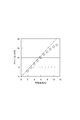
本実施例では、半導体レーザ装置1について結合効率の測定を行った。本実施例では、2つの半導体レーザモジュール20の出力レーザ光を結合した。FACレンズ29としては、Doricレンズ社製のD141−759を用いた。SACレンズとしては、焦点距離fが20mmの平凸シリンドリカルレンズを用いた。集光レンズ40としては、Lightpath社製のGRADIUMレンズ(焦点距離f=15mm)を用いた。光ファイバ50としては、例えば、Nufern社製のMM−S105/125−15A(コア径:105μmφ、NAO.15)を用いた。
In this example, the coupling efficiency of the
上記構成において、半導体レーザ装置1に付与する駆動電流を変化させた場合のファイバ出力の変化を測定した。その結果を図8に示す。図8において、半導体レーザ装置1からのレーザ出力を点線で示す。図8に示すように、本実施例では、コア径105μmφという小さなコア径の光ファイバ50に対して、80%程度の高い結合効率を実現できることが確認された。
In the above configuration, the change in the fiber output when the drive current applied to the
1…半導体レーザ装置、10…ベース、11…ねじ孔、20A,20B,20C…半導体レーザモジュール、21…光学ブロック台、23…発光素子、25…LDマウント、29…FACレンズ、31…SACレンズマウント、31A…平板部、31B…屈曲部、31C…貫通孔、32…ねじ孔、35…SACレンズ、36…貫通孔、40…集光レンズ、50…光ファイバ。
DESCRIPTION OF
Claims (6)
前記ベースの主面上に配置された集光レンズと、
レーザ光を出射する活性層をそれぞれ有する半導体レーザモジュールであって、前記ベースの主面上に、スロー軸が前記ベースの主面と直交し、かつ、前記集光レンズに向けて出射したレーザ光が互いに干渉しないように取り付けられた複数の半導体レーザモジュールと、
前記半導体レーザモジュールの向きを前記ベースに対してファースト軸方向に調整するファースト軸調整機構と、
を備え、
前記半導体レーザモジュールは、
前記活性層を含む発光素子と、
前記発光素子に対して固定され、前記発光素子から出射されたレーザ光を、ファースト軸方向でコリメートするファースト軸コリメータレンズと、
前記ファースト軸コリメータレンズを通過したレーザ光を、スロー軸方向でコリメートするスロー軸コリメータレンズと、
前記スロー軸コリメータレンズの向きを前記半導体レーザモジュールに対してスロー軸方向に調整するスロー軸調整機構と、
を備える半導体レーザ装置。 A base having a main surface;
A condensing lens disposed on the main surface of the base;
Semiconductor laser modules each having an active layer that emits laser light, wherein the laser light emitted on the main surface of the base is perpendicular to the main surface of the base and emitted toward the condenser lens A plurality of semiconductor laser modules mounted so as not to interfere with each other;
A first axis adjustment mechanism for adjusting the direction of the semiconductor laser module in the first axis direction with respect to the base;
With
The semiconductor laser module is:
A light emitting device comprising the active layer;
A first axis collimator lens that is fixed to the light emitting element and collimates the laser light emitted from the light emitting element in the first axis direction;
A slow axis collimator lens that collimates the laser light that has passed through the first axis collimator lens in the slow axis direction;
A slow axis adjustment mechanism for adjusting the direction of the slow axis collimator lens in the slow axis direction with respect to the semiconductor laser module;
A semiconductor laser device comprising:
ファースト軸に直交する面が前記発光素子を搭載する搭載面とされ、かつ、スロー軸方向に第1貫通孔が形成された光学マウントを備え、
前記ファースト軸調整機構は、
前記ベースの主面に対して垂直方向に設けられた第1ねじ孔と、
前記第1貫通孔及び前記第1ねじ孔に挿入される第1ねじと、を備え、
前記第1ねじを前記第1貫通孔及び前記第1ねじ孔に挿入して前記半導体レーザモジュールを前記ベースに取り付ける取付機構である、請求項1又は2に記載の半導体レーザ装置。 The semiconductor laser module is:
A surface orthogonal to the first axis is a mounting surface on which the light emitting element is mounted, and an optical mount in which a first through hole is formed in the slow axis direction,
The first axis adjusting mechanism is
A first screw hole provided in a direction perpendicular to the main surface of the base;
A first screw inserted into the first through hole and the first screw hole,
3. The semiconductor laser device according to claim 1, wherein the semiconductor laser device is an attachment mechanism for attaching the semiconductor laser module to the base by inserting the first screw into the first through hole and the first screw hole.
前記半導体レーザモジュールから出力されるレーザ光の出射方向を前方としたときに、
第1の前記半導体レーザモジュールの前記第1貫通孔と第1の前記半導体レーザモジュールの前記発光素子との間隔は、前記第1の前記半導体レーザモジュールの後段に配置される第2の前記半導体レーザモジュールの前記第1貫通孔と前記第2の前記半導体レーザモジュールの前記発光素子との間隔よりも、所定の間隔だけ短く形成されている、請求項3に記載の半導体レーザ装置。 The first screw hole is provided on a straight line along the optical axis direction of the laser beam,
When the emission direction of the laser beam output from the semiconductor laser module is the front,
The distance between the first through hole of the first semiconductor laser module and the light emitting element of the first semiconductor laser module is the second semiconductor laser disposed at the rear stage of the first semiconductor laser module. 4. The semiconductor laser device according to claim 3, wherein the semiconductor laser device is formed to be shorter by a predetermined interval than an interval between the first through hole of the module and the light emitting element of the second semiconductor laser module.
第1の前記半導体レーザモジュールの前記第1貫通孔と第1の前記半導体レーザモジュールの前記発光素子との間隔は、前記第1の前記半導体レーザモジュールの後段に配置される第2の前記半導体レーザモジュールの前記第1貫通孔と前記第2の前記半導体レーザモジュールの前記発光素子との間隔と、同じ長さで形成されており、
第1の前記半導体レーザモジュールの前記第1貫通孔は、前記第2の前記半導体レーザモジュールの前記第1貫通孔よりも、所定の間隔だけファースト軸方向にずれて前記ベースに取り付けられている、請求項3に記載の半導体レーザ装置。 When the emission direction of the laser beam output from the semiconductor laser module is the front,
The distance between the first through hole of the first semiconductor laser module and the light emitting element of the first semiconductor laser module is the second semiconductor laser disposed at the rear stage of the first semiconductor laser module. The interval between the first through hole of the module and the light emitting element of the second semiconductor laser module is formed with the same length,
The first through hole of the first semiconductor laser module is attached to the base with a predetermined interval shifted from the first through hole of the second semiconductor laser module by a predetermined distance. The semiconductor laser device according to claim 3.
ファースト軸に直交する面が前記発光素子を搭載する搭載面とされ、かつ、前記搭載面に対して垂直に延びる第2ねじ孔が形成された光学マウントと、
前記スロー軸コリメータレンズが固定され、厚さ方向に第2貫通孔が形成されたレンズマウントと、
前記第2貫通孔及び前記第2ねじ孔に挿入される第2ねじと、を備え、
前記第2ねじを前記第2貫通孔及び前記第2ねじ孔に挿入して前記レンズマウントを前記光学マウントに取り付ける取付機構である、請求項1〜5の何れか一項に記載の半導体レーザ装置。 The semiconductor laser module is:
An optical mount in which a surface orthogonal to the first axis is a mounting surface on which the light emitting element is mounted, and a second screw hole extending perpendicularly to the mounting surface is formed;
A lens mount in which the slow axis collimator lens is fixed and a second through hole is formed in the thickness direction;
A second screw inserted into the second through hole and the second screw hole,
6. The semiconductor laser device according to claim 1, wherein the semiconductor laser device is an attachment mechanism that attaches the lens mount to the optical mount by inserting the second screw into the second through hole and the second screw hole. 7. .
Priority Applications (1)
| Application Number | Priority Date | Filing Date | Title |
|---|---|---|---|
| JP2012140885A JP5985899B2 (en) | 2012-06-22 | 2012-06-22 | Semiconductor laser device |
Applications Claiming Priority (1)
| Application Number | Priority Date | Filing Date | Title |
|---|---|---|---|
| JP2012140885A JP5985899B2 (en) | 2012-06-22 | 2012-06-22 | Semiconductor laser device |
Publications (2)
| Publication Number | Publication Date |
|---|---|
| JP2014007232A true JP2014007232A (en) | 2014-01-16 |
| JP5985899B2 JP5985899B2 (en) | 2016-09-06 |
Family
ID=50104721
Family Applications (1)
| Application Number | Title | Priority Date | Filing Date |
|---|---|---|---|
| JP2012140885A Active JP5985899B2 (en) | 2012-06-22 | 2012-06-22 | Semiconductor laser device |
Country Status (1)
| Country | Link |
|---|---|
| JP (1) | JP5985899B2 (en) |
Cited By (3)
| Publication number | Priority date | Publication date | Assignee | Title |
|---|---|---|---|---|
| WO2015145608A1 (en) * | 2014-03-26 | 2015-10-01 | 株式会社島津製作所 | Laser device |
| DE102015105807A1 (en) * | 2015-04-16 | 2016-10-20 | Osram Opto Semiconductors Gmbh | Optoelectronic lighting device |
| JP2017527111A (en) * | 2014-08-14 | 2017-09-14 | エムティティ イノベーション インコーポレイテッドMtt Innovation Incorporated | Multiple laser light sources |
Citations (9)
| Publication number | Priority date | Publication date | Assignee | Title |
|---|---|---|---|---|
| JPH0677608A (en) * | 1992-07-10 | 1994-03-18 | Fujitsu Ltd | Laser diode module |
| JPH08274355A (en) * | 1995-03-31 | 1996-10-18 | Sumitomo Electric Ind Ltd | Two-dimensional array-type optical element module |
| JP2004246158A (en) * | 2003-02-14 | 2004-09-02 | Hamamatsu Photonics Kk | Semiconductor laser system |
| JP2006108501A (en) * | 2004-10-07 | 2006-04-20 | Sony Corp | Laser unit, optical adjusting method thereof, optical apparatus, and its assembling method |
| JP2006216199A (en) * | 2005-02-07 | 2006-08-17 | Sony Corp | Light source and manufacturing method |
| JP2006339569A (en) * | 2005-06-06 | 2006-12-14 | Sony Corp | Laser device and image display apparatus equipped therewith |
| JP2008501144A (en) * | 2004-06-01 | 2008-01-17 | トルンプ フォトニクス,インコーポレイテッド | Optimal matching of the output of a two-dimensional laser array stack to an optical fiber |
| JP2011086905A (en) * | 2009-10-13 | 2011-04-28 | Nalux Co Ltd | Laser assembly |
| JP2011243717A (en) * | 2010-05-18 | 2011-12-01 | Panasonic Corp | Semiconductor laser module and fiber laser using the same |
-
2012
- 2012-06-22 JP JP2012140885A patent/JP5985899B2/en active Active
Patent Citations (9)
| Publication number | Priority date | Publication date | Assignee | Title |
|---|---|---|---|---|
| JPH0677608A (en) * | 1992-07-10 | 1994-03-18 | Fujitsu Ltd | Laser diode module |
| JPH08274355A (en) * | 1995-03-31 | 1996-10-18 | Sumitomo Electric Ind Ltd | Two-dimensional array-type optical element module |
| JP2004246158A (en) * | 2003-02-14 | 2004-09-02 | Hamamatsu Photonics Kk | Semiconductor laser system |
| JP2008501144A (en) * | 2004-06-01 | 2008-01-17 | トルンプ フォトニクス,インコーポレイテッド | Optimal matching of the output of a two-dimensional laser array stack to an optical fiber |
| JP2006108501A (en) * | 2004-10-07 | 2006-04-20 | Sony Corp | Laser unit, optical adjusting method thereof, optical apparatus, and its assembling method |
| JP2006216199A (en) * | 2005-02-07 | 2006-08-17 | Sony Corp | Light source and manufacturing method |
| JP2006339569A (en) * | 2005-06-06 | 2006-12-14 | Sony Corp | Laser device and image display apparatus equipped therewith |
| JP2011086905A (en) * | 2009-10-13 | 2011-04-28 | Nalux Co Ltd | Laser assembly |
| JP2011243717A (en) * | 2010-05-18 | 2011-12-01 | Panasonic Corp | Semiconductor laser module and fiber laser using the same |
Cited By (5)
| Publication number | Priority date | Publication date | Assignee | Title |
|---|---|---|---|---|
| WO2015145608A1 (en) * | 2014-03-26 | 2015-10-01 | 株式会社島津製作所 | Laser device |
| JPWO2015145608A1 (en) * | 2014-03-26 | 2017-04-13 | 株式会社島津製作所 | Laser equipment |
| JP2017527111A (en) * | 2014-08-14 | 2017-09-14 | エムティティ イノベーション インコーポレイテッドMtt Innovation Incorporated | Multiple laser light sources |
| DE102015105807A1 (en) * | 2015-04-16 | 2016-10-20 | Osram Opto Semiconductors Gmbh | Optoelectronic lighting device |
| JP2018516452A (en) * | 2015-04-16 | 2018-06-21 | オスラム オプト セミコンダクターズ ゲゼルシャフト ミット ベシュレンクテル ハフツングOsram Opto Semiconductors GmbH | Optoelectronic lighting equipment |
Also Published As
| Publication number | Publication date |
|---|---|
| JP5985899B2 (en) | 2016-09-06 |
Similar Documents
| Publication | Publication Date | Title |
|---|---|---|
| JP5473535B2 (en) | Light source device | |
| US7515346B2 (en) | High power and high brightness diode-laser array for material processing applications | |
| US9455552B1 (en) | Laser diode apparatus utilizing out of plane combination | |
| KR101623651B1 (en) | Laser light source module and laser light source device | |
| JP5473534B2 (en) | Light source device | |
| US7444047B2 (en) | Multiplexing optical system | |
| JP2004096088A (en) | Multiplex laser light source and aligner | |
| CA2718816C (en) | Laser light source module | |
| JP4742330B2 (en) | Laser assembly | |
| WO2014126124A1 (en) | Semiconductor laser device | |
| JP5985899B2 (en) | Semiconductor laser device | |
| JP6646644B2 (en) | Laser system | |
| US11515689B2 (en) | Semiconductor laser module and method of manufacturing semiconductor laser module | |
| WO2015145608A1 (en) | Laser device | |
| US8646958B2 (en) | Light emitting device | |
| US10746944B2 (en) | Laser device | |
| JP6130427B2 (en) | Laser module | |
| WO2024058273A1 (en) | Vehicle lamp unit | |
| WO2019160038A1 (en) | Semiconductor laser module | |
| JP2022173880A (en) | Ld module, optical device, and heat processing machine | |
| CN115413391A (en) | Light source device, projector, machining device, light source unit, and method for adjusting light source device | |
| JP2019053230A (en) | Optical module and manufacturing method thereof | |
| JP2006108501A (en) | Laser unit, optical adjusting method thereof, optical apparatus, and its assembling method |
Legal Events
| Date | Code | Title | Description |
|---|---|---|---|
| A621 | Written request for application examination |
Free format text: JAPANESE INTERMEDIATE CODE: A621 Effective date: 20150203 |
|
| A977 | Report on retrieval |
Free format text: JAPANESE INTERMEDIATE CODE: A971007 Effective date: 20151130 |
|
| A131 | Notification of reasons for refusal |
Free format text: JAPANESE INTERMEDIATE CODE: A131 Effective date: 20151215 |
|
| A521 | Written amendment |
Free format text: JAPANESE INTERMEDIATE CODE: A523 Effective date: 20160215 |
|
| TRDD | Decision of grant or rejection written | ||
| A01 | Written decision to grant a patent or to grant a registration (utility model) |
Free format text: JAPANESE INTERMEDIATE CODE: A01 Effective date: 20160802 |
|
| A61 | First payment of annual fees (during grant procedure) |
Free format text: JAPANESE INTERMEDIATE CODE: A61 Effective date: 20160804 |
|
| R150 | Certificate of patent or registration of utility model |
Ref document number: 5985899 Country of ref document: JP Free format text: JAPANESE INTERMEDIATE CODE: R150 |