JP2013520002A - Interconnect structure made of redirected carbon nanotubes - Google Patents
Interconnect structure made of redirected carbon nanotubes Download PDFInfo
- Publication number
- JP2013520002A JP2013520002A JP2012552439A JP2012552439A JP2013520002A JP 2013520002 A JP2013520002 A JP 2013520002A JP 2012552439 A JP2012552439 A JP 2012552439A JP 2012552439 A JP2012552439 A JP 2012552439A JP 2013520002 A JP2013520002 A JP 2013520002A
- Authority
- JP
- Japan
- Prior art keywords
- cnt
- along
- bundles
- electronic device
- bundle
- Prior art date
- Legal status (The legal status is an assumption and is not a legal conclusion. Google has not performed a legal analysis and makes no representation as to the accuracy of the status listed.)
- Granted
Links
Images


Classifications
-
- H—ELECTRICITY
- H01—ELECTRIC ELEMENTS
- H01L—SEMICONDUCTOR DEVICES NOT COVERED BY CLASS H10
- H01L21/00—Processes or apparatus adapted for the manufacture or treatment of semiconductor or solid state devices or of parts thereof
- H01L21/70—Manufacture or treatment of devices consisting of a plurality of solid state components formed in or on a common substrate or of parts thereof; Manufacture of integrated circuit devices or of parts thereof
- H01L21/71—Manufacture of specific parts of devices defined in group H01L21/70
- H01L21/768—Applying interconnections to be used for carrying current between separate components within a device comprising conductors and dielectrics
- H01L21/76838—Applying interconnections to be used for carrying current between separate components within a device comprising conductors and dielectrics characterised by the formation and the after-treatment of the conductors
- H01L21/76841—Barrier, adhesion or liner layers
-
- H—ELECTRICITY
- H01—ELECTRIC ELEMENTS
- H01L—SEMICONDUCTOR DEVICES NOT COVERED BY CLASS H10
- H01L23/00—Details of semiconductor or other solid state devices
- H01L23/52—Arrangements for conducting electric current within the device in operation from one component to another, i.e. interconnections, e.g. wires, lead frames
- H01L23/522—Arrangements for conducting electric current within the device in operation from one component to another, i.e. interconnections, e.g. wires, lead frames including external interconnections consisting of a multilayer structure of conductive and insulating layers inseparably formed on the semiconductor body
- H01L23/532—Arrangements for conducting electric current within the device in operation from one component to another, i.e. interconnections, e.g. wires, lead frames including external interconnections consisting of a multilayer structure of conductive and insulating layers inseparably formed on the semiconductor body characterised by the materials
- H01L23/53204—Conductive materials
- H01L23/53276—Conductive materials containing carbon, e.g. fullerenes
-
- H—ELECTRICITY
- H01—ELECTRIC ELEMENTS
- H01L—SEMICONDUCTOR DEVICES NOT COVERED BY CLASS H10
- H01L21/00—Processes or apparatus adapted for the manufacture or treatment of semiconductor or solid state devices or of parts thereof
- H01L21/70—Manufacture or treatment of devices consisting of a plurality of solid state components formed in or on a common substrate or of parts thereof; Manufacture of integrated circuit devices or of parts thereof
- H01L21/71—Manufacture of specific parts of devices defined in group H01L21/70
- H01L21/768—Applying interconnections to be used for carrying current between separate components within a device comprising conductors and dielectrics
- H01L21/76838—Applying interconnections to be used for carrying current between separate components within a device comprising conductors and dielectrics characterised by the formation and the after-treatment of the conductors
- H01L21/76877—Filling of holes, grooves or trenches, e.g. vias, with conductive material
-
- H—ELECTRICITY
- H01—ELECTRIC ELEMENTS
- H01L—SEMICONDUCTOR DEVICES NOT COVERED BY CLASS H10
- H01L24/00—Arrangements for connecting or disconnecting semiconductor or solid-state bodies; Methods or apparatus related thereto
- H01L24/01—Means for bonding being attached to, or being formed on, the surface to be connected, e.g. chip-to-package, die-attach, "first-level" interconnects; Manufacturing methods related thereto
- H01L24/18—High density interconnect [HDI] connectors; Manufacturing methods related thereto
- H01L24/19—Manufacturing methods of high density interconnect preforms
-
- H—ELECTRICITY
- H01—ELECTRIC ELEMENTS
- H01L—SEMICONDUCTOR DEVICES NOT COVERED BY CLASS H10
- H01L24/00—Arrangements for connecting or disconnecting semiconductor or solid-state bodies; Methods or apparatus related thereto
- H01L24/01—Means for bonding being attached to, or being formed on, the surface to be connected, e.g. chip-to-package, die-attach, "first-level" interconnects; Manufacturing methods related thereto
- H01L24/18—High density interconnect [HDI] connectors; Manufacturing methods related thereto
- H01L24/20—Structure, shape, material or disposition of high density interconnect preforms
-
- B—PERFORMING OPERATIONS; TRANSPORTING
- B82—NANOTECHNOLOGY
- B82Y—SPECIFIC USES OR APPLICATIONS OF NANOSTRUCTURES; MEASUREMENT OR ANALYSIS OF NANOSTRUCTURES; MANUFACTURE OR TREATMENT OF NANOSTRUCTURES
- B82Y40/00—Manufacture or treatment of nanostructures
-
- H—ELECTRICITY
- H01—ELECTRIC ELEMENTS
- H01L—SEMICONDUCTOR DEVICES NOT COVERED BY CLASS H10
- H01L2221/00—Processes or apparatus adapted for the manufacture or treatment of semiconductor or solid state devices or of parts thereof covered by H01L21/00
- H01L2221/10—Applying interconnections to be used for carrying current between separate components within a device
- H01L2221/1068—Formation and after-treatment of conductors
- H01L2221/1094—Conducting structures comprising nanotubes or nanowires
-
- H—ELECTRICITY
- H01—ELECTRIC ELEMENTS
- H01L—SEMICONDUCTOR DEVICES NOT COVERED BY CLASS H10
- H01L2224/00—Indexing scheme for arrangements for connecting or disconnecting semiconductor or solid-state bodies and methods related thereto as covered by H01L24/00
- H01L2224/01—Means for bonding being attached to, or being formed on, the surface to be connected, e.g. chip-to-package, die-attach, "first-level" interconnects; Manufacturing methods related thereto
- H01L2224/18—High density interconnect [HDI] connectors; Manufacturing methods related thereto
- H01L2224/20—Structure, shape, material or disposition of high density interconnect preforms
- H01L2224/21—Structure, shape, material or disposition of high density interconnect preforms of an individual HDI interconnect
- H01L2224/215—Material
-
- H—ELECTRICITY
- H01—ELECTRIC ELEMENTS
- H01L—SEMICONDUCTOR DEVICES NOT COVERED BY CLASS H10
- H01L2924/00—Indexing scheme for arrangements or methods for connecting or disconnecting semiconductor or solid-state bodies as covered by H01L24/00
- H01L2924/0001—Technical content checked by a classifier
- H01L2924/0002—Not covered by any one of groups H01L24/00, H01L24/00 and H01L2224/00
-
- Y—GENERAL TAGGING OF NEW TECHNOLOGICAL DEVELOPMENTS; GENERAL TAGGING OF CROSS-SECTIONAL TECHNOLOGIES SPANNING OVER SEVERAL SECTIONS OF THE IPC; TECHNICAL SUBJECTS COVERED BY FORMER USPC CROSS-REFERENCE ART COLLECTIONS [XRACs] AND DIGESTS
- Y10—TECHNICAL SUBJECTS COVERED BY FORMER USPC
- Y10S—TECHNICAL SUBJECTS COVERED BY FORMER USPC CROSS-REFERENCE ART COLLECTIONS [XRACs] AND DIGESTS
- Y10S977/00—Nanotechnology
- Y10S977/84—Manufacture, treatment, or detection of nanostructure
- Y10S977/842—Manufacture, treatment, or detection of nanostructure for carbon nanotubes or fullerenes
-
- Y—GENERAL TAGGING OF NEW TECHNOLOGICAL DEVELOPMENTS; GENERAL TAGGING OF CROSS-SECTIONAL TECHNOLOGIES SPANNING OVER SEVERAL SECTIONS OF THE IPC; TECHNICAL SUBJECTS COVERED BY FORMER USPC CROSS-REFERENCE ART COLLECTIONS [XRACs] AND DIGESTS
- Y10—TECHNICAL SUBJECTS COVERED BY FORMER USPC
- Y10T—TECHNICAL SUBJECTS COVERED BY FORMER US CLASSIFICATION
- Y10T29/00—Metal working
- Y10T29/49—Method of mechanical manufacture
- Y10T29/49002—Electrical device making
- Y10T29/49117—Conductor or circuit manufacturing
Landscapes
- Engineering & Computer Science (AREA)
- Power Engineering (AREA)
- Computer Hardware Design (AREA)
- Microelectronics & Electronic Packaging (AREA)
- General Physics & Mathematics (AREA)
- Condensed Matter Physics & Semiconductors (AREA)
- Physics & Mathematics (AREA)
- Manufacturing & Machinery (AREA)
- Chemical & Material Sciences (AREA)
- Nanotechnology (AREA)
- Crystallography & Structural Chemistry (AREA)
- Internal Circuitry In Semiconductor Integrated Circuit Devices (AREA)
- Carbon And Carbon Compounds (AREA)
Abstract
本発明は、少なくとも2つの異なる方向に沿って伸びる電気接続を含む電子デバイスであって、前記接続は本質的にカーボンナノチューブの束(CNT)(8)を用いて形成され、少なくとも2つのCNT束は、第1方向に沿った軸を有する部分(8a)と、第2方向に沿って方向転換された軸を有する部分(8b)とを含み、前記CNT束間の接続は前記少なくとも2つの束の一部分(8b)の重なりによって達成され、接続ライン(4)を形成する、電子デバイスに関する。 The present invention is an electronic device comprising electrical connections extending along at least two different directions, the connections being formed essentially using a bundle of carbon nanotubes (CNT) (8), wherein at least two CNT bundles Comprises a portion (8a) having an axis along a first direction and a portion (8b) having an axis redirected along a second direction, the connection between the CNT bundles being the at least two bundles To an electronic device, which is achieved by the overlap of a part (8b) of the device and forms a connection line (4).
Description
本開示は、カーボンナノチューブ(CNT)を用いて形成された電気接続部を含む電子デバイスに関する。本開示はまた、このような接続部を形成するための方法に関する。 The present disclosure relates to electronic devices that include electrical connections formed using carbon nanotubes (CNTs). The present disclosure also relates to a method for forming such a connection.
本発明は特に、熱的、電気的、および機械的コネクタに対する用途を有する。 The present invention has particular application to thermal, electrical, and mechanical connectors.
貫通ビアまたはチップ相互接続部を作るためのカーボンナノチューブ(CNT)またはCNT束の使用は、既に提供されており、特に銅の使用に対する補完物またはさらには代替物を提供する。確かに後者は、微小なサイズに関連するときには適していない。CNTはさらに、低い電気抵抗などの必要な特性を有し、異なるチップレベル間の最適な電気伝導率を提供することを可能にする。 The use of carbon nanotubes (CNTs) or CNT bundles to make through vias or chip interconnects has already been provided and provides a complement or even an alternative to the use of copper in particular. Certainly the latter is not suitable when related to small sizes. CNTs further have the necessary properties such as low electrical resistance, making it possible to provide optimal electrical conductivity between different chip levels.
ビアは、導電プレート間の接続を作り出すことができるキャビティである。プレート上に形成された電気ラインは、ビア間の接続を作り出す。導電プレートは、アルミニウムなどの金属で作られ、その中に埋め込まれたビアを形成するキャビティを有する絶縁層によって分けられる。 A via is a cavity that can create a connection between conductive plates. Electrical lines formed on the plate create a connection between vias. The conductive plate is made of a metal such as aluminum and is separated by an insulating layer having a cavity that forms a via embedded therein.
電子デバイスの小型化は、電流密度が高くなりすぎるときに銅がエレクトロマイグレーションによる困難性をもたらすため、銅の使用を非常に厄介にする。銅線およびビアから形成されたアーキテクチャは故に、22ナノメートル付近の解像度(resolution)を有する集積回路において、それらの制限を示す。 The miniaturization of electronic devices makes the use of copper very cumbersome because copper presents electromigration difficulties when the current density becomes too high. The architecture formed from copper lines and vias therefore presents these limitations in integrated circuits with a resolution around 22 nanometers.
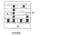
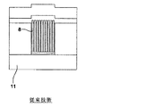
図1および2に示すように、導電性トラック間の接続を確保するためのCNTの使用が、銅またはタングステンビアをCNTで置き換えることによって提供されている(Katagiri et al., Interconnect Technology Conference, 2009. IEEE International 1-3 June 2009, pp. 44- 46;Yokoyama et al. Japanese Journal of Applied Physics, Vol. 47, No 4, 2008, pp. 1985-1990)。しかしながら、この方法は完全に銅を排除することができず、ビア間の接続は銅ラインによって常に確保されている。エレクトロマイグレーションに関する問題は故に、完全に抑えられない。 As shown in FIGS. 1 and 2, the use of CNTs to ensure the connection between conductive tracks is provided by replacing copper or tungsten vias with CNTs (Katagiri et al., Interconnect Technology Conference, 2009). IEEE International 1-3 June 2009, pp. 44-46; Yokoyama et al. Japanese Journal of Applied Physics, Vol. 47, No 4, 2008, pp. 1985-1990). However, this method cannot completely eliminate copper, and the connection between vias is always secured by a copper line. The problems with electromigration are therefore not completely suppressed.
米国特許出願公開第2008/0042287号には、接続が少なくとも部分的にCNT束によって確保されている電子デバイスが記載されている。ビアは、導電材料の層で覆われており、その上には別のCNT束が堆積され、ラインの方向に沿って方向付けされることができる。しかしながら、ビアおよびラインは、同一のCNT束で形成されていない。 US Patent Application Publication No. 2008/0042287 describes an electronic device in which the connection is at least partially secured by a CNT bundle. The via is covered with a layer of conductive material on which another CNT bundle can be deposited and directed along the direction of the line. However, vias and lines are not formed from the same CNT bundle.
米国特許出願公開第2006/0212974号には、ビア内部で準備され、次いで2つの異なるレベルの2つの導電層を接続するための別の方向に沿って方向転換されたCNT束を含む電子デバイスが開示されている。そこには、ビア間の接続がない。 US 2006/0212974 describes an electronic device comprising a CNT bundle prepared inside a via and then redirected along another direction to connect two conductive layers of two different levels. It is disclosed. There are no connections between vias.
中国特許第101562148号は、導電層上にCNT溶液を堆積することによって垂直なCNT接続を作り出すための方法に関する。このデバイスでは、異なるレベルの2つの導電層が、CNT束を用いて接続される。 Chinese Patent No. 101562148 relates to a method for creating a vertical CNT connection by depositing a CNT solution on a conductive layer. In this device, two conductive layers at different levels are connected using a CNT bundle.
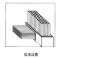
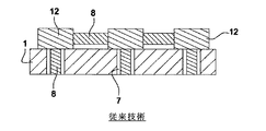
別の技術は、CNTビアと同一の概念をベースとしているが、CNTの方向を変化するために金属ブロックを用いることを含み、故に水平線を形成する(図3)。しかしながら、触媒の堆積および金属ブロックの2つの面における2つの直角に交わる方向に沿ったCNT成長を制御することは難しい(図4)。この技術の別の欠点は、導通を確保するために、多くのCNT−金属界面が繰り返して交差することである。 Another technique is based on the same concept as a CNT via, but involves using a metal block to change the direction of the CNT, thus forming a horizontal line (FIG. 3). However, it is difficult to control catalyst deposition and CNT growth along two perpendicular directions on the two faces of the metal block (FIG. 4). Another drawback of this technique is that many CNT-metal interfaces cross repeatedly to ensure conduction.
米国特許出願公開第2009/0294966号には、2つの導電層間の電気接続を確保する垂直CNTビアだけでなく、ビア間の電気接続を提供する水平CNTラインもまた記載されている。これは、2つの異なる方向に沿って方向付けられた2つの分離した束を含む。ビアに由来するCNT束は、ラインを形成できない。 US Patent Application Publication No. 2009/0294966 describes not only vertical CNT vias that ensure electrical connection between two conductive layers, but also horizontal CNT lines that provide electrical connection between vias. This includes two separate bundles oriented along two different directions. CNT bundles derived from vias cannot form lines.
これらの異なるアプローチは、徐々に小さくなるキャビティ内でのCNT成長の制御、故にCNT束密度の問題の発生を暗示する。確かに、それらの特性およびそれらの方向の均一性と同様に、CNT密度の制御は、ナノエレクトロニクスにおいて良好な電気接続を提供するのに主に重要である。高いCNT密度は、故に必須である。 These different approaches imply the control of CNT growth in the increasingly smaller cavities and hence the occurrence of CNT bundle density problems. Indeed, as well as their properties and the uniformity of their orientation, control of CNT density is primarily important in providing good electrical connections in nanoelectronics. High CNT density is therefore essential.
Hataおよび同僚(Hayamizu et al., Nature nanotechnology, Vol. 3, 2008, 289-294)は近年、散在しているCNTのフィルムをアルコール溶液に浸すことによって得ることができる組織化および緻密化効果を明らかにした。確かに、CNTフィルムがその表面と直角に交わるアルコールバスに浸され、次いで乾燥されるとき、CNTは凝集し整列する。液体の表面張力および強いファンデルワールス相互作用により、CNTはグラファイトに近い構造を達成する。CNTの解離は、緻密化後に観察されない。しかしながら、Hataは同一の方向に沿って方向付けられたCNTで形成された構造を得ただけであり、そのことは故に可能な用途を制限する。 Hata and colleagues (Hayamizu et al., Nature nanotechnology, Vol. 3, 2008, 289-294) have recently demonstrated the organization and densification effects that can be obtained by immersing scattered CNT films in alcoholic solutions. Revealed. Indeed, when the CNT film is immersed in an alcohol bath that intersects the surface at right angles and then dried, the CNTs aggregate and align. Due to the surface tension of the liquid and strong van der Waals interactions, CNTs achieve a structure close to that of graphite. CNT dissociation is not observed after densification. However, Hata has only obtained structures formed with CNTs oriented along the same direction, which therefore limits the possible applications.
本発明は特に、金属の使用を排除することができ、単純な製造プロセスで実施できる技術的解決策に対する探索に由来する。 The present invention derives in particular from the search for technical solutions that can eliminate the use of metals and can be implemented with a simple manufacturing process.
従って本発明は、金属の使用を排除でき、プレート間の接続を確保するか、またはCNT束の方向の変化を確保する、カーボンナノチューブ(CNT)の成長および方向転換(redirection)に基づく新規なアーキテクチャを提供する。 Thus, the present invention is a novel architecture based on the growth and redirection of carbon nanotubes (CNTs) that can eliminate the use of metals and ensure connections between plates or ensure a change in the direction of CNT bundles. I will provide a.
一般的に、本発明は、第1方向に沿って方向付けられ、ビアと呼ばれるキャビティに含まれるカーボンナノチューブ(CNT)の束とともに、電子デバイスに電気接続を形成する段階を含む。このようなCNT束は、同様に第2方向に沿ったCNT束で形成されたラインによって横方向に相互接続される。 In general, the present invention includes the step of forming an electrical connection to an electronic device with a bundle of carbon nanotubes (CNTs) oriented along a first direction and contained in a cavity called a via. Such CNT bundles are interconnected laterally by lines formed by CNT bundles along the second direction as well.
詳細な説明の残りの部分では、“ビア”および“ライン”との用語はそれぞれ、キャビティまたはビアに含まれるCNT束および代表的な接続ラインを指定するために使用される。 In the remainder of the detailed description, the terms “via” and “line” are used to designate the CNT bundle and representative connection lines contained in the cavity or via, respectively.
典型的に、本発明による電子デバイスは、絶縁体層(シリカまたは低誘電率(low-K)マイクロエレクトロニクス材料)で覆われた(例えば、アルミニウムから成る)導電プレートから特に成る一連の構造を含む。ラインによって相互接続されたキャビティは、絶縁ブロックに埋め込まれ、プレート(ビア)間またはビア(ライン)間の相互接続を作り出す。 Typically, an electronic device according to the present invention comprises a series of structures consisting in particular of a conductive plate (eg made of aluminum) covered with an insulator layer (silica or a low-k microelectronic material). . The cavities interconnected by the lines are embedded in the insulating block and create interconnections between plates (vias) or vias (lines).
より具体的には、本発明は、少なくとも2つの異なる方向に沿って伸びる電気接続を含む電子デバイスに関する。典型的に、前記接続は本質的に、カーボンナノチューブ(CNT)の束を用いて形成され、少なくとも2つのCNT束は、第1方向に沿って方向付けられた軸を有する部分と、第2方向に沿って方向転換された軸を有する部分とを含む。さらに、CNT束間の接続は、前記少なくとも2つのCNT束の一部が重なることによって達成され、接続ラインを形成する。 More specifically, the present invention relates to electronic devices that include electrical connections that extend along at least two different directions. Typically, the connection is essentially formed using a bundle of carbon nanotubes (CNTs), where at least two CNT bundles have a portion having an axis oriented along a first direction and a second direction. And a portion having an axis redirected along. Further, the connection between the CNT bundles is achieved by overlapping a part of the at least two CNT bundles to form a connection line.
電気接続を形成する少なくとも2つの束は曲がっており、CNT束の一領域は第1方向に沿っていて、別の領域は第2の異なる方向に沿っている。 At least two bundles forming the electrical connection are bent, one region of the CNT bundle is along the first direction and the other region is along the second different direction.
本発明の電気接続システムは、少なくとも2つの方向、有利に垂直および水平方向における接続を形成することができるが、具体的に水平面における2つの異なる接続の場合には、2つを超える方向、特に3方向において接続を作り出すためにも使用され得ることに、留意すべきである。 The electrical connection system of the present invention can form connections in at least two directions, preferably in the vertical and horizontal directions, but in particular in the case of two different connections in the horizontal plane, more than two directions, in particular Note that it can also be used to create connections in three directions.
本発明によると、電気接続は主に、CNT束または房(bunches)を用いて形成され、つまり、大量の凝集されたカーボンナノチューブは、実質的に平行な成長軸を有する。“本質的に(essentially)”との用語は、電気接続がただCNTによって確保され得るだけであり、故に、金属ラインまたはブロック以外は依然として従来技術のケースである、ということを示す。しかしながら、以下に記載するように、束間の電気接触は、さらに金属の堆積を実施することによって改善され得る。 According to the present invention, the electrical connection is mainly formed using CNT bundles or bunches, i.e. large quantities of agglomerated carbon nanotubes have substantially parallel growth axes. The term “essentially” indicates that the electrical connection can only be secured by the CNTs, and therefore other than metal lines or blocks are still the case of the prior art. However, as described below, the electrical contact between the bundles can be improved by performing further metal deposition.
実際に、このような電気接続は、以下の方法:
−第1方向に沿って少なくとも1つのCNT束を成長させる段階
−有利には液体を流すことによって、第2方向に沿ってCNT束の一部分を方向転換する段階
を実施することによって作り出される。
In fact, such an electrical connection is the following way:
-Growing at least one CNT bundle along the first direction-Produced by performing a step of redirecting a portion of the CNT bundle along the second direction, preferably by flowing a liquid.
典型的に、本発明による電子デバイス内で、少なくとも2つの方向における電気接続を作り出す方法は、
−前記デバイスのキャビティで、第1方向に沿って少なくとも2つのCNT束を成長させる段階
−有利には液体を流すことによって、第2方向に沿って前記2つのCNT束の一部分を方向転換し、接続ラインを形成する段階
を含む。
Typically, a method for creating an electrical connection in at least two directions within an electronic device according to the invention comprises:
-Growing at least two CNT bundles along a first direction in the cavity of the device-redirecting a portion of the two CNT bundles along a second direction, preferably by flowing a liquid; Forming a connection line.
このデバイスの形成段階は故に、従来技術で試されテストされた技術によって、特に鉄などの触媒を用いて、キャビティ内で第1方向に沿ってCNT束を制御して成長させる段階を含む。 The formation stage of this device thus involves the controlled growth of CNT bundles along the first direction in the cavity by means of techniques tested and tested in the prior art, in particular using a catalyst such as iron.
典型的に、CNT束の成長は、前記束がビアよりも少なくとも大きい高さを有するときに停止される。これらのCNT束の一部分は次いで、有利には液体を流すことによって、第2方向に沿って方向転換される。 Typically, CNT bundle growth is stopped when the bundle has a height that is at least greater than the via. A portion of these CNT bundles is then redirected along the second direction, preferably by flowing a liquid.
CNT束の方向転換は、Hayamizuらの文献(Nature nanotechnology, Vol. 3, 2008, 289-294)に記載された技術によって実施され得る。実際に、それは、イソプロピルアルコール溶液にCNTを浸す段階と、グルーブの方向と平行にそれらを引き出す段階とを含み、前記グルーブは液体のメニスカスと直角に交わる。この操作はまた、CNT束の密度を高くすることができる。 The redirection of the CNT bundle can be performed by the technique described in Hayamizu et al. (Nature nanotechnology, Vol. 3, 2008, 289-294). In practice, it involves immersing CNTs in an isopropyl alcohol solution and pulling them parallel to the direction of the grooves, said grooves intersecting the liquid meniscus at right angles. This operation can also increase the density of the CNT bundle.
特権を有する実施形態によると、第2方向に沿って方向転換されたCNT束の一部分は、第1方向に沿ったCNT束の一部分と実質的に直角に交わる。 According to a privileged embodiment, the portion of the CNT bundle redirected along the second direction intersects substantially perpendicular to the portion of the CNT bundle along the first direction.
典型的に、第1方向は実質的に垂直である。有利に、第1方向に沿ったCNT束の一部分は、電子デバイスのビアを形成する。 Typically, the first direction is substantially vertical. Advantageously, a portion of the CNT bundle along the first direction forms a via of the electronic device.
優先的に、第2方向は実質的に水平である。有利に、第2方向に沿ったCNT束の一部分は、電子デバイスの接続ラインを形成する。 Preferentially, the second direction is substantially horizontal. Advantageously, a part of the CNT bundle along the second direction forms a connection line of the electronic device.
特権を有する実施形態では、ビアおよびラインは故に、実質的に直角に交わる。 In privileged embodiments, the vias and lines therefore intersect substantially at right angles.
ビア間の接続を形成するために、具体的に、本発明による電子デバイスは優先的に、第2方向に沿ってそれらの一部分を有する少なくとも2つのCNT束を含み、それは実質的に水平であり得、接続ラインを形成する。そのラインは有利に、第2方向に沿ったCNT束の一部分が重なることによって、つまり、束の端の連続的な重ね合わせによって形成される。 Specifically, to form a connection between vias, an electronic device according to the present invention preferentially includes at least two CNT bundles having portions thereof along a second direction, which are substantially horizontal And connecting lines are formed. The line is advantageously formed by overlapping portions of the CNT bundle along the second direction, i.e. by continuous superposition of the ends of the bundle.
この実施形態は、以下の方法:
−有利にはビア内で、第1方向に沿った複数の平行なCNT束を成長させる段階
−第2方向に沿ってCNT束の一部分を方向転換させる段階
−有利には重なることによって、第2方向に沿ったCNT束の一部分を接続し、接続ラインを形成する段階
によって実施される。
This embodiment comprises the following method:
-Growing a plurality of parallel CNT bundles along a first direction, preferably in a via-turning a part of the CNT bundles along a second direction-advantageously by overlapping the second This is performed by connecting a part of the CNT bundle along the direction to form a connection line.
重なりは実際には、CNT束の上の部分を平らにすることによって、故に、好ましくは実質的に垂直である第1方向において、キャビティに含まれるCNT束の一部分のみをそのままにすることによって得られる。有利には、第2方向、つまり重なりの方向は、接続ラインを含むために事前に絶縁ブロックに埋め込まれたグルーブの方向である。 The overlap is actually obtained by flattening the upper part of the CNT bundle, and thus leaving only a part of the CNT bundle contained in the cavity in the first direction, which is preferably substantially vertical. It is done. Advantageously, the second direction, i.e. the direction of overlap, is the direction of the grooves previously embedded in the insulating block to include the connecting lines.
特定の実施形態によると、本発明のデバイスはさらに、金属層を含む。有利に、それは第2方向に沿った少なくともCNT束の一部分を覆い、より有利には依然として接続ラインである。 According to certain embodiments, the device of the present invention further comprises a metal layer. Advantageously, it covers at least a part of the CNT bundle along the second direction, more advantageously still a connection line.
この金属層は、
−カプセル化のためのデバイスの表面の均一化、または上部接続レベルを形成するための支持体としての使用を可能にし得る。後者の場合、有利には例えばアルミニウムなどの金属材料を堆積することができ、第2のCNTレベルの成長を促進することができる。
−ビア間の接続の促進を可能にし得る。
This metal layer
-It may be possible to make the surface of the device uniform for encapsulation or use as a support to form the upper connection level. In the latter case, a metal material such as, for example, aluminum can be advantageously deposited, which can promote the growth of the second CNT level.
-It may be possible to facilitate the connection between vias.
この金属層は、当業者に既知の任意の適合された技術を用いて堆積される。 This metal layer is deposited using any suitable technique known to those skilled in the art.
別の実施形態によると、電子デバイスはさらに、第2方向におけるその一部分のレベルで、デバイスの少なくとも1つのCNT束と横方向に接続された別のCNT束を含むことができ、ラインを形成する。この他のCNT束は、ビアに由来する束との接続、場合によっては幾つかのビア間の接続を確保する。接続は、前に記載したように、第2方向に沿って直接、または第2方向に沿ったその方向転換の後の何れかにおいて、この他のCNT束の成長後に達成される。 According to another embodiment, the electronic device can further include another CNT bundle laterally connected to at least one CNT bundle of the device at a level of its portion in the second direction, forming a line. . Other CNT bundles ensure connections with bundles derived from vias and, in some cases, connections between several vias. The connection is achieved after the growth of this other CNT bundle, either as described previously, either directly along the second direction or after its turn along the second direction.
優先的に、他のCNT束は、少なくとも2つのCNT束と横方向で接続され、ビア間の接続を確保する。 Preferentially, the other CNT bundles are connected laterally with at least two CNT bundles to ensure a connection between vias.
選択された操作モードによると、ビアまたは接続ラインの何れかを形成するCNT束の成長は、同時にまたは別々に起こり得る。 Depending on the mode of operation selected, the growth of CNT bundles forming either vias or connecting lines can occur simultaneously or separately.
有利に、他のCNT束の成長は、キャビティ内ではなくグルーブ内で実施される。他のCNT束は故に、導電プレートと直接接触することができないが、それは、それが絶縁ブロックによってそれから物理的に分離されているからである。第2方向に沿ったこの他のCNT束の方向転換は、グルーブで実施され得る。 Advantageously, the growth of other CNT bundles is performed in the groove rather than in the cavity. Other CNT bundles can therefore not be in direct contact with the conductive plate because it is physically separated from it by an insulating block. This redirection of other CNT bundles along the second direction can be performed in the groove.
この特定の実施形態では、CNT束間の横方向の接続は有利に、金属層の堆積によって達成される。実際に、それは2つのタイプのCNT束の界面に位置する:第2方向の沿ったその一部分のレベルにおける少なくとも1つのCNT束はビアに由来し、他の束はラインを形成する。この層は有利に、以下の群から選択されるいわゆる接触金属を用いて形成される:パラジウム、銅、金、またはチタン。故に、接触金属は、ビアに由来するCNT束と接続ラインを形成するCNT束との間の接続を確保する。 In this particular embodiment, the lateral connection between the CNT bundles is advantageously achieved by deposition of a metal layer. In fact, it is located at the interface of the two types of CNT bundles: at least one CNT bundle at the level of that portion along the second direction originates from the via and the other bundle forms a line. This layer is advantageously formed using a so-called contact metal selected from the following group: palladium, copper, gold or titanium. Therefore, the contact metal ensures the connection between the CNT bundle originating from the via and the CNT bundle forming the connection line.
本発明との関連で、所定の成長領域にCNTを位置するために、
−プレート全体に成長触媒を堆積し、次いでそれを(エッチング、研磨などによって)規定されていない領域から除去するか、または
−Dijonらの文献(Diam. Relat. Mater., 2009, doi:10.1016/j.diamond.2009.11.017)に記載されているように、規定されていない領域にTiNを堆積し、次いでウエハ全体に触媒を堆積するか
の何れかを実施し得る。
In the context of the present invention, in order to locate CNTs in a predetermined growth region,
-Deposit the growth catalyst over the entire plate and then remove it from undefined areas (by etching, polishing, etc.) or-Dijon et al. (Diam. Relat. Mater., 2009, doi: 10.1016 / j.diamond.2009.11.017), either TiN can be deposited in undefined areas and then the catalyst can be deposited over the entire wafer.
好ましい実施形態によると、本発明による電子デバイス内で少なくとも2つの方向において電気接続を作り出す方法は、第2方向に沿ったCNT束の一部分上に少なくとも1つの金属層を堆積する段階をさらに含む。 According to a preferred embodiment, the method for creating an electrical connection in at least two directions within an electronic device according to the invention further comprises depositing at least one metal layer on a portion of the CNT bundle along the second direction.
それはまた、第2方向に沿った一部分のレベルにおいて、少なくとも1つのCNT束の横方向の接続を目的とする別のCNT束を成長させ、場合によっては第2方向に沿って方向転換させ、接続ラインを形成する段階を含むことができる。この特定のケースでは、その方法は場合によっては、他のCNT束上での金属層の堆積段階を含むことができる。 It also grows, at some level along the second direction, another CNT bundle intended for lateral connection of at least one CNT bundle, possibly turning and connecting along the second direction. A step of forming a line can be included. In this particular case, the method may optionally include a metal layer deposition step on other CNT bundles.
さらに、本発明によるデバイスを形成する方法は、CNTが成長すべきでない領域にTiNを堆積する少なくとも1つの段階を含むことができる。 Furthermore, the method of forming a device according to the present invention can include at least one step of depositing TiN in areas where CNTs are not to be grown.
本発明による電子デバイスでは、電流はカーボンナノチューブを介して本質的に流れるように見え、故にエレクトロマイグレーション問題を大幅に減少させる。さらに、このようなデバイスを形成する方法は、比較的試されテストされた技術で実行される。 In the electronic device according to the invention, the current appears to flow essentially through the carbon nanotubes, thus greatly reducing electromigration problems. Furthermore, the method of forming such devices is performed with relatively tried and tested techniques.
発明の前述のおよび他の特徴および利点は、添付の図面と関連する以下の実施形態の以下の非限定的な説明に記載される。 The foregoing and other features and advantages of the invention are set forth in the following non-limiting description of the following embodiments in conjunction with the accompanying drawings.
以下に記載される異なる実施形態は、垂直および水平相互接続の両方を必要とする、故に2つの異なる直角に交わる方向における電子デバイスに関する。これらの接続は全て、カーボンナノチューブ(CNT)を用いて形成される:
−垂直接続は、絶縁材料層で形成されるビア内に成長する垂直CNT束によって形成され;
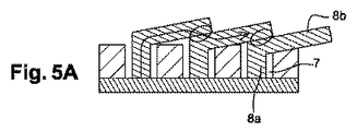
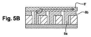
−水平接続はまた、CNTによって確保され、接続ラインを形成する。それらは、ビアに由来する束の重なりによって生じることがあり、前記束は方向転換されているか(第1実施形態;図5A)、またはビアに由来する束と横方向に接触する独立の束の成長によって生じ、前記束は方向転換されている(第2実施形態;図5B)。
The different embodiments described below relate to electronic devices that require both vertical and horizontal interconnections, and thus in two different perpendicular directions. All these connections are made using carbon nanotubes (CNT):
The vertical connection is formed by a vertical CNT bundle growing in a via formed of an insulating material layer;
-Horizontal connections are also secured by CNTs to form connection lines. They may be caused by the overlap of bundles derived from vias, said bundles being redirected (first embodiment; FIG. 5A) or of independent bundles that are in lateral contact with the bundles derived from vias. Due to the growth, the bundle is redirected (second embodiment; FIG. 5B).
特定の実施形態によると、金属層2、10はまた、特にCNT束の部分8b(図6Aおよび図6B)においてCNT束と接触する。
According to a particular embodiment, the
このような層は有利に、
−例えばPdまたはTiで作られ、故にCNTの接触を改善する層10;および/または
−例えばAlで作られ、新規のCNTレベル、故に新規の相互接続レベルの成長を可能にする層2;
から形成され得る。
Such a layer is advantageously
A
Can be formed from
代わりにそれは、2つのタイプの層10および2に関連する二層であり得る。
Instead, it can be a bilayer associated with two types of
[I/本発明の第1実施形態]
既に述べたように、垂直CNT束の重なりによるこの第1実施形態が、図5Aおよび6Aにそれぞれ示される。
[I / First embodiment of the present invention]
As already mentioned, this first embodiment with overlapping vertical CNT bundles is shown in FIGS. 5A and 6A, respectively.
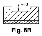
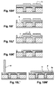
より具体的には、その形成方法が図8に示される。段階AからFは、概略的に端面図で、つまりグルーブ3と直角に交わって示され、図8Gおよび8Hは、グルーブ3の方向に水平な図面に対応することに、留意すべきである。
More specifically, the formation method is shown in FIG. It should be noted that stages A to F are shown schematically in an end view, i.e. at right angles to groove 3, and FIGS. 8G and 8H correspond to drawings horizontal to the direction of
<A/ベース構造の形成>
シリカまたはマイクロエレクトロニクスの低誘電率(low-K)材料で作られる絶縁層1が、導電層2に堆積される。導体2は典型的には、アルミニウムである。
<A/Formation of base structure>
An insulating
<B/グルーブのエッチング>
絶縁体1内に、将来のライン4となるグルーブ3が、従来のリソグラフィ方法によって形成される。
<B / groove etching>
A
<C/TiN堆積>
略50ナノメートルの厚さを有するTiN層5が、可能ならば等角堆積方法を用いて、グルーブ3に堆積される。TiNは、ここでは鉄である触媒6がTiNに堆積されるとき、カーボンナノチューブの成長を抑制する作用を有する。
<C / TiN deposition>
A
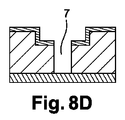
<D/ビアの開口>
ビア7がグルーブ3内に開口され、絶縁体1を通り抜けるエッチングは導体2で止まる。
<D / via opening>
A via 7 is opened in the
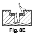
<E/触媒の堆積>
触媒6の堆積は、常温で実施される。それは典型的に、1ナノメートルの鉄の層であり、蒸発またはイオンビームスパッタリングによって堆積される。堆積は、側面の被覆を最小化するために、垂直入射で実施される。
<E / Catalyst deposition>
The
<F/選択的なナノチューブの成長>
従来的には、カーボンナノチューブ(CNT)8は、室温で形成されたRF空気プラズマを用いて鉄を前もって酸化した後、600°Cで、C2H2+H2+He混合物(10sccm、50sccm、50sccm)を用いて成長される。プラズマ条件は以下の通りである:
−P=0.3Torr;
−30分間わたり、70−W power
<F / Selective nanotube growth>
Traditionally, carbon nanotubes (CNTs) 8 are pre-oxidized with RF air plasma formed at room temperature, then at 600 ° C, C 2 H 2 + H 2 + He mixture (10 sccm, 50 sccm , 50 sccm). The plasma conditions are as follows:
−P = 0.3 Torr;
70-W power for 30 minutes
本方法は、鉄がTiN5上に堆積される場合を除き、鉄6上でのナノチューブ8の成長を可能にする。この場合には、成長はない。
The method allows the growth of
600℃での成長の間の圧力は、1Torrである。反応性ガスは、コールドプラズマ後に導入され、温度の上昇は、15分以内に、0.3-Torrの圧力で実施される。 The pressure during growth at 600 ° C. is 1 Torr. The reactive gas is introduced after the cold plasma and the temperature increase is carried out at a pressure of 0.3-Torr within 15 minutes.
ナノチューブ8の高さは、成長時間で規定される。
The height of the
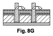
<G/ナノチューブの方向転換>
成長の後、デバイスはイソプロピルアルコールに浸され、グルーブ3の方向と直角に交わる方向に引き出される:液体のメニスカスは、グルーブ3に垂直である。グルーブのチューブを通って流れる液体は、ビア7に由来するチューブ8を平らにする。チューブは、この操作後に高く緻密化される。さらに、チューブ8は、2つの異なる部分:
−ビア7と平行な軸を有する部分8a、および
−グルーブ3と平行な軸を有する部分8b
を有する。
<G / Nanotube direction change>
After growth, the device is immersed in isopropyl alcohol and pulled out in a direction perpendicular to the direction of groove 3: the liquid meniscus is perpendicular to groove 3. The liquid flowing through the groove tube flattens the
A
Have
異なるビア7に由来するナノチューブ束8は、こうしてグルーブ3内で平らにされ、接触し始める。異なるビア7に由来する少なくとも2つのナノチューブ束の重なりによって、こうしてライン接続4を形成することができる。
Nanotube bundles 8 originating from
この段階の終わりに、図5Aに示すような相互接続システムが得られる。ライン4は、ビア7に由来するナノチューブ束8bの重なりによって形成される。この実施形態では、ライン抵抗Rは、ナノチューブ抵抗に加えられた一連の界面抵抗で形成される。
At the end of this phase, an interconnect system as shown in FIG. 5A is obtained. Line 4 is formed by the overlap of
しかしながら、後続の段階(図8H)において、構造を平坦化し、次のレベル(カプセル化)でその操作(相互接続の創作)を繰り返すことが出来るように、ライン4の表面で、再びアルミニウムで金属の堆積2を実施することが推奨され得る。この段階の終わりに、図6Aに示すような相互接続システムが得られる。 However, in a subsequent stage (FIG. 8H), the surface of line 4 is again metalized with aluminum so that the structure can be flattened and the operation (creation of interconnections) can be repeated at the next level (encapsulation). It may be recommended to perform a second deposition. At the end of this stage, an interconnection system as shown in FIG. 6A is obtained.
[II/本発明の第2実施形態]
この第2実施形態は、図5B、6B、7、9および10に示される。
[II / Second Embodiment of the Invention]
This second embodiment is shown in FIGS. 5B, 6B, 7, 9 and 10.
図5Bは、1つの界面抵抗しか残っていないため、ライン抵抗が第1実施形態よりも低いという事実を示す。 FIG. 5B shows the fact that the line resistance is lower than in the first embodiment because only one interface resistance remains.
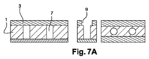
図7は、実質的に直角に交わる相互接続部、それぞれビア7およびライン4が、有利には同時に形成された少なくとも2つの異なるナノチューブ束に由来する、この第2実施形態の原理を示す図面である。左側の図面が断面図を示し、右側の図面が上面図を示すことに、留意すべきである。 FIG. 7 is a drawing showing the principle of this second embodiment, in which the interconnects intersecting substantially at right angles, respectively vias 7 and lines 4, are preferably derived from at least two different nanotube bundles formed simultaneously. is there. It should be noted that the left drawing shows a cross-sectional view and the right drawing shows a top view.
さらに、ライン4およびビア7からナノチューブ8および8’が同時に成長することを暗示する実施形態が図9に示され、それは図8に由来する。
Furthermore, an embodiment is shown in FIG. 9, which implies that
段階AからCは、図8のそれと同様である。 Steps A to C are the same as those in FIG.
しかしながら、ビア7の開口の前に、追加の段階が実施される(図9D’):TiN5の開口9がグルーブ3に形成され、触媒6の堆積後に、この領域でカーボンナノチューブ8’の成長が得られる。これは、ラインの成長領域9のアレンジに対応する。
However, an additional step is performed before the opening of via 7 (FIG. 9D ′): TiN5 opening 9 is formed in
次の段階は、樹脂層で開口9を保護した後に、ビア7を開口する段階を含む(図9E’)。
The next step includes the step of opening the via 7 after protecting the
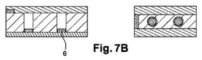
触媒6の堆積後(図9F’)および成長段階の間(図9G’)、チューブ8および8’がそれぞれ、ビア7で成長し、成長領域9においてラインレベルで形成される。CNT8および8’に由来する束は、触媒の厚さを変えることで、かつビアおよびラインでのプラズマ条件を変えることで、異なる長さで提供され得る。
After deposition of catalyst 6 (FIG. 9F ′) and during the growth phase (FIG. 9G ′),
ビア7および成長領域9のそれぞれに由来する2つのナノチューブ束(8,8’)の方向転換の後、得られた相互接続システムは、図5Bに示されるものに対応する。ビア7に由来しないナノチューブ束8’を用いて接続ライン4が形成されることが観察できる。
After turning of the two nanotube bundles (8,8 ') originating from each of the via 7 and the
図10は図8に由来するが、その実施形態では、ナノチューブ8および8’の成長はライン4およびビア7から別々に実施され、界面金属10が(それぞれ、ビア8bのCNTとライン8’のCNTとの間の)2つのナノチューブ束の間に挿入される。
FIG. 10 is derived from FIG. 8, but in that embodiment, the growth of
その方法は、図8の段階A〜Gで始まる。 The method begins with steps AG in FIG.
しかしながら、段階Hの代わりに、図10の段階H’からM’が実施される。 However, instead of stage H, stages H 'to M' of FIG.
<H’/接触金属の堆積>
ビア7に由来するナノチューブ8(8a、8b)の方向転換の後、パラジウム、銅、金、またはチタンなどの接触金属10が堆積される。
<H '/ deposition of contact metal>
After turning of the nanotubes 8 (8a, 8b) originating from the
<I’/接触金属の開口>
接触金属10は次いで、グルーブ3の終端から絶縁体1まで、エッチングによって開口される。ライン4に由来する将来のナノチューブ8’の成長領域 9 は、こうして形成される。
<I '/ Contact metal opening>
The
<J’/触媒の堆積>
触媒は、蒸発またはスパッタリングによって堆積される。
<J '/ Catalyst deposition>
The catalyst is deposited by evaporation or sputtering.
<K’/接触金属の平坦化>
デバイスは、触媒6を成長領域9に保持しながら、接触金属10上への触媒の堆積6を抑えるために、CMP(“化学機械研磨(Chemical and Mechanical Polishing)”)によって平坦化される。
<K '/ flattening of contact metal>
The device is planarized by CMP (“Chemical and Mechanical Polishing”) to suppress
<L’/第2ナノチューブの成長>
図8の段階Fと同じ条件での第2の成長が実施される。成長領域9に由来し、ライン4を形成することを目的とするナノチューブ束8’は、こうして得られる。
<L '/ Growth of second nanotube>
A second growth is performed under the same conditions as in Step F of FIG. A
<M’/ラインの方向転換>
成長の後、ナノチューブ束は、図8の段階Gと同じ方法で方向転換される。ビア7に由来するナノチューブ8を有するコンタクトビア金属10における接続ライン4は、こうして得られる。
<M '/ Change of line direction>
After growth, the nanotube bundle is redirected in the same way as in stage G of FIG. The connection line 4 in the contact via
このようなプロセスの終わりに、図6Bに示すような相互接続システムが得られる。 At the end of such a process, an interconnect system as shown in FIG. 6B is obtained.
1 絶縁層
2、10 金属層
3 グルーブ
5 TiN
6 触媒
7 ビア
8、8a、8b、8’ ナノチューブ
9 開口
1 Insulating
6
Claims (13)
−有利には液体を流すことによって、第2方向に沿って前記2つのCNT束の一部分(8b)を方向転換し、前記接続ライン(4)を形成する段階と、
を含む、請求項1から7の何れか1項に記載の電子デバイス内で、少なくとも2つの方向における電気接続を作り出す方法。 -Growing at least two CNT bundles (8) along a first direction in the cavity of the device;
-Turning a portion (8b) of the two CNT bundles along a second direction, preferably by flowing a liquid, to form the connecting line (4);
A method of creating electrical connections in at least two directions within an electronic device according to any one of the preceding claims.
−前記CNT束の一部分(8b)が前記第2方向に沿って方向転換され、
−前記第2方向に沿ったCNT束の一部分(8b)が重なりによって接続され、前記接続ライン(4)を形成する
ことを特徴とする、請求項8に記載の方法。 The growth of a plurality of parallel CNT bundles (8) along said first direction is advantageously carried out in the vias;
-A portion (8b) of the CNT bundle is redirected along the second direction;
Method according to claim 8, characterized in that a part (8b) of the CNT bundles along the second direction are connected by overlapping to form the connection line (4).
Applications Claiming Priority (3)
| Application Number | Priority Date | Filing Date | Title |
|---|---|---|---|
| FR1050986A FR2956243B1 (en) | 2010-02-11 | 2010-02-11 | INTERCONNECTION STRUCTURE BASED ON REDIRECTED CARBON NANOTUBES |
| FR1050986 | 2010-02-11 | ||
| PCT/FR2010/052792 WO2011098679A1 (en) | 2010-02-11 | 2010-12-17 | Interconnection structure made of redirected carbon nanotubes |
Publications (2)
| Publication Number | Publication Date |
|---|---|
| JP2013520002A true JP2013520002A (en) | 2013-05-30 |
| JP5699164B2 JP5699164B2 (en) | 2015-04-08 |
Family
ID=42667917
Family Applications (1)
| Application Number | Title | Priority Date | Filing Date |
|---|---|---|---|
| JP2012552439A Expired - Fee Related JP5699164B2 (en) | 2010-02-11 | 2010-12-17 | Interconnect structure made of redirected carbon nanotubes |
Country Status (8)
| Country | Link |
|---|---|
| US (2) | US20120292103A1 (en) |
| EP (1) | EP2534678B1 (en) |
| JP (1) | JP5699164B2 (en) |
| KR (1) | KR101721060B1 (en) |
| CN (1) | CN102725839A (en) |
| ES (1) | ES2531431T3 (en) |
| FR (1) | FR2956243B1 (en) |
| WO (1) | WO2011098679A1 (en) |
Families Citing this family (5)
| Publication number | Priority date | Publication date | Assignee | Title |
|---|---|---|---|---|
| US9096784B2 (en) | 2010-07-23 | 2015-08-04 | International Business Machines Corporation | Method and system for allignment of graphite nanofibers for enhanced thermal interface material performance |
| US9257359B2 (en) * | 2011-07-22 | 2016-02-09 | International Business Machines Corporation | System and method to process horizontally aligned graphite nanofibers in a thermal interface material used in 3D chip stacks |
| US9245813B2 (en) | 2013-01-30 | 2016-01-26 | International Business Machines Corporation | Horizontally aligned graphite nanofibers in etched silicon wafer troughs for enhanced thermal performance |
| US9090004B2 (en) | 2013-02-06 | 2015-07-28 | International Business Machines Corporation | Composites comprised of aligned carbon fibers in chain-aligned polymer binder |
| US9082744B2 (en) | 2013-07-08 | 2015-07-14 | International Business Machines Corporation | Method for aligning carbon nanotubes containing magnetic nanoparticles in a thermosetting polymer using a magnetic field |
Citations (7)
| Publication number | Priority date | Publication date | Assignee | Title |
|---|---|---|---|---|
| JP2002329723A (en) * | 2001-05-02 | 2002-11-15 | Fujitsu Ltd | Integrated circuit device and its manufacturing method |
| JP2006228818A (en) * | 2005-02-15 | 2006-08-31 | Fujitsu Ltd | Method of forming carbon nanotube, and method of manufacturing electronic device |
| JP2006255867A (en) * | 2005-03-18 | 2006-09-28 | Fujitsu Ltd | Carbon nanotube device and manufacturing method thereof |
| US20080042287A1 (en) * | 2004-07-29 | 2008-02-21 | International Business Machines Corporation | Integrated Circuit Chip Utilizing Oriented Carbon Nanotube Conductive Layers |
| JP2008044099A (en) * | 2006-08-11 | 2008-02-28 | Kofukin Seimitsu Kogyo (Shenzhen) Yugenkoshi | Carbon nanotube composite material and manufacturing method thereof |
| JP2009032819A (en) * | 2007-07-25 | 2009-02-12 | Fujitsu Ltd | Manufacturing method of electronic-device, and electronic device using the method |
| JP2010006696A (en) * | 2008-06-27 | 2010-01-14 | Commissariat A L'energie Atomique | Method for producing carbon nanotube mat on conductor or semiconductor material |
Family Cites Families (3)
| Publication number | Priority date | Publication date | Assignee | Title |
|---|---|---|---|---|
| US20100244262A1 (en) * | 2003-06-30 | 2010-09-30 | Fujitsu Limited | Deposition method and a deposition apparatus of fine particles, a forming method and a forming apparatus of carbon nanotubes, and a semiconductor device and a manufacturing method of the same |
| US20090294966A1 (en) * | 2008-05-27 | 2009-12-03 | Unidym, Inc. | Carbon nanotubes as interconnects in integrated circuits and method of fabrication |
| CN101562148B (en) * | 2009-04-24 | 2011-08-24 | 北京大学 | Method for carbon nano tube to achieve vertical interconnection of upper and lower layers of conductive material |
-
2010
- 2010-02-11 FR FR1050986A patent/FR2956243B1/en not_active Expired - Fee Related
- 2010-12-17 CN CN2010800626547A patent/CN102725839A/en active Pending
- 2010-12-17 ES ES10807619.1T patent/ES2531431T3/en active Active
- 2010-12-17 JP JP2012552439A patent/JP5699164B2/en not_active Expired - Fee Related
- 2010-12-17 EP EP10807619.1A patent/EP2534678B1/en not_active Not-in-force
- 2010-12-17 KR KR1020127020149A patent/KR101721060B1/en active IP Right Grant
- 2010-12-17 US US13/575,371 patent/US20120292103A1/en not_active Abandoned
- 2010-12-17 WO PCT/FR2010/052792 patent/WO2011098679A1/en active Application Filing
-
2014
- 2014-06-27 US US14/317,708 patent/US9165825B2/en not_active Expired - Fee Related
Patent Citations (7)
| Publication number | Priority date | Publication date | Assignee | Title |
|---|---|---|---|---|
| JP2002329723A (en) * | 2001-05-02 | 2002-11-15 | Fujitsu Ltd | Integrated circuit device and its manufacturing method |
| US20080042287A1 (en) * | 2004-07-29 | 2008-02-21 | International Business Machines Corporation | Integrated Circuit Chip Utilizing Oriented Carbon Nanotube Conductive Layers |
| JP2006228818A (en) * | 2005-02-15 | 2006-08-31 | Fujitsu Ltd | Method of forming carbon nanotube, and method of manufacturing electronic device |
| JP2006255867A (en) * | 2005-03-18 | 2006-09-28 | Fujitsu Ltd | Carbon nanotube device and manufacturing method thereof |
| JP2008044099A (en) * | 2006-08-11 | 2008-02-28 | Kofukin Seimitsu Kogyo (Shenzhen) Yugenkoshi | Carbon nanotube composite material and manufacturing method thereof |
| JP2009032819A (en) * | 2007-07-25 | 2009-02-12 | Fujitsu Ltd | Manufacturing method of electronic-device, and electronic device using the method |
| JP2010006696A (en) * | 2008-06-27 | 2010-01-14 | Commissariat A L'energie Atomique | Method for producing carbon nanotube mat on conductor or semiconductor material |
Also Published As
| Publication number | Publication date |
|---|---|
| EP2534678A1 (en) | 2012-12-19 |
| US9165825B2 (en) | 2015-10-20 |
| EP2534678B1 (en) | 2015-02-11 |
| WO2011098679A1 (en) | 2011-08-18 |
| JP5699164B2 (en) | 2015-04-08 |
| KR101721060B1 (en) | 2017-04-10 |
| US20140338189A1 (en) | 2014-11-20 |
| FR2956243A1 (en) | 2011-08-12 |
| CN102725839A (en) | 2012-10-10 |
| FR2956243B1 (en) | 2013-10-25 |
| US20120292103A1 (en) | 2012-11-22 |
| KR20120113766A (en) | 2012-10-15 |
| ES2531431T3 (en) | 2015-03-16 |
Similar Documents
| Publication | Publication Date | Title |
|---|---|---|
| US7960277B2 (en) | Electronic device and method of manufacturing the same | |
| JP5699164B2 (en) | Interconnect structure made of redirected carbon nanotubes | |
| TWI564241B (en) | Beol interconnect with carbon nanotubes | |
| US8338822B2 (en) | Electrical connection structure having elongated carbon structures with fine catalyst particle layer | |
| TW200931531A (en) | Method for forming cu wiring | |
| JP2009027157A (en) | Method for manufacturing carbon nanotube-based electrical connection | |
| US8533945B2 (en) | Wiring structure and method of forming the same | |
| JP2012049268A (en) | Method for manufacturing semiconductor substrate | |
| CN102881651B (en) | A kind of method improving electrical interconnection characteristic of carbon nano tube | |
| JP2013535820A (en) | Method and structure for improving the conductivity of narrow copper filled vias | |
| JP2008258184A (en) | Electronic device and its manufacturing method | |
| Kawabata et al. | Robustness of CNT via interconnect fabricated by low temperature process over a high-density current | |
| TWI428274B (en) | Process of nanotubes with internal connections | |
| Katagiri et al. | Carbon nanotube vias fabricated by remote plasma-enhanced chemical vapor deposition | |
| US20060138668A1 (en) | Passivation structure for semiconductor devices | |
| KR100713916B1 (en) | Method of manufacturing semiconductor device | |
| JP2010263227A (en) | Method for manufacturing electrical connection structure | |
| CN106356329B (en) | The forming method of the dielectric capping layers of copper-connection | |
| KR20230108327A (en) | CMOS compatible graphene structures, interconnects and fabrication methods | |
| JP2004031497A (en) | Semiconductor device and its manufacturing method | |
| Xu et al. | Through-wafer interconnects using carbon nanotubes synthesized by chemical vapor deposition |
Legal Events
| Date | Code | Title | Description |
|---|---|---|---|
| A621 | Written request for application examination |
Free format text: JAPANESE INTERMEDIATE CODE: A621 Effective date: 20131025 |
|
| A977 | Report on retrieval |
Free format text: JAPANESE INTERMEDIATE CODE: A971007 Effective date: 20140618 |
|
| A131 | Notification of reasons for refusal |
Free format text: JAPANESE INTERMEDIATE CODE: A131 Effective date: 20140707 |
|
| A601 | Written request for extension of time |
Free format text: JAPANESE INTERMEDIATE CODE: A601 Effective date: 20140925 |
|
| A602 | Written permission of extension of time |
Free format text: JAPANESE INTERMEDIATE CODE: A602 Effective date: 20141002 |
|
| A601 | Written request for extension of time |
Free format text: JAPANESE INTERMEDIATE CODE: A601 Effective date: 20141208 |
|
| A521 | Request for written amendment filed |
Free format text: JAPANESE INTERMEDIATE CODE: A523 Effective date: 20141215 |
|
| A602 | Written permission of extension of time |
Free format text: JAPANESE INTERMEDIATE CODE: A602 Effective date: 20141215 |
|
| TRDD | Decision of grant or rejection written | ||
| A01 | Written decision to grant a patent or to grant a registration (utility model) |
Free format text: JAPANESE INTERMEDIATE CODE: A01 Effective date: 20150119 |
|
| A61 | First payment of annual fees (during grant procedure) |
Free format text: JAPANESE INTERMEDIATE CODE: A61 Effective date: 20150216 |
|
| R150 | Certificate of patent or registration of utility model |
Ref document number: 5699164 Country of ref document: JP Free format text: JAPANESE INTERMEDIATE CODE: R150 |
|
| LAPS | Cancellation because of no payment of annual fees |