JP2013247672A - Window structure, method of manufacturing the same, electronic device equipped with camera, and method of manufacturing the same - Google Patents
Window structure, method of manufacturing the same, electronic device equipped with camera, and method of manufacturing the same Download PDFInfo
- Publication number
- JP2013247672A JP2013247672A JP2013010361A JP2013010361A JP2013247672A JP 2013247672 A JP2013247672 A JP 2013247672A JP 2013010361 A JP2013010361 A JP 2013010361A JP 2013010361 A JP2013010361 A JP 2013010361A JP 2013247672 A JP2013247672 A JP 2013247672A
- Authority
- JP
- Japan
- Prior art keywords
- window
- hole
- layer
- design
- design layer
- Prior art date
- Legal status (The legal status is an assumption and is not a legal conclusion. Google has not performed a legal analysis and makes no representation as to the accuracy of the status listed.)
- Granted
Links
- 238000004519 manufacturing process Methods 0.000 title claims abstract description 41
- 230000031700 light absorption Effects 0.000 claims abstract description 89
- 239000000758 substrate Substances 0.000 claims description 32
- 238000000034 method Methods 0.000 claims description 18
- 229920002799 BoPET Polymers 0.000 claims description 8
- 238000007650 screen-printing Methods 0.000 claims description 7
- 239000004973 liquid crystal related substance Substances 0.000 claims description 5
- 239000000853 adhesive Substances 0.000 description 7
- 230000001070 adhesive effect Effects 0.000 description 7
- 238000007639 printing Methods 0.000 description 6
- 239000011521 glass Substances 0.000 description 3
- NIXOWILDQLNWCW-UHFFFAOYSA-N acrylic acid group Chemical group C(C=C)(=O)O NIXOWILDQLNWCW-UHFFFAOYSA-N 0.000 description 2
- 230000000052 comparative effect Effects 0.000 description 2
- 230000001788 irregular Effects 0.000 description 2
- 239000000463 material Substances 0.000 description 2
- 238000012986 modification Methods 0.000 description 2
- 230000004048 modification Effects 0.000 description 2
- 229920000139 polyethylene terephthalate Polymers 0.000 description 2
- 239000005020 polyethylene terephthalate Substances 0.000 description 2
- 229920005989 resin Polymers 0.000 description 2
- 239000011347 resin Substances 0.000 description 2
- 238000000926 separation method Methods 0.000 description 2
- 229920003002 synthetic resin Polymers 0.000 description 2
- 239000000057 synthetic resin Substances 0.000 description 2
- -1 Polyethylene Terephthalate Polymers 0.000 description 1
- 208000006930 Pseudomyxoma Peritonei Diseases 0.000 description 1
- 238000001035 drying Methods 0.000 description 1
- 230000014509 gene expression Effects 0.000 description 1
- 229910052751 metal Inorganic materials 0.000 description 1
- 239000002184 metal Substances 0.000 description 1
- 230000002093 peripheral effect Effects 0.000 description 1
- 239000004033 plastic Substances 0.000 description 1
- 229920003023 plastic Polymers 0.000 description 1
- 229920000306 polymethylpentene Polymers 0.000 description 1
- 239000000843 powder Substances 0.000 description 1
- 238000003825 pressing Methods 0.000 description 1
- 229910052709 silver Inorganic materials 0.000 description 1
- 239000004332 silver Substances 0.000 description 1
- 239000012780 transparent material Substances 0.000 description 1
Images


Classifications
-
- G—PHYSICS
- G03—PHOTOGRAPHY; CINEMATOGRAPHY; ANALOGOUS TECHNIQUES USING WAVES OTHER THAN OPTICAL WAVES; ELECTROGRAPHY; HOLOGRAPHY
- G03B—APPARATUS OR ARRANGEMENTS FOR TAKING PHOTOGRAPHS OR FOR PROJECTING OR VIEWING THEM; APPARATUS OR ARRANGEMENTS EMPLOYING ANALOGOUS TECHNIQUES USING WAVES OTHER THAN OPTICAL WAVES; ACCESSORIES THEREFOR
- G03B11/00—Filters or other obturators specially adapted for photographic purposes
-
- H—ELECTRICITY
- H01—ELECTRIC ELEMENTS
- H01L—SEMICONDUCTOR DEVICES NOT COVERED BY CLASS H10
- H01L31/00—Semiconductor devices sensitive to infrared radiation, light, electromagnetic radiation of shorter wavelength or corpuscular radiation and specially adapted either for the conversion of the energy of such radiation into electrical energy or for the control of electrical energy by such radiation; Processes or apparatus specially adapted for the manufacture or treatment thereof or of parts thereof; Details thereof
- H01L31/02—Details
- H01L31/0216—Coatings
- H01L31/02161—Coatings for devices characterised by at least one potential jump barrier or surface barrier
- H01L31/02162—Coatings for devices characterised by at least one potential jump barrier or surface barrier for filtering or shielding light, e.g. multicolour filters for photodetectors
- H01L31/02165—Coatings for devices characterised by at least one potential jump barrier or surface barrier for filtering or shielding light, e.g. multicolour filters for photodetectors using interference filters, e.g. multilayer dielectric filters
-
- G—PHYSICS
- G02—OPTICS
- G02B—OPTICAL ELEMENTS, SYSTEMS OR APPARATUS
- G02B27/00—Optical systems or apparatus not provided for by any of the groups G02B1/00 - G02B26/00, G02B30/00
- G02B27/0018—Optical systems or apparatus not provided for by any of the groups G02B1/00 - G02B26/00, G02B30/00 with means for preventing ghost images
-
- G—PHYSICS
- G02—OPTICS
- G02B—OPTICAL ELEMENTS, SYSTEMS OR APPARATUS
- G02B5/00—Optical elements other than lenses
- G02B5/003—Light absorbing elements
-
- G—PHYSICS
- G02—OPTICS
- G02B—OPTICAL ELEMENTS, SYSTEMS OR APPARATUS
- G02B5/00—Optical elements other than lenses
- G02B5/005—Diaphragms
-
- G—PHYSICS
- G02—OPTICS
- G02B—OPTICAL ELEMENTS, SYSTEMS OR APPARATUS
- G02B5/00—Optical elements other than lenses
- G02B5/20—Filters
- G02B5/22—Absorbing filters
-
- G—PHYSICS
- G03—PHOTOGRAPHY; CINEMATOGRAPHY; ANALOGOUS TECHNIQUES USING WAVES OTHER THAN OPTICAL WAVES; ELECTROGRAPHY; HOLOGRAPHY
- G03B—APPARATUS OR ARRANGEMENTS FOR TAKING PHOTOGRAPHS OR FOR PROJECTING OR VIEWING THEM; APPARATUS OR ARRANGEMENTS EMPLOYING ANALOGOUS TECHNIQUES USING WAVES OTHER THAN OPTICAL WAVES; ACCESSORIES THEREFOR
- G03B11/00—Filters or other obturators specially adapted for photographic purposes
- G03B11/04—Hoods or caps for eliminating unwanted light from lenses, viewfinders or focusing aids
-
- G—PHYSICS
- G03—PHOTOGRAPHY; CINEMATOGRAPHY; ANALOGOUS TECHNIQUES USING WAVES OTHER THAN OPTICAL WAVES; ELECTROGRAPHY; HOLOGRAPHY
- G03B—APPARATUS OR ARRANGEMENTS FOR TAKING PHOTOGRAPHS OR FOR PROJECTING OR VIEWING THEM; APPARATUS OR ARRANGEMENTS EMPLOYING ANALOGOUS TECHNIQUES USING WAVES OTHER THAN OPTICAL WAVES; ACCESSORIES THEREFOR
- G03B17/00—Details of cameras or camera bodies; Accessories therefor
- G03B17/02—Bodies
-
- H—ELECTRICITY
- H01—ELECTRIC ELEMENTS
- H01L—SEMICONDUCTOR DEVICES NOT COVERED BY CLASS H10
- H01L31/00—Semiconductor devices sensitive to infrared radiation, light, electromagnetic radiation of shorter wavelength or corpuscular radiation and specially adapted either for the conversion of the energy of such radiation into electrical energy or for the control of electrical energy by such radiation; Processes or apparatus specially adapted for the manufacture or treatment thereof or of parts thereof; Details thereof
- H01L31/02—Details
- H01L31/0216—Coatings
- H01L31/02161—Coatings for devices characterised by at least one potential jump barrier or surface barrier
- H01L31/02162—Coatings for devices characterised by at least one potential jump barrier or surface barrier for filtering or shielding light, e.g. multicolour filters for photodetectors
- H01L31/02164—Coatings for devices characterised by at least one potential jump barrier or surface barrier for filtering or shielding light, e.g. multicolour filters for photodetectors for shielding light, e.g. light blocking layers, cold shields for infrared detectors
-
- H—ELECTRICITY
- H01—ELECTRIC ELEMENTS
- H01L—SEMICONDUCTOR DEVICES NOT COVERED BY CLASS H10
- H01L31/00—Semiconductor devices sensitive to infrared radiation, light, electromagnetic radiation of shorter wavelength or corpuscular radiation and specially adapted either for the conversion of the energy of such radiation into electrical energy or for the control of electrical energy by such radiation; Processes or apparatus specially adapted for the manufacture or treatment thereof or of parts thereof; Details thereof
- H01L31/02—Details
- H01L31/0232—Optical elements or arrangements associated with the device
-
- H—ELECTRICITY
- H01—ELECTRIC ELEMENTS
- H01L—SEMICONDUCTOR DEVICES NOT COVERED BY CLASS H10
- H01L31/00—Semiconductor devices sensitive to infrared radiation, light, electromagnetic radiation of shorter wavelength or corpuscular radiation and specially adapted either for the conversion of the energy of such radiation into electrical energy or for the control of electrical energy by such radiation; Processes or apparatus specially adapted for the manufacture or treatment thereof or of parts thereof; Details thereof
- H01L31/18—Processes or apparatus specially adapted for the manufacture or treatment of these devices or of parts thereof
-
- H—ELECTRICITY
- H10—SEMICONDUCTOR DEVICES; ELECTRIC SOLID-STATE DEVICES NOT OTHERWISE PROVIDED FOR
- H10K—ORGANIC ELECTRIC SOLID-STATE DEVICES
- H10K59/00—Integrated devices, or assemblies of multiple devices, comprising at least one organic light-emitting element covered by group H10K50/00
- H10K59/60—OLEDs integrated with inorganic light-sensitive elements, e.g. with inorganic solar cells or inorganic photodiodes
Landscapes
- Physics & Mathematics (AREA)
- General Physics & Mathematics (AREA)
- Optics & Photonics (AREA)
- Engineering & Computer Science (AREA)
- Power Engineering (AREA)
- Electromagnetism (AREA)
- Computer Hardware Design (AREA)
- Microelectronics & Electronic Packaging (AREA)
- Condensed Matter Physics & Semiconductors (AREA)
- Manufacturing & Machinery (AREA)
- Life Sciences & Earth Sciences (AREA)
- Chemical & Material Sciences (AREA)
- Inorganic Chemistry (AREA)
- Sustainable Development (AREA)
- Optical Elements Other Than Lenses (AREA)
- Studio Devices (AREA)
Abstract
Description
本発明は、ウィンドウ構造物、その製造方法、カメラが搭載された電子装置、及びその製造方法に関する。 The present invention relates to a window structure, a manufacturing method thereof, an electronic device equipped with a camera, and a manufacturing method thereof.
携帯電話、PMPなどの電子機器に使われる各種表示パネル上にはウィンドウが配置され、前記ウィンドウには各種ロゴやアイコンが印刷されるデザイン層を付着することができる。一方、最近では、各種電子機器にカメラが搭載される傾向があり、カメラセンサーに入射する光の経路としてのホールが前記デザイン層に形成されることがある。 Windows are arranged on various display panels used in electronic devices such as mobile phones and PMPs, and a design layer on which various logos and icons are printed can be attached to the windows. On the other hand, recently, there is a tendency that cameras are mounted on various electronic devices, and a hole as a path of light incident on the camera sensor may be formed in the design layer.
しかし、前記デザイン層が有彩色または白色の場合、前記ホールを通過する光が前記ホールに隣接する前記デザイン層の部分で乱反射を起こすことがあり、これによって、撮影物周辺に前記デザイン層の色(色相)が伝達される現象、即ち、一種のビネッティング(vignetting)現象が発生する。 However, when the design layer is chromatic or white, the light passing through the hole may cause irregular reflection in the portion of the design layer adjacent to the hole. A phenomenon in which (hue) is transmitted, that is, a kind of vignetting phenomenon occurs.
本発明の一目的は、ビネッティング現象を防止できるウィンドウ構造物を提供することにある。 An object of the present invention is to provide a window structure capable of preventing the vignetting phenomenon.
本発明の他の目的は、ビネッティング現象を防止できるウィンドウ構造物を製造する方法を提供することにある。 Another object of the present invention is to provide a method of manufacturing a window structure that can prevent vignetting.
本発明のさらに他の目的は、ビネッティング現象を防止できるウィンドウ構造物を含むカメラが搭載された電子装置を提供することにある。 Still another object of the present invention is to provide an electronic device equipped with a camera including a window structure that can prevent a vignetting phenomenon.
本発明のさらに他の目的は、ビネッティング現象を防止できるウィンドウ構造物を含むカメラが搭載された電子装置を製造する方法を提供することにある。 It is still another object of the present invention to provide a method of manufacturing an electronic device equipped with a camera including a window structure that can prevent a vignetting phenomenon.
本発明が解決しようとする課題は、上述した課題に限定されるのではなく、本発明の思想及び領域から逸脱しない範囲内で多様に拡張することができる。 The problems to be solved by the present invention are not limited to the problems described above, but can be variously expanded without departing from the spirit and scope of the present invention.
上述した本発明の一目的を達成するために、本発明の一側面に係るウィンドウ構造物は、ウィンドウ、前記ウィンドウ上に形成され、当該ウィンドウの一部を露出させる第1ホールを有するデザイン層構造物、前記デザイン層構造物上に形成され、前記第1ホールに連通する第2ホールを有する光遮蔽層、並びに前記第1及び第2ホールによって露出される前記デザイン層構造物の部分を少なくとも覆い、前記ウィンドウの一部を露出させる第3ホールを有する光吸収層を含む。 In order to achieve the above-described object of the present invention, a window structure according to one aspect of the present invention is a design layer structure having a window, a first hole formed on the window and exposing a part of the window. A light shielding layer formed on the design layer structure and having a second hole communicating with the first hole, and at least a portion of the design layer structure exposed by the first and second holes. And a light absorption layer having a third hole exposing a part of the window.
上記ウィンドウ構造物において、前記第2ホールは、前記第1ホールよりも大きな直径を有することができる。 In the window structure, the second hole may have a larger diameter than the first hole.
上記ウィンドウ構造物において、前記第1及び第2ホールは、同じ大きさの直径を有することができる。 In the window structure, the first and second holes may have the same diameter.
上記ウィンドウ構造物において、前記光吸収層は、前記第2ホールによって露出する前記光遮蔽層の側壁の少なくとも一部を覆うことができる。 In the window structure, the light absorption layer may cover at least a part of a side wall of the light shielding layer exposed by the second hole.
上記ウィンドウ構造物において、前記光吸収層は、前記光遮蔽層の上面の一部を覆うことができる。 In the window structure, the light absorption layer may cover a part of the upper surface of the light shielding layer.
上記ウィンドウ構造物において、前記光吸収層は、前記光遮蔽層の上面には形成されないことができる。 In the window structure, the light absorption layer may not be formed on an upper surface of the light shielding layer.
上記ウィンドウ構造物において、前記デザイン層構造物は、前記ウィンドウ上に積層された複数のデザイン層を含むことができる。 In the window structure, the design layer structure may include a plurality of design layers stacked on the window.
上記ウィンドウ構造物において、前記第1ホールは、前記ウィンドウから遠ざかるほど直径が大きくなる階段形状を有することができる。 In the window structure, the first hole may have a stepped shape having a diameter that increases as the distance from the window increases.
上記ウィンドウ構造物において、前記第1ホールは、前記ウィンドウの表面に対して垂直な方向に一定の直径を有することができる。 In the window structure, the first hole may have a certain diameter in a direction perpendicular to a surface of the window.
上記ウィンドウ構造物において、前記デザイン層構造物は、有彩色または白色であることができ、前記光遮蔽層及び前記光吸収層は、黒色または灰色であることができる。 In the window structure, the design layer structure may be chromatic or white, and the light shielding layer and the light absorption layer may be black or gray.
上記ウィンドウ構造物において、前記デザイン層構造物、前記光遮蔽層、及び前記光吸収層の各々は、印刷層であることができる。 In the window structure, each of the design layer structure, the light shielding layer, and the light absorption layer may be a printing layer.
上記ウィンドウ構造物において、前記第1〜第3ホールは、上面から見たとき、円形であることができ、前記光吸収層は、上面から見たとき、円形、楕円形、または多角形の外形を有することができる。 In the window structure, the first to third holes may have a circular shape when viewed from above, and the light absorption layer has a circular, elliptical, or polygonal shape when viewed from above. Can have.
上記ウィンドウ構造物において、前記第3ホールは、前記ウィンドウの表面に対して垂直な側壁を有することができる。 In the window structure, the third hole may have a side wall perpendicular to a surface of the window.
上記ウィンドウ構造物において、前記第3ホールは、前記ウィンドウの表面に対して傾斜した側壁を有することができる。 In the window structure, the third hole may have a sidewall inclined with respect to a surface of the window.
上記ウィンドウ構造物において、前記第3ホールの側壁は、曲線形状を有することができる。 In the window structure, the sidewall of the third hole may have a curved shape.
上記ウィンドウ構造物は、前記ウィンドウ上に形成されたPET(Polyethylene Terephthalate)フィルムをさらに含むことができ、前記デザイン層構造物は、前記PETフィルム上に形成されることができる。 The window structure may further include a PET (Polyethylene Terephthalate) film formed on the window, and the design layer structure may be formed on the PET film.
上記ウィンドウ構造物において、前記第3ホールは、前記光吸収層の上方に配置されるカメラセンサーに入斜する光の経路としての役割を果たすことができる。 In the window structure, the third hole may serve as a path of light entering the camera sensor disposed above the light absorption layer.
上述した本発明の他の目的を達成するために、本発明の他の側面に係るウィンドウ構造物の製造方法は、ウィンドウ上に当該ウィンドウの一部を露出させる第1ホールを有するデザイン層構造物を形成し、前記デザイン層構造物上に前記第1ホールに連通する第2ホールを有する光遮蔽層を形成し、前記第1及び第2ホールによって露出する前記デザイン層構造物の部分を少なくとも覆い、前記ウィンドウの一部を露出させる第3ホールを有する光吸収層を形成する。 In order to achieve another object of the present invention described above, a method for manufacturing a window structure according to another aspect of the present invention includes a design layer structure having a first hole exposing a part of the window on the window. A light shielding layer having a second hole communicating with the first hole is formed on the design layer structure, and at least a portion of the design layer structure exposed by the first and second holes is covered. Then, a light absorption layer having a third hole exposing a part of the window is formed.
上記製造方法において、前記光遮蔽層を形成する時、前記第2ホールが前記第1ホールよりも大きな直径を有するように、前記光遮蔽層を形成することができる。 In the manufacturing method, when the light shielding layer is formed, the light shielding layer can be formed such that the second hole has a larger diameter than the first hole.
上記製造方法において、前記光吸収層を形成する時、前記第2ホールによって露出する前記光遮蔽層の側壁の少なくとも一部を覆うように、前記光吸収層を形成することができる。 In the manufacturing method, when the light absorption layer is formed, the light absorption layer can be formed so as to cover at least a part of the side wall of the light shielding layer exposed by the second hole.
上記製造方法において、前記光吸収層を形成する時、前記光遮蔽層の上面の一部を覆うように、前記光吸収層を形成することができる。 In the said manufacturing method, when forming the said light absorption layer, the said light absorption layer can be formed so that a part of upper surface of the said light shielding layer may be covered.
上記製造方法において、前記デザイン層構造物を形成する時、前記ウィンドウ上に複数のデザイン層を積層することができる。 In the manufacturing method, when the design layer structure is formed, a plurality of design layers can be stacked on the window.
上記製造方法において、前記デザイン層構造物を形成する時、前記複数のデザイン層によって生成される前記第1ホールが前記ウィンドウから遠ざかるほど直径が大きくなる階段形状を有するように、前記デザイン層構造物を形成することができる。 In the manufacturing method, when the design layer structure is formed, the design layer structure has a step shape in which the diameter of the first hole generated by the plurality of design layers increases as the distance from the window increases. Can be formed.
上記製造方法において、前記デザイン層構造物、前記光遮蔽層、及び前記光吸収層は、印刷工程を通じて形成することができる。 In the manufacturing method, the design layer structure, the light shielding layer, and the light absorption layer can be formed through a printing process.
上述した本発明のさらに他の目的を達成するために、本発明のさらに他の側面に係るウィンドウ構造物は、ウィンドウ、前記ウィンドウ上に形成され、当該ウィンドウの一部を露出させる第1ホールを有するデザイン層構造物、及び前記ウィンドウ上に形成され、前記デザイン層構造物を覆いつつ、前記ウィンドウの一部を露出させる第2ホールを有する光遮蔽層を含む。 In order to achieve another object of the present invention described above, a window structure according to still another aspect of the present invention includes a window, a first hole formed on the window and exposing a part of the window. And a light shielding layer having a second hole formed on the window and covering the design layer structure and exposing a part of the window.
上記ウィンドウ構造物において、前記デザイン層構造物は、前記ウィンドウ上に積層された複数のデザイン層を含むことができる。 In the window structure, the design layer structure may include a plurality of design layers stacked on the window.
上記ウィンドウ構造物において、前記第1ホールは、前記ウィンドウから遠ざかるほど直径が大きくなる階段形状を有することができる。 In the window structure, the first hole may have a stepped shape having a diameter that increases as the distance from the window increases.
上記ウィンドウ構造物において、前記デザイン層構造物は、有彩色または白色であることができ、前記光遮蔽層は、黒色または灰色であることができる。 In the window structure, the design layer structure may be chromatic or white, and the light shielding layer may be black or gray.
上述した本発明のさらに他の目的を達成するために、本発明のさらに他の側面に係るカメラが搭載された電子装置は、基板上に形成された表示パネル、前記表示パネル上に形成されたウィンドウ構造物、及びカメラセンサーを含む。前記ウィンドウ構造物は、ウィンドウ、前記ウィンドウ上に形成され、当該ウィンドウの一部を露出させる第1ホールを有するデザイン層構造物、前記デザイン層構造物上に形成され、前記第1ホールに連通する第2ホールを有する光遮蔽層、並びに前記第1及び第2ホールによって露出する前記デザイン層構造物の部分を少なくとも覆い、前記ウィンドウの一部を露出させる第3ホールを有する光吸収層を含む。前記カメラセンサーは、前記ウィンドウ構造物と前記基板との間に配置され、前記第3ホールを通過する光を感知する。 In order to achieve another object of the present invention described above, an electronic device equipped with a camera according to still another aspect of the present invention is formed on a display panel formed on a substrate, the display panel. Includes window structure and camera sensor. The window structure is a window, a design layer structure formed on the window and having a first hole exposing a part of the window, formed on the design layer structure, and communicated with the first hole. A light shielding layer having a second hole; and a light absorbing layer having a third hole that covers at least a portion of the design layer structure exposed by the first and second holes and exposes a part of the window. The camera sensor is disposed between the window structure and the substrate and senses light passing through the third hole.
上記電子装置において、前記第2ホールは、前記第1ホールよりも大きな直径を有することができる。 In the electronic device, the second hole may have a larger diameter than the first hole.
上記電子装置において、前記光吸収層は、前記第2ホールによって露出する前記光遮蔽層の側壁の少なくとも一部を覆うことができる。 In the electronic device, the light absorption layer may cover at least a part of the side wall of the light shielding layer exposed by the second hole.
上記電子装置において、前記光吸収層は、前記光遮蔽層の上面の一部を覆うことができる。 In the electronic device, the light absorption layer may cover a part of the upper surface of the light shielding layer.
上記電子装置において、前記デザイン層構造物は、前記ウィンドウ上に積層された複数のデザイン層を含むことができる。 In the electronic device, the design layer structure may include a plurality of design layers stacked on the window.
上記電子装置において、前記第1ホールは、前記ウィンドウから遠ざかるほど直径が大きくなる階段形状を有することができる。 In the electronic device, the first hole may have a stepped shape having a diameter that increases as the distance from the window increases.
上記電子装置において、前記デザイン層構造物は、有彩色または白色であることができ、前記光遮蔽層及び前記光吸収層は、黒色または灰色であることができる。 In the electronic device, the design layer structure may be chromatic or white, and the light shielding layer and the light absorption layer may be black or gray.
上記電子装置において、前記ウィンドウは、前記基板に対向する第1面及び当該第1面の反対面の第2面を有してもよく、前記デザイン層構造物は、前記ウィンドウの前記第1面上に形成することができる。 In the electronic device, the window may have a first surface facing the substrate and a second surface opposite to the first surface, and the design layer structure includes the first surface of the window. Can be formed on top.
上記電子装置において、前記表示パネルは、有機発光ダイオード表示パネル(OLED display panel)、液晶表示パネル(LCD panel)、またはプラズマ表示パネル(PDP)であることができる。 In the electronic device, the display panel may be an organic light emitting diode display panel (OLED display panel), a liquid crystal display panel (LCD panel), or a plasma display panel (PDP).
上述した本発明のさらに他の目的を達成するために、本発明のさらに他の側面に係るカメラが搭載された電子装置の製造方法は、基板上に表示パネルを形成し、前記表示パネルと離隔されるカメラセンサーを前記基板上に形成し、ウィンドウ上に当該ウィンドウの一部を露出させる第1ホールを有するデザイン層構造物を形成し、前記デザイン層構造物上に前記第1ホールに連通する第2ホールを有する光遮蔽層を形成し、前記第1及び第2ホールによって露出する前記デザイン層構造物の部分を少なくとも覆い前記ウィンドウの一部を露出させる第3ホールを有する光吸収層を形成して、ウィンドウ構造物を形成し、前記第3ホールが前記カメラセンサーと重なり、前記デザイン層構造物が前記基板に対向するように、前記ウィンドウ構造物を前記表示パネルに接着する。 In order to achieve the other object of the present invention described above, a method of manufacturing an electronic device on which a camera according to still another aspect of the present invention is mounted includes: forming a display panel on a substrate; A camera sensor to be formed is formed on the substrate, a design layer structure having a first hole exposing a part of the window is formed on the window, and communicated with the first hole on the design layer structure. A light shielding layer having a second hole is formed, and a light absorption layer having a third hole that covers at least a portion of the design layer structure exposed by the first and second holes and exposes a part of the window is formed. The window structure is formed so that the third hole overlaps the camera sensor and the design layer structure faces the substrate. The adhering to the display panel.
上述した本発明のさらに他の目的を達成するために、本発明のさらに他の側面に係るカメラが搭載された電子装置は、基板上に形成された表示パネル、前記表示パネル上に形成されたウィンドウ構造物、及びカメラセンサーを含む。前記ウィンドウ構造物は、ウィンドウ、前記ウィンドウ上に形成され、当該ウィンドウの一部を露出させる第1ホールを有するデザイン層構造物、及び前記ウィンドウ上に形成され、前記デザイン層構造物を覆いつつ、前記ウィンドウの一部を露出させる第2ホールを有する光遮蔽層を含む。前記カメラセンサーは、前記ウィンドウ構造物と前記基板との間に配置され、前記第2ホールを通過する光を感知する。 In order to achieve another object of the present invention described above, an electronic device equipped with a camera according to still another aspect of the present invention is formed on a display panel formed on a substrate, the display panel. Includes window structure and camera sensor. The window structure is formed on a window, a design layer structure formed on the window and having a first hole exposing a part of the window, and formed on the window and covering the design layer structure, A light shielding layer having a second hole exposing a portion of the window; The camera sensor is disposed between the window structure and the substrate and senses light passing through the second hole.
本発明に係るウィンドウ構造物によれば、前記ウィンドウ構造物に対向して配置されるカメラセンサーに光が入射するためのカメラホールを有するデザイン層構造物を光吸収層が覆うことにより、前記ホール付近で前記デザイン層構造物によって光が乱反射されて発生するビネッティング現象を防止することができる。 According to the window structure of the present invention, the light absorption layer covers the design layer structure having a camera hole for allowing light to enter the camera sensor disposed to face the window structure, whereby the hole is formed. It is possible to prevent a vignetting phenomenon that occurs due to irregular reflection of light by the design layer structure in the vicinity.
以下、本発明の実施形態に係るウィンドウ構造物、その製造方法、ウィンドウ構造物を含むカメラが搭載された電子装置、及びその製造方法を、添付図面を参照して詳細に説明するが、本発明は下記実施形態によって制限されるものではなく、該当分野において通常の知識を有する者であれば、本発明の技術的思想を逸脱しない範囲内で本発明を多様な他の形態で具現することができる。 Hereinafter, a window structure according to an embodiment of the present invention, a manufacturing method thereof, an electronic device equipped with a camera including the window structure, and a manufacturing method thereof will be described in detail with reference to the accompanying drawings. The present invention is not limited by the following embodiments, and those skilled in the art can implement the present invention in various other forms without departing from the technical idea of the present invention. it can.
本発明の実施形態において、特定の構造的ないし機能的説明は、単に本発明の実施形態を説明するための目的で例示されたものであり、本発明の実施形態は多様な形態で実施することができ、本明細書に説明された実施形態に限定されるものではなく、本発明の思想及び技術範囲に含まれるすべての変更、均等物ないし代替物を含むと理解するべきである。ある構成要素が他の構成要素に「連結されて」いる、または「接続されて」いると言及した場合には、その他の構成要素に直接的に連結されていたり、接続されていたりすることも意味するが、中間に他の構成要素が存在する場合も含む。一方、ある構成要素が他の構成要素に「直接連結されて」いる、または「直接接続されて」いると言及した場合には、中間に他の構成要素は存在しない。構成要素の間の関係を説明する他の表現、すなわち「〜間に」と「〜すぐ間に」または「〜に隣接する」と「〜に直接隣接する」等も同様である。 In the embodiments of the present invention, specific structural or functional descriptions are merely illustrated for the purpose of describing the embodiments of the present invention, and the embodiments of the present invention may be implemented in various forms. It should be understood that the present invention is not limited to the embodiments described herein, but includes all modifications, equivalents, and alternatives included in the spirit and scope of the present invention. When a component is referred to as being “coupled” or “connected” to another component, it may be directly coupled to or connected to the other component. Meaning, including the case where other components exist in the middle. On the other hand, when a component is referred to as being “directly connected” or “directly connected” to another component, there are no other components in between. The same applies to other expressions describing the relationship between components, such as “between” and “immediately”, “adjacent to” and “adjacent to”.
本明細書で使用した用語は、単に特定の実施形態を説明するために使用したものであり、本発明を限定するものではない。単数の表現は文脈上明白に異なるように意味しない限り、複数の表現を含む。また、本明細書で、「含む」、「備える」、または「有する」等の用語は、実施された特徴、数字、段階、動作、構成要素、部品、または、これを組み合わせたものが存在するということを示すものであって、一またはそれ以上の他の特徴や数字、段階、動作、構成要素、部品、または、これを組み合わせたものなどの存在、または、付加の可能性を予め排除するものではない。また、別に定義しない限り、技術的あるいは科学的用語を含み、本明細書中において使用される全ての用語は、本発明が属する技術分野で通常の知識を有する者であれば、一般的に理解することができる同一の意味を有する。一般的に使用される辞書において定義する用語と同じ用語は、関連技術の文脈上で有する意味と一致する意味を有するものと理解するべきで、本明細書において明白に定義しない限り、理想的あるいは形式的な意味として解釈してはならない。 The terminology used herein is for the purpose of describing particular embodiments only and is not intended to be limiting of the invention. The singular form includes the plural form unless the context clearly dictates otherwise. Further, in this specification, terms such as “including”, “comprising”, or “having” include implemented features, numbers, steps, operations, components, parts, or a combination thereof. Pre-exclude the existence or addition of one or more other features or numbers, steps, actions, components, parts, or combinations thereof It is not a thing. Unless otherwise defined, all terms used in this specification, including technical and scientific terms, are generally understood by those of ordinary skill in the art to which this invention belongs. Have the same meaning that can. The same terms as defined in commonly used dictionaries should be understood to have meanings that are consistent with the meanings in the context of the related art and, unless explicitly defined herein, ideal or It should not be interpreted as a formal meaning.
第1、第2、及び第3等の用語は多様な構成要素を説明するのに使用しているが、これらの構成要素がこのような用語によって限定されるものではない。これらの用語は一つの構成要素を他の構成要素から区別する目的で使い、例えば、本発明の権利範囲から逸脱しなければ第1構成要素は第2または第3構成要素と命名することができ、同様に第2または第3構成要素も交互に命名することができる。 Although terms such as first, second, and third are used to describe various components, these components are not limited by such terms. These terms are used to distinguish one component from other components, for example, a first component can be named a second or third component without departing from the scope of the present invention. Similarly, the second or third component can also be named alternately.
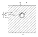
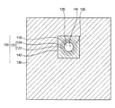
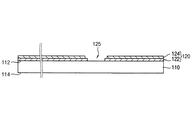
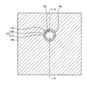
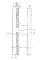
図1は、比較例に係るウィンドウ構造物を説明するための断面図であり、図2は、図1に示されるウィンドウ構造物の平面図である。この時、図1は、図2に示されたウィンドウ構造物のI−I’線に沿った断面図である。一方、図1には、ウィンドウ構造物に対応して配置されるカメラセンサーも共に示されている。 FIG. 1 is a cross-sectional view for explaining a window structure according to a comparative example, and FIG. 2 is a plan view of the window structure shown in FIG. At this time, FIG. 1 is a cross-sectional view taken along line I-I ′ of the window structure shown in FIG. 2. On the other hand, FIG. 1 also shows a camera sensor arranged corresponding to the window structure.
図1及び図2を参照すれば、ウィンドウ構造物50は、ウィンドウ10と、ウィンドウ10上に順次に積層されたデザイン層構造物20及び光遮蔽層30を含む。
Referring to FIGS. 1 and 2, the
ウィンドウ10は、ガラス、プラスチックなどの透明物質を含む。
The
デザイン層構造物20は、ウィンドウ10上に順次に積層された第1デザイン層22及び第2デザイン層24を含む。第1デザイン層22及び第2デザイン層24は、有彩色または白色の印刷層であることができる。デザイン層構造物20は、ウィンドウ10の上面の一部を露出させる第1ホール25を有する。デザイン層構造物20が第1デザイン層22及び第2デザイン層24を含むことによって、第1ホール25は、ウィンドウ10の上面から遠ざかるほど直径が増加する階段形状を有することができる。また、第1ホール25は、上面から見たとき、円形であることができる。
The
光遮蔽層30は、黒色または灰色の印刷層であることができる。光遮蔽層30は、第1ホール25に連通する第2ホール35を有し、第2ホール35は、第1ホール25よりも大きな直径を有する。第2ホール35は、上面から見たとき、円形状の第1ホール25と同心円形状を有する。
The
第1ホール25及び第2ホール35に対向してカメラセンサー90が配置される。カメラセンサー90は、基板80上に形成されることができる。
A
撮影物(図示せず)から反射してウィンドウ10及びデザイン層構造物20の第1ホール25を通過した光は、カメラセンサー90に入射することができ、前記光の一部は、カメラセンサー90から反射して光遮蔽層30及びデザイン層構造物20に入射する。この時、デザイン層構造物20に入射した光の一部は、再び反射されてカメラセンサー90に入射することができる。これによって、カメラセンサー90は、前記撮影物の色(色相)とは無関係にデザイン層構造物20の色を一部感知する。
Light reflected from a photographed object (not shown) and passed through the
また、デザイン層構造物20が非常に薄い厚さを有する場合、前記撮影物から反射してウィンドウ10を通過した後、デザイン層構造物20に入射した光の一部は、これを通過して第2ホール35を経てカメラセンサー90に入射することができる。この時、カメラセンサー90は、やはりデザイン層構造物20の色を感知することができる。ただし、光遮蔽層30によって覆われるデザイン層構造物20部分に入射した光は、デザイン層構造物20の厚さが比較的薄くても光遮蔽層30によって通過できないので、カメラセンサー90に入射できない。
Further, when the
結局、ウィンドウ10を通過した光が光遮蔽層30によって覆われていないデザイン層構造物20により乱反射されて、撮影物の色とは無関係な色がカメラセンサー90によって一部感知されることがあり、これによって、前記撮影物の周辺でデザイン層構造物20の色が現れる現象、即ち、一種のビネッティング(vignetting)現象が発生し得る。
Eventually, the light that has passed through the
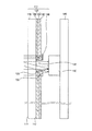
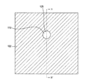
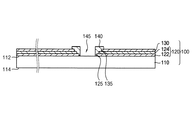
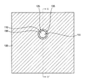
図3は、本発明の一実施形態に係るウィンドウ構造物を説明するための断面図であり、図4は、図3に示されるウィンドウ構造物の平面図である。この時、図3は、図4に示されたウィンドウ構造物のII−II’線に沿った断面図である。一方、図3には、ウィンドウ構造物に対応して配置されるカメラセンサーも共に示されている。 FIG. 3 is a cross-sectional view for explaining a window structure according to an embodiment of the present invention, and FIG. 4 is a plan view of the window structure shown in FIG. 3 is a cross-sectional view taken along the line II-II 'of the window structure shown in FIG. On the other hand, FIG. 3 also shows a camera sensor arranged corresponding to the window structure.
図3及び図4を参照すれば、ウィンドウ構造物100は、ウィンドウ110と、ウィンドウ110上に順次に積層された第1デザイン層構造物120及び第1光遮蔽層130と、第1光吸収層140を含む。
Referring to FIGS. 3 and 4, the
ウィンドウ110は、平板形状を有し、第1面112及び第1面112の反対面である第2面114を有する。ウィンドウ110は、光透過性物質、例えば、アクリルのような合成樹脂、ガラスなどを含む。
The
第1デザイン層構造物120は、ウィンドウ110の第1面112上に形成される。第1デザイン層構造物120は、順次に積層された第1デザイン層122及び第2デザイン層124を含む。この時、第1デザイン層122及び第2デザイン層124は、有彩色または白色の印刷層であることができる。また、第1デザイン122及び第2デザイン層124は、互いに同じ色を有することができる。
The first
第1デザイン層構造物120は、ウィンドウ110の第1面112の一部を露出させる第1ホール125を有する。第1ホール125は、上面から見たとき、円形であることができる。第1デザイン層構造物120が第1デザイン122及び第2デザイン層124を有することによって、第1ホール125は、ウィンドウ110の第1面112から遠ざかるほど直径が増加する階段形状を有する。即ち、第2デザイン層124は、第1デザイン層122の全部を覆っておらず、これによって、第1デザイン層122の一部が露出される。
The first
なお、図3及び図4では、第1デザイン層構造物120が、順次に積層された2つのデザイン層122,124を含む形態が示されているが、第1デザイン層構造物120は、3つ以上のデザイン層を含むこともできる。この時、前記デザイン層の側壁、及び/または、上面の一部によって定義される第1ホールは、ウィンドウ110の第1面112から遠ざかるほど直径が増加する階段形状を有することができる。これとは違って、第1デザイン層構造物120は、一つのデザイン層のみを含むこともできる。以下では、説明の便宜のために、第1デザイン層構造物120が2つのデザイン層を有する場合についてのみ説明する。
3 and 4, the first
第1光遮蔽層130は、第1デザイン層構造物120の第2デザイン層124上に形成され、第1ホール125に連通する第2ホール135を有する。第2ホール135は、第1ホール125よりも大きな直径を有し、上面から見たとき、円形の第1ホール125と同心円形状を有する。即ち、第1光遮蔽層130は、第2デザイン層124の全部を覆っておらず、これによって、第2デザイン層124の上面の一部が露出される。結局、第1ホール125及び第2ホール135から構成される第1ホール構造物は、ウィンドウ110の第1面112から遠ざかるほど直径が増加する階段形状を有する。第1光遮蔽層130は、黒色または灰色の印刷層であることができる。
The first
第1光吸収層140は、少なくとも第1ホール構造物、即ち、第1ホール125及び第2ホール135によって露出する第1デザイン層構造物120の部分を覆い、ウィンドウ110の第1面112の一部を露出させる第3ホール145を有する。即ち、第1光吸収層140は、第1ホール125により露出する、または、第1ホール125を画定する第1デザイン層122の側壁、第1デザイン層122の上面の一部、及び第2デザイン層124の側壁と、第2ホール135によって露出する第2デザイン層124の上面の一部を覆う。第3ホール145は、第1ホール125及び第2ホール135から構成された第1ホール構造物の内部に形成され、第1ホール構造物よりも小さな直径を有し、上面から見たとき、円形の第1ホール125または第2ホール135と同心円形状を有する。また、第3ホール145は、ウィンドウ110の第1面112に対して実質的に垂直な側壁を有する。即ち、第1光吸収層140は、ウィンドウ110の第1面112に対して実質的に垂直な側壁を有する。
The first
第1光吸収層140は、上述した第1デザイン層構造物120の部分だけでなく、第2ホール135によって露出される、または、第2ホール135を画定する第1光遮蔽層130の側壁と、第2ホール135に隣接した第1光遮蔽層130の上面の一部も覆う。この時、第1光吸収層140の外周は、上面から見たとき、円形の第1ホール125及び第2ホール135と同心円である。第1光吸収層140は、ウィンドウ110の第1面112に対して実質的に平行な上面を有する。第1光吸収層140は、黒色または灰色の印刷層であることができる。たとえば、第1光遮蔽層130は、灰色であり、第1光吸収層140は、黒色であることができる。
The first
図4では、第1デザイン層構造物120及び第1光遮蔽層130が第1〜第3ホール125,135,145の部分を除いて、ウィンドウ110の第1面112上に全面的に形成された形態を示しているが、所望のデザインに応じて第1デザイン層構造物120及び第1光遮蔽層130は、第1光吸収層140に隣接する部分上のみに形成されることもできる。
In FIG. 4, the first
第3ホール145に対向して、カメラセンサー190が配置される。カメラセンサー190は、基板180上に形成される。これによって、第3ホール145は、撮影物(図示せず)から反射された光がカメラセンサー190に入射する経路としての役割を果たす。
A
撮影物から反射してウィンドウ110及び第3ホール145を通過した光は、カメラセンサー190に入射し、前記光の一部は、カメラセンサー190から第1デザイン層構造物120、第1光遮蔽層130、または第1光吸収層140方向に反射する。しかし、第1光吸収層140が第1ホール125及び第2ホール135によって露出される第1デザイン層構造物120の部分を覆っているので、前記反射した光は、第1光吸収層140または第1光遮蔽層130により第1デザイン層構造物120に入射されることが遮断される。これによって、有彩色または白色の第1デザイン層構造物120の色が、カメラセンサー190によって感知されない。
The light reflected from the photographed object and passed through the
また、第1デザイン層構造物120が非常に薄い厚さを有する場合にも、前記撮影物から反射してウィンドウ110及び第1デザイン層構造物120を通過して第1ホール125または第2ホール135に進入する光は、第1光吸収層140により吸収されるので、カメラセンサー190に入射することができない。さらに、ウィンドウ110を通過して第1光遮蔽層130によって覆われる第1デザイン層構造物120の部分に入射された光は、第1光遮蔽層30によって遮断されるので、依然としてカメラセンサー190に入射することができない。
In addition, even when the first
従って、ウィンドウ110上に形成された第1デザイン層構造物120によって光が乱反射されて撮影物の色とは無関係な色がカメラセンサー190に入射されることが遮断されるので、前記撮影物周辺に第1デザイン層構造物120の色が現れるビネッティング現象を防止することができる。
Accordingly, light is irregularly reflected by the first
図5は、本発明の他の実施形態に係るウィンドウ構造物を説明するための平面図である。本実施形態に係るウィンドウ構造物は、光吸収層の外周形状を除いては、図3及び図4に示されたウィンドウ構造物と実質的に同一であるか、または、類似している。従って、同じ構成要素には同一参照符号を付与し、これに対する重複説明は省略する。 FIG. 5 is a plan view for explaining a window structure according to another embodiment of the present invention. The window structure according to the present embodiment is substantially the same as or similar to the window structure shown in FIGS. 3 and 4 except for the outer peripheral shape of the light absorption layer. Therefore, the same reference numerals are given to the same components, and redundant description thereof is omitted.
ウィンドウ構造物100は、ウィンドウ110と、ウィンドウ110上に順次に積層された第1デザイン層構造物120及び第1光遮蔽層130と、第2光吸収層142を含む。第2光吸収層142は、四角形の外形(外郭線)を有する。
The
なお、ウィンドウ構造物100は、図4及び図5に示した円形または四角形の外形を有する第1光吸収層140または第2光吸収層142以外に、楕円形などの曲線または多角形の外形を有する光吸収層を含むことができるのは当業者には自明である。以下では説明の便宜のために、円形の外形を有する第1光吸収層140を含むウィンドウ構造物についてのみ説明する。
Note that the
図6、図8、図10、及び図12は、図3及び図4に示されるウィンドウ構造物の製造方法を説明するための断面図であり、図7、図9、図11、及び図13は、ウィンドウ構造物の製造方法を説明するための平面図である。この時、図6、図8、図10、及び図12は、図7、図9、図11、及び図13に示されたウィンドウ構造物のIII−III’線に沿った断面図である。一方、図6〜図13は、例示的に図3及び図4に示したウィンドウ構造物を製造する方法を説明しているが、必ずしもこれに限定されるのではない。 6, 8, 10, and 12 are cross-sectional views for explaining a method of manufacturing the window structure shown in FIGS. 3 and 4, and FIGS. 7, 9, 11, and 13 are used. These are top views for demonstrating the manufacturing method of a window structure. 6, 8, 10, and 12 are cross-sectional views taken along the line III-III ′ of the window structure shown in FIGS. 7, 9, 11, and 13. Meanwhile, FIGS. 6 to 13 illustrate a method for manufacturing the window structure shown in FIGS. 3 and 4 exemplarily, but the method is not necessarily limited thereto.
図6及び図7を参照すれば、ウィンドウ110上に第1デザイン層122が形成される。
Referring to FIGS. 6 and 7, the
ウィンドウ110は、光透過性物質、例えば、アクリルのような合成樹脂、ガラスなどを含む。ウィンドウ110は、第1面112及び第1面112の反対面である第2面114を含む。
The
第1デザイン層122は、ウィンドウ110の第1面112上に形成される。第1デザイン層122は、メッシュ(mesh)を利用したスクリーン印刷工程を通じて形成することができる。即ち、ウィンドウ110の第1面112上に、所望のパターンを形成するためのメッシュ(図示せず)を配置し、前記メッシュ上にインクを噴射または滴下した後、ゴム板により前記噴射または滴下されたインク上部に圧力を加えて、所望のパターンを有する第1デザイン層122を形成することができる。第1デザイン層122は、有彩色または白色のインクを使って形成することができ、前記インクには、銀(sliver)等の金属粉末が含まれることができる。
The
第1デザイン層122は、内部に第1ホール125を有するように形成される。この時、第1ホール125は、上面から見たとき、円形である。
The
なお、ウィンドウ110の第1面112に第1デザイン層122が印刷された後、乾燥工程をさらに遂行することができる。
In addition, after the
図8及び図9を参照すれば、第1デザイン層122上に第2デザイン層124が形成される。
Referring to FIGS. 8 and 9, the
第2デザイン層124も、第1デザイン層122と同様に、メッシュを利用したスクリーン印刷工程を通じて形成することができる。第2デザイン層124は、有彩色または白色のインクを使って形成することができ、第1デザイン層122と同じ色のインクを使って形成することができる。
Similarly to the
第2デザイン層124は、内部にホールを有するように形成される。この時、前記ホールは、上面から見たとき、円形の第1ホール125と同心円形状である。これにより、第1ホール125と前記ホールは互いに連通することができる。
The
前記スクリーン印刷工程を遂行する間、第1ホール125によって露出されたウィンドウ110の第1面112部分に第2デザイン層124が形成されないように、前記ホールが第1ホール125よりも大きな直径を有するように形成される。これによって、第1デザイン層122は、第2デザイン層124によって全部覆われず、第1ホール125に隣接する第1デザイン層122部分が露出する。
During the screen printing process, the hole has a larger diameter than the
以下では、第1デザイン層122内部に形成された第1ホール125と、第2デザイン層124内部に形成されて第1ホール125に連通する前記ホールを、通称して第1ホール125と称する。この時、第1ホール125の底面は、第1デザイン層122によって覆われないウィンドウ110の第1面112部分により画定され、第1ホール125の側壁は、第1デザイン層122の側壁及び露出した上面の一部と、第2デザイン層124の側壁とにより画定される。これによって、第1ホール125は、ウィンドウ110の第1面112から遠ざかるほど直径が大きくなる階段形状を有する。
Hereinafter, the
第1デザイン層122及び第2デザイン層124は、共に第1デザイン層構造物120を形成する。上述した通り、第1デザイン層構造物120は、順次に積層された3つ以上のデザイン層を含むように形成されることもでき、または、第2デザイン層124は形成されず、第1デザイン層122のみを含むように形成されることもできる。
The
図10及び図11を参照すれば、第1デザイン層構造物120の上面に、即ち、第2デザイン層124上に第1光遮蔽層130が形成される。
Referring to FIGS. 10 and 11, the first
第1光遮蔽層130も、第1デザイン122及び第2デザイン層124と同様に、メッシュを利用したスクリーン印刷工程を通じて形成することができる。第1光遮蔽層130は、黒色または灰色インクを使って形成することができる。
Similarly to the
第1光遮蔽層130は、内部に第2ホール135を有するように形成される。この時、第2ホール135は、上面から見たとき、円形の第1ホール125と同心円形状を有する。これによって、第1ホール125と第2ホール135とは、互いに連通することができる。
The first
前記スクリーン印刷工程を遂行する間、第1ホール125によって露出したウィンドウ110の第1面112部分に第1光遮蔽層130が形成されないように、第2ホール135は、第1ホール125よりも大きな直径を有するように形成される。これによって、第2デザイン層124は、第1光遮蔽層130により全部覆われず、第1ホール125に隣接する第2デザイン層124の上面の部分が露出する。
During the screen printing process, the
以下では、第1ホール125とこれに連通する第2ホール135を通称して第1ホール構造物と称する。この時、第1ホール構造物の側壁は、上述した第1ホール125の側壁、第1ホール125に隣接して露出した第2デザイン層124の上面の部分、及び第1光遮蔽層130の側壁によって画定される。これによって、第1ホール構造物は、ウィンドウ110の第1面112から遠ざかるほど直径が大きくなる階段形状を有する。
Hereinafter, the
図12及び図13を参照すれば、少なくとも第1ホール構造物、即ち、第1ホール125及び第2ホール135により露出する第1デザイン層構造物120部分を覆うように、第1光吸収層140がウィンドウ110の第1面112上に形成され、これにより、ウィンドウ構造物100が製造される。
Referring to FIGS. 12 and 13, the first
第1光吸収層140も、デザイン層122,124及び第1光遮蔽層130と同様に、メッシュを利用したスクリーン印刷工程を通じて形成することができる。第1光吸収層140は、黒色または灰色インクを使って形成することができる。
Similarly to the design layers 122 and 124 and the first
第1光吸収層140の外形は、上面から見たとき、円形であり、第1光吸収層140は、ウィンドウ110の第1面112の一部を露出させる第3ホール145を有する。しかし、上述した通り、第1光吸収層140は、上面から見たとき、楕円形などの曲線または多角形の外形を有するように形成されることもできる。
The outer shape of the first
第1光吸収層140は、少なくとも第1ホール125によって露出される、または、第1ホール125を画定する第1デザイン層122の側壁、第1デザイン層122上面の一部、及び第2デザイン層124の側壁と、第2ホール135によって露出する第2デザイン層124上面の一部を覆う。さらに、第1光吸収層140は、第2ホール135によって露出される、または、第2ホール135を画定する第1光遮蔽層130の側壁と、第2ホール135に隣接した第1光遮蔽層130上面の一部も覆うように形成される。
The first
なお、第3ホール145は、第1ホール構造物の内部に形成されて前記第1ホール構造物よりも小さな直径を有し、上面から見たとき、円形の第1ホール125および第2ホール135と同心円形状を有する。第3ホール145は、ウィンドウ110の第1面112に対して実質的に垂直な側壁を有する。即ち、第1光吸収層140は、ウィンドウ110の第1面112に対して実質的に垂直な側壁を有するように形成される。第1光吸収層140は、ウィンドウ110の第1面112に対して実質的に平行な上面を有するように形成される。
The
図14〜図19は、本発明のさらに他の実施形態に係るウィンドウ構造物を説明するための断面図である。図14〜図19に示されたウィンドウ構造物は、光吸収層の形状を除いては、図3及び図4に示されたウィンドウ構造物と実質的に同一であるか、または、類似している。従って、同じ構成要素には同じ参照符号を付与し、これに対する重複説明は省略する。 14 to 19 are cross-sectional views for explaining a window structure according to still another embodiment of the present invention. The window structure shown in FIGS. 14 to 19 is substantially the same as or similar to the window structure shown in FIGS. 3 and 4 except for the shape of the light absorption layer. Yes. Therefore, the same reference numerals are given to the same components, and redundant description thereof is omitted.
図14を参照すれば、ウィンドウ構造物100は、ウィンドウ110と、ウィンドウ110上に順次に積層された第1デザイン層構造物120及び第1光遮蔽層130と、第3光吸収層144を含む。
Referring to FIG. 14, the
第3光吸収層144は、ウィンドウ110の第1面112に対して垂直でなく、傾斜した側壁を有する。具体的に、第3光吸収層144が有する第3ホール145は、ウィンドウ110の第1面112から遠ざかるにつれて次第に増加する直径を有する。これによって、撮影物から反射されてウィンドウ110を通過しカメラセンサー190に入射する光量が、相対的に増加することができる。なお、第3光吸収層144は、ウィンドウ110の第1面112に対して実質的に平行な上面を有する。
The third
図15を参照すれば、ウィンドウ構造物100は、ウィンドウ110と、ウィンドウ110上に順次に積層された第1デザイン層構造物120及び第1光遮蔽層130と、第4光吸収層146を含む。
Referring to FIG. 15, the
第4光吸収層146は、ウィンドウ110の第1面112に対して傾斜した側壁及びウィンドウ110の第1面112に対して平行でない上面を有する。具体的には、第4光吸収層146は、全体的に曲線(曲面)状の側壁及び上面を有する。これによって、第4光吸収層146内部の第3ホール145も、曲線状の側壁を有することができる。
The fourth
図16を参照すれば、ウィンドウ構造物100は、ウィンドウ110と、ウィンドウ110上に順次に積層された第1デザイン層構造物120及び第1光遮蔽層130と、第5光吸収層148を含む。
Referring to FIG. 16, the
第5光吸収層148は、ウィンドウ110の第1面112に対して垂直な側壁及びウィンドウ110の第1面112に対して平行な上面を有し、第1光遮蔽層130の上面を覆わない。第5光吸収層148の上面は、第1光遮蔽層130の上面よりも高い。
The fifth
図17を参照すれば、ウィンドウ構造物100は、ウィンドウ110と、ウィンドウ110上に順次に積層された第1デザイン層構造物120及び第1光遮蔽層130と、第6光吸収層150を含む。
Referring to FIG. 17, the
第6光吸収層150は、ウィンドウ110の第1面112に対して垂直な側壁及びウィンドウ110の第1面112に対して平行な上面を有し、第1光遮蔽層130の上面を覆わない。第6光吸収層150の上面は、第1光遮蔽層130の上面と実質的に同じ高さを有する。
The sixth
図18を参照すれば、ウィンドウ構造物100は、ウィンドウ110と、ウィンドウ110上に順次に積層された第1デザイン層構造物120及び第1光遮蔽層130と、第7光吸収層152を含む。
Referring to FIG. 18, the
第7光吸収層152は、ウィンドウ110の第1面112に対して傾斜した曲面状の側壁を有し、第1光遮蔽層130の上面を覆わない。第7光吸収層152は、第1光遮蔽層130の上面と実質的に同一であるか、または、低い高さにのみ形成される。
The seventh
図19を参照すれば、ウィンドウ構造物100は、ウィンドウ110と、ウィンドウ110上に順次に積層された第1デザイン層構造物120及び第1光遮蔽層130と、第8光吸収層154を含む。
Referring to FIG. 19, the
第8光吸収層154は、ウィンドウ110の第1面112に対して傾斜した曲面状の側壁を有し、第1光遮蔽層130の上面を覆わない。第8光吸収層154は、第1光遮蔽層130の側壁の一部のみを覆う。
The eighth
図20は、本発明のさらに他の実施形態に係るウィンドウ構造物を説明するための断面図であり、図21は、図20に示されるウィンドウ構造物の平面図である。この時、図20は、図21に示されたウィンドウ構造物のIV−IV’線に沿った断面図である。図20及び図21に示したウィンドウ構造物は、別途の光吸収層を含まず、光遮蔽層の形状が違うということを除けば、図3及び図4に示したウィンドウ構造物と実質的に同一であるか、または、類似している。従って、同じ構成要素には同じ参照符号を付与し、これに対する重複説明は省略する。一方、図20には、ウィンドウ構造物に対応して配置されるカメラセンサーも共に示されている。 20 is a cross-sectional view for explaining a window structure according to still another embodiment of the present invention, and FIG. 21 is a plan view of the window structure shown in FIG. At this time, FIG. 20 is a cross-sectional view taken along line IV-IV ′ of the window structure shown in FIG. 21. The window structure shown in FIGS. 20 and 21 does not include a separate light absorption layer and is substantially the same as the window structure shown in FIGS. 3 and 4 except that the shape of the light shielding layer is different. Identical or similar. Therefore, the same reference numerals are given to the same components, and redundant description thereof is omitted. On the other hand, FIG. 20 also shows a camera sensor arranged corresponding to the window structure.
図20及び図21を参照すれば、ウィンドウ構造物100は、ウィンドウ110と、ウィンドウ110上に順次に積層された第1デザイン層構造物120及び第2光遮蔽層132を含む。
Referring to FIGS. 20 and 21, the
第2光遮蔽層132は、第1デザイン層構造物120を覆いつつウィンドウ110上に形成される。この時、第2光遮蔽層132は、第1ホール125内部に形成されてウィンドウ110の第1面112の一部を露出させる第4ホール137を含む。第4ホール137は、上面から見たとき、円形の第1ホール125と同心円形状を有する。
The second
第4ホール137は、ウィンドウ110の第1面112に対して実質的に垂直な側壁を有する。即ち、第2光遮蔽層132は、ウィンドウ110の第1面112に対して実質的に垂直な側壁を有する。
The
第2光遮蔽層132は、黒色または灰色の印刷層であることができる。第2光遮蔽層132が第1デザイン層構造物120を覆うので、第1デザイン層構造物120により光が乱反射されて撮影物の色とは無関係な色がカメラセンサー190に入射されることが防止され、ビネッティング現象を防止することができる。即ち、第2光遮蔽層132は、図3及び図4を参照して説明したウィンドウ構造物の第1光遮蔽層130及び第1光吸収層140の機能を同時に遂行することができる。
The second
図22及び図23は、本発明のさらに他の実施形態に係るウィンドウ構造物を説明するための断面図である。図22及び図23に示されたウィンドウ構造物は、光遮蔽層の側壁の形状を除いては、図20及び図21に示されたウィンドウ構造物と実質的に同一であるか、または、類似している。従って、同じ構成要素には同じ参照符号を付与し、これに対する重複説明は省略する。 22 and 23 are cross-sectional views for explaining a window structure according to still another embodiment of the present invention. The window structure shown in FIGS. 22 and 23 is substantially the same as or similar to the window structure shown in FIGS. 20 and 21 except for the shape of the side wall of the light shielding layer. doing. Therefore, the same reference numerals are given to the same components, and redundant description thereof is omitted.
図22を参照すれば、ウィンドウ構造物100は、ウィンドウ110と、ウィンドウ110上に順次に積層された第1デザイン層構造物120及び第3光遮蔽層134を含む。
Referring to FIG. 22, the
第3光遮蔽層134は、ウィンドウ110の第1面112に対して垂直でない傾斜した側壁を有する。これによって、ウィンドウ110を通過し、第4ホール137を通じてカメラセンサー190に入射する光の光量が増加することができる。
The third light shielding layer 134 has inclined sidewalls that are not perpendicular to the
図23を参照すれば、ウィンドウ構造物100は、ウィンドウ110と、ウィンドウ110上に順次に積層された第1デザイン層構造物120及び第4光遮蔽層136を含む。
Referring to FIG. 23, the
第4光遮蔽層136は、ウィンドウ110の第1面112に対して垂直でない傾斜した側壁を有し、前記側壁は曲面である。
The fourth light shielding layer 136 has inclined sidewalls that are not perpendicular to the
図24は、本発明のさらに他の実施形態に係るウィンドウ構造物を説明するための断面図であり、図25は、図24に示されるウィンドウ構造物の平面図である。この時、図24は、図25に示されたウィンドウ構造物のV−V’線に沿った断面図である。図24には、ウィンドウ構造物に対応して配置されるカメラセンサーも共に示されている。図24に示されたウィンドウ構造物は、デザイン層構造物、光吸収層、及び光遮蔽層の形状を除いては、図3及び図4に示されたウィンドウ構造物と実質的に同一であるか、または、類似している。従って、同じ構成要素には同じ参照符号を付与し、これに対する重複説明は省略する。 FIG. 24 is a cross-sectional view for explaining a window structure according to still another embodiment of the present invention, and FIG. 25 is a plan view of the window structure shown in FIG. 24 is a cross-sectional view taken along the line V-V ′ of the window structure shown in FIG. FIG. 24 also shows a camera sensor arranged corresponding to the window structure. The window structure shown in FIG. 24 is substantially the same as the window structure shown in FIGS. 3 and 4 except for the shape of the design layer structure, the light absorption layer, and the light shielding layer. Or similar. Therefore, the same reference numerals are given to the same components, and redundant description thereof is omitted.
図24及び図25を参照すれば、ウィンドウ構造物100は、ウィンドウ110と、ウィンドウ110上に順次に積層された第2デザイン層構造物121及び第5光遮蔽層133と、第9光吸収層156を含む。
Referring to FIGS. 24 and 25, the
第2デザイン層構造物121は、ウィンドウ110の第1面112上に順次に積層された第1デザイン層122及び第3デザイン層123を含む。この時、第3デザイン層123は、第1デザイン層122の全面を覆う。これによって、第2デザイン層構造物121が有する第5ホール127は、ウィンドウ110の第1面112からの離隔距離に関係なく一定の直径を有する。
The second
第5光遮蔽層133は、第2デザイン層構造物121の上面、即ち、第3デザイン層123上に形成され、第3デザイン層123の全面を覆う。従って、第5光遮蔽層133が有する第6ホール139は、第5ホール127と実質的に同じ直径を有する。結局、第5ホール127及び第6ホール139から構成される第2ホール構造物は、ウィンドウ110の第1面112からの離隔距離に関係なく一定の直径を有する。
The fifth
第9光吸収層156は、少なくとも第5ホール127により露出する第2デザイン層構造物121部分、即ち、第1及び第3デザイン層122,123の側壁を覆い、ウィンドウ110の第1面112の一部を露出させる第7ホール155を有する。この時、第7ホール155は、第5及び第6ホール127,139から構成された第2ホール構造物の内部に形成され、第2ホール構造物よりも小さな直径を有し、上面から見たとき、円形の第5ホール127または第6ホール139と同心円形状を有する。第7ホール155は、ウィンドウ110の第1面112に対して実質的に垂直な側壁を有する。即ち、第9光吸収層156は、ウィンドウ110の第1面112に対して実質的に垂直な側壁を有する。
The ninth
第9光吸収層156は、上述した第2デザイン層構造物121の一部だけでなく、第6ホール139により露出する、または、第6ホール139を画定する第5光遮蔽層133の側壁及び第6ホール139に隣接した第5光遮蔽層133上面の一部を覆う。この時、第9光吸収層156の外形は、上面から見たとき、円形の第5及び第6ホール127,139と同心円である。第9光吸収層156は、ウィンドウ110の第1面112に対して実質的に平行な上面を有する。
The ninth
図26は、本発明のさらに他の実施形態に係るウィンドウ構造物を説明するための断面図である。図26に示したウィンドウ構造物は、印刷膜をさらに含むということを除いては、図3及び図4に示されたウィンドウ構造物と実質的に同一であるか、または、類似している。従って、同じ構成要素には同じ参照符号を付与し、これに対する重複説明は省略する。 FIG. 26 is a cross-sectional view for explaining a window structure according to still another embodiment of the present invention. The window structure shown in FIG. 26 is substantially the same as or similar to the window structure shown in FIGS. 3 and 4 except that it further includes a printed film. Therefore, the same reference numerals are given to the same components, and redundant description thereof is omitted.
図26を参照すれば、ウィンドウ構造物100は、ウィンドウ110と、ウィンドウ110の第1面112上に形成されたPETフィルム170と、PETフィルム170上に順次に積層された第1デザイン層構造物120及び第1光遮蔽層130と、第1光吸収層140を含む。
Referring to FIG. 26, the
第1デザイン層構造物120は、PETフィルム170の上面の一部を露出させる第1ホール125を有し、第1光遮蔽層130は、第1ホール125に連通する第2ホール135を有する。第1光吸収層140は、少なくとも第1ホール125及び第2ホール135により露出する第1デザイン層構造物120の部分を覆い、PETフィルム170上面の一部を露出させる第3ホール145を有する。
The first
ウィンドウ110の第1面112上に光透過性PETフィルム170が形成されることによって、カメラセンサー190に入射する光の光量には影響を与えずに、第1デザイン構造物120を容易に高品質に印刷することができる。
By forming the light transmissive PET film 170 on the
図27は、本発明のさらに他の実施形態に係るウィンドウ構造物を含むカメラが搭載された電子装置を説明するための断面図である。前記電子装置は、図3及び図4を参照して説明したウィンドウ構造物及びカメラセンサーを含むので、これに対する詳しい説明は省略する。 FIG. 27 is a cross-sectional view illustrating an electronic apparatus equipped with a camera including a window structure according to still another embodiment of the present invention. Since the electronic apparatus includes the window structure and the camera sensor described with reference to FIGS. 3 and 4, a detailed description thereof will be omitted.
図27を参照すれば、前記電子装置は、基板180と、表示パネル200と、フレキシブル回路基板(Flexible Printed Circuit Board:FPCB)220と、ウィンドウ構造物100と、カメラセンサー190を含む。
Referring to FIG. 27, the electronic apparatus includes a
基板180は、前記電子装置を駆動するための各種回路配線を含む。基板180は、プリント回路基板(Printed Circuit Board:PCB)であることができる。
The
表示パネル200は、例えば、有機発光表示パネル(OLED display panel)、液晶表示パネル(LCD panel)、プラズマ表示パネル(PDP)等である。表示パネル200が、液晶表示パネルの場合、前記電子装置は、液晶表示パネルに光を提供するバックライトアセンブリーをさらに含むことができる。表示パネル200は、クッションテープのような接着剤210によって基板180に接着される。
The
フレキシブル回路基板220は、基板180に接続されて表示パネル200を駆動するための駆動信号を表示パネル200に提供する。フレキシブル回路基板220は、表示パネル200の第1面に接触し、表示パネル200に対向する基板180の第1面に向かって曲げられることができる。これとは違って、フレキシブル回路基板220は、表示パネル200の第1面に接触し、基板180の第1面の反対面の第2面に向かって曲げられることもできる。図27では、フレキシブル回路基板220が基板180の第2面に向かって曲げられている形態が示されている。フレキシブル回路基板220は、例えば、柔軟性を有する樹脂を含む。
The
ウィンドウ構造物100は、表示パネル200の第1面の反対面である第2面の上部に形成される。ウィンドウ構造物100は、光透過性接着剤230、例えば、SVR(Super View Resin)のような接着剤によって表示パネル200に接着される。
The
カメラセンサー190は、ウィンドウ構造物100の第3ホール145に対向して配置され、例えば、カメラコンテナ185によって基板180上に配置される。
The
前記電子装置に搭載されるカメラのカメラセンサー190は、第1デザイン層構造物120を含むウィンドウ構造物100の第3ホール145に対向して配置され、ウィンドウ構造物100が第1光吸収層140を含むことによってビネッティング現象を防止することができる。
The
図28及び図29は、図27に示されるウィンドウ構造物を含むカメラが搭載された電子装置を製造する方法を説明するための断面図である。図28及び図29は、例示的に図27に示された電子装置を製造する方法を説明しているが、必ずしもこれに限定されるものではない。 28 and 29 are cross-sectional views for explaining a method of manufacturing an electronic device on which a camera including the window structure shown in FIG. 27 is mounted. 28 and 29 illustrate a method for manufacturing the electronic device shown in FIG. 27 by way of example, but the present invention is not necessarily limited to this.
図28を参照すれば、図6〜図13を参照して説明した工程と実質的に同一であるか、または、類似の工程を遂行してウィンドウ構造物100を製造することができる。
Referring to FIG. 28, the
図29を参照すれば、基板180の第1面上にカメラコンテナ185を配置し、カメラコンテナ185にカメラセンサー190を実装する。また、基板180の第1面上に表示パネル200を接着する。クッションテープのような接着剤210によって、基板180の第1面と表示パネル200の第1面とが相互に接着される。
Referring to FIG. 29, the
以後、フレキシブル回路基板220を表示パネル200の第1面に接着させ、基板180の第1面、または、前記第1面の反対面である第2面に向けて曲げる。図29では、フレキシブル回路基板220が、基板180の第2面に曲げられる形態が示されている。
Thereafter, the
再び図27を参照すれば、ウィンドウ構造物100の第1光遮蔽層130上に、例えば、SVRのような光透過性接着剤230を塗布し、ウィンドウ構造物100を表示パネル200の第2面に接着させることによって前記電子装置を製造することができる。この時、ウィンドウ構造物100の第3ホール145が基板180上に配置されたカメラセンサー190に対向するように、ウィンドウ構造物100が接着される。
Referring to FIG. 27 again, a light-transmitting adhesive 230 such as SVR is applied on the first
図30は、本発明のさらに他の実施形態に係るウィンドウ構造物を含むカメラが搭載された電子装置を説明するための断面図である。図30の電子装置は、ウィンドウ構造物の構成を除けば、図27の電子装置と実質的に同一であるか、または、類似している。具体的には、図30の電子装置は、図20を参照して説明したウィンドウ構造物と実質的に同じウィンドウ構造物を含む。即ち、本実施形態に係る電子装置に含まれたウィンドウ構造物は、ウィンドウ110、第1デザイン層構造物120及び第2光遮蔽層132を含む。同じ構成要素には同じ参照符号を付与し、これに対する重複説明は省略する。
FIG. 30 is a cross-sectional view illustrating an electronic apparatus equipped with a camera including a window structure according to still another embodiment of the present invention. The electronic device of FIG. 30 is substantially the same as or similar to the electronic device of FIG. 27 except for the configuration of the window structure. Specifically, the electronic device of FIG. 30 includes a window structure that is substantially the same as the window structure described with reference to FIG. That is, the window structure included in the electronic device according to the present embodiment includes the
以上、添付図面を参照しながら本発明の好適な実施形態について詳細に説明したが、本発明は上記の実施形態に限定されない。本発明の属する技術の分野における通常の知識を有する者であれば、特許請求の範囲に記載された技術的思想の範囲内において、各種の変更例または修正例に想到し得ることは明らかであり、これらについても、当然に本発明の技術的範囲に属するものと理解される。 The preferred embodiments of the present invention have been described in detail above with reference to the accompanying drawings, but the present invention is not limited to the above-described embodiments. It is obvious that a person having ordinary knowledge in the technical field to which the present invention pertains can come up with various changes and modifications within the scope of the technical idea described in the claims. These are naturally understood to belong to the technical scope of the present invention.
本発明のウィンドウ構造物は、表示パネルを含み、カメラが搭載されるすべての電子機器に適用されることができる。 The window structure of the present invention includes a display panel and can be applied to all electronic devices on which a camera is mounted.
10,110 ウィンドウ、
20,120,121 デザイン層構造物、
22,24,122,123,124 デザイン層、
25,35,125,127,135,137,139,145,155 ホール、
30,130,132,133,134,136 光遮蔽層、
50,100 ウィンドウ構造物、
80,180 基板、
90,190 カメラセンサー、
140,142,144,146,148,150,152,154,156 光吸収層、
185 カメラコンテナ、
200 表示パネル、
210 接着剤、
220 フレキシブル回路基板、
230 光透過性接着剤。
10,110 windows,
20, 120, 121 design layer structure,
22, 24, 122, 123, 124 design layer,
25, 35, 125, 127, 135, 137, 139, 145, 155 holes,
30, 130, 132, 133, 134, 136 light shielding layer,
50,100 window structure,
80, 180 substrates,
90,190 Camera sensor,
140, 142, 144, 146, 148, 150, 152, 154, 156 light absorption layer,
185 camera container,
200 display panel,
210 adhesive,
220 flexible circuit board,
230 Light transmissive adhesive.
Claims (39)
前記ウィンドウ上に形成され、当該ウィンドウの一部を露出させる第1ホールを有するデザイン層構造物と、
前記デザイン層構造物上に形成され、前記第1ホールに連通する第2ホールを有する光遮蔽層と、
前記第1及び第2ホールによって露出する前記デザイン層構造物の部分を少なくとも覆い、前記ウィンドウの一部を露出させる第3ホールを有する光吸収層と、
を含むことを特徴とするウィンドウ構造物。 Window and
A design layer structure formed on the window and having a first hole exposing a part of the window;
A light shielding layer formed on the design layer structure and having a second hole communicating with the first hole;
A light absorption layer having a third hole that covers at least a portion of the design layer structure exposed by the first and second holes and exposes a part of the window;
The window structure characterized by including.
前記デザイン層構造物は、前記PETフィルム上に形成されることを特徴とする請求項1〜15のいずれか1項に記載のウィンドウ構造物。 Further comprising a PET film formed on the window;
The window structure according to claim 1, wherein the design layer structure is formed on the PET film.
前記デザイン層構造物上に、前記第1ホールに連通する第2ホールを有する光遮蔽層を形成する段階と、
前記第1及び第2ホールによって露出する前記デザイン層構造物の部分を少なくとも覆い、前記ウィンドウの一部を露出させる第3ホールを有する光吸収層を形成する段階と、
を含むことを特徴とするウィンドウ構造物の製造方法。 Forming a design layer structure having a first hole exposing a part of the window on the window;
Forming a light shielding layer having a second hole communicating with the first hole on the design layer structure;
Forming a light absorption layer having a third hole covering at least a portion of the design layer structure exposed by the first and second holes and exposing a part of the window;
The manufacturing method of the window structure characterized by including.
前記ウィンドウ上に形成され、当該ウィンドウの一部を露出させる第1ホールを有するデザイン層構造物と、
前記ウィンドウ上に形成され、前記デザイン層構造物を覆いつつ、前記ウィンドウの一部を露出させる第2ホールを有する光遮蔽層と、
を含むことを特徴とするウィンドウ構造物。 Window and
A design layer structure formed on the window and having a first hole exposing a part of the window;
A light shielding layer having a second hole formed on the window and covering the design layer structure and exposing a part of the window;
The window structure characterized by including.
前記表示パネル上に形成され、ウィンドウと、前記ウィンドウ上に形成され当該ウィンドウの一部を露出させる第1ホールを有するデザイン層構造物と、前記デザイン層構造物上に形成され前記第1ホールに連通する第2ホールを有する光遮蔽層と、前記第1及び第2ホールによって露出する前記デザイン層構造物の部分を少なくとも覆い前記ウィンドウの一部を露出させる第3ホールを有する光吸収層と、を含むウィンドウ構造物と、
前記ウィンドウ構造物と前記基板との間に配置され、前記第3ホールを通過する光を感知するカメラセンサーと、
を含むことを特徴とするカメラが搭載された電子装置。 A display panel formed on a substrate;
A design layer structure formed on the display panel and having a window, a first hole formed on the window and exposing a part of the window, and a first layer formed on the design layer structure. A light shielding layer having a second hole that communicates, a light absorbing layer having a third hole that covers at least a portion of the design layer structure exposed by the first and second holes and exposes a part of the window; A window structure including
A camera sensor disposed between the window structure and the substrate and sensing light passing through the third hole;
An electronic device equipped with a camera characterized by comprising:
前記デザイン層構造物は、前記ウィンドウの前記第1面上に形成されることを特徴とする請求項29〜35のいずれか1項に記載の電子装置。 The window has a first surface facing the substrate and a second surface that is the opposite surface of the first surface;
36. The electronic device according to claim 29, wherein the design layer structure is formed on the first surface of the window.
前記表示パネルと離隔されるカメラセンサーを前記基板上に形成する段階と、
ウィンドウ上に当該ウィンドウの一部を露出させる第1ホールを有するデザイン層構造物を形成し、前記デザイン層構造物上に前記第1ホールに連通する第2ホールを有する光遮蔽層を形成し、前記第1及び第2ホールによって露出する前記デザイン層構造物の部分を少なくとも覆い前記ウィンドウの一部を露出させる第3ホールを有する光吸収層を形成して、ウィンドウ構造物を形成する段階と、
前記第3ホールが前記カメラセンサーと重なり、前記デザイン層構造物が前記基板に対向するように、前記ウィンドウ構造物を前記表示パネルに接着する段階と、
を含むことを特徴とするカメラが搭載された電子装置の製造方法。 Forming a display panel on a substrate;
Forming a camera sensor spaced apart from the display panel on the substrate;
Forming a design layer structure having a first hole exposing a part of the window on the window, and forming a light shielding layer having a second hole communicating with the first hole on the design layer structure; Forming a light absorbing layer having a third hole covering at least a portion of the design layer structure exposed by the first and second holes and exposing a part of the window, thereby forming a window structure;
Adhering the window structure to the display panel such that the third hole overlaps the camera sensor and the design layer structure faces the substrate;
The manufacturing method of the electronic device carrying the camera characterized by the above-mentioned.
前記表示パネル上に形成され、ウィンドウと、前記ウィンドウ上に形成され当該ウィンドウの一部を露出させる第1ホールを有するデザイン層構造物と、前記ウィンドウ上に形成され前記デザイン層構造物を覆いつつ前記ウィンドウの一部を露出させる第2ホールを有する光遮蔽層と、を含むウィンドウ構造物と、
前記ウィンドウ構造物と前記基板との間に配置され、前記第2ホールを通過する光を感知するカメラセンサーと、
を含むことを特徴とするカメラが搭載された電子装置。 A display panel formed on a substrate;
A design layer structure formed on the display panel and having a window, a first hole formed on the window and exposing a part of the window, and a design layer structure formed on the window and covering the design layer structure A light shielding layer having a second hole exposing a part of the window, and a window structure including:
A camera sensor which is disposed between the window structure and the substrate and senses light passing through the second hole;
An electronic device equipped with a camera characterized by comprising:
Applications Claiming Priority (2)
| Application Number | Priority Date | Filing Date | Title |
|---|---|---|---|
| KR1020120054731A KR102031654B1 (en) | 2012-05-23 | 2012-05-23 | Window structure, method of manufacturing the same, electronic device equipped with a camera including a window structure and method of manufacturing the same |
| KR10-2012-0054731 | 2012-05-23 |
Publications (2)
| Publication Number | Publication Date |
|---|---|
| JP2013247672A true JP2013247672A (en) | 2013-12-09 |
| JP6247005B2 JP6247005B2 (en) | 2017-12-13 |
Family
ID=48747295
Family Applications (1)
| Application Number | Title | Priority Date | Filing Date |
|---|---|---|---|
| JP2013010361A Active JP6247005B2 (en) | 2012-05-23 | 2013-01-23 | Window structure, manufacturing method thereof, electronic device mounted with camera, and manufacturing method thereof |
Country Status (6)
| Country | Link |
|---|---|
| US (3) | US9640681B2 (en) |
| EP (1) | EP2667236B1 (en) |
| JP (1) | JP6247005B2 (en) |
| KR (1) | KR102031654B1 (en) |
| CN (3) | CN103424957B (en) |
| TW (1) | TWI580270B (en) |
Cited By (4)
| Publication number | Priority date | Publication date | Assignee | Title |
|---|---|---|---|---|
| KR20180102806A (en) * | 2017-03-08 | 2018-09-18 | 삼성전자주식회사 | Electronic apparatus including optical sensor module |
| JP2019534476A (en) * | 2016-10-20 | 2019-11-28 | スリーエム イノベイティブ プロパティズ カンパニー | Optical window camouflage device |
| US10983652B2 (en) | 2018-04-13 | 2021-04-20 | Samsung Electronics Co., Ltd. | Display having opaque member disposed in area surrounded by pixels and electronic apparatus having the same |
| JP7441918B2 (en) | 2019-12-03 | 2024-03-01 | エルジー ディスプレイ カンパニー リミテッド | display device |
Families Citing this family (47)
| Publication number | Priority date | Publication date | Assignee | Title |
|---|---|---|---|---|
| KR102031654B1 (en) * | 2012-05-23 | 2019-10-15 | 삼성디스플레이 주식회사 | Window structure, method of manufacturing the same, electronic device equipped with a camera including a window structure and method of manufacturing the same |
| CN104635969A (en) * | 2013-11-14 | 2015-05-20 | 索尼公司 | Touch screen, electronic equipment and method for preventing touch screen from light leakage |
| KR102408239B1 (en) * | 2015-09-28 | 2022-06-14 | 애플 인크. | Electronic device display with extended active area |
| KR102401285B1 (en) * | 2016-04-01 | 2022-05-24 | 삼성전자주식회사 | Electronic device comprising display |
| KR102516344B1 (en) * | 2016-06-21 | 2023-04-03 | 삼성전자주식회사 | Cover window and electronic device including the same |
| EP3537207B1 (en) * | 2016-11-07 | 2020-09-30 | Kyocera Corporation | Image display device |
| KR102623993B1 (en) * | 2016-11-29 | 2024-01-11 | 삼성디스플레이 주식회사 | Decorative film and electronic device including the same |
| CN108122946B (en) * | 2016-11-30 | 2022-04-15 | 乐金显示有限公司 | Organic light emitting display |
| WO2018169102A1 (en) | 2017-03-14 | 2018-09-20 | 엘지전자 주식회사 | Mobile terminal |
| CN107450253A (en) * | 2017-07-07 | 2017-12-08 | 瑞声科技(新加坡)有限公司 | The processing method and lens assembly of a kind of pressure ring, this kind of pressure ring |
| KR102511474B1 (en) | 2017-09-13 | 2023-03-17 | 삼성디스플레이 주식회사 | display device |
| CN110021640A (en) | 2018-01-08 | 2019-07-16 | 三星显示有限公司 | El light emitting device |
| KR102572136B1 (en) | 2018-01-08 | 2023-08-29 | 삼성디스플레이 주식회사 | Electroluminescent device having window |
| US10620665B2 (en) * | 2018-02-05 | 2020-04-14 | Guangdong Oppo Mobile Telecommunications Corp., Lt | Terminal display assembly and mobile terminal |
| US10917506B2 (en) * | 2018-02-05 | 2021-02-09 | Guangdong Oppo Mobile Telecommunications Corp., Ltd. | Terminal display assembly and mobile terminal |
| KR102560099B1 (en) * | 2018-03-30 | 2023-07-26 | 삼성디스플레이 주식회사 | Display device |
| CN208433994U (en) | 2018-04-26 | 2019-01-25 | Oppo广东移动通信有限公司 | Terminal display screen component and mobile terminal |
| CN108810197B (en) * | 2018-05-07 | 2020-05-12 | Oppo广东移动通信有限公司 | Electronic device, cover plate assembly and display screen module |
| WO2019237273A1 (en) * | 2018-06-13 | 2019-12-19 | Oppo广东移动通信有限公司 | Display assembly of electronic device, electronic device and method for manufacturing display assembly |
| CN108881537A (en) * | 2018-06-22 | 2018-11-23 | Oppo广东移动通信有限公司 | The production method of display screen component, electronic equipment and electronic equipment |
| CN108957829A (en) * | 2018-07-06 | 2018-12-07 | Oppo广东移动通信有限公司 | The production method of display screen component, electronic equipment and electronic equipment |
| KR102511297B1 (en) * | 2018-10-05 | 2023-03-17 | 삼성전자주식회사 | An electronic device including a sensor mounted below a display panel |
| KR102626939B1 (en) | 2018-10-05 | 2024-01-19 | 삼성디스플레이 주식회사 | Display device |
| KR102653262B1 (en) * | 2018-10-16 | 2024-04-01 | 삼성전자 주식회사 | apparatus having a touch layer with openings |
| KR102612738B1 (en) * | 2018-12-18 | 2023-12-12 | 엘지디스플레이 주식회사 | Display device |
| KR102555577B1 (en) * | 2019-01-28 | 2023-07-18 | 삼성전자주식회사 | Electronic module including camera module |
| CN111510522B (en) * | 2019-01-31 | 2022-05-06 | 北京小米移动软件有限公司 | Screen frame, display screen module and terminal |
| KR20200108140A (en) | 2019-03-06 | 2020-09-17 | 삼성디스플레이 주식회사 | Display device |
| CN110281602B (en) * | 2019-06-27 | 2021-05-04 | 海宁市金佰利纺织有限公司 | Processing technology of curtain fabric |
| EP3975539A4 (en) * | 2019-06-28 | 2022-10-12 | Guangdong Oppo Mobile Telecommunications Corp., Ltd. | Aperture diaphragm cover used for camera module, camera assembly and electronic equipment |
| KR20210003990A (en) | 2019-07-02 | 2021-01-13 | 삼성디스플레이 주식회사 | Electronic apparatus and method of manufacturing the same |
| KR20210011551A (en) | 2019-07-22 | 2021-02-02 | 삼성디스플레이 주식회사 | Window member, electronic apparatus including the same, and manufacturing method of window member |
| KR20210029618A (en) * | 2019-09-06 | 2021-03-16 | 삼성전자주식회사 | Electronic device including camera module |
| KR20210029431A (en) | 2019-09-06 | 2021-03-16 | 삼성전자주식회사 | Electronic device including camera module |
| KR20210040224A (en) | 2019-10-02 | 2021-04-13 | 삼성디스플레이 주식회사 | Display apparatus |
| KR20210044920A (en) * | 2019-10-15 | 2021-04-26 | 삼성디스플레이 주식회사 | Foldable display device |
| KR20210086857A (en) | 2019-12-31 | 2021-07-09 | 삼성디스플레이 주식회사 | Display apparatus |
| KR20210103037A (en) * | 2020-02-12 | 2021-08-23 | 삼성디스플레이 주식회사 | display device and electric apparatus |
| KR20210105782A (en) * | 2020-02-19 | 2021-08-27 | 삼성전자주식회사 | Electronic device including display |
| CN111524451B (en) * | 2020-04-30 | 2022-03-22 | 昆山国显光电有限公司 | Display panel and display device |
| CN111584567B (en) * | 2020-05-11 | 2022-08-23 | 武汉华星光电半导体显示技术有限公司 | Display device and method for manufacturing the same |
| CN111627317A (en) * | 2020-05-18 | 2020-09-04 | 武汉华星光电半导体显示技术有限公司 | Display device and manufacturing method thereof |
| KR20220016384A (en) | 2020-07-31 | 2022-02-09 | 삼성디스플레이 주식회사 | Electronic apparatus |
| KR20220033756A (en) * | 2020-09-10 | 2022-03-17 | 삼성전자주식회사 | Electronic device including camera module shooting through at least one portion of display device |
| CN112396956A (en) * | 2020-11-05 | 2021-02-23 | 武汉华星光电半导体显示技术有限公司 | Display panel and display device |
| KR20220095282A (en) | 2020-12-29 | 2022-07-07 | 삼성디스플레이 주식회사 | Electronic device |
| EP4277244A1 (en) | 2021-06-04 | 2023-11-15 | Samsung Electronics Co., Ltd. | Electronic device comprising window for optical module |
Citations (4)
| Publication number | Priority date | Publication date | Assignee | Title |
|---|---|---|---|---|
| JP2001111873A (en) * | 1999-10-12 | 2001-04-20 | Sony Corp | Image pickup device and camera system |
| JP2003274234A (en) * | 2002-03-15 | 2003-09-26 | Casio Comput Co Ltd | Imaging device |
| JP2006041183A (en) * | 2004-07-27 | 2006-02-09 | Fujitsu Ltd | Image pickup device |
| JP2011097026A (en) * | 2009-09-30 | 2011-05-12 | Sanyo Electric Co Ltd | Element loading substrate, semiconductor module, optical module, and camera module |
Family Cites Families (24)
| Publication number | Priority date | Publication date | Assignee | Title |
|---|---|---|---|---|
| USH654H (en) | 1988-05-26 | 1989-07-04 | Polaroid Corporation | Positive vignetting accessory |
| US7027683B2 (en) * | 2000-08-15 | 2006-04-11 | Nanostream, Inc. | Optical devices with fluidic systems |
| US7049528B2 (en) * | 2002-02-06 | 2006-05-23 | Ibiden Co., Ltd. | Semiconductor chip mounting wiring board, manufacturing method for same, and semiconductor module |
| JP4189184B2 (en) | 2002-08-28 | 2008-12-03 | Hoya株式会社 | Electronic still camera |
| JP4526776B2 (en) | 2003-04-02 | 2010-08-18 | 株式会社半導体エネルギー研究所 | LIGHT EMITTING DEVICE AND ELECTRONIC DEVICE |
| JP2006072151A (en) | 2004-09-03 | 2006-03-16 | Fujinon Corp | Diaphragm plate |
| US20070133983A1 (en) * | 2005-12-14 | 2007-06-14 | Matilda Traff | Light-controlling element for a camera |
| JP2008166632A (en) | 2006-12-29 | 2008-07-17 | Manabu Bonshihara | Solid-state imaging apparatus, its manufacturing method and camera module |
| US7867793B2 (en) * | 2007-07-09 | 2011-01-11 | Koninklijke Philips Electronics N.V. | Substrate removal during LED formation |
| US8775957B2 (en) * | 2008-12-01 | 2014-07-08 | Lg Electronics Inc. | Method for operating execution icon of mobile terminal |
| TW201033707A (en) * | 2009-03-04 | 2010-09-16 | Au Optronics Corp | Flat display panel |
| KR20100112413A (en) * | 2009-04-09 | 2010-10-19 | 엘지전자 주식회사 | Display apparatus |
| US20110141336A1 (en) | 2009-12-11 | 2011-06-16 | Apple Inc. | Photochromatic coating for controlling lens flare |
| KR100989020B1 (en) | 2010-03-23 | 2010-10-20 | 이창일 | Infra-red closed-circuit television window assembly |
| US8610822B2 (en) * | 2010-04-19 | 2013-12-17 | Apple Inc. | Camera alignment and mounting structures |
| TWI462067B (en) * | 2010-04-27 | 2014-11-21 | Lg Display Co Ltd | Display apparatus |
| KR101661659B1 (en) | 2010-07-07 | 2016-09-30 | 엘지이노텍 주식회사 | Hood unit for small camera module and device having hood unit |
| JP2012019382A (en) | 2010-07-08 | 2012-01-26 | Sony Corp | Electronic apparatus |
| DE102011052540B4 (en) * | 2010-08-11 | 2017-10-26 | Corning Precision Materials Co., Ltd. | Multilayer article and process for its production |
| KR101232763B1 (en) | 2010-09-01 | 2013-02-13 | 유한회사 마스터이미지쓰리디아시아 | Stereoscopic Display Apparatus Using Subcell Element Based Parallax Barrier |
| US8642119B2 (en) * | 2010-09-22 | 2014-02-04 | Stmicroelectronics Pte Ltd. | Method and system for shielding semiconductor devices from light |
| US8567955B2 (en) * | 2011-03-24 | 2013-10-29 | Apple Inc. | Methods and apparatus for concealing sensors and other components of electronic devices |
| US20130286282A1 (en) * | 2012-04-27 | 2013-10-31 | Toppan Printing Co., Ltd. | Camera Module and Manufacturing Method Thereof |
| KR102031654B1 (en) | 2012-05-23 | 2019-10-15 | 삼성디스플레이 주식회사 | Window structure, method of manufacturing the same, electronic device equipped with a camera including a window structure and method of manufacturing the same |
-
2012
- 2012-05-23 KR KR1020120054731A patent/KR102031654B1/en active IP Right Grant
-
2013
- 2013-01-23 JP JP2013010361A patent/JP6247005B2/en active Active
- 2013-03-12 US US13/797,696 patent/US9640681B2/en active Active
- 2013-05-13 TW TW102116830A patent/TWI580270B/en active
- 2013-05-16 CN CN201310181276.XA patent/CN103424957B/en active Active
- 2013-05-16 CN CN201320582392.8U patent/CN203688963U/en not_active Expired - Lifetime
- 2013-05-16 EP EP13168002.7A patent/EP2667236B1/en active Active
- 2013-05-16 CN CN2013202670511U patent/CN203337980U/en not_active Expired - Lifetime
-
2017
- 2017-03-13 US US15/457,563 patent/US10134922B2/en active Active
-
2018
- 2018-11-19 US US16/195,327 patent/US20190123218A1/en not_active Abandoned
Patent Citations (4)
| Publication number | Priority date | Publication date | Assignee | Title |
|---|---|---|---|---|
| JP2001111873A (en) * | 1999-10-12 | 2001-04-20 | Sony Corp | Image pickup device and camera system |
| JP2003274234A (en) * | 2002-03-15 | 2003-09-26 | Casio Comput Co Ltd | Imaging device |
| JP2006041183A (en) * | 2004-07-27 | 2006-02-09 | Fujitsu Ltd | Image pickup device |
| JP2011097026A (en) * | 2009-09-30 | 2011-05-12 | Sanyo Electric Co Ltd | Element loading substrate, semiconductor module, optical module, and camera module |
Cited By (7)
| Publication number | Priority date | Publication date | Assignee | Title |
|---|---|---|---|---|
| JP2019534476A (en) * | 2016-10-20 | 2019-11-28 | スリーエム イノベイティブ プロパティズ カンパニー | Optical window camouflage device |
| KR20180102806A (en) * | 2017-03-08 | 2018-09-18 | 삼성전자주식회사 | Electronic apparatus including optical sensor module |
| KR102301117B1 (en) | 2017-03-08 | 2021-09-10 | 삼성전자 주식회사 | Electronic apparatus including optical sensor module |
| US10983652B2 (en) | 2018-04-13 | 2021-04-20 | Samsung Electronics Co., Ltd. | Display having opaque member disposed in area surrounded by pixels and electronic apparatus having the same |
| US11531441B2 (en) | 2018-04-13 | 2022-12-20 | Samsung Electronics Co., Ltd. | Display having opaque member disposed in area surrounded by pixels and electronic apparatus having the same |
| JP7441918B2 (en) | 2019-12-03 | 2024-03-01 | エルジー ディスプレイ カンパニー リミテッド | display device |
| US11963414B2 (en) | 2019-12-03 | 2024-04-16 | Lg Display Co., Ltd. | Display device |
Also Published As
| Publication number | Publication date |
|---|---|
| KR102031654B1 (en) | 2019-10-15 |
| KR20130131017A (en) | 2013-12-03 |
| CN203688963U (en) | 2014-07-02 |
| US20190123218A1 (en) | 2019-04-25 |
| US9640681B2 (en) | 2017-05-02 |
| CN203337980U (en) | 2013-12-11 |
| US20170186891A1 (en) | 2017-06-29 |
| JP6247005B2 (en) | 2017-12-13 |
| CN103424957A (en) | 2013-12-04 |
| EP2667236A1 (en) | 2013-11-27 |
| US20130313672A1 (en) | 2013-11-28 |
| EP2667236B1 (en) | 2022-02-02 |
| CN103424957B (en) | 2018-08-10 |
| US10134922B2 (en) | 2018-11-20 |
| TWI580270B (en) | 2017-04-21 |
| TW201401862A (en) | 2014-01-01 |
Similar Documents
| Publication | Publication Date | Title |
|---|---|---|
| JP6247005B2 (en) | Window structure, manufacturing method thereof, electronic device mounted with camera, and manufacturing method thereof | |
| US11023010B2 (en) | Panel bottom sheet and display device including the same | |
| KR102071734B1 (en) | Sensor-in-pixel display system with near infrared filter | |
| CN111430422B (en) | Display panel, manufacturing method thereof and display device | |
| US9832890B2 (en) | Cover window, method of manufacturing the cover window, and display device including the cover window | |
| JP2008197913A (en) | Electronic equipment | |
| JP2012098785A (en) | Input device manufacturing method | |
| US20180198089A1 (en) | Display device | |
| JP5718889B2 (en) | Touch panel | |
| JP2013182273A (en) | Display device applied to electronic equipment | |
| US20150049259A1 (en) | Touch sensor module and manufacturing method thereof | |
| KR102214631B1 (en) | Display device having functional panel | |
| KR102443605B1 (en) | Cover window for display device and manufacturing method thereof | |
| US20220155821A1 (en) | Electronic device | |
| KR102108842B1 (en) | Touch Panel | |
| US20230288746A1 (en) | Electronic device and manufacturing method thereof | |
| US11662619B1 (en) | Electronic device | |
| TWI826327B (en) | Manufacturing method of electronic device | |
| CN217740539U (en) | Display device | |
| TWM629326U (en) | Protective sticker waterproof structure | |
| TW202042196A (en) | Display device including window member | |
| JP2015219340A (en) | Display device |
Legal Events
| Date | Code | Title | Description |
|---|---|---|---|
| A621 | Written request for application examination |
Free format text: JAPANESE INTERMEDIATE CODE: A621 Effective date: 20160105 |
|
| A977 | Report on retrieval |
Free format text: JAPANESE INTERMEDIATE CODE: A971007 Effective date: 20170309 |
|
| A131 | Notification of reasons for refusal |
Free format text: JAPANESE INTERMEDIATE CODE: A131 Effective date: 20170314 |
|
| RD02 | Notification of acceptance of power of attorney |
Free format text: JAPANESE INTERMEDIATE CODE: A7422 Effective date: 20170421 |
|
| RD04 | Notification of resignation of power of attorney |
Free format text: JAPANESE INTERMEDIATE CODE: A7424 Effective date: 20170519 |
|
| A601 | Written request for extension of time |
Free format text: JAPANESE INTERMEDIATE CODE: A601 Effective date: 20170614 |
|
| A521 | Request for written amendment filed |
Free format text: JAPANESE INTERMEDIATE CODE: A523 Effective date: 20170616 |
|
| A131 | Notification of reasons for refusal |
Free format text: JAPANESE INTERMEDIATE CODE: A131 Effective date: 20170711 |
|
| A521 | Request for written amendment filed |
Free format text: JAPANESE INTERMEDIATE CODE: A523 Effective date: 20170915 |
|
| TRDD | Decision of grant or rejection written | ||
| A01 | Written decision to grant a patent or to grant a registration (utility model) |
Free format text: JAPANESE INTERMEDIATE CODE: A01 Effective date: 20171017 |
|
| A61 | First payment of annual fees (during grant procedure) |
Free format text: JAPANESE INTERMEDIATE CODE: A61 Effective date: 20171116 |
|
| R150 | Certificate of patent or registration of utility model |
Ref document number: 6247005 Country of ref document: JP Free format text: JAPANESE INTERMEDIATE CODE: R150 |
|
| R250 | Receipt of annual fees |
Free format text: JAPANESE INTERMEDIATE CODE: R250 |
|
| R250 | Receipt of annual fees |
Free format text: JAPANESE INTERMEDIATE CODE: R250 |
|
| R250 | Receipt of annual fees |
Free format text: JAPANESE INTERMEDIATE CODE: R250 |
|
| RD02 | Notification of acceptance of power of attorney |
Free format text: JAPANESE INTERMEDIATE CODE: R3D02 |
|
| R250 | Receipt of annual fees |
Free format text: JAPANESE INTERMEDIATE CODE: R250 |