JP2013182549A - タッチパネル - Google Patents
タッチパネル Download PDFInfo
- Publication number
- JP2013182549A JP2013182549A JP2012047631A JP2012047631A JP2013182549A JP 2013182549 A JP2013182549 A JP 2013182549A JP 2012047631 A JP2012047631 A JP 2012047631A JP 2012047631 A JP2012047631 A JP 2012047631A JP 2013182549 A JP2013182549 A JP 2013182549A
- Authority
- JP
- Japan
- Prior art keywords
- touch panel
- translucent plate
- substrate
- dome shape
- conductive layer
- Prior art date
- Legal status (The legal status is an assumption and is not a legal conclusion. Google has not performed a legal analysis and makes no representation as to the accuracy of the status listed.)
- Pending
Links
Images


Classifications
-
- G—PHYSICS
- G06—COMPUTING; CALCULATING OR COUNTING
- G06F—ELECTRIC DIGITAL DATA PROCESSING
- G06F3/00—Input arrangements for transferring data to be processed into a form capable of being handled by the computer; Output arrangements for transferring data from processing unit to output unit, e.g. interface arrangements
- G06F3/01—Input arrangements or combined input and output arrangements for interaction between user and computer
- G06F3/03—Arrangements for converting the position or the displacement of a member into a coded form
- G06F3/041—Digitisers, e.g. for touch screens or touch pads, characterised by the transducing means
- G06F3/044—Digitisers, e.g. for touch screens or touch pads, characterised by the transducing means by capacitive means
- G06F3/0446—Digitisers, e.g. for touch screens or touch pads, characterised by the transducing means by capacitive means using a grid-like structure of electrodes in at least two directions, e.g. using row and column electrodes
-
- G—PHYSICS
- G06—COMPUTING; CALCULATING OR COUNTING
- G06F—ELECTRIC DIGITAL DATA PROCESSING
- G06F3/00—Input arrangements for transferring data to be processed into a form capable of being handled by the computer; Output arrangements for transferring data from processing unit to output unit, e.g. interface arrangements
- G06F3/01—Input arrangements or combined input and output arrangements for interaction between user and computer
- G06F3/03—Arrangements for converting the position or the displacement of a member into a coded form
- G06F3/033—Pointing devices displaced or positioned by the user, e.g. mice, trackballs, pens or joysticks; Accessories therefor
- G06F3/0354—Pointing devices displaced or positioned by the user, e.g. mice, trackballs, pens or joysticks; Accessories therefor with detection of 2D relative movements between the device, or an operating part thereof, and a plane or surface, e.g. 2D mice, trackballs, pens or pucks
- G06F3/03547—Touch pads, in which fingers can move on a surface
-
- G—PHYSICS
- G06—COMPUTING; CALCULATING OR COUNTING
- G06F—ELECTRIC DIGITAL DATA PROCESSING
- G06F3/00—Input arrangements for transferring data to be processed into a form capable of being handled by the computer; Output arrangements for transferring data from processing unit to output unit, e.g. interface arrangements
- G06F3/01—Input arrangements or combined input and output arrangements for interaction between user and computer
- G06F3/03—Arrangements for converting the position or the displacement of a member into a coded form
- G06F3/041—Digitisers, e.g. for touch screens or touch pads, characterised by the transducing means
- G06F3/044—Digitisers, e.g. for touch screens or touch pads, characterised by the transducing means by capacitive means
- G06F3/0445—Digitisers, e.g. for touch screens or touch pads, characterised by the transducing means by capacitive means using two or more layers of sensing electrodes, e.g. using two layers of electrodes separated by a dielectric layer
-
- H—ELECTRICITY
- H03—ELECTRONIC CIRCUITRY
- H03K—PULSE TECHNIQUE
- H03K17/00—Electronic switching or gating, i.e. not by contact-making and –breaking
- H03K17/94—Electronic switching or gating, i.e. not by contact-making and –breaking characterised by the way in which the control signals are generated
- H03K17/96—Touch switches
- H03K17/962—Capacitive touch switches
Abstract
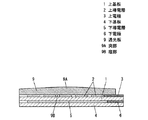
【解決手段】上面中央に上方へ略ドーム状に突出する突部9Aが形成された透光板9の下面に、略半ドーム状に形成された窪部9Bを設けることによって、前後または左右いずれかの方向の透光板9の厚さが均等に形成されると共に、これと直交方向の中央部と外周部の厚さの差も小さくなるため、中央部と外周部を操作した場合の容量変化の誤差を少なくできると共に、透光板9下面への上基板1と下基板4の貼付も容易に行えるため、製作も容易で、確実な操作が可能なタッチパネルを得ることができる。
【選択図】図1
Description
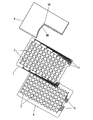
図1は本発明の一実施の形態によるタッチパネルの断面図、図2は同分解斜視図であり、同図において、1はポリエチレンテレフタレートやポリエーテルサルホン、ポリカーボネート等のフィルム状で略矩形状の光透過性の上基板で、上面には酸化インジウム錫や酸化錫等の光透過性で略帯状の複数の上導電層2が、スパッタ法等によって前後方向に配列形成されると共に、一端が上導電層2端部に連結され他端が上基板1の外周右端に延出する、銅や銀、カーボン等の複数の上電極3が形成されている。
2 上導電層
3 上電極
4 下基板
5 下導電層
6 下電極
9 透光板
9A 突部
9B 窪部
Claims (1)
- 上面中央に上方へ略ドーム状に突出する突部が形成された透光板と、上面に所定方向に配列された略帯状で複数の上導電層が形成された上基板と、上面に上記上導電層と直交方向に配列された略帯状で複数の下導電層が形成された下基板からなり、上記下基板上面に上記上基板を、上記上基板上面に上記透光板を重ねて配設すると共に、上記透光板下面に略半ドーム状に形成された窪部を設けたタッチパネル。
Priority Applications (2)
| Application Number | Priority Date | Filing Date | Title |
|---|---|---|---|
| JP2012047631A JP2013182549A (ja) | 2012-03-05 | 2012-03-05 | タッチパネル |
| US13/768,927 US9124275B2 (en) | 2012-03-05 | 2013-02-15 | Touch panel |
Applications Claiming Priority (1)
| Application Number | Priority Date | Filing Date | Title |
|---|---|---|---|
| JP2012047631A JP2013182549A (ja) | 2012-03-05 | 2012-03-05 | タッチパネル |
Publications (2)
| Publication Number | Publication Date |
|---|---|
| JP2013182549A true JP2013182549A (ja) | 2013-09-12 |
| JP2013182549A5 JP2013182549A5 (ja) | 2015-03-12 |
Family
ID=49042198
Family Applications (1)
| Application Number | Title | Priority Date | Filing Date |
|---|---|---|---|
| JP2012047631A Pending JP2013182549A (ja) | 2012-03-05 | 2012-03-05 | タッチパネル |
Country Status (2)
| Country | Link |
|---|---|
| US (1) | US9124275B2 (ja) |
| JP (1) | JP2013182549A (ja) |
Cited By (2)
| Publication number | Priority date | Publication date | Assignee | Title |
|---|---|---|---|---|
| US10838528B2 (en) | 2017-03-14 | 2020-11-17 | Panasonic Intellectual Property Management Co., Ltd. | Touch panel and design structure provided with same |
| US10921940B2 (en) | 2017-03-14 | 2021-02-16 | Panasonic Intellectual Property Management Co., Ltd. | Touch sensor |
Families Citing this family (2)
| Publication number | Priority date | Publication date | Assignee | Title |
|---|---|---|---|---|
| JP2015225570A (ja) * | 2014-05-29 | 2015-12-14 | 富士通テン株式会社 | 操作装置 |
| DE102020121562B4 (de) * | 2020-08-17 | 2023-03-09 | Preh Gmbh | Bedienteil mit verbesserter Befestigung eines Folienschichtaufbaus zur kapazitiven Berührdetektion sowie zugehöriges Montageverfahren |
Citations (2)
| Publication number | Priority date | Publication date | Assignee | Title |
|---|---|---|---|---|
| JP2004265100A (ja) * | 2003-02-28 | 2004-09-24 | Alps Electric Co Ltd | フレキシブルセンサおよびそれを用いた入力装置並びにフレキシブルセンサの製造方法 |
| JP2010128609A (ja) * | 2008-11-25 | 2010-06-10 | Fujitsu Ltd | 表示パネルおよび携帯端末装置 |
Family Cites Families (4)
| Publication number | Priority date | Publication date | Assignee | Title |
|---|---|---|---|---|
| JP2009093397A (ja) | 2007-10-09 | 2009-04-30 | Panasonic Corp | タッチパネル及びこれを用いた入力装置 |
| DE102008049176B4 (de) * | 2008-09-26 | 2011-01-27 | Diehl Ako Stiftung & Co. Kg | Bedienblende für ein Haushaltsgerät sowie Haushaltsgerät mit einer solchen Bedienblende |
| JP2010244336A (ja) | 2009-04-07 | 2010-10-28 | Mitsubishi Electric Corp | タッチセンサ表示装置 |
| TWI457808B (zh) * | 2011-06-09 | 2014-10-21 | Shih Hua Technology Ltd | 觸摸屏 |
-
2012
- 2012-03-05 JP JP2012047631A patent/JP2013182549A/ja active Pending
-
2013
- 2013-02-15 US US13/768,927 patent/US9124275B2/en active Active
Patent Citations (2)
| Publication number | Priority date | Publication date | Assignee | Title |
|---|---|---|---|---|
| JP2004265100A (ja) * | 2003-02-28 | 2004-09-24 | Alps Electric Co Ltd | フレキシブルセンサおよびそれを用いた入力装置並びにフレキシブルセンサの製造方法 |
| JP2010128609A (ja) * | 2008-11-25 | 2010-06-10 | Fujitsu Ltd | 表示パネルおよび携帯端末装置 |
Cited By (2)
| Publication number | Priority date | Publication date | Assignee | Title |
|---|---|---|---|---|
| US10838528B2 (en) | 2017-03-14 | 2020-11-17 | Panasonic Intellectual Property Management Co., Ltd. | Touch panel and design structure provided with same |
| US10921940B2 (en) | 2017-03-14 | 2021-02-16 | Panasonic Intellectual Property Management Co., Ltd. | Touch sensor |
Also Published As
| Publication number | Publication date |
|---|---|
| US20130228441A1 (en) | 2013-09-05 |
| US9124275B2 (en) | 2015-09-01 |
Similar Documents
| Publication | Publication Date | Title |
|---|---|---|
| JP5533364B2 (ja) | タッチパネル | |
| JP2012174003A (ja) | タッチパネル | |
| JP5407599B2 (ja) | タッチパネル | |
| JP2015092422A (ja) | 湾曲型タッチパネル | |
| JP2012048279A (ja) | 入力装置 | |
| US7494358B2 (en) | Touch panel | |
| JP2009277121A (ja) | タッチパネル及びそれを用いた入力装置 | |
| JP6311129B2 (ja) | タッチパネル | |
| JP2007172025A (ja) | タッチパネル | |
| JP2008027016A (ja) | タッチパネル | |
| JP2013182549A (ja) | タッチパネル | |
| JP2011248426A (ja) | タッチパネル | |
| JP2012150580A (ja) | タッチパネル | |
| JP2012003522A (ja) | タッチパネル | |
| JP2014026496A (ja) | タッチパネル | |
| JP2014112356A (ja) | タッチパネル | |
| JP2013050778A (ja) | タッチパネル | |
| JP2012118762A (ja) | タッチパネル | |
| JP2014048675A (ja) | タッチパネル | |
| JP2010257444A (ja) | タッチパネル | |
| JP2014035615A (ja) | タッチパネル | |
| JP2015069609A (ja) | タッチパネル | |
| JP2014170333A (ja) | タッチパネルおよびそれを用いた電子機器 | |
| WO2015083336A1 (ja) | タッチパネル | |
| JP2019003473A (ja) | 操作パネル及び表示装置用ケース |
Legal Events
| Date | Code | Title | Description |
|---|---|---|---|
| A711 | Notification of change in applicant |
Free format text: JAPANESE INTERMEDIATE CODE: A711 Effective date: 20141003 |
|
| A521 | Written amendment |
Free format text: JAPANESE INTERMEDIATE CODE: A523 Effective date: 20150126 |
|
| A621 | Written request for application examination |
Free format text: JAPANESE INTERMEDIATE CODE: A621 Effective date: 20150126 |
|
| A977 | Report on retrieval |
Free format text: JAPANESE INTERMEDIATE CODE: A971007 Effective date: 20151130 |
|
| A131 | Notification of reasons for refusal |
Free format text: JAPANESE INTERMEDIATE CODE: A131 Effective date: 20151208 |
|
| A02 | Decision of refusal |
Free format text: JAPANESE INTERMEDIATE CODE: A02 Effective date: 20160405 |