JP2013161992A - Deformable reflective optical element, optical system, and exposure device - Google Patents
Deformable reflective optical element, optical system, and exposure device Download PDFInfo
- Publication number
- JP2013161992A JP2013161992A JP2012023554A JP2012023554A JP2013161992A JP 2013161992 A JP2013161992 A JP 2013161992A JP 2012023554 A JP2012023554 A JP 2012023554A JP 2012023554 A JP2012023554 A JP 2012023554A JP 2013161992 A JP2013161992 A JP 2013161992A
- Authority
- JP
- Japan
- Prior art keywords
- optical system
- back surface
- reflective
- deformable
- optical element
- Prior art date
- Legal status (The legal status is an assumption and is not a legal conclusion. Google has not performed a legal analysis and makes no representation as to the accuracy of the status listed.)
- Pending
Links
Images


Landscapes
- Exposure And Positioning Against Photoresist Photosensitive Materials (AREA)
- Exposure Of Semiconductors, Excluding Electron Or Ion Beam Exposure (AREA)
- Optical Elements Other Than Lenses (AREA)
Abstract
Description
本発明は、変形可能な反射光学素子、この反射光学素子を有する光学系、及びこの光学系を備える露光装置に関する。さらに本発明は、露光装置を用いるデバイス製造方法に関する。 The present invention relates to a deformable reflective optical element, an optical system having the reflective optical element, and an exposure apparatus including the optical system. Furthermore, the present invention relates to a device manufacturing method using an exposure apparatus.
例えば半導体デバイスの製造工程の一つであるリソグラフィ工程においては、レチクル(又はフォトマスク等)に形成されているパターン、又は空間光変調器等で生成されるパターンを、投影光学系を介してフォトレジストが塗布されたウエハ(又はガラスプレート等)の表面に転写するために、ステッパー等の一括露光型の露光装置、又はスキャニングステッパー等の走査露光型等の露光装置等が使用されている。 For example, in a lithography process, which is one of the manufacturing processes of a semiconductor device, a pattern formed on a reticle (or a photomask or the like) or a pattern generated by a spatial light modulator or the like is photo-transmitted via a projection optical system. A batch exposure type exposure apparatus such as a stepper or a scanning exposure type exposure apparatus such as a scanning stepper is used to transfer the resist onto the surface of a wafer (or glass plate or the like) coated with a resist.
これらの露光装置に搭載される投影光学系は、諸収差が所定の許容範囲内に収まるように組立調整が行われる。この際に、例えば歪曲収差や倍率誤差等の回転対称で、かつ低次数の収差成分が残存していても、これらの収差は投影光学系に装着されている通常の結像特性補正機構(例えば所定のレンズ及び/又はミラーの光軸方向の位置や傾斜角を制御する機構)によって補正することができる。これに対して、光軸上での非点収差(以下、センターアスと言う。)のような非回転対称な収差成分が残存している場合には、従来の通常の結像特性補正機構ではその補正は困難である。 The projection optical system mounted on these exposure apparatuses is assembled and adjusted so that various aberrations are within a predetermined allowable range. At this time, for example, even if rotational aberrations such as distortion aberration and magnification error and low-order aberration components remain, these aberrations are not affected by normal imaging characteristic correction mechanisms (for example, mounted on the projection optical system) This can be corrected by a mechanism that controls the position and tilt angle of the predetermined lens and / or mirror in the optical axis direction. On the other hand, when a non-rotationally symmetric aberration component such as astigmatism on the optical axis (hereinafter referred to as “center astigmatism”) remains, The correction is difficult.
そこで、そのような非回転対称な収差成分を補正するために、投影光学系が備えるミラーの側面の凸部をアクチュエータで微小量変形させることによって、そのミラーの反射面の形状を変形させるようにした補正機構が提案されている(例えば、特許文献1参照)。この補正機構によれば、比較的小さい力でその反射面を変形させることができる。 Therefore, in order to correct such a non-rotationally symmetric aberration component, the projection on the side surface of the mirror included in the projection optical system is deformed by a small amount by an actuator so that the shape of the reflecting surface of the mirror is deformed. A correction mechanism has been proposed (see, for example, Patent Document 1). According to this correction mechanism, the reflecting surface can be deformed with a relatively small force.
従来の非回転対称な収差成分の補正機構は、ミラー側面の凸部を機械的に変形させていたため、その凸部の変形量とミラーの反射面の変形量との関係が複雑で、その反射面を目標とする形状に高精度に変形させるのが困難であるとともに、その反射面を種々の複雑な形状に変形させるのが困難であった。
また、従来の補正機構は、ミラー側面の凸部に反射面側に向かう正の最大荷重と反射面の裏面側に向かう負の最大荷重との間で、可変の荷重を付与する機構であったため、補正機構が複雑であった。
The conventional non-rotationally symmetric aberration component correction mechanism mechanically deforms the convex part on the side of the mirror, so the relationship between the deformation amount of the convex part and the deformation amount of the reflecting surface of the mirror is complicated, and its reflection It is difficult to deform the surface into a target shape with high accuracy, and it is difficult to deform the reflecting surface into various complicated shapes.
In addition, the conventional correction mechanism is a mechanism that applies a variable load between the positive maximum load toward the reflecting surface side and the negative maximum load toward the back surface side of the reflecting surface on the convex portion of the mirror side surface. The correction mechanism was complicated.
本発明の態様は、このような事情に鑑み、簡単な機構を用いて反射部材の反射面を種々の形状に容易に変形可能とすることを目的とする。 In view of such circumstances, it is an object of an aspect of the present invention to easily change the reflecting surface of a reflecting member into various shapes using a simple mechanism.
本発明の第1の態様によれば、光を反射する変形可能な反射光学素子が提供される。この反射光学素子は、光を反射する反射面を有する反射部材と、その反射部材の周辺部を保持する保持部と、その反射部材のその反射面の裏面に対して所定方向の力を与えて、前記所定方向に関する第1位置と第2位置との間で、前記反射面を変形させる少なくとも一つの駆動部と、を備え、その駆動部からその裏面に対してその所定方向の力が付与されていないとき、その反射面は、その第2位置にあるものである。 According to the first aspect of the present invention, a deformable reflective optical element that reflects light is provided. The reflective optical element applies a force in a predetermined direction to a reflective member having a reflective surface that reflects light, a holding unit that holds the periphery of the reflective member, and the back surface of the reflective surface of the reflective member. And at least one driving unit that deforms the reflecting surface between a first position and a second position with respect to the predetermined direction, and a force in the predetermined direction is applied from the driving unit to the back surface. When not, the reflective surface is in its second position.
また、第2の態様によれば、複数の光学素子を含む光学系が提供される。この光学系は、第1の態様の変形可能な反射光学素子を備え、その光学系の非回転対称な収差に応じてその駆動部を介してその反射光学素子のその反射部材のその反射面の変形量が制御されるものである。
また、第3の態様によれば、露光光でパターンを照明し、その露光光でそのパターン及び投影光学系を介して基板を露光する露光装置において、第2の態様の光学系を備える露光装置が提供される。
According to the second aspect, an optical system including a plurality of optical elements is provided. The optical system includes the deformable reflective optical element according to the first aspect, and the reflection surface of the reflective member of the reflective optical element via the drive unit according to the non-rotationally symmetric aberration of the optical system. The amount of deformation is controlled.
Further, according to the third aspect, in the exposure apparatus that illuminates the pattern with the exposure light and exposes the substrate with the exposure light through the pattern and the projection optical system, the exposure apparatus including the optical system of the second aspect Is provided.
また、第4の態様によれば、第3の態様の露光装置を用いて基板上に感光層のパターンを形成することと、そのパターンが形成されたその基板を処理することと、を含むデバイス製造方法が提供される。 According to the fourth aspect, a device comprising: forming a pattern of a photosensitive layer on a substrate using the exposure apparatus of the third aspect; and processing the substrate on which the pattern is formed A manufacturing method is provided.
本発明の態様によれば、駆動部から反射部材の反射面の裏面に対して与える所定方向の力を変化させることで、その反射面をその第1位置と第2位置との間で変形させることができる。従って、簡単な機構を用いてその反射面を種々の形状に容易に変形可能である。 According to the aspect of the present invention, the reflective surface is deformed between the first position and the second position by changing the force in a predetermined direction applied from the drive unit to the back surface of the reflective surface of the reflective member. be able to. Therefore, the reflecting surface can be easily deformed into various shapes using a simple mechanism.
以下、本発明の実施形態の一例につき図1〜図6を参照して説明する。
図1は、本実施形態の露光装置EXの露光本体部を示す。露光装置EXは、一例としてスキャニングステッパー(スキャナー)よりなる走査露光型の投影露光装置である。図1において、露光装置EXは、露光用の照明光IL(露光光)を発生する露光光源(不図示)と、照明光ILでレチクルR(マスク)を照明する照明光学系ILS(図1ではこの一部のみが表れている)と、レチクルRのパターンの像をウエハW(基板)の表面に形成する投影光学系PLとを備えている。さらに、露光装置EXは、レチクルRを保持して移動するレチクルステージ15と、ウエハWを保持して移動するウエハステージ32と、装置全体の動作を統括的に制御するコンピュータよりなる主制御系5(図2参照)とを備えている。
Hereinafter, an exemplary embodiment of the present invention will be described with reference to FIGS.
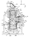
FIG. 1 shows an exposure main body of the exposure apparatus EX of the present embodiment. The exposure apparatus EX is, for example, a scanning exposure type projection exposure apparatus composed of a scanning stepper (scanner). In FIG. 1, an exposure apparatus EX includes an exposure light source (not shown) that generates exposure illumination light IL (exposure light) and an illumination optical system ILS that illuminates a reticle R (mask) with the illumination light IL (in FIG. 1). And a projection optical system PL that forms an image of the pattern of the reticle R on the surface of the wafer W (substrate). Further, the exposure apparatus EX includes a
以下、投影光学系PLのレチクルR側の部分光学系(後述の第1結像光学系G1)の光軸AX1に平行にZ軸を取り、Z軸に垂直な平面(本実施形態ではほぼ水平面)内で図1の紙面に平行にY軸を、図1の紙面に垂直にX軸を取って説明する。走査露光時のレチクルR及びウエハWの走査方向はY軸に平行な方向(Y方向)であり、レチクルRのパターン面及びウエハWの表面はXY面にほぼ平行である。また、X軸、Y軸、及びZ軸に平行な軸の回りの回転方向(傾斜方向)をθx方向、θy方向、及びθz方向とも呼ぶ。 Hereinafter, a plane that takes the Z axis parallel to the optical axis AX1 of the partial optical system on the reticle R side of the projection optical system PL (first imaging optical system G1 described later) and is perpendicular to the Z axis (in the present embodiment, substantially horizontal) ), The Y axis is parallel to the paper surface of FIG. 1, and the X axis is perpendicular to the paper surface of FIG. The scanning direction of reticle R and wafer W during scanning exposure is a direction (Y direction) parallel to the Y axis, and the pattern surface of reticle R and the surface of wafer W are substantially parallel to the XY plane. The rotation directions (inclination directions) around the axes parallel to the X axis, the Y axis, and the Z axis are also referred to as the θx direction, the θy direction, and the θz direction.
まず、投影光学系PL、レチクルステージ15、及びウエハステージ32を含む露光本体部は、フレーム機構によって支持されている。そのフレーム機構は、床面に設置されたフレームキャスタよりなるベース部材1と、ベース部材1の上面に設置された例えば3本(4本等でも可)の第1コラム2と、これらの第1コラム2の上面に例えば能動型の防振装置3A,3B(実際には3個又は4個配置されている)を介して設置された第2コラム4とを備えている。第2コラム4の底部に設けられた平板状の支持板部4aの中央のU字型の開口部に投影光学系PLが搭載されている。
First, the exposure main body including the projection optical system PL, the
そのフレーム機構の近傍に設置された露光光源(不図示)は、ArFエキシマレーザ光源(発振波長193nm)であるが、その他にKrFエキシマレーザ光源(波長248nm)、又は固体レーザ(YAGレーザ若しくは半導体レーザ等)の高調波発生装置等も使用できる。その露光光源から射出された照明光ILは、照明光学系ILSに入射する。照明光学系ILSは、レチクルRのパターン面(下面)のX方向(非走査方向)に細長いスリット状の照明領域を照明光ILによりほぼ均一な照度分布で照明する。 An exposure light source (not shown) installed in the vicinity of the frame mechanism is an ArF excimer laser light source (oscillation wavelength 193 nm). In addition, a KrF excimer laser light source (wavelength 248 nm), or a solid-state laser (YAG laser or semiconductor laser) Etc.) can be used. The illumination light IL emitted from the exposure light source enters the illumination optical system ILS. The illumination optical system ILS illuminates a slit-like illumination area elongated in the X direction (non-scanning direction) of the pattern surface (lower surface) of the reticle R with illumination light IL with a substantially uniform illuminance distribution.
サブチャンバ14内に配置された照明光学系ILSは、例えば米国特許出願公開第2003/025890号明細書などに開示されるように、空間光変調器又は回折光学素子等を含む光量分布設定機構(不図示)、オプティカルインテグレータ(フライアイレンズ又はロッドインテグレータなど)等を含む照度均一化光学系(不図示)、レチクルブラインド等の可変視野絞り(不図示)、並びにレンズ11,13及びミラー12を含むコンデンサ光学系等を含んでいる。また、通常照明、2極照明、4極照明、又は輪帯照明等の照明条件に応じて、その光量分布設定機構が、照明光学系ILS内の瞳面(不図示)における照明光ILの光量分布を、光軸を中心とする円形領域、光軸を挟む2つの領域、光軸を挟む4つの領域、又は輪帯状の領域等でそれぞれ大きい光量となる分布に切り換える。
The illumination optical system ILS disposed in the
レチクルRを通過した照明光ILは、投影光学系PLを介して、フォトレジスト(感光剤)が塗布された円板状の基板であるウエハ(半導体ウエハ)Wの表面の一つのショット領域のX方向に細長い露光領域に、レチクルRの照明領域内のパターンを投影倍率β(例えば1/4,1/5等)で縮小した像を形成する。本実施形態の投影光学系PLは反射屈折光学系である。投影光学系PLは、フランジ部44aによって架台4aに載置されている。照明光学系ILS及び投影光学系PLの照明光ILの光路はほぼ気密化され、これらの光路には、ほぼ真空紫外域の光に対して高透過率の気体(以下、「パージガス」と呼ぶ)であるドライエアー、窒素、又は希ガス(ヘリウム等)等が、供給用の配管20A等及び排気用の配管21A,21D等を介して供給されている。
The illumination light IL that has passed through the reticle R passes through the projection optical system PL, and the X of one shot region on the surface of a wafer (semiconductor wafer) W that is a disk-shaped substrate coated with a photoresist (photosensitive agent). An image obtained by reducing the pattern in the illumination area of the reticle R with a projection magnification β (for example, 1/4, 1/5, etc.) is formed in the exposure area that is elongated in the direction. The projection optical system PL of the present embodiment is a catadioptric optical system. The projection optical system PL is placed on the
また、レチクルRは、レチクルホルダ(不図示)を介してレチクルステージ15の上面に保持され、レチクルステージ15はレチクルベース16のXY面に平行な上面に、Y方向に一定速度で移動可能に、かつX方向、Y方向、θz方向に変位可能な状態で載置されている。レチクルベース16は、第2コラム4の上端に固定されている。レチクルステージ15の少なくともX方向、Y方向の位置、及びθz方向の回転角はレーザ干渉計17によって計測され、この計測値及び主制御系5からの制御情報に基いて、リニアモータ等を含む駆動装置(不図示)がレチクルステージ15を駆動する。
The reticle R is held on the upper surface of the
一方、ウエハWは、ウエハホルダ(不図示)を介してウエハテーブル31の上面に保持され、ウエハテーブル31はウエハステージ32の上面に固定されている。ウエハステージ32は、ウエハベース33のXY面に平行な上面にY方向に一定速度で移動可能に、かつX方向、Y方向にステップ移動可能に載置されている。ウエハベース33は、能動型の防振装置38A,38B等を介してベース部材1上に載置されている。ウエハステージ32の少なくともX方向、Y方向の位置、及びθz方向の回転角はレーザ干渉計34(又はエンコーダ装置等)によって計測され、この計測値及び主制御系5からの制御情報に基いて、リニアモータ等を含む駆動装置(不図示)がウエハステージ32を駆動する。
On the other hand, the wafer W is held on the upper surface of the wafer table 31 via a wafer holder (not shown), and the wafer table 31 is fixed to the upper surface of the
また、ウエハステージ32の内部には、ウエハテーブル31(ウエハW)のZ方向の位置(フォーカス位置)と、θx方向及びθy方向の傾斜角とを調整するためのフォーカス・レベリング機構が組み込まれている。投影光学系PLの下部側面に配置された投射光学系35Aと受光光学系35Bとから構成される斜入射方式の多点の焦点位置検出系(オートフォーカスセンサ)によって計測されるウエハWの複数の計測点でのフォーカス位置の情報に基いて、そのフォーカス・レベリング機構は、露光中に継続してウエハWの表面を投影光学系PLの像面に合焦させる。投射光学系35A及び受光光学系35Bは、投影光学系PLのフランジ部44aの底面に取り付けられたセンサーコラム36に取り付けられている。
In addition, a focus / leveling mechanism for adjusting the Z-direction position (focus position) of the wafer table 31 (wafer W) and the inclination angles in the θx direction and the θy direction is incorporated in the
また、ウエハテーブル31の上部に、例えば米国特許第6,573,997号明細書等で開示されているシアリング干渉方式又はポイント・ディフラクション・干渉方式(PDI方式)の波面収差計測装置39が設けられている。波面収差計測装置39によって計測される投影光学系PLの波面収差の情報は図2の結像特性制御系6に供給される。結像特性制御系6では、通常の露光時には、例えば照明光ILの積算エネルギー等に基づいて、投影光学系PLの波面収差の変動量を逐次予測している。
In addition, a shearing interference type or point / diffraction / interference type (PDI type) wavefront
露光時には、不図示のアライメント系を用いてレチクルR及びウエハWのアライメントを行った後、ウエハステージ32をX方向、Y方向にステップ移動することで、ウエハWの露光対象のショット領域が露光領域の手前に移動する。その後、レチクルRの照明領域内のパターンの投影光学系PLによる像でウエハWの当該ショット領域を露光しつつ、レチクルステージ15及びウエハステージ32を介してレチクルRとウエハWとをY方向に投影光学系PLの投影倍率を速度比として同期移動する走査露光が行われる。そのステップ移動と走査露光とをステップ・アンド・スキャン方式で繰り返すことによって、ウエハWの全部のショット領域にレチクルRのパターンの像が露光される。
At the time of exposure, after aligning the reticle R and the wafer W using an alignment system (not shown), the
次に、本実施形態の投影光学系PLの構成等につき詳細に説明する。図1において、反射屈折光学系からなる投影光学系PLは、レチクルRのパターンの第1中間像を形成する屈折型の第1結像光学系G1と、凹面鏡よりなるミラー要素22と2つの負屈折力のレンズL8,L9とから構成されて第1中間像とほぼ等倍の第2中間像を形成する第2結像光学系G2と、第2中間像からの光を用いてウエハW上にレチクルRのパターンの最終像を形成する屈折型の第3結像光学系G3と、デフォーマブルミラー50と、を備えている。デフォーマブルミラー50は、ミラー要素22を含み、ミラー要素22の反射面の形状を制御可能である。さらに、投影光学系PLは、第1結像光学系G1からの光を第2結像光学系G2に向かって偏向する反射面Aと、第2結像光学系G2からの光を第3結像光学系G3に向かって偏向する反射面Bとが形成された光路折り曲げ鏡FMを備えている。第1中間像及び第2中間像は、それぞれほぼ反射面Aと第1結像光学系G1との間、及び反射面Bと第3結像光学系G3との間に形成される。
Next, the configuration of the projection optical system PL of the present embodiment will be described in detail. In FIG. 1, a projection optical system PL composed of a catadioptric optical system includes a refractive first imaging optical system G1 that forms a first intermediate image of a reticle R pattern, a
また、第1結像光学系G1及び第3結像光学系G3はZ軸に平行な光軸AX1を有し、第2結像光学系G2の光軸AX2は、光軸AX1と直交するように、かつY軸に平行に設定されている。更に、光路折り曲げ鏡FMの2つの反射面A,Bの交線(厳密にはその仮想延長面の交線)Cで光軸AX1と光軸AX2とが交差している。
第1結像光学系G1は、レチクルR側から順に、平行平面板L1、レンズL2,L3,L4,L5,L6,L7を配置して構成されている。第2結像光学系G2は、光の進行往路に沿ってレチクル側(即ち入射側)から順に、負のレンズL8及びL9と、ミラー要素22とを配置して構成されている。第3結像光学系G3は、光の進行方向に沿ってレチクル側から順に、レンズL10,L11と、開口絞りASと、レンズL12,L13とを配置して構成されている。開口絞りASの配置面は投影光学系PLの瞳面又はその近傍の面であり、ミラー要素22の反射面22dは、投影光学系PLの瞳面とほぼ共役である。なお、投影光学系PLの構成は任意である。
The first imaging optical system G1 and the third imaging optical system G3 have an optical axis AX1 parallel to the Z axis, and the optical axis AX2 of the second imaging optical system G2 is orthogonal to the optical axis AX1. And parallel to the Y axis. Further, the optical axis AX1 and the optical axis AX2 intersect at an intersection line C (strictly speaking, an intersection line of the virtual extension surfaces) C of the two reflection surfaces A and B of the optical path bending mirror FM.
The first imaging optical system G1 includes a plane parallel plate L1, lenses L2, L3, L4, L5, L6, and L7 arranged in this order from the reticle R side. The second imaging optical system G2 is configured by arranging negative lenses L8 and L9 and a
本実施形態において、投影光学系PLを構成する全ての屈折光学素子(レンズ成分)の光学材料には合成石英又は蛍石(CaF2 結晶)を使用している。また、光路折り曲げ鏡FM及びミラー要素22は、一例としてコーニング社のULE(Ultra Low Expansion:商品名)などの超低膨張率のガラス材料、又はショット社のゼロデュア(Zerodur:商品名)などの低膨張率のガラスセラミックス材料から形成できる。例えばULEを用いる場合のミラー要素22のヤング率(ほぼ67.6GPa)は鉄鋼の1/3程度であり、ポアソン比(ほぼ0.17)は鉄鋼の1/2程度であり、ミラー要素22では同じ荷重(応力)に対して鉄鋼の3倍程度の弾性変形がある。これらの材料の反射面はアルミニウム等の金属膜又は誘電体多層膜を被着することにより形成される。また、ミラー要素22の材料としてベリリウム(Be)等の金属を用いても良い。ベリリウムを用いる場合には、ミラー要素22全体を炭化ケイ素等でコーティングすることが好ましい。
In this embodiment, synthetic quartz or fluorite (CaF 2 crystal) is used as the optical material of all refractive optical elements (lens components) constituting the projection optical system PL. The optical path bending mirror FM and the
また、第1結像光学系G1の平行平面板L1、レンズL2〜L7は、それぞれ輪帯状のレンズ枠42A,42B,42C,42D,42E,42F,42Gを介して円筒状の分割鏡筒41A,41B,41C,41D,41E,41F,41G内に保持され、分割鏡筒41A〜41Gは光軸AX1に沿って気密性を保持する状態で例えば対向するフランジ部(不図示)をボルト(不図示)で固定して連結されている。レンズ枠42B〜42G等には上記のパージガスを流通させるための複数の開口が形成されている(以下同様)。
In addition, the plane parallel plate L1 and the lenses L2 to L7 of the first imaging optical system G1 are respectively divided into cylindrical divided
同様に、第3結像光学系G3のレンズL10,L11,L12,L13は、それぞれ輪帯状のレンズ枠42H,42K,42I,42Jを介して円筒状の分割鏡筒41H,44,41I,41J内に保持されている。開口絞りASは、分割鏡筒44,41Iに挟まれた分割鏡筒41K内に保持され、分割鏡筒41H,44,41K,41I,41Jは気密性を保持する状態で連結されている。そして、分割鏡筒44にフランジ部44aが設けられている。分割鏡筒41G,41H間に+Y方向に開口が設けられた円筒状の分割鏡筒43が連結され、分割鏡筒43内の突部に保持枠43aを介して光路折り曲げ鏡FMが固定されている。分割鏡筒41A〜41K,43,44より第1の部分鏡筒7が構成されている。
Similarly, the lenses L10, L11, L12, and L13 of the third imaging optical system G3 are respectively divided into cylindrical divided lens barrels 41H, 44, 41I, and 41J via annular lens frames 42H, 42K, 42I, and 42J. Is held in. The aperture stop AS is held in the divided
また、図2の結像特性制御系6の制御のもとで、例えばレンズ枠42A〜42Eを駆動して、平行平面板L1、レンズL2〜L5をZ方向、θx方向、θy方向に微動することによって、投影光学系PLのディストーション及びコマ収差等の回転対称で比較的低次の収差を補正する回転対称な結像特性補正機構(不図示)が設けられている。このような回転対称な結像特性補正機構としては、例えば米国特許出願公開第2006/244940号明細書に開示されている機構を使用可能である。
Further, under the control of the imaging
また、第2結像光学系G2のレンズL8,L9は、それぞれ保持枠46A,46Bを介して、円筒型の分割鏡筒45,41L内に保持され、ミラー要素22を含むデフォーマブルミラー50は、分割鏡筒41Lに連結されて保持されている。デフォーマブルミラー50は、投影光学系PLの結像特性としてのセンターアス等の非回転対称な収差及び高次の収差を含む波面収差を補正するための補正機構でもある。本実施形態では、その波面収差をツェルニケ(Zernike)多項式の係数(以下、ツェルニケ係数ziという)で表すものとする。図2の結像特性制御系6は、通常の露光時には、予測される投影光学系PLの結像特性の変動量のうち、回転対称で比較的低次の収差を除く波面収差(例えば5次〜81次のツェルニケ係数ziで表される収差)の情報を図2の収差制御系9に供給する。収差制御系9では、その波面収差を補正するようにデフォーマブルミラー50のミラー要素22の反射面22dを変形させる。収差制御系9には、デフォーマブルミラー50を駆動するための情報が記憶された記憶装置10が連結されている。
The lenses L8 and L9 of the second imaging optical system G2 are held in the cylindrical divided lens barrels 45 and 41L via the holding frames 46A and 46B, respectively, and the
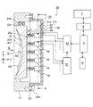
デフォーマブルミラー50は、ミラー要素22がホールドブロック23を介して収納された円筒状の分割鏡筒47と、分割鏡筒47の+Y方向の開口を覆うように分割鏡筒47の端面47bに固定されたハウジング53と、ハウジング53の内面に設けられてミラー要素22の反射面22dを変形させる荷重付与系54と、を備えている。なお、分割鏡筒47は、分割鏡筒41Lに連結される。
The
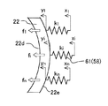
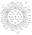
図2に示すように、荷重付与系54は、ミラー要素22の裏面22eの複数の作用点Pi(i=1〜n;nは2以上の整数)に裏面22eから反射面22dの方向(−Y方向)に向かう可変の荷重fi(fi≧0)を付与する複数の駆動ユニット58を有する。複数の駆動ユニット58は、互いに同じ構成である。複数の駆動ユニット58の+Y方向の端部はハウジング53の内面に固定され、ハウジング53は複数のボルト40Aを介して分割鏡筒47に固定されている。複数の駆動ユニット58の−Y方向の端部はミラー要素22の裏面22eに離脱可能な状態で接触している。また、図2のAA線に沿う断面図である図3に示すように、外形がほぼ円柱状のミラー要素22の側面に、等角度間隔で3箇所の凸形状の保持部22a,22b,22cが形成されている。保持部22a,22b,22cのそれぞれは、ホールドブロック23A,23B,23Cに保持されており、ホールドブロック23A,23B,23Cは、分割鏡筒47の内面に固定されている。ミラー要素22は、3つのホールドブロック23A〜23Cによってキネマティックに安定に支持されている。なお、ホールドブロック23A〜23Cは、図1では代表的に一つのホールドブロック23で表されている。
As shown in FIG. 2, the
また、一例として、荷重付与系54の複数の駆動ユニット58は、ミラー要素22の裏面22eにほぼ均等に格子状に配置された複数の作用点Pi(図3では19個の作用点P1〜P19)に荷重を付与するように配置されている。一例として、中央の作用点P10は、光軸AX2上に位置している。なお、例えば中央の作用点P10の代わりに、Z方向に離れて配置された2つの作用点を用いることによって、作用点Pi(駆動ユニット58)を偶数(例えば20個)とすることもできる。なお、作用点Pi(駆動ユニット58)の個数及び配置は任意である。
Further, as an example, the plurality of
図2において、作用点Piに荷重を与える駆動ユニット58は、ハウジング53の内面に一端が固定されたロードセル等の荷重センサ60と、荷重センサ60の他端に固定されてY方向に伸縮可能な駆動素子59と、駆動素子59の先端部に一端が固定された圧縮ばね61とを有する。例えば、この圧縮ばね61は、剛性の高い、例えば鉄鋼又はステンレス等の金属製の圧縮コイルばねで形成してもよい。圧縮ばね61の他端には、ミラー要素22の裏面22eの作用点Piに接触する半球状の金属製の接触部61aが設けられている。なお、接触部61aとしては、平面部で裏面22eに接触する部材を使用してもよい。また、駆動素子59としては、ピエゾ素子又は超音波モータ等が使用できる。
In FIG. 2, the
荷重センサ60は、駆動ユニット58によってハウジング53からミラー要素22の裏面22eに向けて−Y方向に付与される荷重の情報を含む検出信号を検出信号処理系57に供給する。検出信号処理系57では、荷重センサ60の検出信号から各作用点Piの荷重を求め、このようにして求めた荷重の情報を駆動素子制御系56に供給する。駆動素子制御系56では、各作用点Piの荷重が収差制御系9に設定される目標値になるように対応する駆動ユニット58の駆動素子59の伸縮量を制御する。
The
収差制御系9は、結像特性制御系6から供給される補正対象の波面収差(ミラー要素22の反射面22dのn個の位置での目標変形量の情報)及び記憶装置10に記憶されているミラー要素22のヤング率及びポアソン比(弾性係数)の情報から、反射面22dに対応する裏面22eの作用点Piにおける−Y方向への荷重の目標値を計算する。収差制御系9は、計算した荷重の目標値の情報を駆動素子制御系56に供給する。これによって、反射面22dの形状は例えば理想面BDを含む変形可能範囲内の任意の面B2の近傍に設定可能である。この場合、全体としてのミラー要素22の反射面の変形の自由度はnであり、各自由度で変形可能範囲の任意の変形量を設定できる。
The
なお、本実施形態の理想面BDとは、図1の第1及び第3結像光学系G1,G3及び第2結像光学系G2(ここではミラー要素22を除く部分)が実質的に無収差である場合に、投影光学系PLを実質的に無収差とするために必要なミラー要素22の反射面22dの面形状を表している。また、本実施形態では、反射面22dの変形可能範囲はその理想面BDを中心としているため、理想面BDは中立面でもある。本実施形態においてその変形可能範囲とは、例えば照明光ILの照射エネルギーの積算値によって投影光学系PLの結像特性が変化するときに、経験的又は計算上でその結像特性の変化を補正(相殺)するために必要なミラー要素22の反射面22dの形状の弾性変形による可変範囲を含むものである。
Note that the ideal plane BD of the present embodiment is substantially free of the first and third imaging optical systems G1, G3 and the second imaging optical system G2 (here, the portion excluding the mirror element 22) in FIG. In the case of aberration, the surface shape of the reflecting
本実施形態では、図4(C)に示すように、全部の駆動ユニット58からミラー要素22の裏面22eに対して−Y方向への荷重fiが付与されていない状態(全部のfi=0の状態)では、ミラー要素22の反射面22dが、変形可能範囲で最も裏面22eに近い方向の位置にある下限面B1に合致するように、予めミラー要素22の反射面22dは理想面BDに対応して凹面に形成されている。本実施形態では、下限面B1の形状は非球面である。すなわち、ミラー要素22は、反射面22dが理想面BDに対して、凹んだ状態の非球面加工が施されている。
In the present embodiment, as shown in FIG. 4 (C), a state where a load f i is not added from the whole of the
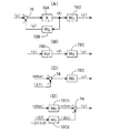
そして、例えば露光を開始した直後で、投影光学系PLの結像特性が目標とする状態からほとんど変化していない状態では、図4(A)に示すように、荷重付与系54の全部の駆動ユニット58においてミラー要素22の裏面22eに対して−Y方向に向かう荷重fiをそれぞれ可変範囲内の中央の値Si/2に設定する。これによって、ミラー要素22の反射面22dはほぼ理想面BDに合致するように弾性変形するため、投影光学系PLの結像特性は目標とする状態に維持される。
Then, for example, immediately after the start of exposure, when the imaging characteristics of the projection optical system PL have hardly changed from the target state, as shown in FIG. In the
その後、露光継続中に、照明光ILの照射エネルギーの積算によって投影光学系PLの結像特性が大きく変化して、例えば波面収差が光軸付近で正の最大値になるように均一に増大した状態では、図4(B)に示すように、荷重付与系54の全部の駆動ユニット58において裏面22eに対して−Y方向に向かう荷重fiをそれぞれ可変範囲内の最大値Siに設定する。これに対応して、ミラー要素22の反射面22dは弾性変形によって変形可能範囲内で最も裏面22eから離れた方向の位置にある上限面B3の近傍に変形し、ミラー要素22における波面収差が負になるため、投影光学系PLの結像特性は目標とする状態に維持される。
Thereafter, during the exposure continuation, the imaging characteristics of the projection optical system PL changed greatly due to the integration of the irradiation energy of the illumination light IL, and for example, the wavefront aberration increased uniformly so as to become a positive maximum value near the optical axis. In the state, as shown in FIG. 4B, in all the
一方、例えば波面収差が光軸付近で負の最大値になるように均一に減少した状態では、図4(C)に示すように、荷重付与系54の全部の駆動ユニット58において裏面22eに対して−Y方向に向かう荷重fiをそれぞれ可変範囲内の最小値(=0)付近に設定する。これに対応して、ミラー要素22の反射面22dは、弾性変形の復元力によって変形可能範囲内で最も裏面22eに近い下限面B1の近傍の形状に戻り、ミラー要素22における波面収差が正になるため、投影光学系PLの結像特性は目標とする状態に維持される。そして、荷重付与系54の全部の駆動ユニット58から裏面22eに付与する−Y方向の荷重を独立に制御することによって、ミラー要素22の反射面22dの形状を下限面B1と上限面B3との間の任意の面B2の近傍に設定することができ、これによって常に投影光学系PLの結像特性を目標とする状態に維持できる。
On the other hand, for example, in a state where the wavefront aberration is uniformly reduced so as to have a negative maximum value in the vicinity of the optical axis, as shown in FIG. respectively set to the minimum value (= 0) near the variable range of load f i toward the -Y direction Te. Correspondingly, the reflecting
ここで、予めミラー要素22の反射面22dの形状を変形可能範囲内の下限面B1に形成しておくことにより、複数の駆動ユニット58から裏面22eに−Y方向に可変の荷重を与えることで、反射面22dを下限面B1以上の任意の形状に弾性変形できることにつき、図5〜図6(D)を参照して説明する。まず、図2のミラー要素22及び複数の駆動ユニット58を図5に示すように簡略化して示す。図5において、ミラー要素22のi番目(i=1〜n)の作用点に関して、駆動ユニット58の圧縮コイルばね61のばね定数をki、圧縮コイルばね61の入力変位をxi、圧縮コイルばね61による裏面22e(作用点)の変位をyi、駆動ユニット58による裏面22eに対する荷重をfiとする。また、このときに各作用点に対応するミラー要素22の反射面22dの各点における−Y方向への変形量の分布をツェルニケ係数ziを用いて表すものとすると、反射面22dの面変形量は次のm個のツェルニケ係数zi(i=1〜m)のベクトル<z>で表すことができる。なお、例えばツェルニケ係数z1〜z81を使用する場合には、m=81である。
Here, by previously forming the shape of the

<f>=K(<x>−<y>) …(12)
また、裏面22eの荷重のベクトル<f>と、作用点の変位のベクトル<y>及び反射面22dの変形量の分布を表すツェルニケ係数のベクトル<z>との関係を、n行×n列の行列Rfy及びm行×n列の行列Rfzを用いて次のように表す。行列Rfzにおいて行数を表すmは使用するツェルニケ係数の項数を表しており、例えばm=81である。
<F> = K (<x> − <y>) (12)
Also, the relationship between the load vector <f> on the
<y>=Rfy<f> …(13A), <z>=Rfz<f> …(13B)
式(12)、式(13A)、及び式(13B)の関係は、図5に対応する図6(A)のブロック図で表すことができる。図6(A)において、減算部70からの差分(<x>−<y>)に乗算部72Aで行列Kが乗算されて荷重のベクトル<f>が求められ、ベクトル<f>には乗算部72B及び72Cでそれぞれ行列Rfy及びRfzが乗算される。
<Y> = Rfy <f> (13A), <z> = Rfz <f> (13B)
The relationship between Expression (12), Expression (13A), and Expression (13B) can be expressed by the block diagram of FIG. 6A corresponding to FIG. In FIG. 6A, the difference (<x> − <y>) from the
図6(A)から次の関係が得られる。
<f>=K<x>−K・Rfy<f> …(14A)
この式を変形すると次のようになる。
K<x>=(En+K・Rfy)<f> …(14B)
なお、式(14B)中のn行×n列の行列Enは単位行列である。そして、式(14B)を変形すると次式が得られる。
The following relationship is obtained from FIG.
<F> = K <x> −K · Rfy <f> (14A)
This equation is transformed as follows.
K <x> = (En + K · Rfy) <f> (14B)
Note that the matrix En of n rows × n columns in the equation (14B) is a unit matrix. When the equation (14B) is modified, the following equation is obtained.
<f>=(En−K・Rfy)-1K<x>=Rxf<x> …(15A)
ただし、Rxf=(En−K・Rfy)-1 …(15B)
式(15A)を用いると、図6(A)は図6(B)のように書き直すことができる。図6(B)において、乗算部72Dはベクトル<x>に行列Rxfを乗算する。
図6(B)において、必要とされる面変形量のベクトル<z>を得るために、荷重のベクトル<f>を0以上の成分Δfi(0又は裏面22dを押す力)のみを持つ押し込み成分のベクトル<Δf>と、予め反射面の形状を下限面にしておくための負の成分(裏面22dをハウジング53側に引き込む成分)を持つオフセット成分のベクトル<foffset>とに分けると、図6(B)のベクトル<f>からベクトル<z>を求める部分は図6(C)のように書き直すことができる。図6(C)において、加算部74では仮想的に次の演算が行われる。
<F> = (En−K · Rfy) −1 K <x> = Rxf <x> (15A)
However, Rxf = (En−K · Rfy) −1 (15B)
Using equation (15A), FIG. 6 (A) can be rewritten as shown in FIG. 6 (B). In FIG. 6B, the
In FIG. 6 (B), in order to obtain the required surface deformation amount vector <z>, the load vector <f> is pushed only with a component Δf i (0 or a force pushing the
<f>=<foffset>+<Δf> …(16A)
ただし、Δfi≧0,i=1〜n …(16B)
さらに、図6(C)の乗算部72Cを図6(D)のそれぞれ行列Rfzを乗算する2つの乗算部72C1,72C2に分けると、図6(C)は図6(D)のように変形できる。図6(D)において、ベクトル<foffset>による反射面22dのオフセットの変形量を示すベクトルは<zoffset>であり、ベクトル<Δf>による反射面22dの変形量のベクトルは<Δz>である。本実施形態では、ミラー要素22の反射面22dには、予めオフセットの変形量を示すベクトル<zoffset>に対応する変形が施されている。このため、荷重付与系54によってミラー要素22の裏面22eに裏面22eを押す方向の荷重分布を与えるだけで、反射面22dに任意の変形を与えることができる。
<F> = <f offset > + <Δf> (16A)
However, Δf i ≧ 0, i = 1 to n (16B)
Furthermore, when the
本実施形態の効果等は以下の通りである。
本実施形態のデフォーマブルミラー50は、照明光ILを反射する反射面22dを有する凹面鏡よりなるミラー要素22と、ミラー要素22の周辺部である側面の凸の保持部22a〜22cを保持するホールドブロック23A〜23Cと、ミラー要素22の反射面22dの裏面22eに、裏面22eに向かう方向(−Y方向)の荷重(力)を与えて、その裏面22eに向かう方向に関する上限面B3(第1位置)と下限面B1(第2位置)との間で、反射面22dを変形させる複数の駆動ユニット58と、を備えている。そし、駆動ユニット58から裏面22eに裏面22eに向かう方向の力が付与されていないときに、反射面22dは下限面B1にある。
The effects and the like of this embodiment are as follows.
The
本実施形態によれば、駆動ユニット58からミラー要素22の裏面22eに裏面22eに向かう方向に付与される荷重を変化させることで、反射面22dを下限面B1と上限面B3との間(変形可能範囲内)の種々の位置に変形させることができる。従って、簡単な構成の駆動ユニット58を用いて反射面22dを種々の形状に容易に変形可能である。さらに、駆動ユニット58の個数を多くすることで、ミラー要素22の反射面22dをより多くの様々な形状に容易に変形可能である。
According to the present embodiment, by changing the load applied from the
また、ミラー要素22は、弾性変形可能な材料で形成され、駆動ユニット58は−Y方向の力を付与し、下限面B1は、変形可能範囲のうち、−Y方向に関して上限面B3よりも裏面22e側にある。従って、駆動ユニット58から−Y方向に向かう荷重(一方向の力)を制御するだけで、反射面22dを変形可能範囲の任意の位置に変形できる。
なお、本実施形態では、反射面22dを変形させるために、駆動ユニット58から裏面22eに裏面22eに向かう荷重を付与している。これとは逆に、反射面22dを変形させるために、駆動ユニット58と同様の駆動ユニットから裏面22eに反射面22dから裏面22eに向かう方向(+Y方向)の可変の荷重を付与してもよい。この場合には、その駆動ユニットからの荷重が裏面22eに加わっていない状態で、反射面22dが変形可能範囲内の最も−Y方向側の上限面B3に一致するように、反射面22dを加工しておけばよい。この場合にも、一方向の荷重を付与すればよいため、駆動ユニットの構成が簡素化できる。
Further, the
In the present embodiment, in order to deform the
また、駆動ユニット58はそれぞれ荷重センサ60を備え、荷重センサ60によって荷重を直接計測しているため、この計測結果に基づいてミラー要素22の裏面22eの作用点に目標とする荷重を正確に加えることができる。本実施形態では、各駆動ユニット58から裏面22eに向かう荷重(一方向に向かう荷重)だけを計測すればよいため、ロードセルのような荷重センサ60によって容易に荷重を計測できる。
Each
なお、荷重センサ60の代わりに、ハウジング53に対する駆動素子59の先端部のY方向の変位を計測する変位センサ(例えば光学式、静電容量式、又は渦電流方式等のセンサ)を設け、この変位センサの計測値と圧縮ばね61の既知のばね定数とから荷重を計算してもよい。
さらに、例えば予め駆動ユニット58の駆動素子59の伸縮量と荷重との関係を求めておくことによって、荷重センサ60等を省略することも可能である。また、ミラー要素22の裏面22eには駆動素子59の先端を直接接触させることも可能である。
Instead of the
Furthermore, for example, by obtaining the relationship between the amount of expansion and contraction of the
また、ミラー要素22の裏面22eには例えば20個程度の駆動ユニット58が設けられているため、ミラー要素22の反射面22dの変形の自由度が高い。なお、ミラー要素22の裏面22eには一つの駆動ユニット58を設けるだけでもよい。
また、本実施形態の投影光学系PLは、レンズL8,L9及びミラー要素22(複数の光学素子)を含む反射屈折光学系において、それらの光学素子のうちのミラー要素22の反射面を変形可能なデフォーマブルミラー50を備えている。従って、投影光学系PLの結像特性の変動量(例えば非回転対称な収差及び高次の収差等)を補正するように、デフォーマブルミラー50によってミラー要素22の反射面を変形させることによって、投影光学系PLの結像特性を常に目標とする状態に維持できる。
Further, since about 20
In addition, the projection optical system PL of the present embodiment is a catadioptric optical system including lenses L8 and L9 and a mirror element 22 (a plurality of optical elements), and the reflective surface of the
また、本実施形態の露光装置EXは、照明光IL(露光光)でレチクルRのパターンを照明し、照明光ILでそのパターン及び投影光学系PLを介してウエハW(基板)を露光する露光装置において、投影光学系PLはデフォーマブルミラー50を備えている。従って、投影光学系PLの結像特性を常に目標とする状態に高精度に維持できるため、レチクルRのパターンの像を高精度にウエハWの各ショット領域に露光できる。
In addition, the exposure apparatus EX of the present embodiment illuminates the pattern of the reticle R with illumination light IL (exposure light), and exposes the wafer W (substrate) with the illumination light IL through the pattern and the projection optical system PL. In the apparatus, the projection optical system PL includes a
なお、上述の実施形態では、ミラー要素22の周辺部は3箇所でホールドブロック23A〜23Cによって保持されている。この他の構成として、図7及び図7のAA線に沿う断面図である図8に示す変形例のデフォーマブルミラー50Aのように、ミラーの周辺部で所定の予圧を付与してもよい。なお、図7及び図8において、図2及び図3に対応する部分には同一の符号を付してその詳細な説明を省略する。
In the above-described embodiment, the periphery of the
図7において、デフォーマブルミラー50Aは、反射面22Adを有し、厚さがほぼ均一な凹面鏡よりなるミラー要素22Aと、ミラー要素22Aの側面に等角度間隔で3箇所に設けられた凸形状の保持部22Aa,22Ab,22Ac(図8参照)を分割鏡筒47内で保持するホールドブロック23A,23B,23Cと、ミラー要素22Aの裏面22Aeに−Y方向の荷重を付与する複数の駆動ユニット58よりなる荷重付与系54と、を有する。この変形例のミラー要素22Aの裏面22Aeは反射面22Adに沿って湾曲しているため、複数の駆動ユニット58の接触部61aと接触する裏面22AeにはほぼXZ面に平行な切り欠き部22Afが形成されている。これによって、接触部61aは裏面22Aeに安定に接触できる。
In FIG. 7, a
また、図8において、ミラー要素22Aの側面の保持部22Aa,22Ab間に凸部63Aが形成され、保持部22Ab,22Ac間に2箇所の凸部63B,63Cが形成され、保持部22Ac,22Aa間に2箇所の凸部63D,63Eが形成されている。そして、図7に示すように、ミラー要素22Aの凸部63Aと分割鏡筒47との間に、凸部63Aに対して反射面22Adから裏面22Aeに向かう(+Y方向の)一定の荷重を付与するための圧縮コイルばね(以下、予圧ばねという。)64Aが配置されている。なお、説明の便宜上、図7における凸部63Aと保持部22Aaとの位置関係は図8の正しい位置関係とは異なっている。
Further, in FIG. 8, a
また、図8に示すように、ミラー要素22Aの側面の他の凸部63B〜63Eと分割鏡筒47との間にも、それぞれ凸部63B〜63Eに対して反射面22Adから裏面22Aeに向かう一定の荷重を付与するための圧縮コイルばね(以下、予圧ばねという。)64B〜64Eが配置されている。5個の予圧ばね64A〜64Eから対応する凸部63A〜63Eに+Y方向に付与される荷重をpfj(j=1〜5)とすると、5個の荷重pfjは個別に最適化された値である。一例として、予圧ばね64A〜64Eから対応する凸部63A〜63Eに付与される荷重は、荷重付与系54の複数の駆動ユニット58からミラー要素22Aの裏面22Aeに付与される荷重と方向が逆である。
Further, as shown in FIG. 8, between the other
このようにこの変形例のデフォーマブルミラー50Aはミラー要素22Aの側面の凸部63A〜63Eに+Y方向への荷重を与える予圧ばね64A〜64Eを有する。この他の構成は図2のデフォーマブルミラー50と同様である。図7の変形例によれば、荷重付与系54からミラー要素22Aの裏面22Aeに−Y方向への荷重fiが付与されていない場合の、ミラー要素22Aの反射面22Adの理想面BDに対する変形量を小さくできる。言い換えると、反射面22Adの理想面BDに対する非球面加工量を低減させることができ、ミラー要素22Aの製造が容易になる。
As described above, the
具体的に、図8の駆動ユニット58の個数が20個である場合に、ミラー要素22Aの5個の凸部63A〜63Eに予圧ばね64A〜64Eによって与える荷重をほぼ4kgf、0.6kgf、5kgf、5kgf、0.6kgfとしたときの、ミラー要素22Aの反射面の非球面加工量を図9(A)に示す。図9(A)において、照明光ILの波長λを用いて、等厚線の間隔はほぼ0.001λの高さの差に相当しており、非球面加工量のRMS(root mean square)はほぼ0.15λであり、非球面加工量の高低差はほぼ0.76λである。
Specifically, when the number of the
これに対して、駆動ユニット58の個数が20個である場合の、図2のミラー要素22の反射面の非球面加工量を図9(B)に示す。図9(B)において、等厚線の間隔はほぼ0.001λの高さの差に相当しており、非球面加工量のRMSはほぼ1.4λであり、非球面加工量の高低差はほぼ7.17λである。従って、予圧ばね64A〜64Eを設けることによって、ミラー要素22Aの反射面に対する非球面加工量をミラー要素22の場合に対して例えば1/10程度に大幅に低減させることができる。
On the other hand, FIG. 9B shows the aspherical surface processing amount of the reflecting surface of the
なお、この変形例では5個の予圧ばね64A〜64Eを設けているが、予圧ばねの個数は任意であり、例えば1個の予圧ばね64Aを設けるだけでもよい。さらに、予圧ばね64A〜64Eは圧縮コイルばねであるが、予圧ばね64A〜64Eとしては板ばね等を使用することもできる。
また、予圧ばね64A〜64Eによって荷重を与える位置は、例えばミラー要素22Aの側面に近い(周辺部の)反射面22Ad又は裏面22Aeであってもよい。
In this modification, five
Further, the position to which the load is applied by the preload springs 64A to 64E may be, for example, the reflective surface 22Ad or the back surface 22Ae close to (on the periphery of) the
次に、上記の実施形態の露光装置EXを用いて半導体デバイス(電子デバイス)を製造する場合、この半導体デバイスは、図10に示すように、デバイスの機能・性能設計を行うステップ221、この設計ステップに基づいてマスク(レチクル)を製作するステップ222、デバイスの基材である基板(ウエハ)を製造するステップ223、露光装置EXによりレチクルのパターンをレジストが塗布された基板(感光基板)に露光する工程、露光した基板を現像してレジストパターンを形成する工程、現像した基板の加熱(キュア)及びエッチング工程などを含む基板処理ステップ224、デバイス組み立てステップ(ダイシング工程、ボンディング工程、パッケージ工程などの加工プロセスを含む)225、並びに検査ステップ226等を経て製造される。
Next, when a semiconductor device (electronic device) is manufactured using the exposure apparatus EX of the above-described embodiment, as shown in FIG. 10, the semiconductor device performs
言い換えると、このデバイスの製造方法は、上記の実施形態の露光装置を用いて基板(ウエハ)上に感光層のパターンを形成することと、そのパターンが形成された基板を処理すること(ステップ224)とを含んでいる。この製造方法によれば、その露光装置では非回転対称な収差を含む諸収差を低減できるため、微細パターンを有するデバイスを高精度に製造できる。 In other words, the device manufacturing method forms the pattern of the photosensitive layer on the substrate (wafer) using the exposure apparatus of the above embodiment, and processes the substrate on which the pattern is formed (step 224). ). According to this manufacturing method, since the exposure apparatus can reduce various aberrations including non-rotationally symmetric aberration, a device having a fine pattern can be manufactured with high accuracy.
なお、本発明は、例えば米国特許出願公開第2007/242247号明細書、又は欧州特許出願公開第1420298号明細書等に開示されている液浸型露光装置の投影光学系の収差補正を行う場合にも適用することができる。また、本発明は、走査型の露光装置のみならず、一括露光型の露光装置(ステッパー等)等にも適用することができる。
また、本発明は、波長数nm〜100nm程度の極端紫外光(EUV光)を露光光として用いる投影露光装置の投影光学系の収差補正を行う場合にも適用できる。露光光としてEUV光を用いる場合には、投影光学系は特定のフィルタ等を除いて複数のミラー(凹面鏡、凸面鏡、平面鏡等)から構成されるため、上記の実施形態のデフォーマブルミラー50,50Aと同様のデフォーマブルミラーは、その複数のミラーのうちの少なくとも1枚のミラーを保持するために使用可能である。
In the present invention, for example, the aberration correction of the projection optical system of the immersion type exposure apparatus disclosed in US Patent Application Publication No. 2007/242247 or European Patent Application Publication No. 1420298 is performed. It can also be applied to. The present invention can be applied not only to a scanning type exposure apparatus but also to a batch exposure type exposure apparatus (such as a stepper).
The present invention can also be applied to the case where aberration correction of a projection optical system of a projection exposure apparatus using extreme ultraviolet light (EUV light) having a wavelength of about several nm to 100 nm as exposure light is performed. When EUV light is used as exposure light, the projection optical system is composed of a plurality of mirrors (concave mirrors, convex mirrors, plane mirrors, etc.) excluding a specific filter and the like, and therefore the deformable mirrors 50 and 50A of the above embodiment. A deformable mirror similar to can be used to hold at least one of the plurality of mirrors.
また、本発明は、半導体デバイス製造用の露光装置への適用に限定されることなく、例えば、角型のガラスプレートに形成される液晶表示素子、若しくはプラズマディスプレイ等のディスプレイ装置用の露光装置や、撮像素子(CCD等)、マイクロマシーン、薄膜磁気ヘッド、及びDNAチップ等の各種デバイスを製造するための露光装置にも広く適用できる。更に、本発明は、各種デバイスのマスクパターンが形成されたマスク(フォトマスク、レチクル等)をフォトリソグフィ工程を用いて製造する際の、露光装置にも適用することができる。 In addition, the present invention is not limited to application to an exposure apparatus for manufacturing a semiconductor device, for example, an exposure apparatus for a display device such as a liquid crystal display element formed on a square glass plate or a plasma display, It can also be widely applied to an exposure apparatus for manufacturing various devices such as an image sensor (CCD, etc.), micromachine, thin film magnetic head, and DNA chip. Furthermore, the present invention can also be applied to an exposure apparatus when manufacturing a mask (photomask, reticle, etc.) on which a mask pattern of various devices is formed using a photolithography process.
なお、本発明は上述の実施形態に限定されず、本発明の要旨を逸脱しない範囲で種々の構成を取り得ることは勿論である。 In addition, this invention is not limited to the above-mentioned embodiment, Of course, a various structure can be taken in the range which does not deviate from the summary of this invention.
EX…露光装置、R…レチクル、W…ウエハ、ILS…照明光学系、PL…投影光学系、6…結像特性制御系、9…収差制御系、22,22A…ミラー(凹面鏡)、23A〜23C…ホールドブロック、39…波面収差計測装置、47…分割鏡筒、50,50A…デフォーマブルミラー、54…荷重付与系、58…駆動ユニット、59…駆動素子、60…荷重センサ、61…圧縮ばね、64A〜64E…予圧ばね EX ... exposure apparatus, R ... reticle, W ... wafer, ILS ... illumination optical system, PL ... projection optical system, 6 ... imaging characteristic control system, 9 ... aberration control system, 22, 22A ... mirror (concave mirror), 23A- 23C ... Hold block, 39 ... Wavefront aberration measuring device, 47 ... Split barrel, 50, 50A ... Deformable mirror, 54 ... Load applying system, 58 ... Drive unit, 59 ... Drive element, 60 ... Load sensor, 61 ... Compression Spring, 64A-64E ... Preload spring
Claims (12)
光を反射する反射面を有する反射部材と、
前記反射部材の周辺部を保持する保持部と、
前記反射部材の前記反射面の裏面に対して所定方向の力を与えて、前記所定方向に関する第1位置と第2位置との間で、前記反射面を変形させる少なくとも一つの駆動部と、を備え、
前記駆動部から前記裏面に対して前記所定方向の力が付与されていないとき、前記反射面は前記第2位置にあることを特徴とする変形可能な反射光学素子。 A deformable reflective optical element that reflects light,
A reflective member having a reflective surface for reflecting light;
A holding portion for holding a peripheral portion of the reflecting member;
At least one driving unit that applies a force in a predetermined direction to the back surface of the reflecting surface of the reflecting member to deform the reflecting surface between a first position and a second position with respect to the predetermined direction; Prepared,
The deformable reflective optical element, wherein when the force in the predetermined direction is not applied from the driving unit to the back surface, the reflective surface is in the second position.
前記所定方向の力は、前記裏面に向かう方向の力であり、
前記第2位置は、前記反射面の変形可能範囲のうち、前記所定方向に関する前記第1位置よりも前記裏面側にあることを特徴とする請求項1に記載の変形可能な反射光学素子。 The reflective member is formed of an elastically deformable material,
The force in the predetermined direction is a force in a direction toward the back surface,
2. The deformable reflective optical element according to claim 1, wherein the second position is closer to the back side than the first position in the predetermined direction in the deformable range of the reflecting surface.
前記反射部材の周辺部に、前記裏面に向かう方向の力とは反対方向の力を付与する少なくとも一つの予圧部を備えることを特徴とする請求項1から請求項6のいずれか一項に記載の変形可能な反射光学素子。 The force in the predetermined direction is a force in a direction toward the back surface,
The at least 1 preload part which provides the force of the direction opposite to the force of the direction which goes to the said back surface is provided in the peripheral part of the said reflection member, The Claim 1 characterized by the above-mentioned. Deformable reflective optical element.
請求項1から請求項8のいずれか一項に記載の変形可能な反射光学素子を備え、
前記光学系の収差に応じて前記駆動部を介して前記反射光学素子の前記反射部材の前記反射面の変形量が制御されることを特徴とする光学系。 In an optical system including a plurality of optical elements,
A deformable reflective optical element according to any one of claims 1 to 8,
An optical system, wherein a deformation amount of the reflecting surface of the reflecting member of the reflecting optical element is controlled via the driving unit in accordance with an aberration of the optical system.
請求項9に記載の光学系を備えることを特徴とする露光装置。 In an exposure apparatus that illuminates a pattern with exposure light and exposes the substrate through the pattern and the projection optical system with the exposure light,
An exposure apparatus comprising the optical system according to claim 9.
前記パターンが形成された前記基板を処理することと、を含むデバイス製造方法。 Forming a pattern of a photosensitive layer on a substrate using the exposure apparatus according to claim 10 or 11,
Processing the substrate on which the pattern is formed.
Priority Applications (1)
| Application Number | Priority Date | Filing Date | Title |
|---|---|---|---|
| JP2012023554A JP2013161992A (en) | 2012-02-06 | 2012-02-06 | Deformable reflective optical element, optical system, and exposure device |
Applications Claiming Priority (1)
| Application Number | Priority Date | Filing Date | Title |
|---|---|---|---|
| JP2012023554A JP2013161992A (en) | 2012-02-06 | 2012-02-06 | Deformable reflective optical element, optical system, and exposure device |
Publications (1)
| Publication Number | Publication Date |
|---|---|
| JP2013161992A true JP2013161992A (en) | 2013-08-19 |
Family
ID=49173994
Family Applications (1)
| Application Number | Title | Priority Date | Filing Date |
|---|---|---|---|
| JP2012023554A Pending JP2013161992A (en) | 2012-02-06 | 2012-02-06 | Deformable reflective optical element, optical system, and exposure device |
Country Status (1)
| Country | Link |
|---|---|
| JP (1) | JP2013161992A (en) |
Cited By (8)
| Publication number | Priority date | Publication date | Assignee | Title |
|---|---|---|---|---|
| JP2014518011A (en) * | 2011-05-05 | 2014-07-24 | カール・ツァイス・エスエムティー・ゲーエムベーハー | Optical module with measuring device |
| JP2015070214A (en) * | 2013-09-30 | 2015-04-13 | キヤノン株式会社 | Optical device, projection optical system, exposure equipment and method for manufacturing article |
| JP2015222417A (en) * | 2014-04-28 | 2015-12-10 | 株式会社ブイ・テクノロジー | Apparatus and method for exposure |
| EP3048486A2 (en) | 2015-01-22 | 2016-07-27 | Carl Zeiss SMT GmbH | Projection exposure system with manipulator and method for controlling a projection exposure system |
| DE102015222377A1 (en) | 2015-11-13 | 2016-11-24 | Carl Zeiss Smt Gmbh | Projection exposure system with a manipulator system |
| WO2018141713A1 (en) | 2017-02-03 | 2018-08-09 | Asml Netherlands B.V. | Exposure apparatus |
| CN113168105A (en) * | 2018-10-23 | 2021-07-23 | 卡尔蔡司Smt有限责任公司 | Method of adjusting a first element of a lithographic apparatus towards a second element of the lithographic apparatus by means of an adjustable spacer |
| DE102021214142A1 (en) | 2021-12-10 | 2023-06-15 | Carl Zeiss Smt Gmbh | Method for calibrating a manipulable optical module |
-
2012
- 2012-02-06 JP JP2012023554A patent/JP2013161992A/en active Pending
Cited By (19)
| Publication number | Priority date | Publication date | Assignee | Title |
|---|---|---|---|---|
| JP2014518011A (en) * | 2011-05-05 | 2014-07-24 | カール・ツァイス・エスエムティー・ゲーエムベーハー | Optical module with measuring device |
| JP2015070214A (en) * | 2013-09-30 | 2015-04-13 | キヤノン株式会社 | Optical device, projection optical system, exposure equipment and method for manufacturing article |
| JP2015222417A (en) * | 2014-04-28 | 2015-12-10 | 株式会社ブイ・テクノロジー | Apparatus and method for exposure |
| EP3048486A2 (en) | 2015-01-22 | 2016-07-27 | Carl Zeiss SMT GmbH | Projection exposure system with manipulator and method for controlling a projection exposure system |
| DE102015201020A1 (en) | 2015-01-22 | 2016-07-28 | Carl Zeiss Smt Gmbh | Projection exposure apparatus with manipulator and method for controlling a projection exposure apparatus |
| US9760019B2 (en) | 2015-01-22 | 2017-09-12 | Carl Zeiss Smt Gmbh | Projection exposure apparatus comprising a manipulator, and method for controlling a projection exposure apparatus |
| DE102015222377A1 (en) | 2015-11-13 | 2016-11-24 | Carl Zeiss Smt Gmbh | Projection exposure system with a manipulator system |
| JP2018124557A (en) * | 2017-02-03 | 2018-08-09 | エーエスエムエル ネザーランズ ビー.ブイ. | Exposure apparatus |
| WO2018141713A1 (en) | 2017-02-03 | 2018-08-09 | Asml Netherlands B.V. | Exposure apparatus |
| JP2019015989A (en) * | 2017-02-03 | 2019-01-31 | エーエスエムエル ネザーランズ ビー.ブイ. | Exposure apparatus |
| JP2019056943A (en) * | 2017-02-03 | 2019-04-11 | エーエスエムエル ネザーランズ ビー.ブイ. | Exposure apparatus |
| KR20190112795A (en) * | 2017-02-03 | 2019-10-07 | 에이에스엠엘 네델란즈 비.브이. | Exposure equipment |
| TWI710861B (en) * | 2017-02-03 | 2020-11-21 | 荷蘭商Asml荷蘭公司 | Exposure apparatus |
| US11092903B2 (en) | 2017-02-03 | 2021-08-17 | Asml Netherlands B.V. | Exposure apparatus |
| KR102291903B1 (en) | 2017-02-03 | 2021-08-24 | 에이에스엠엘 네델란즈 비.브이. | exposure device |
| CN113168105A (en) * | 2018-10-23 | 2021-07-23 | 卡尔蔡司Smt有限责任公司 | Method of adjusting a first element of a lithographic apparatus towards a second element of the lithographic apparatus by means of an adjustable spacer |
| CN113168105B (en) * | 2018-10-23 | 2024-09-03 | 卡尔蔡司Smt有限责任公司 | Method for adjusting a first element of a lithographic apparatus towards a second element |
| DE102021214142A1 (en) | 2021-12-10 | 2023-06-15 | Carl Zeiss Smt Gmbh | Method for calibrating a manipulable optical module |
| WO2023104660A1 (en) | 2021-12-10 | 2023-06-15 | Carl Zeiss Smt Gmbh | Method for calibrating a manipulable optical module |
Similar Documents
| Publication | Publication Date | Title |
|---|---|---|
| JP4174660B2 (en) | EXPOSURE METHOD AND APPARATUS, PROGRAM, INFORMATION RECORDING MEDIUM, AND DEVICE MANUFACTURING METHOD | |
| JP4352458B2 (en) | Projection optical system adjustment method, prediction method, evaluation method, adjustment method, exposure method and exposure apparatus, exposure apparatus manufacturing method, program, and device manufacturing method | |
| JP3567152B2 (en) | Lithographic apparatus, device manufacturing method, and device manufactured by the method | |
| JP4384181B2 (en) | Lithographic apparatus and device manufacturing method | |
| JP2013161992A (en) | Deformable reflective optical element, optical system, and exposure device | |
| US7221460B2 (en) | Optical system in exposure apparatus, and device manufacturing method | |
| JP4552337B2 (en) | Projection optical system manufacturing method and exposure apparatus manufacturing method | |
| TWI305608B (en) | Lithographic apparatus and method of manufacturing a device involving fine structures | |
| US20100290020A1 (en) | Optical apparatus, exposure apparatus, exposure method, and method for producing device | |
| JP2005311020A (en) | Exposure method and method of manufacturing device | |
| US7859643B2 (en) | Apparatus for moving curved-surface mirror, exposure apparatus and device manufacturing method | |
| JP2006261607A (en) | Oil immersion exposure device, manufacturing method thereof, and oil immersion exposure method device | |
| JP2002324752A (en) | Projection optical system manufacturing method and adjusting method, aligner, manufacturing method thereof, device manufacturing method and computer system | |
| JP2005051147A (en) | Exposure method and exposure device | |
| JP2013106014A (en) | Deformable reflective optical element, driving method thereof, optical system, and exposure equipment | |
| JP2013106017A (en) | Optical element holding device, optical device, and exposure device | |
| JP3708075B2 (en) | Lithographic apparatus and device manufacturing method | |
| JP2001250760A (en) | Aberration measuring method, mask detecting method to use said method and exposure method | |
| JP5118407B2 (en) | Optical system, exposure apparatus, and device manufacturing method | |
| JP2002319539A (en) | Specification deciding method and computer system | |
| JP4147574B2 (en) | Wavefront aberration measurement method, projection optical system adjustment method and exposure method, and exposure apparatus manufacturing method | |
| JP5434498B2 (en) | Optical element holding device, optical system, and exposure apparatus | |
| WO2004066371A1 (en) | Exposure device | |
| JP2007266511A (en) | Optical system, exposure apparatus, and adjustment method of optical characteristic | |
| JP2005236258A (en) | Optical apparatus and device manufacturing method |