JP2013161970A - Manufacturing method of piezoelectric element - Google Patents
Manufacturing method of piezoelectric element Download PDFInfo
- Publication number
- JP2013161970A JP2013161970A JP2012023261A JP2012023261A JP2013161970A JP 2013161970 A JP2013161970 A JP 2013161970A JP 2012023261 A JP2012023261 A JP 2012023261A JP 2012023261 A JP2012023261 A JP 2012023261A JP 2013161970 A JP2013161970 A JP 2013161970A
- Authority
- JP
- Japan
- Prior art keywords
- semi
- finished product
- adhesive sheet
- electrode
- piezoelectric substrate
- Prior art date
- Legal status (The legal status is an assumption and is not a legal conclusion. Google has not performed a legal analysis and makes no representation as to the accuracy of the status listed.)
- Granted
Links
Images


Abstract
Description
本明細書が開示する技術は、圧電素子の製造方法に関する。 The technology disclosed in this specification relates to a method of manufacturing a piezoelectric element.
特許文献1には、圧電体基板に対する分極処理が開示されている。分極処理とは、圧電体基板に電界を印加して、方向の異なる自発分極領域(ドメイン)を一方向に揃えることで圧電現象が発現可能な状態にする処理である。圧電体基板に分極処理を施すことで、圧電体内の自発分極領域(ドメイン)の方向が揃う。これによって、静電容量が変化し、外部応力で電荷を発生(圧電効果)させることや、電界を印加することで歪む(逆圧電効果)ことが可能な圧電素子を製造することができる。
分極処理時には、電界の印加によって、圧電体基板が変形する。サイズが大きい圧電体基板に対して分極処理を行うと、圧電体基板の大きさに比例して歪量が大きくなる。その時の歪量が大きすぎると、圧電体基板が破損してしまう。したがって、ダイシング等によって小さいサイズに分割された圧電体基板に対して分極処理が行われる場合がある。サイズが小さい圧電体基板は、一般に、粘着シートに貼り付けられた状態で管理される。したがって、サイズが小さい圧電体基板に対する分極処理は、粘着シートに貼り付けられた状態で実施される。しかしながら、この方法では、粘着シートによって圧電体基板の歪による変形が妨げられる。このため、分極処理時に圧電体基板中で生じる応力(圧電効果により生じる応力)が大きくなり、その応力によって圧電体基板にクラックが入ることがある。例えば、圧電体基板の厚さ方向の変形量の不均一さにより、分極処理時に圧電体基板が反ることがあるが、図11に示すように粘着シート200に対して圧電体基板210が貼り付けられている状態で分極処理を行うと、粘着シート200によって圧電体基板210の変形が阻害される。このように圧電体基板210の変形が阻害されると、圧電体基板210の上面側で高い応力が生じてクラック230が生じることがある。図11で説明したものとは異なる応力が圧電体基板に生じる場合でも、粘着シートにより圧電体基板の変形が阻害されることで、圧電体基板にクラックが生じる場合がある。このように、粘着シートを用いる分極処理では、圧電体基板にクラックが生じ易いという問題があった。このため、圧電体基板に対してクラックが生じない程度の弱い電界しか印加することができず、圧電体基板を十分に分極させることができなかった。したがって、本明細書では、圧電体基板にクラックが生じ難い分極処理方法を提供する。
During the polarization process, the piezoelectric substrate is deformed by application of an electric field. When polarization processing is performed on a piezoelectric substrate having a large size, the amount of strain increases in proportion to the size of the piezoelectric substrate. If the amount of strain at that time is too large, the piezoelectric substrate will be damaged. Therefore, the polarization process may be performed on the piezoelectric substrate divided into small sizes by dicing or the like. A piezoelectric substrate having a small size is generally managed in a state of being attached to an adhesive sheet. Therefore, the polarization process for the piezoelectric substrate having a small size is performed in a state of being attached to the adhesive sheet. However, in this method, the pressure-sensitive adhesive sheet prevents deformation of the piezoelectric substrate due to distortion. For this reason, stress generated in the piezoelectric substrate during the polarization treatment (stress generated by the piezoelectric effect) increases, and the stress may cause cracks in the piezoelectric substrate. For example, the piezoelectric substrate may be warped during polarization processing due to non-uniform deformation in the thickness direction of the piezoelectric substrate, but the
本明細書が開示する圧電素子の製造方法は、粘着シートに貼り付けられた半製品に電圧を印加するステップを有している。粘着シートには、貫通孔が形成されている。半製品は、圧電体基板と、圧電体基板の一方の表面に形成された第1電極と、圧電体基板の他方の表面に形成された第2電極を有している。前記ステップでは、第2電極が粘着シートに貼り付けられており、半製品によって貫通孔の少なくとも一部が塞がれている状態で、第1電極と第2電極の間に電圧を印加する。 The method for manufacturing a piezoelectric element disclosed in the present specification includes a step of applying a voltage to a semi-finished product attached to an adhesive sheet. A through-hole is formed in the adhesive sheet. The semi-finished product has a piezoelectric substrate, a first electrode formed on one surface of the piezoelectric substrate, and a second electrode formed on the other surface of the piezoelectric substrate. In the step, a voltage is applied between the first electrode and the second electrode in a state where the second electrode is attached to the adhesive sheet and at least a part of the through hole is blocked by the semi-finished product.
第1電極と第2電極の間に電圧を印加すると、これらの間に位置する圧電体基板に電界が印加される。これにより、圧電体基板が分極される。半製品は、粘着シートの貫通孔の少なくとも一部を塞いでいる。したがって、貫通孔に重なる範囲の半製品(すなわち、圧電体基板)は、粘着シートに貼り付けられておらず、粘着シートに阻害されることなく変形することができる。このように、この製造方法では、圧電体基板の一部分が粘着シートによる阻害を受けることなく変形することができるので、圧電体基板にクラックが生じ難い。すなわち、この製造方法によれば、分極処理時に、クラックの発生を抑制することができる。このように、この製造方法では分極処理においてクラックが発生し難い。したがって、例えば、分極処理時に、より高い電界を圧電体基板に印加することもできる。高い電界を圧電体基板に印加することによって、圧電体基板を十分に分極させることができる。圧電体基板の分極処理が進むと、圧電体基板の静電容量の変化量が大きくなる。すなわち、十分に分極された圧電体基板は、十分に分極されなかった圧電体基板より静電容量の変化量が大きくなる。このように、高い電界により分極処理を行う場合には、静電容量を大きく変化させることができる。したがって、十分に分極処理された圧電素子を得ることができる。 When a voltage is applied between the first electrode and the second electrode, an electric field is applied to the piezoelectric substrate positioned therebetween. Thereby, the piezoelectric substrate is polarized. The semi-finished product closes at least a part of the through hole of the pressure-sensitive adhesive sheet. Therefore, the semi-finished product (that is, the piezoelectric substrate) in the range overlapping the through hole is not attached to the adhesive sheet and can be deformed without being obstructed by the adhesive sheet. Thus, in this manufacturing method, since a part of the piezoelectric substrate can be deformed without being blocked by the adhesive sheet, cracks are hardly generated in the piezoelectric substrate. That is, according to this manufacturing method, generation | occurrence | production of a crack can be suppressed at the time of a polarization process. Thus, in this manufacturing method, cracks are unlikely to occur in the polarization process. Therefore, for example, a higher electric field can be applied to the piezoelectric substrate during the polarization process. By applying a high electric field to the piezoelectric substrate, the piezoelectric substrate can be sufficiently polarized. As the polarization processing of the piezoelectric substrate proceeds, the amount of change in capacitance of the piezoelectric substrate increases. That is, a sufficiently polarized piezoelectric substrate has a larger capacitance change than a piezoelectric substrate that is not sufficiently polarized. Thus, when the polarization process is performed with a high electric field, the capacitance can be changed greatly. Therefore, a sufficiently polarized piezoelectric element can be obtained.
最初に、以下に説明する実施例の特徴を列記する。なお、ここに列記する特徴は、何れも独立して有効なものである。 First, the features of the embodiments described below are listed. Note that the features listed here are all independently effective.
(特徴1)半製品に電圧を印加するステップにおいて粘着シートに貼り付けられた状態の半製品を粘着シートに対して垂直に見た場合に、半製品の面積に対する半製品によって塞がれている部分の貫通孔の面積の割合が、15%以上であり、かつ、60%以下である。 (Feature 1) When the semi-finished product attached to the adhesive sheet in the step of applying a voltage to the semi-finished product is viewed perpendicularly to the adhesive sheet, the semi-finished product is blocked by the semi-finished product. The ratio of the area of the partial through-hole is 15% or more and 60% or less.
特徴1の構成によれば、クラックの発生率をより低減することができる。
According to the configuration of
(特徴2)半製品に電圧を印加するステップにおいて粘着シートに貼り付けられた状態の半製品を粘着シートに対して垂直に見た場合に、半製品の重心が貫通孔と重複する位置に存在する。 (Characteristic 2) When the semi-finished product attached to the adhesive sheet in the step of applying a voltage to the semi-finished product is viewed perpendicularly to the adhesive sheet, the center of gravity of the semi-finished product exists at the position where it overlaps with the through hole. To do.
特徴2の構成によれば、半製品を安定して保持しながら分極処理を実施できる。
According to the structure of the
(特徴3)半製品によって貫通孔の全体が塞がれている状態で前記ステップを実施する。 (Characteristic 3) The step is performed in a state where the entire through hole is closed by the semi-finished product.
特徴3の構成によれば、半製品をより安定して保持しながら分極処理を実施できる。 According to the structure of the characteristic 3, polarization processing can be implemented, holding a semi-finished product more stably.
(特徴4)半製品の重心位置を一対の端子で挟んだ状態で第1電極と第2電極の間に交流電圧を印加する。 (Feature 4) An alternating voltage is applied between the first electrode and the second electrode in a state where the center of gravity position of the semi-finished product is sandwiched between the pair of terminals.
交流電圧により分極を行う場合、半製品(すなわち、圧電体基板)が振動する。特徴4の構成によれば、分極処理時に生じる振動を阻害することなく安定させることができる。 When polarization is performed with an AC voltage, the semi-finished product (that is, the piezoelectric substrate) vibrates. According to the structure of the characteristic 4, it can stabilize, without inhibiting the vibration which arises at the time of polarization processing.
(特徴5)半製品に電圧を印加するステップの実施後に粘着シートを第2電極から剥離した場合に、その剥離の前後における第1電極と第2電極の間の静電容量の変化率が25%以下である。 (Feature 5) When the pressure-sensitive adhesive sheet is peeled off from the second electrode after the step of applying a voltage to the semi-finished product, the rate of change in capacitance between the first electrode and the second electrode before and after the peeling is 25 % Or less.
特徴5の構成によれば、より大きく静電容量を変化させて、圧電素子を製造することができる。 According to the configuration of the feature 5, the piezoelectric element can be manufactured by changing the capacitance more greatly.
実施例1の圧電素子の製造方法では、図1に示す圧電素子の半製品20に対して分極処理を実施する。分極処理は、図1に示すように粘着シート10に貼り付けられている複数の半製品20に対して実施される。最初に、粘着シート10と半製品20について説明する。
In the piezoelectric element manufacturing method according to the first embodiment, a polarization process is performed on the piezoelectric element
図1に示す粘着シート10は、接着剤層12と、基材となる樹脂フィルム14を有している。接着剤層12は、樹脂フィルム14の一方の表面に形成されている。粘着シート10には、その表面から裏面に連通する貫通孔16が複数個形成されている。粘着シート10は、加熱によって接着力が低下する熱発泡シートである。但し、他の実施例において、粘着シート10は、熱発泡シート以外の粘着シート(例えば、紫外線の照射によって粘着力が低下する粘着シート等)であってもよい。
A pressure-
半製品20は、圧電体基板22と、圧電体基板22の両表面に形成された電極24、26により構成されている。電極26の表面は、粘着シート10の接着剤層12に貼り付けられている。これによって、各半製品20が粘着シート10上に固定されている。図2は、粘着シート10に貼り付けられている半製品20を上側から見た平面図を示している。図示するように、各半製品20が各貫通孔16の全体を塞ぐように、各半製品20が粘着シート10に貼り付けられている。すなわち、1つの半製品20が、対応する1つの貫通孔16の全体を塞いでいる。粘着シート10に対して垂直に見た時に、各半製品20の重心20aは、貫通孔16と重複する位置に存在している。
The
図1に示すように、粘着シート10に複数の半製品20が貼り付けられている構造は、以下のようにして形成される。まず、半製品20の材料であるセラミックスウエハを、ガラス板上に固定する。セラミックスウエハは、圧電セラミックスからなるウエハと、その両表面に形成されている電極等により構成されている。次に、ガラス板上においてセラミックスウエハをダイシングする。これによって、セラミックスウエハを、複数の半製品20に分割する。この段階では、各半製品20は、ガラス板上に固定されている。次に、各半製品20のガラス板に対して反対側の表面に、粘着シート10を貼り付ける。このとき、粘着シート10の各貫通孔16が、各半製品20によって塞がれるようにする。次に、各半製品20をガラス板から分離する。これによって、図1に示す構造が得られる。
As shown in FIG. 1, the structure where the some
なお、図1に示す構造の形成方法は、上記の方法に限られない。例えば、上記のセラミックスウエハを粘着シート10に貼り付け、粘着シート10上においてセラミックスウエハをダイシングしてもよい。ダイシングラインが粘着シート10の貫通孔16と重複しないようにしてダイシングを行うことで、図1に示すように、分割された各半製品20を貫通孔16上に配置することができる。
The method for forming the structure shown in FIG. 1 is not limited to the above method. For example, the ceramic wafer may be attached to the
次に、各半製品20に対する分極処理について説明する。分極処理においては、最初に、図3に示すように、各半製品20の上面側の電極24に対して弾性変形可能な共通電極板30を接触させるとともに、各半製品20の下面側の電極26に対してプローブピン32を接触させる。なお、プローブピン32は、貫通孔16内で電極26と接触させる。次に、共通電極板30とプローブピン32の間に、直流電圧を印加する。すなわち、各半製品20の電極24と電極26の間に、直流電圧を印加する。これによって、各半製品20の圧電体基板22に対して直流の電界が印加される。電界が印加されると、圧電体基板22の逆圧電効果によって、圧電体基板22に電界に比例した歪が発生する。このとき、貫通孔16と重複する範囲の圧電体基板22(すなわち、半製品20)は、粘着シート10に貼り付けられていないので、電界に応じて自由に変形することができる。すなわち、貫通孔16と重複する範囲では、圧電体基板22の変形が粘着シート10に阻害されない。これによって、圧電体基板22中で極端に高い応力が生じることが抑制され、圧電体基板22にクラックが生じることが抑制される。特に、圧電体基板22内で最も応力が集中し易い重心20aが貫通孔16と重複する位置に存在するため、圧電体基板22にクラックが生じ難い。分極処理を実施することで、電極24と電極26の間の静電容量が変化する。分極処理が完了することで、圧電素子が完成する。
Next, the polarization process for each
以上に説明したように、実施例1の圧電素子の製造方法では、分極処理時に圧電体基板22にクラックが生じ難い。このため、貫通孔が形成されていない粘着シートを用いる分極処理に比べて、圧電体基板22に対して高い電界を印加することができる。これによって、圧電体基板22を十分に分極することが可能である。これによって、電極24と電極26の間の静電容量を大きく変化させることができる。したがって、実施例1の製造方法によれば、より高い圧電効果が得られる圧電素子を製造することができる。
As described above, in the piezoelectric element manufacturing method according to the first embodiment, cracks are unlikely to occur in the
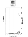
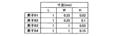
分極処理におけるクラックの発生率は、粘着シート10に対して垂直に見た場合における、半製品20の面積A1に対する、貫通孔16の面積A2の比率A2/A1に応じて変化する。図4、5は、面積比率A2/A1とクラックの発生率との関係を示している。図4は、貫通孔16が円形である場合の結果を示しており、図5は、貫通孔16が四角形である場合の結果を示している。また、図4、5の実験は、素子B1〜素子B4の4種類のサイズを有する半製品20を用いて行った。図6は、素子B1〜素子B4のサイズを示している。また、図7は、図6の寸法L、W、Hを示している。また、図4、5において、面積比率A2/A1が0%のデータは、貫通孔16が形成されていない場合(すなわち、半製品の下面全体が粘着シートに貼り付けられている場合)の結果を示している。
The rate of occurrence of cracks in the polarization treatment changes according to the ratio A2 / A1 of the area A2 of the through
図4、5から、面積比率A2/A1を0%よりも高くすることで、面積比率A2/A1が0%の場合よりも、クラック発生率が低くなることが分かる。但し、面積比率A2/A1を大きくし過ぎると、粘着シート10で半製品20を安定して保持することが困難となり、クラック発生率が上昇する傾向がある。面積比率A2/A1を、15%以上であり、60%以下にすると、クラック発生率を略ゼロとすることができる。
4 and 5, it can be seen that by increasing the area ratio A2 / A1 higher than 0%, the crack generation rate is lower than when the area ratio A2 / A1 is 0%. However, if the area ratio A2 / A1 is too large, it becomes difficult to stably hold the
なお、分極処理後の圧電素子を粘着シート10から剥離すると、剥離の前後で圧電素子の静電容量(すなわち、電極24と電極26の間の静電容量)が変化する。これは、圧電素子を粘着シート10から剥離すると、圧電体基板22内の応力を開放するように圧電体基板22が変形するためである。図8は、実施例1の製造方法により製造した圧電素子C1(すなわち、貫通孔16を塞ぐように貼り付けられた状態で分極された圧電素子)と、貫通孔が形成されていない粘着テープに貼り付けられた状態で分極された圧電素子C2の静電容量を示している。図8では、粘着シートの剥離前と剥離後のそれぞれの静電容量が示されている。図8に示すように、粘着シートの剥離前においては、実施例1の圧電素子C1の方が、圧電素子C2よりも静電容量が大きい。これは、実施例1の製造方法では、圧電体基板22にクラックが入り難いために、より高い電界で分極処理を行うことができるためである。粘着シートを剥離すると、何れの圧電素子でも静電容量が上昇する。このとき、圧電素子C2では、実施例1の圧電素子C1よりも静電容量の変化率が大きくなる(但し、剥離後の静電容量は、実施例1の圧電素子C1の方が大きい)。これは、圧電素子C2に対する分極処理では粘着テープによって圧電体基板の変形が抑制されるため、粘着テープの剥離前に圧電素子C2の圧電体基板中に高い応力が残存しており、粘着テープを剥離するときにその応力が開放されて圧電体基板のドメインの整列状態が変化するためだと考えられる。圧電素子C2では粘着テープの剥離の前後における静電容量の変化率が25%よりも大きいのに対し、実施例1の圧電素子では粘着テープの剥離の前後における静電容量の変化率が25%以下である。実施例1の圧電素子のように、粘着テープの剥離の前後における静電容量変化率が25%以下となるように分極処理を行うことで、より静電容量が高い圧電素子を製造することができる。つまり十分に分極処理された圧電素子を製造することができる。また、このように粘着テープの剥離時の静電容量の変化率が小さいと、圧電素子の製造工程における特性の管理が容易となる。
In addition, when the piezoelectric element after polarization treatment is peeled from the
次に、実施例2の圧電素子の製造方法について説明する。実施例2でも、図1、2に示すように粘着シート10に貼り付けられた半製品20に対して分極処理を行う。実施例2では、図9に示すように、上面側の各電極24に対してプローブピン34を接触させ、下面側の各電極26に対してプローブピン32を接触させる。ここでは、プローブピン32、34によって半製品20の重心20aを挟み込むように、プローブピン32、34をセットする。次に、プローブピン32、34の間に交流電圧を印加する。すなわち、各半製品20の電極24と電極26の間に、交流電圧を印加する。これによって、各半製品20の圧電体基板22に対して交流の電界が印加される。すなわち、実施例2の製造方法では、交流電界によって圧電体基板22を分極させる。交流電界による分極を行う場合にも、貫通孔16上に圧電体基板22を配置することで、粘着シート10によって圧電体基板22が拘束されることを抑制することができる。これによって、圧電体基板22中に高い応力が生じることを抑制し、圧電体基板22にクラックが生じることを抑制することができる。したがって、この製造方法によれば、より大きい交流電界によって圧電体基板22を分極させることが可能である。これによって、電極24と電極26の間の静電容量を大きく変化させることができる。したがって、高い圧電効果が得られる圧電素子を製造することができる。
Next, a method for manufacturing the piezoelectric element of Example 2 will be described. Also in Example 2, as shown in FIGS. 1 and 2, the polarization treatment is performed on the
なお、図9に示すように、交流電界を圧電体基板22に印加すると、圧電体基板22(すなわち、半製品20)は重心20aを中心にして対象に歪が発生する。プローブピン32、34によって各半製品20の重心20aを挟み込むと、プローブピンが接触した部分は歪まないため、プローブピン32、34を半製品20に好適に接触させることができ、適切に分極処理を実施することができる。
As shown in FIG. 9, when an AC electric field is applied to the
なお、上述した実施例1、2では、図2に示すように貫通孔16の全体が半製品20によって塞がれている場合について説明したが、図10に示すように貫通孔16が部分的に半製品20によって塞がれていてもよい。このような構成でも、分極処理時に圧電体基板22の変形が許容されて、圧電体基板22にクラックが生じ難くなる。なお、このような構成においては、半製品20によって塞がれている部分の貫通孔16の面積A2は、図10においてハッチングされている部分の面積となる。この面積A2から得られる面積比率A2/A1が15%以上であり、かつ、60%以下であれば、クラックの発生率をより低減することができる。
In the first and second embodiments described above, the case where the entire through
また、圧電体基板22の厚みが150μm以下である場合には、分極処理時に圧電体基板22にクラックが特に生じ易い。したがって、本明細書に開示の技術は、厚みが150μm以下の圧電体基板22を有する半製品20に対して特に有用である。
Further, when the thickness of the
以上、本発明の具体例を詳細に説明したが、これらは例示にすぎず、特許請求の範囲を限定するものではない。特許請求の範囲に記載の技術には、以上に例示した具体例をさまざまに変形、変更したものが含まれる。
本明細書または図面に説明した技術要素は、単独であるいは各種の組み合わせによって技術的有用性を発揮するものであり、出願時請求項記載の組み合わせに限定されるものではない。また、本明細書または図面に例示した技術は複数目的を同時に達成するものであり、そのうちの一つの目的を達成すること自体で技術的有用性を持つものである。
Specific examples of the present invention have been described in detail above, but these are merely examples and do not limit the scope of the claims. The technology described in the claims includes various modifications and changes of the specific examples illustrated above.
The technical elements described in this specification or the drawings exhibit technical usefulness alone or in various combinations, and are not limited to the combinations described in the claims at the time of filing. In addition, the technology illustrated in the present specification or the drawings achieves a plurality of objects at the same time, and has technical utility by achieving one of the objects.
10:粘着シート
12:接着剤層
14:樹脂フィルム
16:貫通孔
20:半製品
22:圧電体基板
24、26:電極
30:共通電極板
32:プローブピン
34:プローブピン
10: Adhesive sheet 12: Adhesive layer 14: Resin film 16: Through hole 20: Semi-finished product 22:
Claims (6)
粘着シートに貼り付けられた半製品に電圧を印加するステップを有しており、
粘着シートには、貫通孔が形成されており、
半製品は、圧電体基板と、圧電体基板の一方の表面に形成された第1電極と、圧電体基板の他方の表面に形成された第2電極を有しており、
前記ステップでは、第2電極が粘着シートに貼り付けられており、半製品によって貫通孔の少なくとも一部が塞がれている状態で、第1電極と第2電極の間に電圧を印加する、
ことを特徴とする製造方法。 A method for manufacturing a piezoelectric element, comprising:
Having a step of applying a voltage to the semi-finished product attached to the adhesive sheet;
Through-holes are formed in the adhesive sheet,
The semi-finished product has a piezoelectric substrate, a first electrode formed on one surface of the piezoelectric substrate, and a second electrode formed on the other surface of the piezoelectric substrate,
In the step, a voltage is applied between the first electrode and the second electrode in a state where the second electrode is attached to the adhesive sheet and at least a part of the through hole is blocked by the semi-finished product.
The manufacturing method characterized by the above-mentioned.
Priority Applications (1)
| Application Number | Priority Date | Filing Date | Title |
|---|---|---|---|
| JP2012023261A JP5926063B2 (en) | 2012-02-06 | 2012-02-06 | Method for manufacturing piezoelectric element |
Applications Claiming Priority (1)
| Application Number | Priority Date | Filing Date | Title |
|---|---|---|---|
| JP2012023261A JP5926063B2 (en) | 2012-02-06 | 2012-02-06 | Method for manufacturing piezoelectric element |
Publications (2)
| Publication Number | Publication Date |
|---|---|
| JP2013161970A true JP2013161970A (en) | 2013-08-19 |
| JP5926063B2 JP5926063B2 (en) | 2016-05-25 |
Family
ID=49173978
Family Applications (1)
| Application Number | Title | Priority Date | Filing Date |
|---|---|---|---|
| JP2012023261A Expired - Fee Related JP5926063B2 (en) | 2012-02-06 | 2012-02-06 | Method for manufacturing piezoelectric element |
Country Status (1)
| Country | Link |
|---|---|
| JP (1) | JP5926063B2 (en) |
Cited By (3)
| Publication number | Priority date | Publication date | Assignee | Title |
|---|---|---|---|---|
| WO2019054336A1 (en) * | 2017-09-12 | 2019-03-21 | 日本碍子株式会社 | Method for producing piezoelectric element |
| WO2019054337A1 (en) * | 2017-09-12 | 2019-03-21 | 日本碍子株式会社 | Method for inspecting piezoelectric element |
| JP2020165887A (en) * | 2019-03-29 | 2020-10-08 | 凸版印刷株式会社 | Piezoelectric laminated sheet, manufacturing method therefor, piezoelectric sensor, and manufacturing method therefor |
Citations (7)
| Publication number | Priority date | Publication date | Assignee | Title |
|---|---|---|---|---|
| JPS61127658U (en) * | 1985-01-29 | 1986-08-11 | ||
| JP2001168410A (en) * | 1999-09-27 | 2001-06-22 | Matsushita Electric Works Ltd | Polarization processing method and device thereof |
| JP2002176209A (en) * | 2000-12-05 | 2002-06-21 | Murata Mfg Co Ltd | Polarizing apparatus and method |
| JP2002190457A (en) * | 2000-12-20 | 2002-07-05 | Fdk Corp | Method for manufacturing and handling element having directivity |
| JP2004260176A (en) * | 2003-02-25 | 2004-09-16 | Palo Alto Research Center Inc | Tape and its manufacturing method |
| WO2008023686A1 (en) * | 2006-08-23 | 2008-02-28 | Ngk Insulators, Ltd. | Piezoelectric actuator element for ultrasonic motor |
| JP2011018682A (en) * | 2009-07-07 | 2011-01-27 | Konica Minolta Medical & Graphic Inc | Organic piezoelectric material, ultrasonic vibrator and method of manufacturing the same, ultrasonic probe and ultrasonic medical-use image diagnostic equipment |
-
2012
- 2012-02-06 JP JP2012023261A patent/JP5926063B2/en not_active Expired - Fee Related
Patent Citations (7)
| Publication number | Priority date | Publication date | Assignee | Title |
|---|---|---|---|---|
| JPS61127658U (en) * | 1985-01-29 | 1986-08-11 | ||
| JP2001168410A (en) * | 1999-09-27 | 2001-06-22 | Matsushita Electric Works Ltd | Polarization processing method and device thereof |
| JP2002176209A (en) * | 2000-12-05 | 2002-06-21 | Murata Mfg Co Ltd | Polarizing apparatus and method |
| JP2002190457A (en) * | 2000-12-20 | 2002-07-05 | Fdk Corp | Method for manufacturing and handling element having directivity |
| JP2004260176A (en) * | 2003-02-25 | 2004-09-16 | Palo Alto Research Center Inc | Tape and its manufacturing method |
| WO2008023686A1 (en) * | 2006-08-23 | 2008-02-28 | Ngk Insulators, Ltd. | Piezoelectric actuator element for ultrasonic motor |
| JP2011018682A (en) * | 2009-07-07 | 2011-01-27 | Konica Minolta Medical & Graphic Inc | Organic piezoelectric material, ultrasonic vibrator and method of manufacturing the same, ultrasonic probe and ultrasonic medical-use image diagnostic equipment |
Cited By (9)
| Publication number | Priority date | Publication date | Assignee | Title |
|---|---|---|---|---|
| WO2019054336A1 (en) * | 2017-09-12 | 2019-03-21 | 日本碍子株式会社 | Method for producing piezoelectric element |
| WO2019054337A1 (en) * | 2017-09-12 | 2019-03-21 | 日本碍子株式会社 | Method for inspecting piezoelectric element |
| JPWO2019054337A1 (en) * | 2017-09-12 | 2020-08-27 | 日本碍子株式会社 | Piezoelectric element inspection method |
| JPWO2019054336A1 (en) * | 2017-09-12 | 2020-08-27 | 日本碍子株式会社 | Piezoelectric element manufacturing method |
| US11262394B2 (en) | 2017-09-12 | 2022-03-01 | Ngk Insulators, Ltd. | Method for inspecting piezoelectric element |
| US11515470B2 (en) | 2017-09-12 | 2022-11-29 | Ngk Insulators, Ltd. | Method for producing piezoelectric element |
| JP7201603B2 (en) | 2017-09-12 | 2023-01-10 | 日本碍子株式会社 | Piezoelectric element manufacturing method |
| JP2020165887A (en) * | 2019-03-29 | 2020-10-08 | 凸版印刷株式会社 | Piezoelectric laminated sheet, manufacturing method therefor, piezoelectric sensor, and manufacturing method therefor |
| JP7238546B2 (en) | 2019-03-29 | 2023-03-14 | 凸版印刷株式会社 | Piezoelectric laminated sheet, method for producing piezoelectric laminated sheet, piezoelectric sensor, and method for producing piezoelectric sensor |
Also Published As
| Publication number | Publication date |
|---|---|
| JP5926063B2 (en) | 2016-05-25 |
Similar Documents
| Publication | Publication Date | Title |
|---|---|---|
| WO2019237632A1 (en) | Flexible screen and preparation method therefor, and flexible electronic apparatus | |
| US8549715B2 (en) | Piezoelectric microspeaker and method of fabricating the same | |
| TW200810010A (en) | Electrostatic chuck | |
| JP5926063B2 (en) | Method for manufacturing piezoelectric element | |
| TW201735338A (en) | Magnetic sensor and method of manufacturing the same | |
| KR20150124929A (en) | Method for fabricating a magnetoresistive device | |
| JP2008205888A5 (en) | ||
| TW202139783A (en) | Method for polarizing piezoelectric film | |
| JP5100915B2 (en) | Manufacturing method of sensor element provided with PZT film | |
| TWI542722B (en) | Clamp device for use in sputtering process of wafer fabrication, and method of sputtering and electroplating semiconductor package | |
| CN206457248U (en) | A kind of MEMS chip | |
| JP2020170868A5 (en) | ||
| WO2012026421A1 (en) | Electrostatic chuck apparatus and method for manufacturing same | |
| JP2016146429A (en) | Semiconductor device manufacturing method | |
| JPWO2010150351A1 (en) | Electrode substrate | |
| US20140002058A1 (en) | Triaxial piezoelectric sensor | |
| JP2013211475A (en) | Substrate and semiconductor device | |
| KR20180035988A (en) | Substrate structure for lift off | |
| JP5795272B2 (en) | Method for manufacturing ceramic element | |
| TWI673176B (en) | Input device and manufacturing method thereof | |
| CN111769040A (en) | Method for implanting ions into piezoelectric wafer, implantation piece, piezoelectric film and electronic component | |
| KR101715767B1 (en) | Piezoelectric element for Piezoelectric Speaker | |
| CN108933041A (en) | Thin film capacitor and method for manufacturing the same | |
| CN204068888U (en) | Piezoelectric vibrator | |
| KR20130038972A (en) | Method for manufacturing a flexible solid-state secondary battery using neutral mechanical plane and the flexible solid-state secondary battery manufactured by the same |
Legal Events
| Date | Code | Title | Description |
|---|---|---|---|
| A621 | Written request for application examination |
Free format text: JAPANESE INTERMEDIATE CODE: A621 Effective date: 20141118 |
|
| A977 | Report on retrieval |
Free format text: JAPANESE INTERMEDIATE CODE: A971007 Effective date: 20151009 |
|
| A131 | Notification of reasons for refusal |
Free format text: JAPANESE INTERMEDIATE CODE: A131 Effective date: 20151020 |
|
| A521 | Request for written amendment filed |
Free format text: JAPANESE INTERMEDIATE CODE: A523 Effective date: 20151211 |
|
| TRDD | Decision of grant or rejection written | ||
| A01 | Written decision to grant a patent or to grant a registration (utility model) |
Free format text: JAPANESE INTERMEDIATE CODE: A01 Effective date: 20160405 |
|
| A61 | First payment of annual fees (during grant procedure) |
Free format text: JAPANESE INTERMEDIATE CODE: A61 Effective date: 20160421 |
|
| R150 | Certificate of patent or registration of utility model |
Ref document number: 5926063 Country of ref document: JP Free format text: JAPANESE INTERMEDIATE CODE: R150 |
|
| LAPS | Cancellation because of no payment of annual fees |