JP2004260176A - Tape and its manufacturing method - Google Patents
Tape and its manufacturing method Download PDFInfo
- Publication number
- JP2004260176A JP2004260176A JP2004045563A JP2004045563A JP2004260176A JP 2004260176 A JP2004260176 A JP 2004260176A JP 2004045563 A JP2004045563 A JP 2004045563A JP 2004045563 A JP2004045563 A JP 2004045563A JP 2004260176 A JP2004260176 A JP 2004260176A
- Authority
- JP
- Japan
- Prior art keywords
- tape
- conductive layer
- substrate
- conductive
- piezoelectric element
- Prior art date
- Legal status (The legal status is an assumption and is not a legal conclusion. Google has not performed a legal analysis and makes no representation as to the accuracy of the status listed.)
- Granted
Links
- 238000004519 manufacturing process Methods 0.000 title claims description 15
- 239000000463 material Substances 0.000 claims abstract description 38
- 239000000919 ceramic Substances 0.000 claims abstract description 12
- 239000000758 substrate Substances 0.000 claims description 122
- 238000000151 deposition Methods 0.000 claims description 14
- 229920000642 polymer Polymers 0.000 claims description 14
- 238000001465 metallisation Methods 0.000 claims description 12
- 229910010293 ceramic material Inorganic materials 0.000 claims description 9
- 230000005290 antiferromagnetic effect Effects 0.000 claims description 6
- 238000009826 distribution Methods 0.000 claims description 3
- 238000005137 deposition process Methods 0.000 claims description 2
- 239000010410 layer Substances 0.000 description 71
- 229910052751 metal Inorganic materials 0.000 description 46
- 239000002184 metal Substances 0.000 description 46
- 238000000034 method Methods 0.000 description 43
- 230000008018 melting Effects 0.000 description 33
- 238000002844 melting Methods 0.000 description 33
- 239000004593 Epoxy Substances 0.000 description 25
- KDLHZDBZIXYQEI-UHFFFAOYSA-N Palladium Chemical compound [Pd] KDLHZDBZIXYQEI-UHFFFAOYSA-N 0.000 description 15
- 239000010409 thin film Substances 0.000 description 15
- 238000010586 diagram Methods 0.000 description 14
- 238000005304 joining Methods 0.000 description 12
- 239000000945 filler Substances 0.000 description 11
- 239000011521 glass Substances 0.000 description 9
- 239000011888 foil Substances 0.000 description 8
- 238000005498 polishing Methods 0.000 description 8
- 230000008021 deposition Effects 0.000 description 7
- 238000013461 design Methods 0.000 description 7
- 239000010408 film Substances 0.000 description 7
- 239000007791 liquid phase Substances 0.000 description 7
- 230000001052 transient effect Effects 0.000 description 7
- 239000004020 conductor Substances 0.000 description 6
- HFGPZNIAWCZYJU-UHFFFAOYSA-N lead zirconate titanate Chemical compound [O-2].[O-2].[O-2].[O-2].[O-2].[Ti+4].[Zr+4].[Pb+2] HFGPZNIAWCZYJU-UHFFFAOYSA-N 0.000 description 6
- 229910052451 lead zirconate titanate Inorganic materials 0.000 description 6
- 230000005855 radiation Effects 0.000 description 6
- 229910045601 alloy Inorganic materials 0.000 description 5
- 239000000956 alloy Substances 0.000 description 5
- 239000010931 gold Substances 0.000 description 5
- 239000010949 copper Substances 0.000 description 4
- 229910000765 intermetallic Inorganic materials 0.000 description 4
- 229910052763 palladium Inorganic materials 0.000 description 4
- 239000011248 coating agent Substances 0.000 description 3
- 238000000576 coating method Methods 0.000 description 3
- 229910052802 copper Inorganic materials 0.000 description 3
- 229910052737 gold Inorganic materials 0.000 description 3
- 229910052738 indium Inorganic materials 0.000 description 3
- 238000002834 transmittance Methods 0.000 description 3
- CSCPPACGZOOCGX-UHFFFAOYSA-N Acetone Chemical compound CC(C)=O CSCPPACGZOOCGX-UHFFFAOYSA-N 0.000 description 2
- 239000002885 antiferromagnetic material Substances 0.000 description 2
- 238000003491 array Methods 0.000 description 2
- 150000001875 compounds Chemical class 0.000 description 2
- 238000001514 detection method Methods 0.000 description 2
- NKZSPGSOXYXWQA-UHFFFAOYSA-N dioxido(oxo)titanium;lead(2+) Chemical compound [Pb+2].[O-][Ti]([O-])=O NKZSPGSOXYXWQA-UHFFFAOYSA-N 0.000 description 2
- APFVFJFRJDLVQX-UHFFFAOYSA-N indium atom Chemical compound [In] APFVFJFRJDLVQX-UHFFFAOYSA-N 0.000 description 2
- 238000003780 insertion Methods 0.000 description 2
- 230000037431 insertion Effects 0.000 description 2
- 238000007689 inspection Methods 0.000 description 2
- 239000011810 insulating material Substances 0.000 description 2
- 150000002739 metals Chemical class 0.000 description 2
- 239000000203 mixture Substances 0.000 description 2
- 238000012986 modification Methods 0.000 description 2
- 230000004048 modification Effects 0.000 description 2
- 238000007650 screen-printing Methods 0.000 description 2
- 229910052709 silver Inorganic materials 0.000 description 2
- 239000002344 surface layer Substances 0.000 description 2
- 230000003746 surface roughness Effects 0.000 description 2
- 229910052718 tin Inorganic materials 0.000 description 2
- 238000012546 transfer Methods 0.000 description 2
- 229920002799 BoPET Polymers 0.000 description 1
- RYGMFSIKBFXOCR-UHFFFAOYSA-N Copper Chemical compound [Cu] RYGMFSIKBFXOCR-UHFFFAOYSA-N 0.000 description 1
- WHXSMMKQMYFTQS-UHFFFAOYSA-N Lithium Chemical compound [Li] WHXSMMKQMYFTQS-UHFFFAOYSA-N 0.000 description 1
- 239000005041 Mylar™ Substances 0.000 description 1
- BQCADISMDOOEFD-UHFFFAOYSA-N Silver Chemical compound [Ag] BQCADISMDOOEFD-UHFFFAOYSA-N 0.000 description 1
- 239000004809 Teflon Substances 0.000 description 1
- 229920006362 Teflon® Polymers 0.000 description 1
- ATJFFYVFTNAWJD-UHFFFAOYSA-N Tin Chemical compound [Sn] ATJFFYVFTNAWJD-UHFFFAOYSA-N 0.000 description 1
- FKSZLDCMQZJMFN-UHFFFAOYSA-N [Mg].[Pb] Chemical compound [Mg].[Pb] FKSZLDCMQZJMFN-UHFFFAOYSA-N 0.000 description 1
- 238000010521 absorption reaction Methods 0.000 description 1
- NIXOWILDQLNWCW-UHFFFAOYSA-N acrylic acid group Chemical group C(C=C)(=O)O NIXOWILDQLNWCW-UHFFFAOYSA-N 0.000 description 1
- 239000000443 aerosol Substances 0.000 description 1
- 230000004075 alteration Effects 0.000 description 1
- PNEYBMLMFCGWSK-UHFFFAOYSA-N aluminium oxide Inorganic materials [O-2].[O-2].[O-2].[Al+3].[Al+3] PNEYBMLMFCGWSK-UHFFFAOYSA-N 0.000 description 1
- 230000005540 biological transmission Effects 0.000 description 1
- 230000015572 biosynthetic process Effects 0.000 description 1
- 239000000969 carrier Substances 0.000 description 1
- 238000004140 cleaning Methods 0.000 description 1
- 239000002131 composite material Substances 0.000 description 1
- PMHQVHHXPFUNSP-UHFFFAOYSA-M copper(1+);methylsulfanylmethane;bromide Chemical compound Br[Cu].CSC PMHQVHHXPFUNSP-UHFFFAOYSA-M 0.000 description 1
- 239000013078 crystal Substances 0.000 description 1
- 238000005520 cutting process Methods 0.000 description 1
- 230000000694 effects Effects 0.000 description 1
- 239000000835 fiber Substances 0.000 description 1
- PCHJSUWPFVWCPO-UHFFFAOYSA-N gold Chemical compound [Au] PCHJSUWPFVWCPO-UHFFFAOYSA-N 0.000 description 1
- 238000010438 heat treatment Methods 0.000 description 1
- 238000009413 insulation Methods 0.000 description 1
- 150000002500 ions Chemical class 0.000 description 1
- 229910052744 lithium Inorganic materials 0.000 description 1
- FUJCRWPEOMXPAD-UHFFFAOYSA-N lithium oxide Chemical compound [Li+].[Li+].[O-2] FUJCRWPEOMXPAD-UHFFFAOYSA-N 0.000 description 1
- 229910001947 lithium oxide Inorganic materials 0.000 description 1
- CPLXHLVBOLITMK-UHFFFAOYSA-N magnesium oxide Inorganic materials [Mg]=O CPLXHLVBOLITMK-UHFFFAOYSA-N 0.000 description 1
- 239000000395 magnesium oxide Substances 0.000 description 1
- AXZKOIWUVFPNLO-UHFFFAOYSA-N magnesium;oxygen(2-) Chemical compound [O-2].[Mg+2] AXZKOIWUVFPNLO-UHFFFAOYSA-N 0.000 description 1
- 238000013017 mechanical damping Methods 0.000 description 1
- 230000007935 neutral effect Effects 0.000 description 1
- 229910052758 niobium Inorganic materials 0.000 description 1
- 239000010955 niobium Substances 0.000 description 1
- GUCVJGMIXFAOAE-UHFFFAOYSA-N niobium atom Chemical compound [Nb] GUCVJGMIXFAOAE-UHFFFAOYSA-N 0.000 description 1
- 239000002245 particle Substances 0.000 description 1
- 239000012071 phase Substances 0.000 description 1
- 238000007639 printing Methods 0.000 description 1
- 229910052594 sapphire Inorganic materials 0.000 description 1
- 239000010980 sapphire Substances 0.000 description 1
- 230000035945 sensitivity Effects 0.000 description 1
- 239000004332 silver Substances 0.000 description 1
- 239000010944 silver (metal) Substances 0.000 description 1
- 238000005245 sintering Methods 0.000 description 1
- 239000006104 solid solution Substances 0.000 description 1
- VEALVRVVWBQVSL-UHFFFAOYSA-N strontium titanate Chemical compound [Sr+2].[O-][Ti]([O-])=O VEALVRVVWBQVSL-UHFFFAOYSA-N 0.000 description 1
- 238000012360 testing method Methods 0.000 description 1
Images


Classifications
-
- G—PHYSICS
- G01—MEASURING; TESTING
- G01N—INVESTIGATING OR ANALYSING MATERIALS BY DETERMINING THEIR CHEMICAL OR PHYSICAL PROPERTIES
- G01N29/00—Investigating or analysing materials by the use of ultrasonic, sonic or infrasonic waves; Visualisation of the interior of objects by transmitting ultrasonic or sonic waves through the object
- G01N29/22—Details, e.g. general constructional or apparatus details
- G01N29/24—Probes
- G01N29/2437—Piezoelectric probes
- G01N29/245—Ceramic probes, e.g. lead zirconate titanate [PZT] probes
-
- B—PERFORMING OPERATIONS; TRANSPORTING
- B06—GENERATING OR TRANSMITTING MECHANICAL VIBRATIONS IN GENERAL
- B06B—METHODS OR APPARATUS FOR GENERATING OR TRANSMITTING MECHANICAL VIBRATIONS OF INFRASONIC, SONIC, OR ULTRASONIC FREQUENCY, e.g. FOR PERFORMING MECHANICAL WORK IN GENERAL
- B06B1/00—Methods or apparatus for generating mechanical vibrations of infrasonic, sonic, or ultrasonic frequency
- B06B1/02—Methods or apparatus for generating mechanical vibrations of infrasonic, sonic, or ultrasonic frequency making use of electrical energy
- B06B1/06—Methods or apparatus for generating mechanical vibrations of infrasonic, sonic, or ultrasonic frequency making use of electrical energy operating with piezoelectric effect or with electrostriction
- B06B1/0607—Methods or apparatus for generating mechanical vibrations of infrasonic, sonic, or ultrasonic frequency making use of electrical energy operating with piezoelectric effect or with electrostriction using multiple elements
- B06B1/0622—Methods or apparatus for generating mechanical vibrations of infrasonic, sonic, or ultrasonic frequency making use of electrical energy operating with piezoelectric effect or with electrostriction using multiple elements on one surface
-
- G—PHYSICS
- G01—MEASURING; TESTING
- G01L—MEASURING FORCE, STRESS, TORQUE, WORK, MECHANICAL POWER, MECHANICAL EFFICIENCY, OR FLUID PRESSURE
- G01L1/00—Measuring force or stress, in general
- G01L1/16—Measuring force or stress, in general using properties of piezoelectric devices
-
- G—PHYSICS
- G01—MEASURING; TESTING
- G01N—INVESTIGATING OR ANALYSING MATERIALS BY DETERMINING THEIR CHEMICAL OR PHYSICAL PROPERTIES
- G01N29/00—Investigating or analysing materials by the use of ultrasonic, sonic or infrasonic waves; Visualisation of the interior of objects by transmitting ultrasonic or sonic waves through the object
- G01N29/22—Details, e.g. general constructional or apparatus details
- G01N29/24—Probes
- G01N29/2475—Embedded probes, i.e. probes incorporated in objects to be inspected
-
- H—ELECTRICITY
- H10—SEMICONDUCTOR DEVICES; ELECTRIC SOLID-STATE DEVICES NOT OTHERWISE PROVIDED FOR
- H10N—ELECTRIC SOLID-STATE DEVICES NOT OTHERWISE PROVIDED FOR
- H10N30/00—Piezoelectric or electrostrictive devices
- H10N30/01—Manufacture or treatment
- H10N30/07—Forming of piezoelectric or electrostrictive parts or bodies on an electrical element or another base
- H10N30/072—Forming of piezoelectric or electrostrictive parts or bodies on an electrical element or another base by laminating or bonding of piezoelectric or electrostrictive bodies
- H10N30/073—Forming of piezoelectric or electrostrictive parts or bodies on an electrical element or another base by laminating or bonding of piezoelectric or electrostrictive bodies by fusion of metals or by adhesives
-
- H—ELECTRICITY
- H10—SEMICONDUCTOR DEVICES; ELECTRIC SOLID-STATE DEVICES NOT OTHERWISE PROVIDED FOR
- H10N—ELECTRIC SOLID-STATE DEVICES NOT OTHERWISE PROVIDED FOR
- H10N30/00—Piezoelectric or electrostrictive devices
- H10N30/01—Manufacture or treatment
- H10N30/07—Forming of piezoelectric or electrostrictive parts or bodies on an electrical element or another base
- H10N30/074—Forming of piezoelectric or electrostrictive parts or bodies on an electrical element or another base by depositing piezoelectric or electrostrictive layers, e.g. aerosol or screen printing
-
- H—ELECTRICITY
- H10—SEMICONDUCTOR DEVICES; ELECTRIC SOLID-STATE DEVICES NOT OTHERWISE PROVIDED FOR
- H10N—ELECTRIC SOLID-STATE DEVICES NOT OTHERWISE PROVIDED FOR
- H10N39/00—Integrated devices, or assemblies of multiple devices, comprising at least one piezoelectric, electrostrictive or magnetostrictive element covered by groups H10N30/00 – H10N35/00
-
- G—PHYSICS
- G01—MEASURING; TESTING
- G01N—INVESTIGATING OR ANALYSING MATERIALS BY DETERMINING THEIR CHEMICAL OR PHYSICAL PROPERTIES
- G01N2291/00—Indexing codes associated with group G01N29/00
- G01N2291/02—Indexing codes associated with the analysed material
- G01N2291/028—Material parameters
- G01N2291/02827—Elastic parameters, strength or force
-
- G—PHYSICS
- G01—MEASURING; TESTING
- G01N—INVESTIGATING OR ANALYSING MATERIALS BY DETERMINING THEIR CHEMICAL OR PHYSICAL PROPERTIES
- G01N2291/00—Indexing codes associated with group G01N29/00
- G01N2291/26—Scanned objects
- G01N2291/269—Various geometry objects
- G01N2291/2694—Wings or other aircraft parts
Abstract
Description
本発明は、テープおよびその製造方法に関する。 The present invention relates to a tape and a method for manufacturing the tape.
圧電セラミックスを用いたテープ及び製造方法が知られている。 A tape using piezoelectric ceramics and a manufacturing method are known.
圧電セラミックスの重大な欠点は、材料の脆性のため薄く大きな(数センチメートル〜数十センチメートル規模の)シート状に構成するのが困難なことである。 A significant disadvantage of piezoelectric ceramics is that it is difficult to configure them into thin, large (several centimeters to tens of centimeter scale) sheets due to the brittleness of the material.
本発明のテープは、第1の可撓導電層と、第1の導電層に対向して配置した第2の可撓導電層とを含む。センサ、アクチュエータ、またはトランスデューサのうちの少なくとも1つからなる複数の素子を、第1の可撓導電層と第2の可撓導電層との間に配置し、かつ両導電層上に接合する。センサ、アクチュエータ、またはトランスデューサのうちの少なくとも1つからなる複数の素子の周囲には絶縁材を挿入する。第1および第2の可撓導電層に電気接点網を接続して、可撓検出検査テープに電力および制御信号を付与する。 The tape of the present invention includes a first flexible conductive layer, and a second flexible conductive layer disposed to face the first conductive layer. A plurality of elements comprising at least one of a sensor, an actuator, or a transducer are disposed between the first flexible conductive layer and the second flexible conductive layer, and are bonded on both conductive layers. An insulating material is inserted around a plurality of elements including at least one of a sensor, an actuator, and a transducer. An electrical contact network is connected to the first and second flexible conductive layers to apply power and control signals to the flexible detection test tape.
テープであって、少なくとも部分的に可撓性のある第1の導電層と、少なくとも部分的に可撓性があり、前記第1の導電層に対向して配置される第2の導電層と、前記第1の導電層と前記第2の導電層との間に配置され接合されるセンサ、アクチュエータ、またはトランスデューサのうちの少なくとも1つからなる複数の素子と、前記第1の導電層と前記第2の導電層とに接続し、前記可テープに電力および制御信号を印加する電気接点網とを含むことを特徴とする。 A tape, a first conductive layer that is at least partially flexible, and a second conductive layer that is at least partially flexible and that is disposed opposite the first conductive layer. A plurality of elements consisting of at least one of a sensor, an actuator, and a transducer arranged and joined between the first conductive layer and the second conductive layer; and An electrical contact network connected to the second conductive layer for applying power and control signals to the tape.
上記テープにおいて、前記複数のセンサ、アクチュエータ、またはトランスデューサは、分類されグループとして制御されると好適である。 In the tape, the plurality of sensors, actuators, or transducers are preferably classified and controlled as a group.
上記テープにおいて、前記センサ、アクチュエータ、またはトランスデューサのうちの少なくとも1つは、多様な異なる幾何学的形状に形成されると好適である。 In the tape, at least one of the sensor, the actuator, or the transducer is preferably formed in various different geometric shapes.
上記テープにおいて、前記センサ、アクチュエータ、またはトランスデューサのうちの少なくとも1つは、前記センサ、アクチュエータ、またはトランスデューサの密度が不均一となるように前記テープ上に配置された複数のセンサ、アクチュエータ、またはトランスデューサであると好適である。 In the tape, at least one of the sensors, actuators, or transducers is a plurality of sensors, actuators, or transducers disposed on the tape such that the sensor, actuator, or transducer has a non-uniform density. It is preferred that
上記テープにおいて、前記第1の導電層および前記第2の導電層の少なくともいずれかは、前記センサ、アクチュエータ、またはトランスデューサのうちの少なくとも1つの形状および分布に対応してパターニングしたメタライゼーション層を有するポリマーテープであると好適である。 In the above-mentioned tape, at least one of the first conductive layer and the second conductive layer has a metallization layer patterned according to a shape and distribution of at least one of the sensor, the actuator, and the transducer. Suitably, it is a polymer tape.
上記テープにおいて、前記センサ、アクチュエータ、またはトランスデューサの少なくとも1つのうち、ある素子は圧電素子を含む1つの機能セラミック材料から構成され、他の素子は1つ以上の他の機能セラミック材料から構成されると好適である。 In the above-mentioned tape, among the at least one of the sensor, the actuator, and the transducer, one element is made of one functional ceramic material including a piezoelectric element, and another element is made of one or more other functional ceramic materials. It is suitable.
上記テープにおいて、前記複数のアクチュエータ、センサ、またはトランスデューサは、堆積工程によって形成した反強磁性、電歪、または磁歪素子構造を含む複数の他の機能セラミック材料であり、前記反強磁性またはその他の機能セラミック素子構造の第1の表面上に第1の電極が堆積され、前記反強磁性またはその他の機能セラミック素子構造の第2の表面上に第2の電極が堆積されると好適である。 In the tape, the plurality of actuators, sensors, or transducers are antiferromagnetic, electrostrictive, or other functional ceramic materials including a magnetostrictive element structure formed by a deposition process, and the antiferromagnetic or other Suitably, a first electrode is deposited on a first surface of the functional ceramic element structure and a second electrode is deposited on a second surface of the antiferromagnetic or other functional ceramic element structure.
本発明は、テープの製造方法であって、少なくとも1つの第1の基板表面上に材料を堆積して複数の素子構造を形成するステップと、前記複数の素子構造の各表面上に電極を堆積するステップと、前記素子構造を第2の基板に接合するステップであって、前記第2の基板は導電性をもつかまたは導電層を有し、かつキャリアプレート上に支持されるステップと、前記少なくとも1つの第1の基板を前記素子構造から取外すステップと、第2の側面電極を前記複数の素子構造の第2の表面上に堆積するステップと、前記素子構造の第2の側面を他の基板に接合するステップであって、前記他の基板は導電性をもつかまたは導電層を有するステップと、前記キャリアプレートを取外すステップとを含むことを特徴とする。 The present invention is a method of manufacturing a tape, comprising: depositing a material on at least one first substrate surface to form a plurality of device structures; and depositing an electrode on each surface of the plurality of device structures. Bonding the device structure to a second substrate, the second substrate having conductivity or having a conductive layer, and being supported on a carrier plate; Removing at least one first substrate from the device structure; depositing a second side electrode on a second surface of the plurality of device structures; Bonding to the substrate, the other substrate having a conductive or conductive layer, and removing the carrier plate.
図1は、本願の概念に従う製造方法の第1の実施形態のハイレベル工程フロー図10を示す。以下の説明は圧電厚膜素子(厚さ10μm〜100μm)の製造に関して行うが、開示する方法は他の材料にも利用でき、薄膜素子(厚さ10μm未満)および厚さ100μm超〜ミリメートル単位の素子の製造にも利用できる。 FIG. 1 shows a high-level process flow diagram 10 of a first embodiment of a manufacturing method according to the concepts of the present application. Although the following description will be made with respect to the manufacture of piezoelectric thick film devices (10 μm to 100 μm thick), the disclosed method can be used for other materials, including thin film devices (less than 10 μm thick) and thicknesses greater than 100 μm to millimeters. It can also be used to manufacture devices.
圧電セラミック厚膜素子の作製は、ダイレクトマーキング技術を利用して、ステップ12で圧電材料を適切な基板上に堆積させて行う。作製工程は、密度を高めるため好適には約1100℃〜1350℃で材料を焼結させるステップを含むが、適当な環境下では他の温度範囲を用いてもよい。作製工程に続いて、形成した圧電素子の表面を、ステップ14で好適にはドライテープ研磨技術を用いて研磨する。次にステップ16で、圧電素子の表面上に電極を堆積する。次にステップ18で、圧電素子を最終目標基板に永久接合する。最終目標基板は可撓性があり、かつ導電性があるか、または金属箔もしくは金属化ポリマーテープ等の表面導電層を有する。可撓性のある目標基板を別の剛性のあるキャリアプレート上に設置してもよい。一般的な圧電セラミック素子の組成は、ドーピングした、またはドーピングしていないPZT(ジルコン酸チタン酸鉛)であるが、チタン酸鉛、ジルコン酸鉛、マグネシウムチタン酸鉛、ならびにそのチタン酸鉛、ニオブ酸リチウム、リチウムタンタネート、およびその他との固溶体等の他の任意の圧電材料も使用できる。
The fabrication of the piezoelectric ceramic thick film element is performed by depositing a piezoelectric material on a suitable substrate in
圧電素子を堆積させた基板は、ステップ20でレーザまたは他の適切な装置等からの放射エネルギを利用したリフトオフ工程によって除去する。除去工程は、基板を介して圧電素子を放射線源に露出させ、基板と圧電素子間の付着界面を破壊するステップを含む。完全に基板を除去するため、必要に応じてさらに加熱を行う。リフトオフ工程が完了すると、ステップ22で圧電材料の第2の表面上に第2の電極を堆積する。その後、ステップ24で各素子を高電圧下でポーリングして材料に圧電特性をもたせる。ステップ26で各素子の電気的特性、例えば誘電性を測定して、各素子が要求される規準に合致しているかどうかを確認する。ステップ28で圧電素子間に絶縁フィラーを挿入し、その後、ステップ30で圧電素子を第2の最終目標基板30に接合する。第2の最終目標基板は、金属箔や金属化したポリマーテープ等、可撓性をもつ。その後、組立てた構造をキャリアプレート32から取外すことができる。
The substrate on which the piezoelectric elements have been deposited is removed in
図2は第2のハイレベル工程フロー図40を示す。この工程と図1の工程との違いは、最終目標基板ではなく移動基板に接合を行うことである。従って作製ステップ42、テープ研磨ステップ44、および電極堆積ステップ46は、図1のステップ12,14および16と同様に行う。接合ステップ48では永久接続を意図しないので、移動基板に接合を行う。その後、図1のステップ20,22,24および26に対応するリフトオフステップ50、第2電極堆積ステップ52、ポーリングステップ54、および電気特性検査ステップ56を実施する。
FIG. 2 shows a second high level process flow diagram 40. The difference between this step and the step of FIG. 1 is that the bonding is performed not on the final target substrate but on the moving substrate. Therefore, the
その後、図1のステップ18と同設計の手順で、圧電素子を最終目標基板58に接合する。接合ステップ58に続いて、60で移動基板を除去する。その後、絶縁フィラー挿入ステップ62、第2の最終目標基板への接合ステップ64、およびキャリアプレート除去ステップ66を、図1のステップ28,30および32と同様に実施する。最終目標基板への接合時には、高強度の薄い接合層を使用して、接合層の不要な機械制動または吸収を回避または最小限に抑える。ただしこの接合は、圧電素子上の金属電極と最終目標基板もしくは最終目標基板の導電表面との間の電気接点の維持が可能なものである。
Thereafter, the piezoelectric element is bonded to the
図1および図2の工程は、大型で利用可能な収率の高い、すなわち収率60%超、より好適には90%超、さらに好適には98%超の可撓圧電セラミックテープの製造に適している。 The process of FIGS. 1 and 2 can be used to produce large, high yield flexible piezoelectric ceramic tapes with high yields, ie, greater than 60%, more preferably greater than 90%, and even more preferably greater than 98%. Are suitable.
図3は、上記のステップ12および42を詳細に示す図である。圧電セラミック素子72を適切な基板74上に堆積し、その後1100℃〜1350℃で焼結して高密度にする。堆積ステップは、スクリーン印刷、ジェット印刷、バリスティックエアロゾルマーキング(BAM)、または音響イジェクション等を含む多数のダイレクトマーキング法によって行うことができる。これらの技術の利用により、圧電素子構成の種類および厚さに柔軟性をもたせることができる。
FIG. 3 is a diagram showing the
特に適した基板はサファイアである。その他の利用可能な基板材料には、透明アルミナセラミックス、窒化アルミニウム、酸化マグネシウム、チタン酸ストロンチウム等がある。本工程の一実施形態では、選択される基板は波長308nmで動作するエキシマレーザ用の透明基板で、その結晶方向に制約のない基板である。 A particularly suitable substrate is sapphire. Other available substrate materials include transparent alumina ceramics, aluminum nitride, magnesium oxide, strontium titanate, and the like. In one embodiment of the present process, the substrate selected is a transparent substrate for an excimer laser operating at a wavelength of 308 nm, which is not restricted in the crystal direction.
圧電素子の作製完了後、工程はステップ14(またはステップ44)へ進み、圧電素子の上面をテープ研磨工程によって研磨し、鉛の不足等による何らかの表面損傷層をなくす。 After the completion of the fabrication of the piezoelectric element, the process proceeds to step 14 (or step 44), and the upper surface of the piezoelectric element is polished by a tape polishing step to eliminate any surface damage layer due to lack of lead or the like.
好適な一実施形態では、テープ研磨工程は、圧電素子の表面縁部まで平坦なフラット研磨を行い、各素子上の凸状効果を回避するドライテープ研磨工程である。 In a preferred embodiment, the tape polishing step is a dry tape polishing step of performing flat flat polishing up to the surface edge of the piezoelectric element to avoid a convex effect on each element.
研磨およびクリーニング後、工程はステップ16(またはステップ46)へ進み、図4(A)に示すようにCr/Niまたはその他の適当な材料等の金属電極76を、シャドーマスクを用いたスパッタリングまたは蒸着等の技術によって圧電素子の表面上に堆積する。電極の堆積は、スクリーン印刷等のダイレクトマーキング法の一つによって行い、適当な温度で焼結させることもできる。または薄膜金属間過渡液相接合法を用いる場合は、圧電素子の電極としてある種の低/高溶融点金属の薄膜層を使用してもよく、これにより場合によってはCr/Ni等の電極層をさらに堆積させなくてもよい。ただし、好適には薄膜金属間過渡液相接合法は、Cr/Ni堆積等の金属電極堆積後に行う。この方法については以下で詳述するが、一般には高溶融点金属78(銀(Ag)、金(Au)、銅(Cu)、パラジウム(Pd)等)の薄膜層と、低溶融点金属79(インジウム(In)、錫(Sn)等)の薄膜層とを圧電素子(または基板)上に堆積させ、かつ高溶融点金属(Ag,Au,Cu,Pd等)の薄膜層を基板(または圧電素子)上に堆積させてもよい。これらの材料はその後、接合部の形成に使用される。また、低溶融点金属と高溶融点金属とを交互に重ねた多層構造の薄膜層を使用してもよい。
After polishing and cleaning, the process proceeds to step 16 (or step 46) where a
図5(A)に示すように、最終目標基板82は金属箔等の可撓性のある導電材である(そのため共通電極としても使用可能)。最終目標基板82はまた、本工程中にキャリアプレート80上に設置してもよい。
As shown in FIG. 5A, the
圧電素子72への接合は、薄さ1μm未満まで薄くできる非導電性のエポキシ層84を用いて行う。薄いエポキシはμm単位以下の導電粒子を含み、これは一実施形態では導電球(Au球等)85でもよく、従ってエポキシはZ方向(金属箔表面に対して垂直方向)に導電性をもつ。これにより圧電素子の表面電極と金属箔間に電気的接触を維持できる。導電球の濃度は、硬化後の薄いエポキシがZ方向には導電性をもつが、ただし異方性導電膜のように横方向には導電性をもたないような範囲に制御できる。エポキシが収縮しても表面と球との間にZ方向の接触を維持できる。
The bonding to the
図5(B)および図5(C)では、導電球85を取除き、非導電性エポキシ層84のみを使用して接合を行う。図5(C)により詳細に示すように、圧電素子および/または最終目標基板82の表面粗さまたは凹凸を適当に制御して、電極84の表面と金属箔82とが接触したときに形成される電気接点86を介して電気的接触を維持する。
In FIGS. 5B and 5C, the
他の実施形態では、最終目標基板への接合は、上述した薄膜金属間過渡液相金属接合法を用いて行い、これは一実施形態では、図5(D)に示す高溶融点金属(Ag,Cu,Pd,Au等)−低溶融点金属(In,Sn等)の金属間化合物接合層または合金88を用いる。
In another embodiment, bonding to the final target substrate is performed using the thin film intermetallic transient liquid phase metal bonding method described above, which in one embodiment is a high melting point metal (Ag) shown in FIG. , Cu, Pd, Au, etc.)-Low melting point metal (In, Sn, etc.) intermetallic compound bonding layer or
より特定的には、薄膜金属間過渡液相金属接合には、Pd薄膜層等の高溶融点金属の薄層を目標基板上に堆積する。次に、圧電素子をPd薄層と接触させて、圧力下で低溶融点金属(In)の溶融点超の温度、例えば約200℃で加熱する。この操作により、高溶融点金属/低溶融点金属/高溶融点金属の組み合わせ、例えば、Pd/In/Pd層により高溶融点金属−低溶融点金属の金属間化合物接合層または合金88を形成する(Pd/In層等の高溶融点金属/低溶融点金属は図4(B)に示すように圧電素子上にすでに堆積されている)。この化合物または合金は、厚さ約1μmで圧電素子72と目標基板82とを接合するように作用するPdIn3合金層となりうる。機能的には、低溶融点金属が高溶融点金属中に拡散して化合物/合金を形成する。
More specifically, for thin film intermetallic transient liquid phase metal bonding, a thin layer of a high melting point metal, such as a Pd thin film layer, is deposited on a target substrate. Next, the piezoelectric element is brought into contact with the thin Pd layer and heated under pressure to a temperature above the melting point of the low melting point metal (In), for example, about 200 ° C. With this operation, a high melting point metal / low melting point metal / high melting point metal combination, for example, a high melting point metal-low melting point metal intermetallic compound bonding layer or
形成した金属間化合物相の溶融点は低溶融点金属の溶融点より大幅に高くなりうるので、接合層の動作温度は接合を形成する温度よりもかなり高くなりうる。例えば、低溶融点金属にインジウム(In)を使用し、高溶融点金属にパラジウム(Pd)を使用した場合、Inの溶融点は約156℃なので、接合は200℃以下で完了できる。しかし、形成された金属間化合物接合層PdIn3の溶融点は約664℃であるため、その動作温度は200℃より十分高くなりうる。接合層の厚さは1μm〜10μmが可能であるが、ここでの目的のためにはより薄い接合層(例えば1μm)が求められる。さらに、両金属が金属間接合層の形成に完全に消費されるように高溶融点金属および低溶融点金属の量を制御できる。 Since the melting point of the formed intermetallic compound phase can be significantly higher than the melting point of the low melting point metal, the operating temperature of the bonding layer can be significantly higher than the temperature at which the bond is formed. For example, when indium (In) is used as the low melting point metal and palladium (Pd) is used as the high melting point metal, the melting point of In is about 156 ° C., so that the bonding can be completed at 200 ° C. or less. However, since the melting point of the formed intermetallic compound bonding layer PdIn 3 is about 664 ° C., its operating temperature can be sufficiently higher than 200 ° C. The thickness of the bonding layer can be between 1 μm and 10 μm, but for this purpose a thinner bonding layer (eg 1 μm) is required. Further, the amounts of the high melting point metal and the low melting point metal can be controlled such that both metals are completely consumed in forming the intermetallic bonding layer.
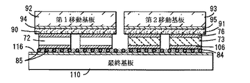
図2の一時的接合工程ステップ48を図6(A)および図6(B)に示す。図6(A)では、接合操作に取外し可能な導電接合エポキシ、例えば3M社製の9712,9713および9719を含む取外し可能な導電テープ90等を使用する。移動基板92は、メタライゼーション層等の表面導電層94を有する金属化したガラスでもよい。図6(B)に示す他の実施形態では、接合操作はμm単位以下の導電球85を含む薄い非導電性エポキシ84を使用して、ITO(導電膜)コーティング100を有するガラス等の移動基板98に接合する。
The temporary
圧電素子を最終目標基板に永久接合する(図1のステップ18)か、または移動基板に一時的に接合する(図2のステップ48)と、次のステップでは圧電素子72を基板74から取外す。基板74の除去は図7(A)および図7(B)に示すようなリフトオフ操作によって行う。以下の説明は図5(A)の構成に基づくが、本明細書に記載する他のあらゆる代替例にも適用できる。まず基板74を、基板74をほぼ透過する波長をもつ放射線源(エキシマレーザ源等)102からの放射ビーム(レーザビーム等)に露出させる。これにより放射ビームの大部分が基板74を通過して、基板と基板表面の素子72との界面に達する。界面でのエネルギが両構成要素間の物理的付着を破壊するように作用する。放射線露出操作に続いて、図7(B)に示すようにヒータ104から熱がかけられる。ヒータからの温度は状況によって異なるが、一実施形態では、残留接点を簡単に除去して圧電素子72を基板74から完全に解放するには40℃〜50℃の温度で十分である。
Once the piezoelectric element is permanently bonded to the final target substrate (
放射線源への露出は圧電素子表面の損傷の可能性を高めるが、この損傷の可能性はわずか厚さ約0.1μm程度にすぎない。どのような表面損傷層も、イオン切削またはテープ研磨を含む適切な方法によって除去可能である。 Exposure to a radiation source increases the likelihood of damage to the piezoelectric element surface, but this damage is only about 0.1 μm thick. Any surface damage layers can be removed by any suitable method, including ion cutting or tape polishing.
次に図8(A)および図8(B)に示すように、シャドーマスクを用いて、または図1のステップ22もしくは図2のステップ52に従う他の適切な方法によって、解放された圧電素子72表面上にCr/Ni等の第2の側面電極106を堆積する。第2電極の堆積後、工程はステップ24および54へそれぞれ進み、圧電素子72を圧電特性を得るのに十分であると当該技術分野で公知の電圧108下でポーリングする。ポーリング後、素子の電気的特性、例えば誘電性を測定する(図1のステップ26、図2のステップ56)。
Next, as shown in FIGS. 8A and 8B, the released
図2の工程による場合のように圧電素子の厚膜アレイを一時的に移動基板に接合する場合は、ステップ58およびステップ60を実行する。
一時的接合を利用すると、圧電アレイを最終目標基板に接合するのは電気的特性の測定後でよい。 With the use of temporary bonding, bonding of the piezoelectric array to the final target substrate may be performed after measuring electrical properties.
図2のステップ58は、図1の接合ステップ18と同様に行うことができる。図9(A)〜図9(D)は、図5(A)および図5(D)の接合方法の代替例を示す。さらに、本工程は図5(B)および図5(C)の薄膜非導電性エポキシ接合を用いてもよい。この方法を利用する場合、圧電素子および/または基板の表面粗さは、膜厚、基板の性質および意図する用途に応じて、好適には約0.5μm〜5μmである。圧電素子の第2の表面は、基板表面のスムーズさのため非常にスムーズでありうる。
薄膜金属間過渡液相接合を利用する場合、前ステップと同様、Pd/In等の高溶融点金属/低溶融点金属を圧電素子の第2表面上に堆積し、Pd層等の薄い高溶融点金属を最終目標基板の表面上に堆積する。 In the case of using the transient liquid phase bonding between thin film metals, as in the previous step, a high melting point metal / low melting point metal such as Pd / In is deposited on the second surface of the piezoelectric element, and a thin high melting point metal such as a Pd layer is deposited. A point metal is deposited on the surface of the final target substrate.
一般的には、最終目標基板は金属箔または金属化した表面層を有するポリマーテープでもよい。適切ならば、最終目標基板を剛性のあるキャリアプレート80上に設置してもよい。
In general, the final target substrate may be a metal foil or a polymer tape having a metallized surface layer. If appropriate, the final target substrate may be placed on a
図9(A)では、圧電素子72を最終目標基板110に接合するため、最終目標基板110の導電層116と電極106を有する圧電素子72間にμm単位以下の導電球85を含む非導電性エポキシ84を挿入する。圧電素子72の反対側の表面(すなわち電極76を有する側)は、すでに取外し可能な導電テープ90によって移動基板92に(導体94を介して)一時的に接合されている。
In FIG. 9A, since the
図9(B)は、薄膜金属間過渡液相接合88を用いて圧電素子72を最終目標基板110に接合する他の方法を示し、圧電素子72は取外し可能な導電テープ90を用いて移動基板92に接合されている。
FIG. 9B shows another method of bonding the
図9(C)に示す他の接合方法では、μm以下の導電球85を含む薄い非導電性エポキシ接合部84を用いて素子72を最終目標基板110に接合する。この設計では、素子72はμm以下の導電球85を含む薄い非導電性エポキシ84を用いて、ITOコーティング100を施したガラス基板98に接合される。
In another bonding method shown in FIG. 9C, the
図9(D)は、薄膜金属間過渡液相接合88を用いて素子72が最終目標基板110に接合される構成を示し、圧電素子72は、μm単位以下の導電球85を含む薄い導電性エポキシ84を用いてITOコーティング100を施したガラス98に接合される。
FIG. 9D shows a configuration in which the
経済的理由により、圧電素子の堆積には比較的小さな基板が好適な場合もある。このような場合、図2のステップ42(または図1のステップ12)は、圧電素子を複数の基板上に堆積して、その後、工程ステップ44および46を行う。ステップ48は複数の移動基板への圧電素子の接合を含む。その後、工程ステップ50〜56に続いてステップ58では、複数の移動基板を1つの最終目標基板に接合する。この方法により大規模な圧電テープの形成および小さな基板群の使用ができるだけでなく、ソフトPZTおよびハードPZT等の異なる圧電材料、または反強誘電体材料、電歪材料、および磁歪材料等の他の機能セラミックス材料を、1つの最終目標基板上に設置することも可能になる。
For economic reasons, relatively small substrates may be suitable for the deposition of piezoelectric elements. In such a case, step 42 of FIG. 2 (or step 12 of FIG. 1) deposits the piezoelectric element on a plurality of substrates, followed by process steps 44 and 46.
素子の厚さは移動基板ごとに異なり、かつ第2の可撓基板(以下で詳述する)を全素子の表面上に接合できる。つまりテープは厚さの異なる素子を含みうる。 The thickness of the device varies from one moving substrate to another, and a second flexible substrate (described in detail below) can be bonded on the surface of all devices. That is, the tape may include elements of different thicknesses.
図9(E)は2枚の移動基板92および93を示す。移動基板92は取外し可能な導電テープ90を用いて接合した圧電素子72を有し、移動基板93は取外し可能な導電テープ91を用いて接合した素子73(他種類の圧電材料または他の機能セラミック材料でもよい)を有する。素子72および73は、μm単位以下の導電球85を含む薄い非導電性エポキシ接合部84を用いて1つの最終目標基板110に接合する。図9(F)は移動基板92および93を示し、移動基板92は取外し可能な導電テープ90を用いて接合した素子72を有し、移動基板93は取外し可能な導電テープ91を用いて接合した、素子72とは厚さの異なる素子71を有する。素子72および71は、μm単位以下の導電球85を含む薄い非導電性のエポキシ接合部84を用いて1つの最終目標基板に接合する。素子71−72間の距離は第2の可撓基板を全素子に接合できる距離である。
FIG. 9E shows two moving
工程はステップ60に進み、図10(A)および図10(B)に示すように、移動基板(92,93等)を除去する。圧電素子がテープ等の取外し可能な導電性エポキシを用いて移動基板に接合されている場合は、最終目標への永久接合後、テープおよび移動基板を圧電素子から簡単に引き剥がすことができる。導電テープは、3M社製の9712,9713および9719導電テープ等のように充填アクリルを用いたものである。 The process proceeds to step 60, where the moving substrates (92, 93, etc.) are removed as shown in FIGS. 10 (A) and 10 (B). If the piezoelectric element is bonded to the moving substrate using a removable conductive epoxy such as tape, the tape and the moving substrate can be easily peeled off the piezoelectric element after permanent bonding to the final target. The conductive tape uses filled acrylic such as 972, 9713 and 9719 conductive tapes manufactured by 3M.
薄い非導電性エポキシを使用して圧電素子72がITOコーティングしたガラスに接合されている場合、放射線源がレーザであるステップ20またはステップ50と同様に、リフトオフ操作によって圧電素子をITOコーティングしたガラスから取外すことができる。これはエポキシがレーザ光も吸収するため可能であり、レーザへの露出によりエポキシを焼いて圧電素子をガラス基板から取外す。エポキシの溶融点は金属およびITO電極よりもはるかに低いので、エポキシだけを燃やして金属およびITO電極はまったく損傷しないように、レーザ露出濃度を制御できる。
If the
圧電素子をITOコーティングしたガラスから取外すためにレーザリフトオフ技術を用いる場合、一実施形態ではNd:YAGレーザ(λ=355nm)およびXeF(λ=351nm)等の比較的波長の長いエキシマレーザを使用することを理解されたい。この理由は、図11に示すようにガラス上のITOを通過すると光の透過率はλ=300nm付近で急激に落ち込むが、λ=350nm付近では透過率は約80%となりうるためである。このような高透過率を用いて、エポキシだけを破壊しITOおよび金属電極への損傷は発生しないようにレーザ露出を制御できる。 When using a laser lift-off technique to remove the piezo from the ITO coated glass, one embodiment uses excimer lasers with relatively long wavelengths such as Nd: YAG laser (λ = 355 nm) and XeF (λ = 351 nm). Please understand that. The reason for this is that, as shown in FIG. 11, the light transmittance drops sharply near λ = 300 nm when passing through ITO on glass, but the transmittance can be about 80% near λ = 350 nm. With such a high transmittance, the laser exposure can be controlled such that only the epoxy is destroyed and no damage occurs to the ITO and metal electrodes.
移動キャリア除去後、アセトンまたはその他の適当な物質を用いて、導電テープまたはエポキシの残留物をクリーニングできる。その後、ステップ28(または62)および図10(A)および図10(B)に示すように、圧電素子72間にフィラー材114を挿入する。
After removal of the mobile carriers, acetone or other suitable material can be used to clean the conductive tape or epoxy residue. Thereafter, as shown in step 28 (or 62) and FIGS. 10A and 10B, the
フィラーの挿入後、工程はステップ30(または62)へ進み、図12に示すように、第2の最終目標基板118を圧電素子の第2表面上面へ接合する。第2の最終目標基板118はやはり可撓性があり、最終目標基板または最終目標基板表面は導電性がある。
After inserting the filler, the process proceeds to step 30 (or 62), where the second
最後に、キャリアプレート80を除去する(図1のステップ32または図2のステップ66)。キャリアプレートは、図9(A)〜図9(D)、図10(A)および図10(B)、ならびに図12には図示していないが剛性のあるキャリアプレート(図5(A)、図5(B)および図8(A)等を参照)を最終目標基板下に配置して、最終目標基板の支持と製造工程中の最終目標基板の移動を行ってもよいことを理解されたい。
Finally, the
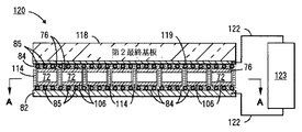
図13は、本願に従って製造される可撓テープ120の一実施形態を示す。図14は図13のA−A線に沿った断面図120である。この構成では、導電素子等の複数の素子72が最終目標基板82と第2の最終目標基板118との間に挟まれる。基板82および118は可撓性があり、導電性かまたは表面導電層をもつ。このテープの作製手順は図12に示す実施形態のものと同じである。
FIG. 13 shows one embodiment of a
この設計では、圧電素子72は均一に分布される。層82および118は例示として示したにすぎず、他の導電材料または表面導電層をもつ材料を使用してもよいことを理解されたい。圧電素子間には、絶縁用として穿孔マイラーもしくはテフロン(登録商標)、または他の導電材等のフィラー114が挿入される。ポリマーテープ118上のメタライゼーション層119はパターニングされていないので、全圧電素子72はすべて接続される。電気コネクタ122が含まれることで、電力および/または制御信号の印加ができる。公知のフィードバックまたはフィードフォワード制御回路123を設けて、圧電素子72の動作を制御する。層82および118は、上述したμm単位以下の導電球85を含む薄い導電エポキシ84による接合工程によって接合されている状態を示す。
In this design, the
フィラー材114の主たる用途は、(第1の)最終基板と第2の最終基板間、またはこれら基板の表面導電層間を電気的に絶縁することである。ただしフィラー材の挿入は任意であることを理解されたい。例えば、各素子の密度が十分高く、たとえ素子間のギャップを充填する材料なしでも(第1の)最終基板と第2の最終基板間またはその表面導電層間が電気短絡する可能性がない程度に素子間のギャップが狭い場合、フィラー材の挿入は行わなくてもよい。また基板の表面導電層がパターニングされて、圧電素子に接合されるべきでない領域に表面導電層がない場合は、フィラー材は使用しなくてもよい場合がある。
The primary use of the
図15は図13のテープの他の実施形態のA−A線に沿った断面図130である。この図は、圧電素子が細長いストリップ134として作成され、フィラー136がこの設計に合う構成になっている様子を示す。この実施形態では、テープ130は一方方向に沿ってのみ可撓性が要求される構造、例えば円筒構造等で使用される能動ファイバー複合材として機能できる。
FIG. 15 is a
図16はA−A線に沿った第3の実施形態の断面図140を示す。この図は、一領域中の圧電素子の密度が可変(すなわち一領域中で素子を均等に分布しなくてもよい)で、圧電素子を様々な形状142に構成できる様子を示す。このため圧電テープの機能を局所的に調整できる。フィラー144は素子の周囲および素子間に分布される。
FIG. 16 shows a
図17はパターニングしたメタライゼーション層152を有するポリマーテープ150を示す。圧電素子の形状および配分、かつ外部回路の設計に応じて、メタライゼーション層をポリマーテープ150上にパターニングして、圧電素子を個々にまたはグループごとに回路線154を介して外部回路に接続でき、圧電素子の数はグループによって異なる。このような回路接続によって、圧電素子をセンサとして、アクチュエータとして、およびトランスデューサとしてそれぞれ同時に使用することが可能になる。従って、圧電テープ自体が検出/検査パネルまたはスキンとなる。
FIG. 17 shows a
図18(A)はA−A線に沿った第4の実施形態の断面図180である。この図は、1つのテープ中に組成の異なる素子(ソフトPZTとハードPZT等)が含まれる、または一部の素子は圧電材料から構成され、他の素子は反強磁性材料や電歪材料等の機能性セラミック材料から構成できる様子を示す。例えば、素子72はある種の圧電材料であり、素子73は他種類の圧電材料または電歪材料である。これら異なる材料は、上述したように異なる基板上に形成され、最終的に1つの最終目標基板上に接合される。これらの素子(異なる材料から形成される)を一緒に接続して1つの外部回路に接続してもよい。しかし好適には、各素子は機能の異なるそれぞれ異なる外部回路に接続する。例えば、テープ190は図18(B)に示すようにパターニングしたメタライゼーション層192を有する。このテープを図18(A)に示す素子を接合する第2の最終目標基板として用いる場合、全素子72が1つのグループとして機能し、別種類の圧電材料または他機能のセラミック材料(反強磁性材料または電歪材料等)からなる素子73は別グループとして機能して、別の外部回路に接続される。
FIG. 18A is a
図19は可撓テープ200を示す。この構成では、複数の素子72および71が最終目標基板82と第2の最終目標基板118との間に挟まれる。基板82および118は可撓性があり、導電性または表面導電層をもつ。この実施形態に示す最終目標基板82は、金属箔等の導電材料または導電層であり、従って他の導電表面層はもたない。最終目標基板118は、金属化したポリマーテープ等の表面導電層119を有する絶縁材である。図13とは異なり、本実施形態の素子72および71は厚さが異なり、上述のように別基板上に作製されるが、最終的には同一基板に接合される。素子72−71間の距離は、第2の最終目標基板(可撓性をもつ)118が両素子72および71に接合可能となるように十分広い。図18(B)に示すポリマーテープ190を第2の最終目標基板として用いて、図19に示す素子の接合を行う場合、素子群72が1つのグループとして機能して1つの外部回路に接続され、素子群71は1つのグループとして機能するため別の外部回路に接続される。
FIG. 19 shows a
図20は、例えば図13のように構成した圧電テープ162,164の2層構造からなる二重圧電テープ160を示す。一実施形態では、表面を金属化した両面ポリマーテープ166を使用して2つの層162,164をつなぐ。この実施形態では、メタライゼーション層167,168および119に個々に参照番号を付す。この実施形態では、これらメタライゼーション層はポリマーテープ166および118の全表面をカバーするが、用途に応じてメタライゼーション層167,168および119は異なる材料から構成してもよく、パターニングし、各層のパターン構成が互いに異なってもよい。本発明の教示に従って多層圧電素子の作製も可能である。
FIG. 20 shows a double
図13〜図20に示すセラミックテープの各種実施形態は、選択的動作が可能な可撓テープであり、各図において代表例として示す各種圧電素子から構成される。 Various embodiments of the ceramic tape shown in FIGS. 13 to 20 are flexible tapes that can be selectively operated, and are composed of various piezoelectric elements shown as typical examples in each drawing.
各材料の特性、例えば弾性係数等がわかれば、周知の計算を用いて中立面が存在するかどうかを判断できる。この情報を本願で使用して圧電材料を平面に対して配置し、圧電素子の感度の増減、またはテープの曲率半径の調整することができる。 If the properties of each material, such as the elastic modulus, are known, it is possible to determine whether or not a neutral plane exists using well-known calculations. This information can be used in this application to position the piezoelectric material relative to a plane to increase or decrease the sensitivity of the piezoelectric element or adjust the radius of curvature of the tape.
以上、本発明を好適な実施形態を参照して説明した。上記の詳細な説明を一読し理解した上で、当業者には各種変形および変更が考えられることは明白である。本発明は、前掲の特許請求の範囲またはその等価物の範囲に含まれる限り、かかる変形および変更をすべて包含するように構成されることを意図する。 The present invention has been described with reference to the preferred embodiments. After reading and understanding the above detailed description, it will be apparent to those skilled in the art that various modifications and changes can be made. The invention is intended to cover all such modifications and alterations insofar as they come within the scope of the appended claims or their equivalents.
72 素子、82 第1導電層、118 第2導電層、120 テープ。 72 elements, 82 first conductive layer, 118 second conductive layer, 120 tape.
Claims (8)
少なくとも部分的に可撓性のある第1の導電層と、
少なくとも部分的に可撓性があり、前記第1の導電層に対向して配置される第2の導電層と、
前記第1の導電層と前記第2の導電層との間に配置され接合されるセンサ、アクチュエータ、またはトランスデューサのうちの少なくとも1つからなる複数の素子と、
前記第1の導電層と前記第2の導電層とに接続し、前記可テープに電力および制御信号を印加する電気接点網とを含むテープ。 Tape
An at least partially flexible first conductive layer;
A second conductive layer that is at least partially flexible and is disposed opposite the first conductive layer;
A plurality of elements consisting of at least one of a sensor, an actuator, and a transducer disposed and joined between the first conductive layer and the second conductive layer;
An electrical contact network connected to the first conductive layer and the second conductive layer and applying power and control signals to the tape.
前記複数のセンサ、アクチュエータ、またはトランスデューサは、分類されグループとして制御されるテープ。 The tape according to claim 1,
A tape in which the plurality of sensors, actuators, or transducers are categorized and controlled as a group.
前記センサ、アクチュエータ、またはトランスデューサのうちの少なくとも1つは、多様な異なる幾何学的形状に形成されるテープ。 The tape according to claim 1,
A tape wherein at least one of said sensor, actuator or transducer is formed in a variety of different geometries.
前記センサ、アクチュエータ、またはトランスデューサのうちの少なくとも1つは、前記センサ、アクチュエータ、またはトランスデューサの密度が不均一となるように前記テープ上に配置された複数のセンサ、アクチュエータ、またはトランスデューサであるテープ。 The tape according to claim 1,
At least one of the sensor, actuator, or transducer is a tape that is a plurality of sensors, actuators, or transducers disposed on the tape such that the sensor, actuator, or transducer has a non-uniform density.
前記第1の導電層および前記第2の導電層の少なくともいずれかは、前記センサ、アクチュエータ、またはトランスデューサのうちの少なくとも1つの形状および分布に対応してパターニングしたメタライゼーション層を有するポリマーテープであるテープ。 The tape according to claim 1,
At least one of the first conductive layer and the second conductive layer is a polymer tape having a metallization layer patterned according to the shape and distribution of at least one of the sensor, actuator, or transducer. tape.
前記センサ、アクチュエータ、またはトランスデューサの少なくとも1つのうち、ある素子は圧電素子を含む1つの機能セラミック材料から構成され、他の素子は1つ以上の他の機能セラミック材料から構成されるテープ。 The tape according to claim 1,
A tape wherein at least one of the sensor, actuator, or transducer is comprised of one functional ceramic material including a piezoelectric element, and the other element is comprised of one or more other functional ceramic materials.
前記複数のアクチュエータ、センサ、またはトランスデューサは、堆積工程によって形成した反強磁性、電歪、または磁歪素子構造を含む複数の他の機能セラミック材料であり、
前記反強磁性またはその他の機能セラミック素子構造の第1の表面上に第1の電極が堆積され、前記反強磁性またはその他の機能セラミック素子構造の第2の表面上に第2の電極が堆積されるテープ。 The tape according to claim 1,
The plurality of actuators, sensors, or transducers are antiferromagnetic, electrostrictive, or other functional ceramic materials including a magnetostrictive element structure formed by a deposition process,
A first electrode is deposited on a first surface of the antiferromagnetic or other functional ceramic element structure, and a second electrode is deposited on a second surface of the antiferromagnetic or other functional ceramic element structure. Tape.
少なくとも1つの第1の基板表面上に材料を堆積して複数の素子構造を形成するステップと、
前記複数の素子構造の各表面上に電極を堆積するステップと、
前記素子構造を第2の基板に接合するステップであって、前記第2の基板は導電性をもつかまたは導電層を有し、かつキャリアプレート上に支持されるステップと、
前記少なくとも1つの第1の基板を前記素子構造から取外すステップと、
第2の側面電極を前記複数の素子構造の第2の表面上に堆積するステップと、
前記素子構造の第2の側面を他の基板に接合するステップであって、前記他の基板は導電性をもつかまたは導電層を有するステップと、
前記キャリアプレートを取外すステップとを含む方法。 A method for producing a tape, comprising:
Depositing material on at least one first substrate surface to form a plurality of device structures;
Depositing an electrode on each surface of the plurality of device structures;
Bonding the device structure to a second substrate, wherein the second substrate has a conductive or conductive layer, and is supported on a carrier plate;
Removing the at least one first substrate from the device structure;
Depositing a second side electrode on a second surface of the plurality of device structures;
Bonding the second side of the device structure to another substrate, wherein the other substrate has conductivity or has a conductive layer;
Removing the carrier plate.
Applications Claiming Priority (2)
| Application Number | Priority Date | Filing Date | Title |
|---|---|---|---|
| US10/376,527 | 2003-02-25 | ||
| US10/376,527 US6964201B2 (en) | 2003-02-25 | 2003-02-25 | Large dimension, flexible piezoelectric ceramic tapes |
Publications (2)
| Publication Number | Publication Date |
|---|---|
| JP2004260176A true JP2004260176A (en) | 2004-09-16 |
| JP4933031B2 JP4933031B2 (en) | 2012-05-16 |
Family
ID=32771496
Family Applications (1)
| Application Number | Title | Priority Date | Filing Date |
|---|---|---|---|
| JP2004045563A Expired - Fee Related JP4933031B2 (en) | 2003-02-25 | 2004-02-23 | Tape and manufacturing method thereof |
Country Status (3)
| Country | Link |
|---|---|
| US (2) | US6964201B2 (en) |
| EP (3) | EP2270865A3 (en) |
| JP (1) | JP4933031B2 (en) |
Cited By (8)
| Publication number | Priority date | Publication date | Assignee | Title |
|---|---|---|---|---|
| JP2008166757A (en) * | 2006-12-29 | 2008-07-17 | Samsung Electro-Mechanics Co Ltd | Manufacturing method of thin film capacitor-incorporating wiring board |
| JP2009232283A (en) * | 2008-03-24 | 2009-10-08 | Panasonic Electric Works Co Ltd | Method of manufacturing baw resonator |
| US7713366B2 (en) | 2005-10-25 | 2010-05-11 | Ngk Insulators, Ltd. | Piezoelectric/electrostrictive film and method for producing the same |
| JP2011066321A (en) * | 2009-09-18 | 2011-03-31 | Tdk Corp | Method of manufacturing thin-film element, thin film element, head gimbal assembly using the thin-film element, and hard disk drive |
| JP2013161970A (en) * | 2012-02-06 | 2013-08-19 | Ngk Insulators Ltd | Manufacturing method of piezoelectric element |
| JP2013168654A (en) * | 2004-12-20 | 2013-08-29 | Palo Alto Research Center Inc | Method for forming ceramic thick film element arrays with fine dimensions, ceramic thick film element arrays with high-definition shapes, and ceramic thick film element arrays with high aspect ratios |
| JP2015119511A (en) * | 2013-12-16 | 2015-06-25 | 株式会社デンソー | Sensor integrated ion conductive polymer actuator and manufacturing method thereof |
| JP2015534667A (en) * | 2012-09-04 | 2015-12-03 | ヨアノイム リサーチ フォルシュングスゲゼルシャフト エムベーハーJoanneum Research Forschungsgesellschaft Mbh | Printed piezoelectric pressure sensing foil |
Families Citing this family (80)
| Publication number | Priority date | Publication date | Assignee | Title |
|---|---|---|---|---|
| US7800199B2 (en) * | 2003-06-24 | 2010-09-21 | Oh Choonsik | Semiconductor circuit |
| FR2802340B1 (en) * | 1999-12-13 | 2003-09-05 | Commissariat Energie Atomique | STRUCTURE COMPRISING PHOTOVOLTAIC CELLS AND METHOD FOR PRODUCING THE SAME |
| KR100510821B1 (en) * | 2003-06-09 | 2005-08-30 | 한국전자통신연구원 | Fabrication method using a temporary substrate of micro structures |
| US7413919B2 (en) | 2003-06-20 | 2008-08-19 | Acellent Technologies, Inc. | Method of manufacturing a structural health monitoring layer |
| US8071438B2 (en) * | 2003-06-24 | 2011-12-06 | Besang Inc. | Semiconductor circuit |
| US20050001201A1 (en) * | 2003-07-03 | 2005-01-06 | Bocko Peter L. | Glass product for use in ultra-thin glass display applications |
| US20060207967A1 (en) * | 2003-07-03 | 2006-09-21 | Bocko Peter L | Porous processing carrier for flexible substrates |
| EP1735586B1 (en) * | 2004-03-03 | 2018-02-14 | Metis Design Corporation | Damage detection device |
| US7351608B1 (en) * | 2004-08-19 | 2008-04-01 | The United States Of America As Represented By The Director Of The National Security Agency | Method of precisely aligning components in flexible integrated circuit module |
| JP4078562B2 (en) * | 2004-08-23 | 2008-04-23 | セイコーエプソン株式会社 | Piezoelectric thin film resonator manufacturing method, piezoelectric thin film resonator, frequency filter, oscillator manufacturing method, oscillator, electronic circuit, and electronic device |
| US7430911B2 (en) * | 2004-08-26 | 2008-10-07 | Acellent Technologies, Inc. | Method of detecting and analyzing changes in the external loading conditions of a structure |
| US7458266B2 (en) * | 2004-09-27 | 2008-12-02 | Samsung Electronics Co. Ltd. | Method and apparatus for detecting a load change upon a structure and analyzing characteristics of resulting damage |
| WO2006041513A1 (en) * | 2004-10-07 | 2006-04-20 | Metis Design Corporation | Sensor infrastructure |
| US7070669B1 (en) | 2004-12-20 | 2006-07-04 | Xerox Corporation | Method for forming ceramic thick film element arrays |
| US7488015B2 (en) * | 2004-12-22 | 2009-02-10 | Bayerische Motoren Werke Aktiengesellschaft | Vehicle systems and methods for detecting pedestrian impacts |
| US8030132B2 (en) * | 2005-05-31 | 2011-10-04 | Semiconductor Energy Laboratory Co., Ltd. | Manufacturing method of semiconductor device including peeling step |
| TWI256082B (en) * | 2005-06-01 | 2006-06-01 | Touch Micro System Tech | Method of segmenting a wafer |
| US20070018083A1 (en) * | 2005-06-13 | 2007-01-25 | Acellent Technologies, Inc. | Structural health monitoring layer having distributed electronics |
| US7387033B2 (en) * | 2005-06-17 | 2008-06-17 | Acellent Technologies, Inc. | Single-wire sensor/actuator network for structure health monitoring |
| WO2008130335A2 (en) * | 2005-06-22 | 2008-10-30 | Reactive Nanotechnologies, Inc. | Reactive composite material structures with electrostatic discharge protection and applications thereof |
| US20070069021A1 (en) * | 2005-09-27 | 2007-03-29 | Palo Alto Research Center Incorporated | Smart floor tiles/carpet for tracking movement in retail, industrial and other environments |
| US7596078B2 (en) * | 2005-11-10 | 2009-09-29 | Acellent Technologies, Inc. | Method and apparatus for reducing crosstalk in a structural health monitoring system |
| US7395189B2 (en) | 2005-11-14 | 2008-07-01 | Acellent Technologies, Inc. | Method and apparatus for switching among elements of a structural health monitoring system |
| US7467857B2 (en) * | 2005-12-20 | 2008-12-23 | Palo Alto Research Center Incorporated | Micromachined fluid ejectors using piezoelectric actuation |
| US7533578B2 (en) * | 2006-04-18 | 2009-05-19 | Metis Design Corporation | Triangulation with co-located sensors |
| KR100734403B1 (en) * | 2006-06-02 | 2007-07-02 | 삼성전기주식회사 | Electro component package and manufacturing method thereof |
| US7764005B2 (en) * | 2006-08-08 | 2010-07-27 | Palo Alto Research Center Incorporated | Traveling wave grids with agitated surface using piezoelectric effect and acoustic traveling waves |
| US20100161283A1 (en) * | 2006-10-03 | 2010-06-24 | Xinlin Qing | Structural health monitoring network |
| US20080155357A1 (en) * | 2006-10-03 | 2008-06-26 | Acellent Technologies, Inc. | Structural health monitoring network |
| US7696676B2 (en) * | 2006-12-18 | 2010-04-13 | Lockheed Martin Corporation | Piezoelectric composite apparatus and related methods |
| US9823833B2 (en) * | 2007-06-05 | 2017-11-21 | Immersion Corporation | Method and apparatus for haptic enabled flexible touch sensitive surface |
| JP5268305B2 (en) * | 2007-08-24 | 2013-08-21 | 株式会社半導体エネルギー研究所 | Method for manufacturing semiconductor device |
| US8201325B2 (en) | 2007-11-22 | 2012-06-19 | International Business Machines Corporation | Method for producing an integrated device |
| WO2010148398A2 (en) * | 2009-06-19 | 2010-12-23 | The Regents Of The University Of Michigan | A thin-film device and method of fabricating the same |
| DE102010005403A1 (en) | 2010-01-22 | 2011-07-28 | Epcos Ag, 81669 | Method for producing a piezoelectric multilayer component and piezoelectric multilayer component |
| JP5399970B2 (en) * | 2010-03-31 | 2014-01-29 | パナソニック株式会社 | Ferroelectric device manufacturing method |
| CN101844130A (en) * | 2010-05-14 | 2010-09-29 | 中国科学技术大学 | Array silicon micro-ultrasonic transducer and manufacturing method thereof |
| JP5463510B2 (en) * | 2010-06-22 | 2014-04-09 | 独立行政法人科学技術振興機構 | Physical quantity sensor and manufacturing method thereof |
| JP5814764B2 (en) * | 2010-12-27 | 2015-11-17 | キヤノン株式会社 | Recording element substrate, recording head, and manufacturing method of recording head |
| EP2489442A1 (en) | 2011-02-18 | 2012-08-22 | Aernnova Engineering Solutions Iberica | Integrated phased array transducer, system and methodology for structural health monitoring of aerospace structures |
| US10238166B2 (en) | 2011-06-28 | 2019-03-26 | Robert Rosenbaum | Instrumented article of fitness and method of determining caloric requirements |
| US10543662B2 (en) | 2012-02-08 | 2020-01-28 | Corning Incorporated | Device modified substrate article and methods for making |
| US10086584B2 (en) | 2012-12-13 | 2018-10-02 | Corning Incorporated | Glass articles and methods for controlled bonding of glass sheets with carriers |
| US10014177B2 (en) | 2012-12-13 | 2018-07-03 | Corning Incorporated | Methods for processing electronic devices |
| US9340443B2 (en) | 2012-12-13 | 2016-05-17 | Corning Incorporated | Bulk annealing of glass sheets |
| TWI617437B (en) | 2012-12-13 | 2018-03-11 | 康寧公司 | Facilitated processing for controlling bonding between sheet and carrier |
| FR3000213B1 (en) * | 2012-12-21 | 2015-05-15 | Eads Europ Aeronautic Defence | RECONFIGURABLE DEVICE FOR CONTROLLING AN ULTRASONIC COMPOSITE STRUCTURE |
| KR20160003031A (en) | 2013-04-26 | 2016-01-08 | 임머숀 코퍼레이션 | Simulation of tangible user interface interactions and gestures using array of haptic cells |
| US9939900B2 (en) | 2013-04-26 | 2018-04-10 | Immersion Corporation | System and method for a haptically-enabled deformable surface |
| US9033227B2 (en) * | 2013-05-20 | 2015-05-19 | Ncr Corporation | Methods and systems for performing security weight checks at checkouts |
| US10510576B2 (en) | 2013-10-14 | 2019-12-17 | Corning Incorporated | Carrier-bonding methods and articles for semiconductor and interposer processing |
| CN106132688B (en) | 2014-01-27 | 2020-07-14 | 康宁股份有限公司 | Article and method for controlled bonding of a sheet to a carrier |
| SG11201608442TA (en) | 2014-04-09 | 2016-11-29 | Corning Inc | Device modified substrate article and methods for making |
| WO2015159628A1 (en) * | 2014-04-18 | 2015-10-22 | 株式会社村田製作所 | Pressure sensor |
| US9690381B2 (en) | 2014-08-21 | 2017-06-27 | Immersion Corporation | Systems and methods for shape input and output for a haptically-enabled deformable surface |
| US9535550B2 (en) | 2014-11-25 | 2017-01-03 | Immersion Corporation | Systems and methods for deformation-based haptic effects |
| EP3297824A1 (en) | 2015-05-19 | 2018-03-28 | Corning Incorporated | Articles and methods for bonding sheets with carriers |
| WO2016209897A1 (en) | 2015-06-26 | 2016-12-29 | Corning Incorporated | Methods and articles including a sheet and a carrier |
| US10985078B2 (en) * | 2015-11-06 | 2021-04-20 | Lam Research Corporation | Sensor and adjuster for a consumable |
| FR3044168A1 (en) * | 2015-11-20 | 2017-05-26 | Crystal Device Tech | GENERATOR BASED ON SOLID PIEZOELECTRIC MATERIAL IN SOFT STRUCTURE |
| US10770646B2 (en) | 2016-03-01 | 2020-09-08 | Qualcomm Incorporated | Manufacturing method for flexible PMUT array |
| TW201825623A (en) | 2016-08-30 | 2018-07-16 | 美商康寧公司 | Siloxane plasma polymers for sheet bonding |
| TWI810161B (en) | 2016-08-31 | 2023-08-01 | 美商康寧公司 | Articles of controllably bonded sheets and methods for making same |
| GB2557894B (en) * | 2016-10-01 | 2019-12-11 | Peratech Holdco Ltd | Flexible sensor |
| US10680161B1 (en) | 2017-03-29 | 2020-06-09 | Apple Inc. | Electronic Devices with Piezoelectric Ink |
| CN106875850A (en) * | 2017-04-18 | 2017-06-20 | 京东方科技集团股份有限公司 | A kind of flexible display screen and its deformation driving method, display device |
| WO2019118660A1 (en) | 2017-12-15 | 2019-06-20 | Corning Incorporated | Method for treating a substrate and method for making articles comprising bonded sheets |
| US10440848B2 (en) | 2017-12-20 | 2019-10-08 | Immersion Corporation | Conformable display with linear actuator |
| CN108039405B (en) * | 2018-01-11 | 2023-10-20 | 中国工程物理研究院总体工程研究所 | Piezoelectric element, piezoelectric sensor, speed and displacement detection device |
| US11638353B2 (en) * | 2018-09-17 | 2023-04-25 | Hutchinson Technology Incorporated | Apparatus and method for forming sensors with integrated electrical circuits on a substrate |
| CN110196125B (en) * | 2019-04-19 | 2020-11-06 | 浙江大学 | Island bridge type flexible sensing array device based on porous structure |
| US11061064B2 (en) * | 2019-05-15 | 2021-07-13 | Nanya Technology Corporation | Semiconductor device and method for detecting cracks |
| CN110265544A (en) * | 2019-06-24 | 2019-09-20 | 京东方科技集团股份有限公司 | Piezoelectric transducer and preparation method, the method and electronic equipment that carry out fingerprint recognition |
| US11231397B2 (en) * | 2019-07-26 | 2022-01-25 | The Boeing Company | Remote wide bandwidth ultrasonic inspection method and apparatus |
| JP7186685B2 (en) * | 2019-09-20 | 2022-12-09 | 株式会社ジャパンディスプレイ | pressure sensor |
| FR3118178B1 (en) | 2020-12-23 | 2023-07-21 | Buerkert Werke Gmbh & Co Kg | Fluid measuring device |
| CN113267289B (en) * | 2021-04-16 | 2022-08-16 | 上海交通大学 | Array type flexible piezoelectric sensor for aircraft engine and preparation method thereof |
| CN113877792B (en) * | 2021-09-27 | 2023-01-13 | 北京信息科技大学 | Large-area flexible piezoelectric transducer based on liquid metal and surface conduction treatment method thereof |
| US20230105781A1 (en) * | 2021-10-01 | 2023-04-06 | Sensitronics, LLC | Low Drift Force Sensor with Capacitive Capability |
| CN114112405B (en) * | 2021-11-23 | 2023-06-20 | 上海交通大学 | Multimode mechanical sensor for aeroengine and preparation method |
Citations (9)
| Publication number | Priority date | Publication date | Assignee | Title |
|---|---|---|---|---|
| JPS6151884A (en) * | 1984-08-22 | 1986-03-14 | Hitachi Ltd | Pressure-sensitive element |
| JPH10125931A (en) * | 1996-08-27 | 1998-05-15 | Seiko Epson Corp | Transfer of thin film element, thin film element, thin film integrated circuit device, active materix substrate and liquid crystal display device |
| JPH10249768A (en) * | 1997-03-12 | 1998-09-22 | Tokai Rubber Ind Ltd | Force sensor |
| WO2000051190A1 (en) * | 1999-02-26 | 2000-08-31 | Active Control Experts, Inc. | Packaged strain actuator |
| JP2000275123A (en) * | 1999-03-25 | 2000-10-06 | Tokai Rubber Ind Ltd | Distribution sensor |
| JP2000337979A (en) * | 1999-05-27 | 2000-12-08 | Tokai Rubber Ind Ltd | Distribution sensor |
| US6335263B1 (en) * | 2000-03-22 | 2002-01-01 | The Regents Of The University Of California | Method of forming a low temperature metal bond for use in the transfer of bulk and thin film materials |
| JP2002102392A (en) * | 2000-08-01 | 2002-04-09 | Head Sport Ag | Racket for ball game sports and production method therefor |
| JP2003019176A (en) * | 2001-07-07 | 2003-01-21 | Hirohide Miwa | Wide-area ultrasonic wave radiator for human body |
Family Cites Families (29)
| Publication number | Priority date | Publication date | Assignee | Title |
|---|---|---|---|---|
| JPS5492307A (en) * | 1977-12-29 | 1979-07-21 | Sony Corp | Driving circuit of electrostrictive converter |
| US4233477A (en) * | 1979-01-31 | 1980-11-11 | The United States Of America As Represented By The Secretary Of The Navy | Flexible, shapeable, composite acoustic transducer |
| US4670682A (en) * | 1984-12-21 | 1987-06-02 | General Electric Company | Piezoelectric ceramic switching devices and systems and method of making the same |
| JPS63150979A (en) | 1986-12-16 | 1988-06-23 | Toshiba Corp | Electric circuit breaker |
| US4906840A (en) * | 1988-01-27 | 1990-03-06 | The Board Of Trustees Of Leland Stanford Jr., University | Integrated scanning tunneling microscope |
| JPH025325A (en) | 1988-06-10 | 1990-01-10 | Fuji Electric Co Ltd | Piezoelectric relay |
| JP2794720B2 (en) * | 1988-08-23 | 1998-09-10 | 松下電器産業株式会社 | Composite piezoelectric vibrator |
| JPH02162782A (en) | 1988-12-15 | 1990-06-22 | Murata Mfg Co Ltd | Driving method for bimorph displacement element |
| DE69026765T2 (en) * | 1989-07-11 | 1996-10-24 | Ngk Insulators Ltd | Piezoelectric / electrostrictive actuator containing a piezoelectric / electrostrictive film |
| US4991283A (en) * | 1989-11-27 | 1991-02-12 | Johnson Gary W | Sensor elements in multilayer ceramic tape structures |
| JPH0423370A (en) | 1990-05-15 | 1992-01-27 | Ube Ind Ltd | Bimorph element |
| DE69223096T2 (en) * | 1991-07-18 | 1998-05-28 | Ngk Insulators Ltd | Piezoelectric / electrostrictive element with a ceramic substrate made of stabilized zirconium dioxide |
| US5869189A (en) * | 1994-04-19 | 1999-02-09 | Massachusetts Institute Of Technology | Composites for structural control |
| US5486494A (en) * | 1994-07-22 | 1996-01-23 | Texas Instruments Incorporated | Method and apparatus for affixing spheres to a conductive sheet |
| US5585136A (en) * | 1995-03-22 | 1996-12-17 | Queen's University At Kingston | Method for producing thick ceramic films by a sol gel coating process |
| US5691960A (en) * | 1995-08-02 | 1997-11-25 | Materials Systems, Inc. | Conformal composite acoustic transducer panel and method of fabrication thereof |
| US6372608B1 (en) * | 1996-08-27 | 2002-04-16 | Seiko Epson Corporation | Separating method, method for transferring thin film device, thin film device, thin film integrated circuit device, and liquid crystal display device manufactured by using the transferring method |
| WO1998024130A1 (en) * | 1996-11-29 | 1998-06-04 | Ngk Insulators, Ltd. | Ceramic element, method of manufacturing ceramic element, display, relay device, and capacitor |
| JP3200026B2 (en) * | 1997-04-04 | 2001-08-20 | 日本碍子株式会社 | Perimeter sensor |
| WO1999000252A1 (en) * | 1997-06-27 | 1999-01-07 | Seiko Epson Corporation | Piezoelectric vibrator unit, method for manufacturing the same, and ink-jet recording head |
| JPH1126834A (en) * | 1997-07-04 | 1999-01-29 | Toshio Fukuda | Pzt thin-film bimorph parallel plate structure and its manufacture |
| US6071795A (en) * | 1998-01-23 | 2000-06-06 | The Regents Of The University Of California | Separation of thin films from transparent substrates by selective optical processing |
| AU3208299A (en) * | 1998-03-26 | 1999-10-18 | Exogen, Inc. | Arrays made from flexible transducer elements |
| US6370964B1 (en) * | 1998-11-23 | 2002-04-16 | The Board Of Trustees Of The Leland Stanford Junior University | Diagnostic layer and methods for detecting structural integrity of composite and metallic materials |
| US6715192B2 (en) * | 1998-12-28 | 2004-04-06 | Ngk Insulators, Ltd. | Method for manufacturing a piezoelectric/electrostrictive device |
| JP2000332313A (en) * | 1999-05-21 | 2000-11-30 | Matsushita Electric Ind Co Ltd | Thin film piezoelectric bimorph element and application thereof |
| JP2001274528A (en) * | 2000-01-21 | 2001-10-05 | Fujitsu Ltd | Inter-substrate transfer method for thin film device |
| JP4387623B2 (en) * | 2000-12-04 | 2009-12-16 | キヤノン株式会社 | Method for manufacturing piezoelectric element |
| US6771007B2 (en) * | 2002-04-17 | 2004-08-03 | The Boeing Company | Vibration induced perpetual energy resource |
-
2003
- 2003-02-25 US US10/376,527 patent/US6964201B2/en not_active Expired - Fee Related
-
2004
- 2004-02-23 JP JP2004045563A patent/JP4933031B2/en not_active Expired - Fee Related
- 2004-02-25 EP EP10179398A patent/EP2270865A3/en not_active Withdrawn
- 2004-02-25 EP EP04004266.5A patent/EP1453103B1/en not_active Expired - Fee Related
- 2004-02-25 EP EP07007909.0A patent/EP1808896B1/en not_active Expired - Fee Related
- 2004-12-20 US US11/017,470 patent/US7118990B1/en not_active Expired - Fee Related
Patent Citations (10)
| Publication number | Priority date | Publication date | Assignee | Title |
|---|---|---|---|---|
| JPS6151884A (en) * | 1984-08-22 | 1986-03-14 | Hitachi Ltd | Pressure-sensitive element |
| JPH10125931A (en) * | 1996-08-27 | 1998-05-15 | Seiko Epson Corp | Transfer of thin film element, thin film element, thin film integrated circuit device, active materix substrate and liquid crystal display device |
| JPH10249768A (en) * | 1997-03-12 | 1998-09-22 | Tokai Rubber Ind Ltd | Force sensor |
| WO2000051190A1 (en) * | 1999-02-26 | 2000-08-31 | Active Control Experts, Inc. | Packaged strain actuator |
| JP2003527046A (en) * | 1999-02-26 | 2003-09-09 | アクティブ コントロール エキスパーツ,インコーポレイテッド | Packaged strain actuator |
| JP2000275123A (en) * | 1999-03-25 | 2000-10-06 | Tokai Rubber Ind Ltd | Distribution sensor |
| JP2000337979A (en) * | 1999-05-27 | 2000-12-08 | Tokai Rubber Ind Ltd | Distribution sensor |
| US6335263B1 (en) * | 2000-03-22 | 2002-01-01 | The Regents Of The University Of California | Method of forming a low temperature metal bond for use in the transfer of bulk and thin film materials |
| JP2002102392A (en) * | 2000-08-01 | 2002-04-09 | Head Sport Ag | Racket for ball game sports and production method therefor |
| JP2003019176A (en) * | 2001-07-07 | 2003-01-21 | Hirohide Miwa | Wide-area ultrasonic wave radiator for human body |
Cited By (10)
| Publication number | Priority date | Publication date | Assignee | Title |
|---|---|---|---|---|
| JP2013168654A (en) * | 2004-12-20 | 2013-08-29 | Palo Alto Research Center Inc | Method for forming ceramic thick film element arrays with fine dimensions, ceramic thick film element arrays with high-definition shapes, and ceramic thick film element arrays with high aspect ratios |
| US7713366B2 (en) | 2005-10-25 | 2010-05-11 | Ngk Insulators, Ltd. | Piezoelectric/electrostrictive film and method for producing the same |
| JP2008166757A (en) * | 2006-12-29 | 2008-07-17 | Samsung Electro-Mechanics Co Ltd | Manufacturing method of thin film capacitor-incorporating wiring board |
| US7845073B2 (en) | 2006-12-29 | 2010-12-07 | Samsung Electro-Mechanics Co., Ltd. | Method of manufacturing circuit board embedding thin film capacitor |
| JP4629088B2 (en) * | 2006-12-29 | 2011-02-09 | サムソン エレクトロ−メカニックス カンパニーリミテッド. | Thin film capacitor built-in wiring board manufacturing method and thin film capacitor built-in wiring board |
| JP2009232283A (en) * | 2008-03-24 | 2009-10-08 | Panasonic Electric Works Co Ltd | Method of manufacturing baw resonator |
| JP2011066321A (en) * | 2009-09-18 | 2011-03-31 | Tdk Corp | Method of manufacturing thin-film element, thin film element, head gimbal assembly using the thin-film element, and hard disk drive |
| JP2013161970A (en) * | 2012-02-06 | 2013-08-19 | Ngk Insulators Ltd | Manufacturing method of piezoelectric element |
| JP2015534667A (en) * | 2012-09-04 | 2015-12-03 | ヨアノイム リサーチ フォルシュングスゲゼルシャフト エムベーハーJoanneum Research Forschungsgesellschaft Mbh | Printed piezoelectric pressure sensing foil |
| JP2015119511A (en) * | 2013-12-16 | 2015-06-25 | 株式会社デンソー | Sensor integrated ion conductive polymer actuator and manufacturing method thereof |
Also Published As
| Publication number | Publication date |
|---|---|
| JP4933031B2 (en) | 2012-05-16 |
| US20060211217A1 (en) | 2006-09-21 |
| EP1808896A1 (en) | 2007-07-18 |
| EP1453103A3 (en) | 2006-04-12 |
| EP1453103A2 (en) | 2004-09-01 |
| US6964201B2 (en) | 2005-11-15 |
| US20040163478A1 (en) | 2004-08-26 |
| US7118990B1 (en) | 2006-10-10 |
| EP1808896B1 (en) | 2017-04-12 |
| EP2270865A3 (en) | 2012-04-18 |
| EP2270865A2 (en) | 2011-01-05 |
| EP1453103B1 (en) | 2013-09-04 |
Similar Documents
| Publication | Publication Date | Title |
|---|---|---|
| JP4933031B2 (en) | Tape and manufacturing method thereof | |
| US7091650B2 (en) | Piezoelectric ceramic thick film element, array of elements, and devices | |
| US20040164649A1 (en) | Bimorph MEMS devices and methods to make same | |
| KR100508222B1 (en) | Mlti-element acoustic probe comprising a common ground electrode | |
| JP4151420B2 (en) | Device manufacturing method | |
| JP5399970B2 (en) | Ferroelectric device manufacturing method | |
| US20030102777A1 (en) | Ultrasonic transducer and method of manufacturing the same | |
| JPH05504740A (en) | Thin film converter inkjet head | |
| KR20160018393A (en) | Device with electrode connected to through wire, and method for manufacturing the same | |
| CN110085127B (en) | Flexible display mother board and flexible display screen manufacturing method | |
| JP4956899B2 (en) | Method for manufacturing thin film piezoelectric element | |
| JP2001509901A (en) | Method of manufacturing acoustic probe | |
| JPH10144974A (en) | Piezoelectric actuator and its manufacturing method | |
| JPH1032454A (en) | Micro piezoelectric vibrator | |
| US20040049901A1 (en) | Method for making a multielement acoustic probe using a metallised and ablated polymer as ground plane | |
| JP2016502758A (en) | Graphene interposer and method for producing the interposer | |
| KR101873640B1 (en) | Method for packaging flexible device and flexible device manufactured by the same | |
| JPH03173652A (en) | Bonding method of piezoelectric element | |
| KR20170108689A (en) | Method for packaging flexible device and flexible device manufactured by the same | |
| JP2006253014A (en) | Pitch changing connector and its manufacturing method | |
| JP2010232456A (en) | Method of manufacturing piezoelectric element, and piezoelectric element | |
| FR2546819A1 (en) | Method for manufacturing electrostatic-printing heads and printing heads obtained by its implementation | |
| JP2011216689A (en) | Method of manufacturing ferroelectric device | |
| JP2017135352A (en) | Through wiring board, manufacturing method of the same, electronic device, and manufacturing method of the same | |
| JPH10209511A (en) | Production of thermoelectric power generating element |
Legal Events
| Date | Code | Title | Description |
|---|---|---|---|
| A621 | Written request for application examination |
Free format text: JAPANESE INTERMEDIATE CODE: A621 Effective date: 20070216 |
|
| A977 | Report on retrieval |
Free format text: JAPANESE INTERMEDIATE CODE: A971007 Effective date: 20101126 |
|
| A131 | Notification of reasons for refusal |
Free format text: JAPANESE INTERMEDIATE CODE: A131 Effective date: 20101207 |
|
| A601 | Written request for extension of time |
Free format text: JAPANESE INTERMEDIATE CODE: A601 Effective date: 20110307 |
|
| A602 | Written permission of extension of time |
Free format text: JAPANESE INTERMEDIATE CODE: A602 Effective date: 20110310 |
|
| A601 | Written request for extension of time |
Free format text: JAPANESE INTERMEDIATE CODE: A601 Effective date: 20110405 |
|
| A602 | Written permission of extension of time |
Free format text: JAPANESE INTERMEDIATE CODE: A602 Effective date: 20110408 |
|
| A601 | Written request for extension of time |
Free format text: JAPANESE INTERMEDIATE CODE: A601 Effective date: 20110427 |
|
| A602 | Written permission of extension of time |
Free format text: JAPANESE INTERMEDIATE CODE: A602 Effective date: 20110506 |
|
| A521 | Request for written amendment filed |
Free format text: JAPANESE INTERMEDIATE CODE: A523 Effective date: 20110602 |
|
| TRDD | Decision of grant or rejection written | ||
| A01 | Written decision to grant a patent or to grant a registration (utility model) |
Free format text: JAPANESE INTERMEDIATE CODE: A01 Effective date: 20120124 |
|
| A01 | Written decision to grant a patent or to grant a registration (utility model) |
Free format text: JAPANESE INTERMEDIATE CODE: A01 |
|
| A61 | First payment of annual fees (during grant procedure) |
Free format text: JAPANESE INTERMEDIATE CODE: A61 Effective date: 20120216 |
|
| R150 | Certificate of patent or registration of utility model |
Free format text: JAPANESE INTERMEDIATE CODE: R150 |
|
| FPAY | Renewal fee payment (event date is renewal date of database) |
Free format text: PAYMENT UNTIL: 20150224 Year of fee payment: 3 |
|
| R250 | Receipt of annual fees |
Free format text: JAPANESE INTERMEDIATE CODE: R250 |
|
| R250 | Receipt of annual fees |
Free format text: JAPANESE INTERMEDIATE CODE: R250 |
|
| R250 | Receipt of annual fees |
Free format text: JAPANESE INTERMEDIATE CODE: R250 |
|
| LAPS | Cancellation because of no payment of annual fees |