JP2013149184A - 表示パネル、駆動回路、駆動方法、および電子機器 - Google Patents
表示パネル、駆動回路、駆動方法、および電子機器 Download PDFInfo
- Publication number
- JP2013149184A JP2013149184A JP2012010743A JP2012010743A JP2013149184A JP 2013149184 A JP2013149184 A JP 2013149184A JP 2012010743 A JP2012010743 A JP 2012010743A JP 2012010743 A JP2012010743 A JP 2012010743A JP 2013149184 A JP2013149184 A JP 2013149184A
- Authority
- JP
- Japan
- Prior art keywords
- drive
- display panel
- unit
- signal
- electrode
- Prior art date
- Legal status (The legal status is an assumption and is not a legal conclusion. Google has not performed a legal analysis and makes no representation as to the accuracy of the status listed.)
- Granted
Links
- 238000000034 method Methods 0.000 title claims description 10
- 238000001514 detection method Methods 0.000 claims abstract description 199
- 239000003990 capacitor Substances 0.000 claims abstract description 16
- 239000004973 liquid crystal related substance Substances 0.000 claims description 51
- 230000007704 transition Effects 0.000 claims description 22
- 230000000630 rising effect Effects 0.000 claims description 8
- 230000007423 decrease Effects 0.000 abstract description 5
- 239000000758 substrate Substances 0.000 description 40
- 230000007274 generation of a signal involved in cell-cell signaling Effects 0.000 description 37
- 238000010586 diagram Methods 0.000 description 19
- 230000004048 modification Effects 0.000 description 16
- 238000012986 modification Methods 0.000 description 16
- 108010020053 Staphylococcus warneri lipase 2 Proteins 0.000 description 7
- 238000006243 chemical reaction Methods 0.000 description 7
- 239000011521 glass Substances 0.000 description 7
- 239000000872 buffer Substances 0.000 description 6
- 230000003071 parasitic effect Effects 0.000 description 6
- 238000005070 sampling Methods 0.000 description 6
- 230000005684 electric field Effects 0.000 description 5
- 238000000605 extraction Methods 0.000 description 5
- 238000004519 manufacturing process Methods 0.000 description 5
- 239000011159 matrix material Substances 0.000 description 4
- 239000010408 film Substances 0.000 description 3
- 102100035954 Choline transporter-like protein 2 Human genes 0.000 description 2
- 101000948115 Homo sapiens Choline transporter-like protein 2 Proteins 0.000 description 2
- 230000009471 action Effects 0.000 description 2
- 229910052782 aluminium Inorganic materials 0.000 description 2
- XAGFODPZIPBFFR-UHFFFAOYSA-N aluminium Chemical compound [Al] XAGFODPZIPBFFR-UHFFFAOYSA-N 0.000 description 2
- 239000003086 colorant Substances 0.000 description 2
- 238000007599 discharging Methods 0.000 description 2
- 230000000694 effects Effects 0.000 description 2
- 238000005401 electroluminescence Methods 0.000 description 2
- 238000005516 engineering process Methods 0.000 description 2
- 239000000284 extract Substances 0.000 description 2
- 230000001151 other effect Effects 0.000 description 2
- 230000004044 response Effects 0.000 description 2
- 238000004904 shortening Methods 0.000 description 2
- 239000010409 thin film Substances 0.000 description 2
- ZOKXTWBITQBERF-UHFFFAOYSA-N Molybdenum Chemical compound [Mo] ZOKXTWBITQBERF-UHFFFAOYSA-N 0.000 description 1
- 230000000295 complement effect Effects 0.000 description 1
- 230000006866 deterioration Effects 0.000 description 1
- 230000005284 excitation Effects 0.000 description 1
- 230000012447 hatching Effects 0.000 description 1
- AMGQUBHHOARCQH-UHFFFAOYSA-N indium;oxotin Chemical compound [In].[Sn]=O AMGQUBHHOARCQH-UHFFFAOYSA-N 0.000 description 1
- 238000009413 insulation Methods 0.000 description 1
- 229910044991 metal oxide Inorganic materials 0.000 description 1
- 150000004706 metal oxides Chemical class 0.000 description 1
- 229910052750 molybdenum Inorganic materials 0.000 description 1
- 239000011733 molybdenum Substances 0.000 description 1
- 230000003287 optical effect Effects 0.000 description 1
- 239000004065 semiconductor Substances 0.000 description 1
- 230000001360 synchronised effect Effects 0.000 description 1
Images


Classifications
-
- G—PHYSICS
- G06—COMPUTING; CALCULATING OR COUNTING
- G06F—ELECTRIC DIGITAL DATA PROCESSING
- G06F3/00—Input arrangements for transferring data to be processed into a form capable of being handled by the computer; Output arrangements for transferring data from processing unit to output unit, e.g. interface arrangements
- G06F3/01—Input arrangements or combined input and output arrangements for interaction between user and computer
- G06F3/03—Arrangements for converting the position or the displacement of a member into a coded form
- G06F3/041—Digitisers, e.g. for touch screens or touch pads, characterised by the transducing means
- G06F3/044—Digitisers, e.g. for touch screens or touch pads, characterised by the transducing means by capacitive means
- G06F3/0445—Digitisers, e.g. for touch screens or touch pads, characterised by the transducing means by capacitive means using two or more layers of sensing electrodes, e.g. using two layers of electrodes separated by a dielectric layer
-
- G—PHYSICS
- G02—OPTICS
- G02F—OPTICAL DEVICES OR ARRANGEMENTS FOR THE CONTROL OF LIGHT BY MODIFICATION OF THE OPTICAL PROPERTIES OF THE MEDIA OF THE ELEMENTS INVOLVED THEREIN; NON-LINEAR OPTICS; FREQUENCY-CHANGING OF LIGHT; OPTICAL LOGIC ELEMENTS; OPTICAL ANALOGUE/DIGITAL CONVERTERS
- G02F1/00—Devices or arrangements for the control of the intensity, colour, phase, polarisation or direction of light arriving from an independent light source, e.g. switching, gating or modulating; Non-linear optics
- G02F1/01—Devices or arrangements for the control of the intensity, colour, phase, polarisation or direction of light arriving from an independent light source, e.g. switching, gating or modulating; Non-linear optics for the control of the intensity, phase, polarisation or colour
- G02F1/13—Devices or arrangements for the control of the intensity, colour, phase, polarisation or direction of light arriving from an independent light source, e.g. switching, gating or modulating; Non-linear optics for the control of the intensity, phase, polarisation or colour based on liquid crystals, e.g. single liquid crystal display cells
- G02F1/133—Constructional arrangements; Operation of liquid crystal cells; Circuit arrangements
- G02F1/1333—Constructional arrangements; Manufacturing methods
- G02F1/13338—Input devices, e.g. touch panels
-
- G—PHYSICS
- G06—COMPUTING; CALCULATING OR COUNTING
- G06F—ELECTRIC DIGITAL DATA PROCESSING
- G06F3/00—Input arrangements for transferring data to be processed into a form capable of being handled by the computer; Output arrangements for transferring data from processing unit to output unit, e.g. interface arrangements
- G06F3/01—Input arrangements or combined input and output arrangements for interaction between user and computer
- G06F3/03—Arrangements for converting the position or the displacement of a member into a coded form
- G06F3/041—Digitisers, e.g. for touch screens or touch pads, characterised by the transducing means
- G06F3/0412—Digitisers structurally integrated in a display
-
- G—PHYSICS
- G06—COMPUTING; CALCULATING OR COUNTING
- G06F—ELECTRIC DIGITAL DATA PROCESSING
- G06F3/00—Input arrangements for transferring data to be processed into a form capable of being handled by the computer; Output arrangements for transferring data from processing unit to output unit, e.g. interface arrangements
- G06F3/01—Input arrangements or combined input and output arrangements for interaction between user and computer
- G06F3/03—Arrangements for converting the position or the displacement of a member into a coded form
- G06F3/041—Digitisers, e.g. for touch screens or touch pads, characterised by the transducing means
- G06F3/0416—Control or interface arrangements specially adapted for digitisers
- G06F3/04166—Details of scanning methods, e.g. sampling time, grouping of sub areas or time sharing with display driving
-
- G—PHYSICS
- G06—COMPUTING; CALCULATING OR COUNTING
- G06F—ELECTRIC DIGITAL DATA PROCESSING
- G06F3/00—Input arrangements for transferring data to be processed into a form capable of being handled by the computer; Output arrangements for transferring data from processing unit to output unit, e.g. interface arrangements
- G06F3/01—Input arrangements or combined input and output arrangements for interaction between user and computer
- G06F3/03—Arrangements for converting the position or the displacement of a member into a coded form
- G06F3/041—Digitisers, e.g. for touch screens or touch pads, characterised by the transducing means
- G06F3/0416—Control or interface arrangements specially adapted for digitisers
- G06F3/0418—Control or interface arrangements specially adapted for digitisers for error correction or compensation, e.g. based on parallax, calibration or alignment
- G06F3/04184—Synchronisation with the driving of the display or the backlighting unit to avoid interferences generated internally
-
- G—PHYSICS
- G06—COMPUTING; CALCULATING OR COUNTING
- G06F—ELECTRIC DIGITAL DATA PROCESSING
- G06F3/00—Input arrangements for transferring data to be processed into a form capable of being handled by the computer; Output arrangements for transferring data from processing unit to output unit, e.g. interface arrangements
- G06F3/01—Input arrangements or combined input and output arrangements for interaction between user and computer
- G06F3/03—Arrangements for converting the position or the displacement of a member into a coded form
- G06F3/041—Digitisers, e.g. for touch screens or touch pads, characterised by the transducing means
- G06F3/044—Digitisers, e.g. for touch screens or touch pads, characterised by the transducing means by capacitive means
- G06F3/0446—Digitisers, e.g. for touch screens or touch pads, characterised by the transducing means by capacitive means using a grid-like structure of electrodes in at least two directions, e.g. using row and column electrodes
-
- G—PHYSICS
- G09—EDUCATION; CRYPTOGRAPHY; DISPLAY; ADVERTISING; SEALS
- G09G—ARRANGEMENTS OR CIRCUITS FOR CONTROL OF INDICATING DEVICES USING STATIC MEANS TO PRESENT VARIABLE INFORMATION
- G09G3/00—Control arrangements or circuits, of interest only in connection with visual indicators other than cathode-ray tubes
- G09G3/20—Control arrangements or circuits, of interest only in connection with visual indicators other than cathode-ray tubes for presentation of an assembly of a number of characters, e.g. a page, by composing the assembly by combination of individual elements arranged in a matrix no fixed position being assigned to or needed to be assigned to the individual characters or partial characters
- G09G3/34—Control arrangements or circuits, of interest only in connection with visual indicators other than cathode-ray tubes for presentation of an assembly of a number of characters, e.g. a page, by composing the assembly by combination of individual elements arranged in a matrix no fixed position being assigned to or needed to be assigned to the individual characters or partial characters by control of light from an independent source
- G09G3/36—Control arrangements or circuits, of interest only in connection with visual indicators other than cathode-ray tubes for presentation of an assembly of a number of characters, e.g. a page, by composing the assembly by combination of individual elements arranged in a matrix no fixed position being assigned to or needed to be assigned to the individual characters or partial characters by control of light from an independent source using liquid crystals
-
- G—PHYSICS
- G06—COMPUTING; CALCULATING OR COUNTING
- G06F—ELECTRIC DIGITAL DATA PROCESSING
- G06F2203/00—Indexing scheme relating to G06F3/00 - G06F3/048
- G06F2203/041—Indexing scheme relating to G06F3/041 - G06F3/045
- G06F2203/04112—Electrode mesh in capacitive digitiser: electrode for touch sensing is formed of a mesh of very fine, normally metallic, interconnected lines that are almost invisible to see. This provides a quite large but transparent electrode surface, without need for ITO or similar transparent conductive material
Landscapes
- Engineering & Computer Science (AREA)
- Theoretical Computer Science (AREA)
- General Engineering & Computer Science (AREA)
- Physics & Mathematics (AREA)
- General Physics & Mathematics (AREA)
- Human Computer Interaction (AREA)
- Nonlinear Science (AREA)
- Crystallography & Structural Chemistry (AREA)
- Chemical & Material Sciences (AREA)
- Optics & Photonics (AREA)
- Mathematical Physics (AREA)
- Computer Hardware Design (AREA)
- Position Input By Displaying (AREA)
- Control Of Indicators Other Than Cathode Ray Tubes (AREA)
- Liquid Crystal (AREA)
- Liquid Crystal Display Device Control (AREA)
Abstract
【解決手段】表示素子と、複数の駆動電極と、各駆動電極との間に静電容量を形成する1または複数のタッチ検出電極と、駆動電極に供給されるパルス部分を含む基本駆動信号を生成する主駆動部と、容量素子を有し、パルス部分に同期して容量素子と駆動電極との間で電荷のやりとりを行う第1の補助駆動部とを備える。
【選択図】図13
Description
1.静電容量式タッチ検出の基本原理
2.第1の実施の形態
3.第2の実施の形態
4.第3の実施の形態
5.適用例
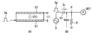
まず最初に、図1〜図3を参照して、本開示の表示パネルにおけるタッチ検出の基本原理について説明する。このタッチ検出方式は、静電容量式のタッチセンサとして具現化されるものであり、例えば図1(A)に示したように、誘電体Dを挟んで互いに対向配置された一対の電極(駆動電極E1およびタッチ検出電極E2)を用い、容量素子を構成する。この構造は、図1(B)に示した等価回路として表される。駆動電極E1、タッチ検出電極E2および誘電体Dによって、容量素子C1が構成される。容量素子C1は、その一端が交流信号源(駆動信号源)Sに接続され、他端Pは抵抗器Rを介して接地されると共に、電圧検出器(タッチ検出回路)DETに接続される。交流信号源Sから駆動電極E1(容量素子C1の一端)に所定の周波数(例えば数kHz〜数十kHz程度)の交流矩形波Sg(図3(B))を印加すると、タッチ検出電極E2(容量素子C1の他端P)に、図3(A)に示したような出力波形(タッチ検出信号Vdet)が現れる。
[構成例]
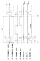
(全体構成例)
図4は、第1の実施の形態に係る表示パネルの一構成例を表すものである。この表示パネル1は、液晶表示デバイスと静電容量式のタッチ検出デバイスとを一体化した、いわゆるインセルタイプの表示パネルである。
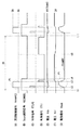
次に、タッチ検出機能付き表示デバイス10の構成例を詳細に説明する。
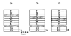
図11は、駆動電極走査部16の一構成例を表すものである。駆動電極走査部16は、走査制御部51と、タッチ検出走査部52と、駆動部530とを備えている。駆動部530は、20個の駆動部53(1)〜53(20)を有している。以後、20個の駆動部53(2)〜53(20)のうちの任意の一つをさす場合には、単に駆動部53を用いるものとする。
補助駆動部18の説明に先立ち、まず、表示パネル1における各ブロックの配置について説明する。
続いて、本実施の形態の表示パネル1の動作および作用について説明する。
まず、図4を参照して、表示パネル1の全体動作概要を説明する。制御部11は、映像信号Vdispに基づいて、ゲートドライバ12、ソースドライバ13、駆動信号生成部15、駆動電極走査部16、補助駆動部18、およびタッチ検出部40に対してそれぞれ制御信号を供給し、これらがお互いに同期して動作するように制御する。
(詳細動作)
次に、表示パネル1の詳細動作を説明する。
次に、補助駆動部18の動作について、詳細に説明する。
以上のように本実施の形態では、補助駆動部を設けたので、駆動信号の遷移時間を短くすることができ、各駆動電極ブロックをより短い時間で駆動することができる。
上記実施の形態では、容量素子CH,CLの電極61を画素電極22と同じ層により形成し、電極62を駆動電極COMLと同じ層により形成したが、これに限定されるものではなく、これに代えて、例えば、図19(A),(B)に示すように形成してもよい。以下、容量素子CHを例に説明する。
上記実施の形態では、制御部11は、図17に示したように、交流駆動信号VcomACが低レベルから高レベルに変化するタイミングt2において、制御信号CTLHを低レベルから高レベルに変化させ、交流駆動信号VcomACが高レベルから低レベルに変化するタイミングt3において、制御信号CTLLを低レベルから高レベルに変化させたが、これに限定するものではなく、これに代えて、例えば、図20に示したように、タイミングt2よりも前に制御信号CTLHを低レベルから高レベルに変化させ、タイミングt3よりも前に制御信号CTLLを低レベルから高レベルに変化させてもよい。
次に、第2の実施の形態に係る表示パネル7について説明する。本実施の形態は、補助駆動部の容量素子CH,CLを、専用の配線を介して初期化するように構成したものである。なお、上記第1の実施の形態に係る表示パネル1と実質的に同一の構成部分には同一の符号を付し、適宜説明を省略する。
上記実施の形態に係る表示パネル7に、上記第1の実施の形態の変形例1−1,1−2を適用してもよい。
上記実施の形態では、直流信号Vch1の電圧を交流駆動信号VcomAC2の高レベル電圧(電圧VH)と同じにし、直流信号Vcl1の電圧を交流駆動信号VcomAC2の低レベル電圧(0V)と同じにしたが、これに限定されるものではなく、これらの電圧は任意に設定可能である。具体的には、例えば、直流信号Vch1の電圧を電圧VHよりも高い電圧に設定し、直流信号Vcl1の電圧を0Vよりも低い電圧に設定してもよい。
次に、第3の実施の形態に係る表示パネル8について説明する。本実施の形態は、第2の実施の形態に係る補助駆動部78において、配線LHと容量素子CHとの間にスイッチを設け、同様に、配線LLと容量素子CLとの間にスイッチを設けたものである。なお、上記第2の実施の形態に係る表示パネル7と実質的に同一の構成部分には同一の符号を付し、適宜説明を省略する。
上記実施の形態では、直流信号Vch1の電圧を電圧VHより高い電圧VH2にし、直流信号Vcl1の電圧を0Vより低電圧VL2にしたが、これに限定されるものではなく、これに代えて、例えば、直流信号Vch1の電圧を電圧VHにし、直流信号Vcl1の電圧を0Vにしてもよい。
次に、上記実施の形態および変形例で説明した表示パネルの適用例について説明する。
複数の駆動電極と、
各駆動電極との間に静電容量を形成する1または複数のタッチ検出電極と、
前記駆動電極に供給されるパルス部分を含む基本駆動信号を生成する主駆動部と、
容量素子を有し、前記パルス部分に同期して前記容量素子と前記駆動電極との間で電荷のやりとりを行う第1の補助駆動部と
を備えた表示パネル。
前記パルス部分は、2つの電圧レベルの間で遷移するものであり、
前記第1のスイッチは、前記パルス部分における立ち上がりまたは立ち下がりに対応するタイミングでオン状態になる
前記(1)に記載の表示パネル。
前記容量素子は、前記第1のスイッチがオフ状態である期間において、前記第2レベルの電圧に対応して予め定められた第3レベルの電圧になるように設定される
前記(2)に記載の表示パネル。
前記第1のスイッチは、前記基本駆動信号に前記直流部分が現れる期間にもオン状態になる
前記(3)に記載の表示パネル。
前記(3)に記載の表示パネル。
前記第1の補助駆動部は、前記電圧生成部が生成した前記第3レベルの電圧の前記容量素子への供給を制御する電圧供給スイッチをさらに有する
前記(3)に記載の表示パネル。
前記(6)に記載の表示パネル。
前記(3)から(7)のいずれかに記載の表示パネル。
前記第2レベルの電圧が前記第1レベルの電圧よりも大きい場合には、前記第2レベルの電圧よりも大きく、
前記第2レベルの電圧が前記第1レベルの電圧よりも小さい場合には、前記第2レベルの電圧よりも小さい
前記(3)から(7)のいずれかに記載の表示パネル。
前記(2)から(9)のいずれかに記載の表示パネル。
前記主駆動部は、前記複数の駆動電極のうち、一方の最端位置に配置された駆動電極の近傍に配置され、
前記第1の補助駆動部は、他方の最端位置に配置された駆動電極の近傍に配置されている
前記(1)から(10)のいずれかに記載の表示パネル。
前記容量素子の容量値は、前記所定数の駆動電極の容量値の10倍以下である
前記(1)から(11)のいずれかに記載の表示パネル。
前記第2のスイッチは、前記パルス部分の立ち上がりタイミングおよび立ち下がりタイミングのうち、前記第1のスイッチがオンになるタイミングとは逆のタイミングでオン状態になる
前記(1)から(12)のいずれかに記載の表示パネル。
液晶層と、
前記液晶層と前記駆動電極との間に形成され、もしくは前記駆動電極を挟んで前記液晶層と対向するように配置された画素電極と
を含む
前記(1)から(13)のいずれかに記載の表示パネル。
前記(14)に記載の表示パネル。
前記容量素子は、前記画素トランジスタのゲート電極と同層の電極を含む
前記(14)または(15)に記載の表示パネル。
液晶層と、
前記液晶層を挟んで前記駆動電極と対向するように配置された画素電極と
を含む
前記(1)から(13)のいずれかに記載の表示パネル。
駆動回路。
駆動方法。
前記表示パネルを利用した動作制御を行う制御部と
を備え、
前記表示パネルは、
表示素子と、
複数の駆動電極と、
各駆動電極との間に静電容量を形成する1または複数のタッチ検出電極と、
前記駆動電極に供給されるパルス部分を含む基本駆動信号を生成する主駆動部と、
容量素子を有し、前記パルス部分に同期して、前記容量素子と駆動電極との間で電荷のやりとりを行う第1の補助駆動部と
を有する
電子機器。
Claims (20)
- 表示素子と、
複数の駆動電極と、
各駆動電極との間に静電容量を形成する1または複数のタッチ検出電極と、
前記駆動電極に供給されるパルス部分を含む基本駆動信号を生成する主駆動部と、
容量素子を有し、前記パルス部分に同期して前記容量素子と前記駆動電極との間で電荷のやりとりを行う第1の補助駆動部と
を備えた表示パネル。 - 前記第1の補助駆動部は、前記容量素子と前記駆動電極との間の電荷のやりとりを制御する第1のスイッチをさらに有し、
前記パルス部分は、2つの電圧レベルの間で遷移するものであり、
前記第1のスイッチは、前記パルス部分における立ち上がりまたは立ち下がりに対応するタイミングでオン状態になる
請求項1に記載の表示パネル。 - 前記パルス部分は、第1レベルの電圧から第2レベルの電圧に遷移し、
前記容量素子は、前記第1のスイッチがオフ状態である期間において、前記第2レベルの電圧に対応して予め定められた第3レベルの電圧になるように設定される
請求項2に記載の表示パネル。 - 前記基本駆動信号は、前記パルス部分が現れる期間とは異なる期間において前記第3レベルの電圧に保たれる直流部分を含み、
前記第1のスイッチは、前記基本駆動信号に前記直流部分が現れる期間にもオン状態になる
請求項3に記載の表示パネル。 - 前記第3レベルの電圧を生成して前記容量素子に供給する電圧供給部をさらに有する
請求項3に記載の表示パネル。 - 前記第3レベルの電圧を生成する電圧生成部をさらに有し、
前記第1の補助駆動部は、前記電圧生成部が生成した前記第3レベルの電圧の前記容量素子への供給を制御する電圧供給スイッチをさらに有する
請求項3に記載の表示パネル。 - 前記電圧供給スイッチは、前記第1のスイッチがオフ状態である期間においてオン状態になる
請求項6に記載の表示パネル。 - 前記第3レベルの電圧は、前記第2レベルの電圧と同じ電圧レベルである
請求項3に記載の表示パネル。 - 前記第3レベルの電圧は、
前記第2レベルの電圧が前記第1レベルの電圧よりも大きい場合には、前記第2レベルの電圧よりも大きく、
前記第2レベルの電圧が前記第1レベルの電圧よりも小さい場合には、前記第2レベルの電圧よりも小さい
請求項3に記載の表示パネル。 - 前記第1のスイッチは、前記パルス部分における立ち上がりと同時もしくはその直前、または立ち下がりと同時もしくはその直前でオン状態になる
請求項2に記載の表示パネル。 - 前記複数の駆動電極は、所定の方向に延伸するようにそれぞれ形成されるとともに、前記所定の方向と直交する方向に配列され、
前記主駆動部は、前記複数の駆動電極のうち、一方の最端位置に配置された駆動電極の近傍に配置され、
前記第1の補助駆動部は、他方の最端位置に配置された駆動電極の近傍に配置されている
請求項1に記載の表示パネル。 - 前記基本駆動信号のうちのパルス部分を、前記複数の駆動電極に対して、所定数の駆動電極ずつ切り換えて供給する走査部をさらに備え、
前記容量素子の容量値は、前記所定数の駆動電極の容量値の10倍以下である
請求項1に記載の表示パネル。 - 容量素子と、その容量素子と前記駆動電極との間の電荷のやりとりを制御する第2のスイッチとを有する第2の補助駆動部をさらに備え、
前記第2のスイッチは、前記パルス部分の立ち上がりタイミングおよび立ち下がりタイミングのうち、前記第1のスイッチがオンになるタイミングとは逆のタイミングでオン状態になる
請求項1に記載の表示パネル。 - 前記表示素子は、
液晶層と、
前記液晶層と前記駆動電極との間に形成され、もしくは前記駆動電極を挟んで前記液晶層と対向するように配置された画素電極と
を含む
請求項1に記載の表示パネル。 - 前記容量素子は、前記駆動電極と同層の電極と、前記画素電極と同層の電極とを含む
請求項14に記載の表示パネル。 - 前記表示素子は、さらに画素トランジスタを含み、
前記容量素子は、前記画素トランジスタのゲート電極と同層の電極を含む
請求項14に記載の表示パネル。 - 前記表示素子は、
液晶層と、
前記液晶層を挟んで前記駆動電極と対向するように配置された画素電極と
を含む
請求項1に記載の表示パネル。 - 容量素子を有し、基本駆動信号のうちの、駆動電極に供給されるパルス部分に同期して、前記容量素子と前記駆動電極との間で電荷のやりとりを行う
駆動回路。 - 駆動電極に基本駆動信号のパルス部分を供給するとともに、前記パルス部分に同期して、容量素子と前記駆動電極との間で電荷のやりとりを行う
駆動方法。 - 表示パネルと、
前記表示パネルを利用した動作制御を行う制御部と
を備え、
前記表示パネルは、
表示素子と、
複数の駆動電極と、
各駆動電極との間に静電容量を形成する1または複数のタッチ検出電極と、
前記駆動電極に供給されるパルス部分を含む基本駆動信号を生成する主駆動部と、
容量素子を有し、前記パルス部分に同期して、前記容量素子と駆動電極との間で電荷のやりとりを行う第1の補助駆動部と
を有する
電子機器。
Priority Applications (6)
| Application Number | Priority Date | Filing Date | Title |
|---|---|---|---|
| JP2012010743A JP5840510B2 (ja) | 2012-01-23 | 2012-01-23 | 表示パネルおよび表示パネルの駆動方法 |
| TW101142521A TWI506489B (zh) | 2012-01-23 | 2012-11-14 | 顯示器面板,驅動器電路,驅動方法,及電子裝置 |
| US13/718,634 US9030431B2 (en) | 2012-01-23 | 2012-12-18 | Display panel and apparatus with capacitive element in auxiliary driver |
| KR1020130004287A KR102036927B1 (ko) | 2012-01-23 | 2013-01-15 | 디스플레이 패널, 드라이버 회로, 구동 방법, 및 전자 장치 |
| CN201310016220.9A CN103218091B (zh) | 2012-01-23 | 2013-01-16 | 显示面板、驱动电路、驱动方法以及电子设备 |
| US14/678,281 US9430086B2 (en) | 2012-01-23 | 2015-04-03 | Display panel, driver circuit, driving method, and electronic apparatus |
Applications Claiming Priority (1)
| Application Number | Priority Date | Filing Date | Title |
|---|---|---|---|
| JP2012010743A JP5840510B2 (ja) | 2012-01-23 | 2012-01-23 | 表示パネルおよび表示パネルの駆動方法 |
Publications (2)
| Publication Number | Publication Date |
|---|---|
| JP2013149184A true JP2013149184A (ja) | 2013-08-01 |
| JP5840510B2 JP5840510B2 (ja) | 2016-01-06 |
Family
ID=48796829
Family Applications (1)
| Application Number | Title | Priority Date | Filing Date |
|---|---|---|---|
| JP2012010743A Active JP5840510B2 (ja) | 2012-01-23 | 2012-01-23 | 表示パネルおよび表示パネルの駆動方法 |
Country Status (5)
| Country | Link |
|---|---|
| US (2) | US9030431B2 (ja) |
| JP (1) | JP5840510B2 (ja) |
| KR (1) | KR102036927B1 (ja) |
| CN (1) | CN103218091B (ja) |
| TW (1) | TWI506489B (ja) |
Cited By (1)
| Publication number | Priority date | Publication date | Assignee | Title |
|---|---|---|---|---|
| WO2016084725A1 (ja) * | 2014-11-28 | 2016-06-02 | シャープ株式会社 | 位置入力機能付き表示装置 |
Families Citing this family (14)
| Publication number | Priority date | Publication date | Assignee | Title |
|---|---|---|---|---|
| JP6027903B2 (ja) * | 2013-01-30 | 2016-11-16 | シナプティクス・ジャパン合同会社 | 半導体装置 |
| CN103336645B (zh) * | 2013-06-24 | 2017-04-12 | 敦泰科技有限公司 | 电容式触控设备及其检测系统 |
| JP6121812B2 (ja) * | 2013-06-25 | 2017-04-26 | 株式会社ジャパンディスプレイ | タッチパネル付液晶表示装置 |
| JP6250342B2 (ja) * | 2013-09-20 | 2017-12-20 | 株式会社ジャパンディスプレイ | 表示装置 |
| KR101641690B1 (ko) * | 2013-09-25 | 2016-07-21 | 엘지디스플레이 주식회사 | 터치스크린 일체형 표시장치 |
| US11221706B2 (en) | 2013-09-27 | 2022-01-11 | Sensel, Inc. | Tactile touch sensor system and method |
| CA2925692C (en) | 2013-09-27 | 2021-09-21 | Sensel, Inc. | Touch sensor detector system and method |
| WO2015126848A1 (en) * | 2014-02-18 | 2015-08-27 | Arokia Nathan | Dynamic switching of power modes for touch screens using force touch |
| JP6486692B2 (ja) | 2015-01-09 | 2019-03-20 | 株式会社ジャパンディスプレイ | 液晶表示装置 |
| CN105116588A (zh) * | 2015-09-23 | 2015-12-02 | 深圳市华星光电技术有限公司 | 触控面板及液晶显示器 |
| CN106468982B (zh) * | 2016-08-31 | 2019-03-01 | 北京集创北方科技股份有限公司 | 触摸显示控制装置和方法 |
| KR102500291B1 (ko) * | 2016-09-05 | 2023-02-16 | 삼성전자주식회사 | 통신 인터페이스 장치 및 디스플레이 장치 |
| US11528028B2 (en) * | 2020-01-05 | 2022-12-13 | Brilliant Home Technology, Inc. | Touch-based control device to detect touch input without blind spots |
| US11353988B1 (en) * | 2021-02-19 | 2022-06-07 | Himax Technologies Limited | Touch display apparatus and method for touch display panel |
Citations (5)
| Publication number | Priority date | Publication date | Assignee | Title |
|---|---|---|---|---|
| JPH08123370A (ja) * | 1994-10-24 | 1996-05-17 | Fujitsu Ltd | 断線救済回路及びそれを用いた表示装置 |
| JP2008009368A (ja) * | 2006-06-29 | 2008-01-17 | Lg Phillips Lcd Co Ltd | 液晶表示装置及びその駆動方法 |
| JP2009258182A (ja) * | 2008-04-11 | 2009-11-05 | Sony Corp | 表示装置とその駆動方法 |
| JP2011233018A (ja) * | 2010-04-28 | 2011-11-17 | Sony Corp | タッチ検出機能付き表示装置、駆動方法、および電子機器 |
| JP2012008910A (ja) * | 2010-06-28 | 2012-01-12 | Casio Comput Co Ltd | 位置入力装置 |
Family Cites Families (8)
| Publication number | Priority date | Publication date | Assignee | Title |
|---|---|---|---|---|
| US6970160B2 (en) | 2002-12-19 | 2005-11-29 | 3M Innovative Properties Company | Lattice touch-sensing system |
| TW201007538A (en) * | 2008-08-15 | 2010-02-16 | Elan Microelectronics | Touch sensor driving method and device and capacitive touch module |
| US20110068810A1 (en) * | 2009-04-03 | 2011-03-24 | Tpo Displays Corp. | Sensing method and driving circuit of capacitive touch screen |
| JP5191452B2 (ja) * | 2009-06-29 | 2013-05-08 | 株式会社ジャパンディスプレイウェスト | タッチパネルの駆動方法、静電容量型タッチパネルおよびタッチ検出機能付き表示装置 |
| US8947392B2 (en) * | 2009-12-11 | 2015-02-03 | Multek Display (Hong Kong) Limited | Multi-driver touch panel |
| JP5117633B2 (ja) * | 2010-02-25 | 2013-01-16 | シャープ株式会社 | 液晶表示装置 |
| JP5382658B2 (ja) * | 2010-02-26 | 2014-01-08 | 株式会社ジャパンディスプレイ | タッチセンサ付き表示装置、タッチパネル、タッチパネルの駆動方法、および電子機器 |
| TWI436257B (zh) * | 2010-03-09 | 2014-05-01 | Innolux Corp | 表面電容式觸控面板及其顯示裝置與電子裝置及驅動方法 |
-
2012
- 2012-01-23 JP JP2012010743A patent/JP5840510B2/ja active Active
- 2012-11-14 TW TW101142521A patent/TWI506489B/zh not_active IP Right Cessation
- 2012-12-18 US US13/718,634 patent/US9030431B2/en not_active Expired - Fee Related
-
2013
- 2013-01-15 KR KR1020130004287A patent/KR102036927B1/ko active IP Right Grant
- 2013-01-16 CN CN201310016220.9A patent/CN103218091B/zh active Active
-
2015
- 2015-04-03 US US14/678,281 patent/US9430086B2/en active Active
Patent Citations (5)
| Publication number | Priority date | Publication date | Assignee | Title |
|---|---|---|---|---|
| JPH08123370A (ja) * | 1994-10-24 | 1996-05-17 | Fujitsu Ltd | 断線救済回路及びそれを用いた表示装置 |
| JP2008009368A (ja) * | 2006-06-29 | 2008-01-17 | Lg Phillips Lcd Co Ltd | 液晶表示装置及びその駆動方法 |
| JP2009258182A (ja) * | 2008-04-11 | 2009-11-05 | Sony Corp | 表示装置とその駆動方法 |
| JP2011233018A (ja) * | 2010-04-28 | 2011-11-17 | Sony Corp | タッチ検出機能付き表示装置、駆動方法、および電子機器 |
| JP2012008910A (ja) * | 2010-06-28 | 2012-01-12 | Casio Comput Co Ltd | 位置入力装置 |
Cited By (3)
| Publication number | Priority date | Publication date | Assignee | Title |
|---|---|---|---|---|
| WO2016084725A1 (ja) * | 2014-11-28 | 2016-06-02 | シャープ株式会社 | 位置入力機能付き表示装置 |
| JPWO2016084725A1 (ja) * | 2014-11-28 | 2017-08-31 | シャープ株式会社 | 位置入力機能付き表示装置 |
| US10386964B2 (en) | 2014-11-28 | 2019-08-20 | Sharp Kabushiki Kaisha | Display device fitted with position input function |
Also Published As
| Publication number | Publication date |
|---|---|
| US9030431B2 (en) | 2015-05-12 |
| CN103218091B (zh) | 2017-06-09 |
| US20150212645A1 (en) | 2015-07-30 |
| JP5840510B2 (ja) | 2016-01-06 |
| TW201331802A (zh) | 2013-08-01 |
| US20130187887A1 (en) | 2013-07-25 |
| CN103218091A (zh) | 2013-07-24 |
| KR102036927B1 (ko) | 2019-10-25 |
| TWI506489B (zh) | 2015-11-01 |
| US9430086B2 (en) | 2016-08-30 |
| KR20130086165A (ko) | 2013-07-31 |
Similar Documents
| Publication | Publication Date | Title |
|---|---|---|
| JP5840510B2 (ja) | 表示パネルおよび表示パネルの駆動方法 | |
| US11650685B2 (en) | Display panel with touch detection function, method of driving the same, driving circuit, and electronic unit | |
| JP5710449B2 (ja) | 表示装置、駆動回路、駆動方法、および電子機器 | |
| JP5685132B2 (ja) | タッチ検出機能付き表示パネル、駆動回路、および電子機器 | |
| JP5726606B2 (ja) | タッチ検出機能付き表示パネルおよびその駆動方法、駆動回路、ならびに電子機器 | |
| JP5539106B2 (ja) | タッチ検出機能付き表示装置、駆動回路、タッチ検出機能付き表示装置の駆動方法、および電子機器 | |
| US8791916B2 (en) | Display panel with touch detection function, method of driving the same, driving circuit, and electronic unit | |
| JP5980157B2 (ja) | タッチ検出機能付き表示装置及び電子機器 | |
| JP5685512B2 (ja) | 表示装置、タッチ検出装置、駆動方法、および電子機器 | |
| JP5788766B2 (ja) | タッチ検出機能付き表示パネルおよびその駆動方法、駆動回路、ならびに電子機器 | |
| JP5909296B2 (ja) | タッチ検出機能付き表示パネルおよびその駆動方法、駆動回路、ならびに電子機器 |
Legal Events
| Date | Code | Title | Description |
|---|---|---|---|
| A621 | Written request for application examination |
Free format text: JAPANESE INTERMEDIATE CODE: A621 Effective date: 20140512 |
|
| A711 | Notification of change in applicant |
Free format text: JAPANESE INTERMEDIATE CODE: A712 Effective date: 20140512 |
|
| A977 | Report on retrieval |
Free format text: JAPANESE INTERMEDIATE CODE: A971007 Effective date: 20150225 |
|
| A131 | Notification of reasons for refusal |
Free format text: JAPANESE INTERMEDIATE CODE: A131 Effective date: 20150331 |
|
| A521 | Request for written amendment filed |
Free format text: JAPANESE INTERMEDIATE CODE: A523 Effective date: 20150526 |
|
| TRDD | Decision of grant or rejection written | ||
| A01 | Written decision to grant a patent or to grant a registration (utility model) |
Free format text: JAPANESE INTERMEDIATE CODE: A01 Effective date: 20151027 |
|
| A61 | First payment of annual fees (during grant procedure) |
Free format text: JAPANESE INTERMEDIATE CODE: A61 Effective date: 20151111 |
|
| R150 | Certificate of patent or registration of utility model |
Ref document number: 5840510 Country of ref document: JP Free format text: JAPANESE INTERMEDIATE CODE: R150 |
|
| R250 | Receipt of annual fees |
Free format text: JAPANESE INTERMEDIATE CODE: R250 |
|
| R250 | Receipt of annual fees |
Free format text: JAPANESE INTERMEDIATE CODE: R250 |
|
| R250 | Receipt of annual fees |
Free format text: JAPANESE INTERMEDIATE CODE: R250 |
|
| R250 | Receipt of annual fees |
Free format text: JAPANESE INTERMEDIATE CODE: R250 |
|
| R250 | Receipt of annual fees |
Free format text: JAPANESE INTERMEDIATE CODE: R250 |
|
| R250 | Receipt of annual fees |
Free format text: JAPANESE INTERMEDIATE CODE: R250 |