JP2013145799A - Laser diode and method of manufacturing laser diode - Google Patents
Laser diode and method of manufacturing laser diode Download PDFInfo
- Publication number
- JP2013145799A JP2013145799A JP2012005367A JP2012005367A JP2013145799A JP 2013145799 A JP2013145799 A JP 2013145799A JP 2012005367 A JP2012005367 A JP 2012005367A JP 2012005367 A JP2012005367 A JP 2012005367A JP 2013145799 A JP2013145799 A JP 2013145799A
- Authority
- JP
- Japan
- Prior art keywords
- degrees
- plane
- semipolar
- semiconductor
- optical waveguide
- Prior art date
- Legal status (The legal status is an assumption and is not a legal conclusion. Google has not performed a legal analysis and makes no representation as to the accuracy of the status listed.)
- Pending
Links
Images


Classifications
-
- H—ELECTRICITY
- H01—ELECTRIC ELEMENTS
- H01S—DEVICES USING THE PROCESS OF LIGHT AMPLIFICATION BY STIMULATED EMISSION OF RADIATION [LASER] TO AMPLIFY OR GENERATE LIGHT; DEVICES USING STIMULATED EMISSION OF ELECTROMAGNETIC RADIATION IN WAVE RANGES OTHER THAN OPTICAL
- H01S5/00—Semiconductor lasers
- H01S5/30—Structure or shape of the active region; Materials used for the active region
- H01S5/3013—AIIIBV compounds
-
- B—PERFORMING OPERATIONS; TRANSPORTING
- B82—NANOTECHNOLOGY
- B82Y—SPECIFIC USES OR APPLICATIONS OF NANOSTRUCTURES; MEASUREMENT OR ANALYSIS OF NANOSTRUCTURES; MANUFACTURE OR TREATMENT OF NANOSTRUCTURES
- B82Y20/00—Nanooptics, e.g. quantum optics or photonic crystals
-
- H—ELECTRICITY
- H01—ELECTRIC ELEMENTS
- H01S—DEVICES USING THE PROCESS OF LIGHT AMPLIFICATION BY STIMULATED EMISSION OF RADIATION [LASER] TO AMPLIFY OR GENERATE LIGHT; DEVICES USING STIMULATED EMISSION OF ELECTROMAGNETIC RADIATION IN WAVE RANGES OTHER THAN OPTICAL
- H01S5/00—Semiconductor lasers
- H01S5/30—Structure or shape of the active region; Materials used for the active region
- H01S5/32—Structure or shape of the active region; Materials used for the active region comprising PN junctions, e.g. hetero- or double- heterostructures
- H01S5/3202—Structure or shape of the active region; Materials used for the active region comprising PN junctions, e.g. hetero- or double- heterostructures grown on specifically orientated substrates, or using orientation dependent growth
- H01S5/320275—Structure or shape of the active region; Materials used for the active region comprising PN junctions, e.g. hetero- or double- heterostructures grown on specifically orientated substrates, or using orientation dependent growth semi-polar orientation
-
- H—ELECTRICITY
- H01—ELECTRIC ELEMENTS
- H01S—DEVICES USING THE PROCESS OF LIGHT AMPLIFICATION BY STIMULATED EMISSION OF RADIATION [LASER] TO AMPLIFY OR GENERATE LIGHT; DEVICES USING STIMULATED EMISSION OF ELECTROMAGNETIC RADIATION IN WAVE RANGES OTHER THAN OPTICAL
- H01S5/00—Semiconductor lasers
- H01S5/30—Structure or shape of the active region; Materials used for the active region
- H01S5/34—Structure or shape of the active region; Materials used for the active region comprising quantum well or superlattice structures, e.g. single quantum well [SQW] lasers, multiple quantum well [MQW] lasers or graded index separate confinement heterostructure [GRINSCH] lasers
- H01S5/343—Structure or shape of the active region; Materials used for the active region comprising quantum well or superlattice structures, e.g. single quantum well [SQW] lasers, multiple quantum well [MQW] lasers or graded index separate confinement heterostructure [GRINSCH] lasers in AIIIBV compounds, e.g. AlGaAs-laser, InP-based laser
- H01S5/34333—Structure or shape of the active region; Materials used for the active region comprising quantum well or superlattice structures, e.g. single quantum well [SQW] lasers, multiple quantum well [MQW] lasers or graded index separate confinement heterostructure [GRINSCH] lasers in AIIIBV compounds, e.g. AlGaAs-laser, InP-based laser with a well layer based on Ga(In)N or Ga(In)P, e.g. blue laser
-
- H—ELECTRICITY
- H01—ELECTRIC ELEMENTS
- H01S—DEVICES USING THE PROCESS OF LIGHT AMPLIFICATION BY STIMULATED EMISSION OF RADIATION [LASER] TO AMPLIFY OR GENERATE LIGHT; DEVICES USING STIMULATED EMISSION OF ELECTROMAGNETIC RADIATION IN WAVE RANGES OTHER THAN OPTICAL
- H01S5/00—Semiconductor lasers
- H01S5/0014—Measuring characteristics or properties thereof
- H01S5/0035—Simulations of laser characteristics
-
- H—ELECTRICITY
- H01—ELECTRIC ELEMENTS
- H01S—DEVICES USING THE PROCESS OF LIGHT AMPLIFICATION BY STIMULATED EMISSION OF RADIATION [LASER] TO AMPLIFY OR GENERATE LIGHT; DEVICES USING STIMULATED EMISSION OF ELECTROMAGNETIC RADIATION IN WAVE RANGES OTHER THAN OPTICAL
- H01S5/00—Semiconductor lasers
- H01S5/02—Structural details or components not essential to laser action
- H01S5/0201—Separation of the wafer into individual elements, e.g. by dicing, cleaving, etching or directly during growth
- H01S5/0202—Cleaving
-
- H—ELECTRICITY
- H01—ELECTRIC ELEMENTS
- H01S—DEVICES USING THE PROCESS OF LIGHT AMPLIFICATION BY STIMULATED EMISSION OF RADIATION [LASER] TO AMPLIFY OR GENERATE LIGHT; DEVICES USING STIMULATED EMISSION OF ELECTROMAGNETIC RADIATION IN WAVE RANGES OTHER THAN OPTICAL
- H01S5/00—Semiconductor lasers
- H01S5/02—Structural details or components not essential to laser action
- H01S5/028—Coatings ; Treatment of the laser facets, e.g. etching, passivation layers or reflecting layers
-
- H—ELECTRICITY
- H01—ELECTRIC ELEMENTS
- H01S—DEVICES USING THE PROCESS OF LIGHT AMPLIFICATION BY STIMULATED EMISSION OF RADIATION [LASER] TO AMPLIFY OR GENERATE LIGHT; DEVICES USING STIMULATED EMISSION OF ELECTROMAGNETIC RADIATION IN WAVE RANGES OTHER THAN OPTICAL
- H01S5/00—Semiconductor lasers
- H01S5/20—Structure or shape of the semiconductor body to guide the optical wave ; Confining structures perpendicular to the optical axis, e.g. index or gain guiding, stripe geometry, broad area lasers, gain tailoring, transverse or lateral reflectors, special cladding structures, MQW barrier reflection layers
- H01S5/2004—Confining in the direction perpendicular to the layer structure
- H01S5/2009—Confining in the direction perpendicular to the layer structure by using electron barrier layers
-
- H—ELECTRICITY
- H01—ELECTRIC ELEMENTS
- H01S—DEVICES USING THE PROCESS OF LIGHT AMPLIFICATION BY STIMULATED EMISSION OF RADIATION [LASER] TO AMPLIFY OR GENERATE LIGHT; DEVICES USING STIMULATED EMISSION OF ELECTROMAGNETIC RADIATION IN WAVE RANGES OTHER THAN OPTICAL
- H01S5/00—Semiconductor lasers
- H01S5/20—Structure or shape of the semiconductor body to guide the optical wave ; Confining structures perpendicular to the optical axis, e.g. index or gain guiding, stripe geometry, broad area lasers, gain tailoring, transverse or lateral reflectors, special cladding structures, MQW barrier reflection layers
- H01S5/22—Structure or shape of the semiconductor body to guide the optical wave ; Confining structures perpendicular to the optical axis, e.g. index or gain guiding, stripe geometry, broad area lasers, gain tailoring, transverse or lateral reflectors, special cladding structures, MQW barrier reflection layers having a ridge or stripe structure
- H01S5/2201—Structure or shape of the semiconductor body to guide the optical wave ; Confining structures perpendicular to the optical axis, e.g. index or gain guiding, stripe geometry, broad area lasers, gain tailoring, transverse or lateral reflectors, special cladding structures, MQW barrier reflection layers having a ridge or stripe structure in a specific crystallographic orientation
Landscapes
- Physics & Mathematics (AREA)
- Optics & Photonics (AREA)
- Condensed Matter Physics & Semiconductors (AREA)
- General Physics & Mathematics (AREA)
- Electromagnetism (AREA)
- Chemical & Material Sciences (AREA)
- Engineering & Computer Science (AREA)
- Nanotechnology (AREA)
- Life Sciences & Earth Sciences (AREA)
- Biophysics (AREA)
- Crystallography & Structural Chemistry (AREA)
- Semiconductor Lasers (AREA)
Abstract
Description
本開示は、半導体レーザ素子及びその製造方法に関し、より詳細には、六方晶系III族窒化物半導体レーザ素子及びその製造方法に関する。 The present disclosure relates to a semiconductor laser device and a manufacturing method thereof, and more particularly to a hexagonal group III nitride semiconductor laser device and a manufacturing method thereof.
半導体レーザ素子は、現在、様々な技術分野で利用されており、特に、例えばテレビやプロジェクタなどの映像表示装置の分野では不可欠の光デバイスになっている。このような用途では、光の三原色である赤色、緑色及び青色の光をそれぞれ出力する半導体レーザ素子が必要となる。赤色及び青色の半導体レーザ素子は、すでに実用化されているが、最近では、緑色(波長500〜560nm程度)の半導体レーザ素子の開発も活発に行われている(例えば、非特許文献1及び2参照)。
Semiconductor laser elements are currently used in various technical fields, and are indispensable optical devices particularly in the field of video display devices such as televisions and projectors. For such applications, semiconductor laser elements that output red, green, and blue light, which are the three primary colors of light, are required. Red and blue semiconductor laser elements have already been put into practical use, but recently, green (wavelength of about 500 to 560 nm) semiconductor laser elements have been actively developed (for example, Non-Patent
非特許文献1及び2には、n型GaN基板の半極性面{2,0,−2,1}上に、n型クラッド層、InGaNからなる活性層を含む発光層、及び、p型クラッド層をこの順で形成した六方晶系III族窒化物半導体レーザ素子が提案されている。このような半導体基板の半極性面上に各種レーザ構成膜を積層して(エピタキシャル成長させて)作製された半導体レーザ素子では、レーザ光の伝搬方向(導波方向)に直交する半導体レーザ素子の端面を反射面(以下、共振器端面という)として用いる。なお、本明細書では、六方晶系結晶の面方位を{h,k,l,m}(h、k、l及びmは面指数(ミラー指数))で表記する。
また、従来、半極性面を有する半導体基板(以下、半極性基板という)を用いた半導体レーザ素子では、レーザ光の伝搬方向の最適化の検討が行われている(例えば特許文献1参照)。特許文献1には、半極性III族窒化物ダイオードレーザにおいて、光伝搬の軸を、光の偏光方向又は結晶学的方位にほぼ垂直に配向させる技術が記載されている。具体的には、特許文献1では、光学利得を最大にするために、光伝搬の軸を、半極性III族窒化物ダイオードレーザのc軸にほぼ沿って配向させている。
Conventionally, in a semiconductor laser element using a semiconductor substrate having a semipolar plane (hereinafter referred to as a semipolar substrate), optimization of the propagation direction of laser light has been studied (for example, see Patent Document 1).
上述のように、従来、半極性基板を用いた半導体レーザ素子において、レーザ光の好適な伝搬方向についての検討が行われている。しかしながら、この技術分野では、半極性基板を用いた半導体レーザ素子におけるレーザ光の伝搬方向をさらに最適化して、レーザ特性をより一層向上させる技術の開発が望まれている。 As described above, conventionally, in a semiconductor laser element using a semipolar substrate, studies have been made on a suitable propagation direction of laser light. However, in this technical field, it is desired to develop a technique for further optimizing the laser characteristics by further optimizing the propagation direction of the laser light in the semiconductor laser element using the semipolar substrate.
本開示は、上記要望に応えるためになされたものであり、本開示の目的は、半極性基板を用いた半導体レーザ素子において、レーザ光の伝搬方向をさらに最適化して、よりレーザ特性の優れた半導体レーザ素子及びその製造方法を提供することである。 The present disclosure has been made in response to the above-described demand, and an object of the present disclosure is to further optimize the laser beam propagation direction in a semiconductor laser device using a semipolar substrate, thereby further improving laser characteristics. A semiconductor laser device and a manufacturing method thereof are provided.
上記課題を解決するために、本開示の半導体レーザ素子は、半導体基体と、エピタキシャル層と、2つの共振器端面と、第1電極と、第2電極とを備える構成とし、各部の構成を次のようにする。半導体基体は、六方晶系III族窒化物半導体で形成され、かつ、面方位が{2,0,−2,1}である半極性面を有する。エピタキシャル層は、レーザ光の光導波路を形成する発光層を有し、半導体基体の半極性面上に形成される。さらに、エピタキシャル層では、レーザ光の伝搬方向を含みかつ半極性面と平行な光導波面の面内において、レーザ光の伝搬方向がc軸を該光導波面に射影した軸の方向から8度〜12度又は18度〜29度の範囲の角度で傾いた方向である。2つの共振器端面は、レーザ光の光導波路の両端にそれぞれ設けられる。第1電極は、エピタキシャル層上に形成される。第2電極は、半導体基体のエピタキシャル層が形成される半極性面とは反対側の面上に形成される。 In order to solve the above problems, a semiconductor laser device of the present disclosure is configured to include a semiconductor substrate, an epitaxial layer, two resonator end faces, a first electrode, and a second electrode. Like this. The semiconductor substrate is formed of a hexagonal group III nitride semiconductor and has a semipolar plane whose plane orientation is {2, 0, -2, 1}. The epitaxial layer has a light emitting layer that forms an optical waveguide of laser light, and is formed on the semipolar surface of the semiconductor substrate. Further, in the epitaxial layer, in the plane of the optical waveguide plane including the propagation direction of the laser light and parallel to the semipolar plane, the propagation direction of the laser light is 8 degrees to 12 degrees from the direction of the axis projected from the c-axis onto the optical waveguide surface. It is a direction inclined at an angle of 18 degrees to 29 degrees. The two resonator end faces are respectively provided at both ends of the optical waveguide of the laser beam. The first electrode is formed on the epitaxial layer. The second electrode is formed on a surface opposite to the semipolar surface on which the epitaxial layer of the semiconductor substrate is formed.
なお、ここでいう「面方位が{2,0,−2,1}である半極性面」とは、面方位が{2,0,−2,1}と完全に一致する半極性面だけでなく、{2,0,−2,1}から微傾斜した面方位の半極性面も含む意味である。 Here, the “semipolar plane whose plane orientation is {2, 0, −2, 1}” means only a semipolar plane whose plane orientation completely matches {2, 0, −2, 1}. In addition, it also includes a semipolar plane with a plane orientation slightly inclined from {2, 0, -2, 1}.
また、本開示の半導体レーザ素子の製造方法は、次の手順で行う。まず、六方晶系III族窒化物半導体で形成されかつ面方位が{2,0,−2,1}である半極性面を有する半導体基体の半極性面上に、レーザ光の光導波路を形成する発光層を有するエピタキシャル層を形成する。この際、レーザ光の伝搬方向を含みかつ半極性面と平行な光導波面の面内において、レーザ光の伝搬方向がc軸を光導波面に射影した軸の方向から8度〜12度又は18度〜29度の範囲の角度で傾いた方向であるエピタキシャル層を形成する。次いで、エピタキシャル層上、及び、半導体基体の半極性面とは反対側の面上に、それぞれ、第1電極及び第2電極を形成する。そして、レーザ光の光導波路の両端にそれぞれ2つの共振器端面を設ける。 Moreover, the manufacturing method of the semiconductor laser element of this indication is performed in the following procedure. First, an optical waveguide for laser light is formed on a semipolar plane of a semiconductor substrate formed of a hexagonal group III nitride semiconductor and having a semipolar plane with a plane orientation of {2, 0, -2, 1}. An epitaxial layer having a light emitting layer is formed. At this time, in the plane of the optical waveguide plane including the propagation direction of the laser beam and parallel to the semipolar plane, the propagation direction of the laser beam is 8 degrees to 12 degrees or 18 degrees from the direction of the axis projecting the c-axis onto the optical waveguide plane. An epitaxial layer having a direction inclined at an angle in the range of ˜29 degrees is formed. Next, a first electrode and a second electrode are formed on the epitaxial layer and on the surface opposite to the semipolar surface of the semiconductor substrate, respectively. Then, two resonator end faces are provided at both ends of the optical waveguide of the laser beam.
上述のように、本開示の半導体レーザ素子は、六方晶系III族窒化物半導体で形成されかつ面方位が{2,0,−2,1}である半極性面を有する半導体基体を用いた半導体レーザ素子である。そして、本開示では、レーザ光の伝搬方向を含みかつ半極性面と平行な光導波面の面内におけるレーザ光の伝搬方向を、c軸を該光導波面に射影した軸の方向から8度〜12度又は18度〜29度の範囲の角度で傾けた方向に設定する。本開示によれば、レーザ光の伝搬方向を上述のような方向に設定することにより、レーザ光の伝搬方向と、共振器端面との直交性を向上させることができ、レーザ特性をより一層向上させることができる。 As described above, the semiconductor laser device of the present disclosure uses a semiconductor substrate formed of a hexagonal group III nitride semiconductor and having a semipolar plane whose plane orientation is {2, 0, -2, 1}. It is a semiconductor laser element. In the present disclosure, the propagation direction of the laser light in the plane of the optical waveguide surface including the propagation direction of the laser light and parallel to the semipolar plane is set to 8 degrees to 12 degrees from the direction of the axis projected from the c axis to the optical waveguide surface. It is set in a direction inclined at an angle of 18 degrees to 29 degrees. According to the present disclosure, by setting the propagation direction of the laser light in the above-described direction, the orthogonality between the propagation direction of the laser light and the resonator end face can be improved, and the laser characteristics are further improved. Can be made.
以下に、本開示の一実施形態に係る半導体レーザ素子の一例を、図面を参照しながら下記の順で説明する。ただし、本開示は下記の例に限定されない。
1.半導体レーザ素子の構成
2.半導体レーザ素子の製造手法
3.ストライプ部の構成
Hereinafter, an example of a semiconductor laser device according to an embodiment of the present disclosure will be described in the following order with reference to the drawings. However, the present disclosure is not limited to the following example.
1. 1. Configuration of
<1.半導体レーザ素子の構成>
[半導体レーザ素子の全体構成]
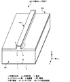
図1に、本開示の一実施形態に係る半導体レーザ素子の概略外観図を示す。なお、図1に示す例では、リッジ型(屈折率導波型)の半導体レーザ素子100を示すが、本開示はこれに限定されない。例えば、利得ガイド型の半導体レーザ素子に対しても、以下に説明する本開示の技術を適用することができる。
<1. Configuration of Semiconductor Laser Element>
[Overall configuration of semiconductor laser element]
FIG. 1 is a schematic external view of a semiconductor laser device according to an embodiment of the present disclosure. In the example shown in FIG. 1, a ridge type (refractive index guided type)
半導体レーザ素子100は、半導体基体1と、エピタキシャル層2と、絶縁層3と、第1電極4と、第2電極5とを備える。
The
本実施形態の半導体レーザ素子100では、半導体基体1の一方の面1a(図1では上面)は半極性面であり、該半極性面1a上に、エピタキシャル層2、絶縁層3及び第1電極4がこの順で形成される。また、半導体基体1の半極性面1aとは反対側の面1b(図1では下面:以下、裏面1bという)上には、第2電極5が形成される。なお、半導体基体1の半極性面1aとして、{2,0,−2,1}面付近の半極性面を用いた場合には、例えば、波長が500nm付近の緑色の光を発振させることができる。
In the
また、半導体レーザ素子100は、図1に示すように、略直方体状の形状を有し、半導体レーザ素子100の第1電極4側の表面には、所定方向(図1中のY方向)に延在したリッジ構造のストライプ部101が形成される。ストライプ部101は、半導体レーザ素子100の後述の一方の側面102から他方の側面103まで延在して形成される。そして、ストライプ部101の延在方向は、レーザ光の伝搬方向(導波方向)となり、ストライプ部101に対応するエピタキシャル層2の領域が光導波路となる。
As shown in FIG. 1, the
本実施形態では、レーザ光の伝搬方向を、レーザ光の伝搬方向を含みかつ半極性面1aと平行な光導波面の面内において、c軸を該光導波面に射影した軸の方向から約8度〜12度又は約18度〜29度の範囲の角度で傾けた方向に設定する。より具体的には、ストライプ部101の延在方向を、ストライプ部101の形成面において、c軸をストライプ部101の形成面に射影した軸の方向(以下、c軸の射影方向という)から約8度〜12度又は約18度〜29度の範囲の角度で傾けた方向に設定する。なお、ストライプ部101の延在方向を、ストライプ部101の形成面において、c軸の射影方向から上記角度範囲内の角度で傾ける理由は、後で詳述する。なお、ストライプ部101の幅は、数μm以下であり、ストライプ部101の延在長さ(共振器長)は、数百μm程度である。
In this embodiment, the propagation direction of the laser light is about 8 degrees from the direction of the axis projected on the optical waveguide surface in the plane of the optical waveguide surface including the propagation direction of the laser light and parallel to the
また、半導体レーザ素子100は、4つの側面(端面)を有し、該4つの側面のうち、ストライプ部101の延在方向(図1中のY方向)と略直交する2つの側面102,103(割断面)は、レーザ共振器の反射面として作用する。すなわち、2つの側面102,103はともに共振器端面であり、この2つの共振器端面102,103と、ストライプ部101に対応するエピタキシャル層2内の光導波路領域とにより、レーザ共振器が構成される。なお、後述のように、半導体レーザ素子100は、複数の半導体レーザ素子100が2次元状に配列して形成された基板部材(以下、生産基板という)から、切り出すことにより作製されるので、この4つの側面は、その切断処理時に形成された切断面である。
The
なお、本実施形態の半導体レーザ素子100では、2つの共振器端面102,103の少なくとも一方の表面上に、例えばSiO2/TiO2膜等の誘電体多層膜を形成(端面コート)してもよい。端面コートを行うことにより、共振器端面での反射率を調整することができる。
In the
[各部の構成]
ここで、本実施形態の半導体レーザ素子100の各部の構成を、より詳細に説明する。
[Configuration of each part]
Here, the configuration of each part of the
(1)半導体基体
半導体基体1は、例えば、GaN、AlN、AlGaN、InGaN、InAlGaN等の六方晶系III族窒化物半導体で形成される。また、半導体基体1としては、キャリアの導電型がn型の基板を用いることができる。そして、本実施形態では、上述のように、エピタキシャル層2、絶縁層3及び第1電極4が形成される半導体基体1の一方の面を半極性面1aで構成する。
(1) Semiconductor Base The
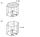
ここで、図2(a)及び(b)、並びに、図3に、GaNの結晶構造を示す。GaNは、図2(a)及び(b)に示すように、六方晶と呼ばれる結晶構造を有し、エピタキシャル層2内の後述する発光層に発生するピエゾ電界はc軸に沿って発生するので、c軸に直交するc面201({0,0,0,1}面)は、極性を有し、極性面と呼ばれる。一方、m軸に直交するm面202({1,0,−1,0}面)は、c軸に平行であるので無極性であり、無極性面と呼ばれる。それに対して、c軸をm軸方向に所定角度傾けた軸方向を法線方向とする面、例えば、図3に示す例では、c軸をm軸方向に75度傾けた軸方向を法線方向とする面({2,0,−2、1}面203)は、c面とm面との中間的な面となり、半極性面と呼ばれる。
Here, FIGS. 2A and 2B and FIG. 3 show the crystal structure of GaN. As shown in FIGS. 2A and 2B, GaN has a crystal structure called a hexagonal crystal, and a piezo electric field generated in a light emitting layer described later in the
なお、本実施形態では、半極性面1aとして、面方位が{2,0,−2、1}付近である面を用いる。具体的には、{2,0,−2、1}面、及び、この結晶面から微傾斜した(例えば±4度程度)結晶面を半極性面1aとして用いる。このような面方位の半極性面1aを用い、かつ、ストライプ部101の延在方向を、c軸の射影方向から約8度〜12度又は約18度〜29度の範囲の角度で傾けた場合、後述するように、直交性の優れた共振器端面102,103を形成することができる。
In the present embodiment, as the
また、半導体基体1の厚さは、例えば、約400μm以下に設定することができる。この厚さ範囲では、半導体レーザ素子の生産基板の割断処理時に、良質の(平坦性及び直交性の優れた)共振器端面102,103(割断面)を得ることができる。特に、半導体基体1の厚さを、例えば、約50μm〜100μmの範囲の値にした場合には、さらに良質の共振器端面102,103を形成することができる。
Moreover, the thickness of the
(2)エピタキシャル層、絶縁層、第1電極及び第2電極
次に、本実施形態の半導体レーザ素子100のエピタキシャル層2、絶縁層3、第1電極4及び第2電極5の構成を、図4を参照しながら説明する。図4は、半導体レーザ素子100の厚さ方向(図中のZ方向)の概略断面図である。なお、図4には、ストライプ部101の延在方向(図中のY方向)に直交する断面を示す。
(2) Epitaxial Layer, Insulating Layer, First Electrode and Second Electrode Next, the configuration of the
本実施形態では、エピタキシャル層2は、バッファ層11と、第1クラッド層12と、第1光ガイド層13と、発光層14(活性層)と、第2光ガイド層15と、キャリアブロック層16と、第2クラッド層17と、コンタクト層18とを備える。そして、バッファ層11、第1クラッド層12、第1光ガイド層13、発光層14、第2光ガイド層15、キャリアブロック層16、第2クラッド層17及びコンタクト層18は、半導体基体1の半極性面1a上に、この順で積層される。なお、ここでは、半導体基体1をn型のGaN半極性基板で構成した例を説明する。
In the present embodiment, the
バッファ層11は、例えばn型GaN層等の窒化ガリウム系半導体層で構成することができる。第1クラッド層12は、例えば、n型AlGaN層、n型InAlGaN等の窒化ガリウム系半導体層で構成することができる。また、第1光ガイド層13は、例えば、n型GaN層、n型InGaN層等の窒化ガリウム系半導体層で構成することができる。
The
発光層14は、例えば、InGaN、InAlGaN等の窒化ガリウム系半導体で形成された井戸層(不図示)と、例えば、GaN、InGaN、InAlGaN等の窒化ガリウム系半導体で形成された障壁層(不図示)とで構成される。そして、本実施形態では、発光層14の構造を、例えば、井戸層と障壁層とを交互に複数積層した多重量子井戸構造とすることができる。なお、発光層14は、エピタキシャル層2の発光領域となり、例えば、480nm〜550nm程度の範囲の波長の光を発光する。
The
第2光ガイド層15は、キャリアの導電型がp型の窒化ガリウム系半導体層で構成することができ、例えば、p型GaN層、p型InGaN層等の窒化ガリウム系半導体層で構成することができる。キャリアブロック層16(電子ブロック層)は、例えばp型AlGaN層で構成することができる。
The second
第2クラッド層17は、例えば、p型AlGaN層、p型InAlGaN層等の窒化ガリウム系半導体層で構成することができる。なお、本実施形態の半導体レーザ素子100は、リッジ型の半導体レーザ素子とするので、第2クラッド層17の第1電極4側の表面のストライプ部101に対応する領域以外の領域を、エッチング処理等により彫り込む。これにより、第2クラッド層17の第1電極4側の表面のストライプ部101に対応する領域に、リッジ部17aを形成する。なお、リッジ部17aは、ストライプ部101と同様に、各共振器端面と略直交する方向に延在して形成され、かつ、一方の共振器端面102から他方の共振器端面103まで延在して形成される。
The
コンタクト層18は、例えばp型GaN層で構成することができる。また、コンタクト層18は、第2クラッド層17のリッジ部17a上に形成される。
The
絶縁層3は、例えばSiO2膜等の絶縁膜で構成される。絶縁層3は、図4に示すように、第2クラッド層17のリッジ部17a以外の領域上、並びに、リッジ部17a及びコンタクト層18の側面上に形成される。
The insulating
第1電極4(p側電極)は、例えばPd膜等の導電膜で構成することができる。また、第1電極4は、コンタクト層18上、及び、絶縁層3のコンタクト層18側の端面上に形成される。なお、本実施形態の半導体レーザ素子100では、パッド電極用の電極膜を、絶縁層3及び第1電極4を覆うようにして設けてもよい。
The first electrode 4 (p-side electrode) can be composed of a conductive film such as a Pd film. The
第2電極5(n側電極)は、例えばAl膜等の導電膜で構成することができる。また、第2電極5は、半導体基体1の裏面1b上に形成される。
The second electrode 5 (n-side electrode) can be composed of a conductive film such as an Al film, for example. The
<2.半導体レーザ素子の製造方法>
次に、本実施形態の半導体レーザ素子100の製造手法を、図5を参照しながら具体的に説明する。なお、図5は、半導体レーザ素子100の製造手法の手順を示すフローチャートである。また、本実施形態では、半導体レーザ素子100の各共振器端面に誘電体多層膜を形成(端面コート)する例を説明する。
<2. Manufacturing method of semiconductor laser element>
Next, a method for manufacturing the
まず、複数の半導体レーザ素子100を2次元状に配置して形成するための六方晶系III族窒化物半導体で形成された半極性基板を用意する(ステップS10)。そして、用意した半極性基板に対してサーマルクリーニングを行う。
First, a semipolar substrate formed of a hexagonal group III nitride semiconductor for forming a plurality of
次いで、半極性基板の半極性面上に、例えばOMVPE(有機金属気相成長)法等の手法を用いて、各種半導体膜を所定の順序でエピタキシャル成長させて、エピタキシャル層2を構成する半導体膜群を形成する(ステップS20)。具体的には、半極性面上に、バッファ層11、第1クラッド層12、第1光ガイド層13、発光層14、第2光ガイド層15、キャリアブロック層16、第2クラッド層17及びコンタクト層18を構成する各半導体膜を、この順でエピタキシャル成長させる。
Next, a semiconductor film group constituting the
次いで、半極性基板の半導体膜群側の面上に、各半導体レーザ素子100のストライプ部101を形成する(ステップS30)。この際、半導体膜群側の面内において、各半導体レーザ素子100のストライプ部101の延在方向が、c軸の射影方向から約8度〜12度又は約18度〜29度の範囲の角度で傾いた方向になるように、各半導体レーザ素子100のストライプ部101を形成する。具体的は、次のようにしてストライプ部101を形成する。
Next, the
まず、半極性基板のコンタクト層18を構成する半導体膜側の表面領域のうち、ストライプ部101の形成領域にマスクを形成する。この際、マスクの延在方向が、マスクの形成面内において、c軸の射影方向から約8度〜12度又は約18度〜29度の範囲の角度で傾いた方向になるように、マスクを形成する。そして、マスクの形成領域以外の領域をエッチングし、各半導体レーザ素子100のコンタクト層18側の表面に、リッジを形成する(ステップS31)。
First, a mask is formed in the formation region of the
なお、この際、ストライプ部101の形成領域以外の領域を、コンタクト層18の表面から第2クラッド層17の所定深さまで彫り込み、ストライプ部101の形成領域にリッジを形成する。この処理により、各半導体レーザ素子100のコンタクト層18側の表面の面内において、c軸の射影方向から約8度〜12度又は約18度〜29度の範囲の所定角度で傾いた方向に延在したリッジが形成される。また、この際、ストライプ部101の延在方向に隣り合う2つの半導体レーザ素子100の形成領域間の境界をリッジが横切るように、リッジを連続して形成する。
At this time, a region other than the formation region of the
次いで、リッジ上のマスクを除去した後、半極性基板のリッジ側の表面に、例えば、蒸着法、スパッタ法等の手法を用いて、絶縁層3を構成する絶縁膜を形成する(ステップS32)。なお、リッジ上のマスクの除去は、絶縁膜の形成後でもよい。また、マスクを例えば金属などで形成した場合には、そのマスクを第1電極4の一部として使用することができるのでマスクを除去しなくてもよい。
Next, after removing the mask on the ridge, an insulating film constituting the insulating
次いで、上述のようにして半極性基板に各種半導体膜及び絶縁膜が形成された基板部材に、第1電極4及び第2電極5をそれぞれ構成する電極膜を形成する(ステップS33)。
Next, electrode films that respectively constitute the
具体的には、第1電極4を構成する電極膜(第1電極膜)は、次のようにして形成される。まず、フォトリソグラフィ技術を用いて、各リッジ上の絶縁膜を除去し、表面にコンタクト層18を露出させる。次いで、露出した各コンタクト層18上に、例えば、蒸着法、スパッタ法等の手法を用いて、第1電極4を構成する電極膜を形成する。
Specifically, the electrode film (first electrode film) constituting the
一方、第2電極5を構成する電極膜(第2電極膜)は、次のようにして形成される。まず、半極性基板の裏面を研磨して、半極性基板の厚さを所望の厚さに設定する。次いで、例えば、蒸着法、スパッタ法等の手法を用いて、半極性基板の裏面全体に渡って第2電極5を構成する電極膜を形成する。
On the other hand, the electrode film (second electrode film) constituting the
本実施形態では、上記ステップS31〜S33により、各半導体レーザ素子100のコンタクト層18側の表面の面内において、c軸の射影方向から約8度〜12度又は約18度〜29度の範囲の角度で傾いた方向に延在したストライプ部101を形成する。また、本実施形態では、上述したステップS10〜S30(S31〜S33)により、複数の半導体レーザ素子100を2次元状に配置して形成された生産基板を作製する。
In the present embodiment, in steps S31 to S33, a range of about 8 degrees to 12 degrees or about 18 degrees to 29 degrees from the c-axis projection direction in the surface on the
次に、ステップS40以降の処理、すなわち、生産基板から、各半導体レーザ素子100を切り出す処理(割断処理)の手順を説明する。なお、各半導体レーザ素子100を切り出す処理は、従来の手法と同様の手法を用いることができ、以下では、レーザスクライブ装置(不図示)を用いる手法について説明する。
Next, the procedure of the process after step S40, that is, the process of cutting out each
まず、各半導体レーザ素子100の共振器端面を形成する(ステップS40)。具体的には、生産基板をレーザスクライブ装置に装着し、生産基板に2次元状に配列された複数の半導体レーザ素子100の共振器端面に沿うスクライブラインの一部に、レーザビームを照射してスクライブ溝を形成する(ステップS41)。この際、例えば、生産基板のエッジ領域のスクライブライン上に、該スクライブラインに沿って、スクライブ溝を形成する。
First, the cavity end face of each
次いで、生産基板の裏面におけるスクライブ溝の形成領域と対向する領域に、ブレードと呼ばれるブレイキング装置(不図示)を押圧して、生産基板をスクライブラインに沿って割断(劈開)する(ステップS42)。そして、この割断処理を、各半導体レーザ素子100の共振器端面に沿うスクライブライン毎に繰り返し、生産基板を、複数の基板部材に分割する。なお、本実施形態では、割断(劈開)処理により、共振器端面を形成する例を説明したが、本開示はこれに限定されず、例えばドライエッチング処理等により、共振器端面を形成してもよい。
Next, a breaking device (not shown) called a blade is pressed against a region facing the formation region of the scribe groove on the back surface of the production substrate to cleave (cleave) the production substrate along the scribe line (step S42). Then, this cleaving process is repeated for each scribe line along the resonator end face of each
なお、本実施形態では、上述のように、各半導体レーザ素子100のストライプ部101の延在方向は、c軸の射影方向から約8度〜12度又は約18度〜29度の範囲内の所定角度で傾いた方向である。この場合、後で詳述するように、上記ステップS40で形成される共振器端面に露出し得る結晶面とストライプ部101の形成面(半極性面1a)と間の角度を理想値(90度)により近づけることができる。具体的には、例えば、共振器端面に露出し得る結晶面及びストライプ部101の形成面(半極性面1a)間の角度と、理想値(90度)との角度差を、例えば3度以下にすることができ、両者の直交性をより一層向上させることができる。
In the present embodiment, as described above, the extending direction of the
次いで、上記ステップS40で分離された各基板部材の割断面(共振器端面)に、誘電体多層膜を形成する(ステップS50)。そして、最後に、各基板部材の半導体レーザ素子100の共振器端面に沿うスクライブラインとは直交するスクライブラインの延在方向に沿って各基板部材を切断して、各基板部材を複数の半導体レーザ素子100のチップに分離する(ステップS60)。本実施形態では、上述のようにして半導体レーザ素子100を作製する。
Next, a dielectric multilayer film is formed on the section (resonator end face) of each substrate member separated in step S40 (step S50). Finally, each substrate member is cut along the extending direction of the scribe line perpendicular to the scribe line along the resonator end surface of the
<3.ストライプ部の構成>
次に、本実施形態の半導体レーザ素子100におけるストライプ部101の構成をより詳細に説明する。本実施形態の半導体レーザ素子100では、上述のように、ストライプ部101の延在方向を、その形成面内において、c軸の射影方向から約8度〜12度又は約18度〜29度の範囲の角度で傾いた方向に設定する。これにより、レーザ光の伝搬方向(ストライプ部101の延在方向)と共振器端面との直交性を向上させることができ、良好なレーザ特性を得ることができる。以下に、その理由を説明する。
<3. Stripe configuration>
Next, the configuration of the
(1)共振器端面の傾斜角の好適範囲
従来、半導体レーザ素子では、共振器端面を、レーザ光の導波路(ストライプ部)と直交するように形成する。さらに、その共振器端面に例えば誘電体等の材料からなる多層膜(誘電体多層膜)を形成して、例えば発振閾値電流Ith等の各種レーザ特性を改善する。具体的には、共振器端面に誘電体多層膜を形成することにより、共振器端面の反射率を、誘電体多層膜を共振器端面に形成していない場合(無コート状態時)のそれより向上させ、これにより、例えば発振閾値電流Ith等の各種レーザ特性を改善する。
(1) Preferred range of tilt angle of resonator end face Conventionally, in a semiconductor laser element, the end face of the resonator is formed so as to be orthogonal to the waveguide (stripe portion) of the laser beam. Furthermore, a multilayer film (dielectric multilayer film) made of a material such as a dielectric is formed on the end face of the resonator to improve various laser characteristics such as an oscillation threshold current Ith. Specifically, by forming a dielectric multilayer film on the resonator end face, the reflectivity of the resonator end face is higher than that when the dielectric multilayer film is not formed on the resonator end face (in the uncoated state). Thus, various laser characteristics such as the oscillation threshold current Ith are improved.
この際、レーザ特性を改善するために、通常、特にレーザ光を取り出さない共振器端面となるリア端面の反射率を、無コート状態時のそれより高くすることが一般的である。なお、レーザ光を取り出す共振器端面となるフロント端面においても、例えば、レーザ共振器長、用いる半導体の結晶性等の各種条件に依存するが、レーザ特性や設計の自由度などの観点から、フロント端面の反射率を高くしてもよい。すなわち、半導体レーザ素子では、実用上、無コート状態時の共振器端面の反射率より高い反射率を有する共振器端面を形成して、無コート状態時より多くの光をレーザ共振器内部に帰還させるようにしてもよい。 At this time, in order to improve the laser characteristics, it is general that the reflectance of the rear end face as a cavity end face from which laser light is not extracted is generally higher than that in the uncoated state. It should be noted that the front end face serving as the cavity end face from which the laser light is extracted also depends on various conditions such as the laser cavity length and the crystallinity of the semiconductor used, but from the viewpoint of laser characteristics and design freedom, The reflectance of the end face may be increased. That is, in a semiconductor laser device, a resonator end face having a higher reflectance than that of the resonator end face in an uncoated state is formed practically, and more light is fed back into the laser resonator than in the uncoated state. You may make it make it.
ここで、共振器端面の上述した定性的な構成条件を、理論計算を用いて、より定量的に説明する。無コート状態時の共振器端面の反射率Rは、R=(n0−n1)2/(n0+n1)2で計算することができる。ここで、n0は、媒質(一般的には空気)の屈折率であり、n1は半導体の屈折率である。なお、上記式で表される反射率Rは、レーザ光がその共振器端面に対して垂直に入射する場合の反射率である。 Here, the above-described qualitative configuration conditions of the resonator end face will be described more quantitatively using theoretical calculation. The reflectance R of the resonator end face in the uncoated state can be calculated by R = (n 0 −n 1 ) 2 / (n 0 + n 1 ) 2 . Here, n 0 is the refractive index of the medium (generally air), and n 1 is the refractive index of the semiconductor. The reflectance R represented by the above formula is a reflectance when the laser light is incident perpendicularly to the cavity end face.
例えば、InAlGaN系窒化物半導体の屈折率は、想定する光の波長や半導体組成によって変化するが、約2〜3の範囲の値であるので、このような4元系半導体を用いた半導体レーザ素子では、無コート状態時の反射率Rは約10%〜25%となる。それゆえ、InAlGaN系窒化物半導体レーザ素子では、共振器端面に入射される光の少なくとも10%の光をレーザ共振器内部に帰還させるようにする必要がある。また、InAlGaN系窒化物半導体レーザ素子では、好ましくは、共振器端面に入射される光の25%の光、さらに好ましくは、25%より十分大きな割合(量)の光をレーザ共振器内部に帰還させることが望ましい。 For example, the refractive index of an InAlGaN-based nitride semiconductor varies depending on the assumed wavelength of light and the semiconductor composition, but is a value in the range of about 2-3, so that a semiconductor laser device using such a quaternary semiconductor Then, the reflectance R in an uncoated state is about 10% to 25%. Therefore, in the InAlGaN-based nitride semiconductor laser element, it is necessary to feed back at least 10% of the light incident on the end face of the resonator into the laser resonator. In the InAlGaN-based nitride semiconductor laser element, preferably, 25% of the light incident on the end face of the resonator is returned to the inside of the laser resonator, more preferably a sufficiently large proportion (amount) of light. It is desirable to make it.
しかしながら、共振器端面とストライプ部の延在方向(レーザ光の伝搬方向)との間の直交性がくずれると、共振器端面による光の反射方向がレーザ光の伝搬方向と一致しなくなるため、共振端面における上記条件(光の帰還率条件)を満たすことが難しくなる。 However, if the orthogonality between the cavity end face and the extending direction of the stripe part (laser light propagation direction) is broken, the light reflection direction from the cavity end face does not coincide with the laser light propagation direction. It becomes difficult to satisfy the above condition (light feedback rate condition) at the end face.
そこで、本開示技術の提案者らは、理論計算により、共振器端面とストライプ部の延在方向(レーザ光の伝搬方向)との間の直交性のずれと、レーザ共振器内部に帰還される光の割合との関係を検証したところ、次のような知見が得られた。なお、この検証では、例えば、半導体の屈折率n1が2.5であり、縦方向(半導体基体の厚さ方向)の放射角が20度である一般的な窒化物半導体レーザ素子を考えた。また、この検証は、半導体レーザ素子より放出される光強度分布、及び、半導体レーザ素子内の光強度分布がともにガウス分布であり、且つ、光強度分布の広がりが屈折率比に反比例するという仮定に基づいて行った。さらに、この検証では、共振器端面とストライプ部の形成面との間の角度が90度(理想値)である場合の共振器端面の反射率を100%とした。 Therefore, the proponents of the disclosed technology are fed back to the inside of the laser resonator by the theoretical calculation and the deviation of the orthogonality between the end face of the resonator and the extending direction of the stripe portion (the propagation direction of the laser beam). When the relationship with the ratio of light was verified, the following findings were obtained. In this verification, for example, a general nitride semiconductor laser element in which the refractive index n 1 of the semiconductor is 2.5 and the emission angle in the vertical direction (thickness direction of the semiconductor substrate) is 20 degrees is considered. . This verification assumes that the light intensity distribution emitted from the semiconductor laser element and the light intensity distribution in the semiconductor laser element are both Gaussian and that the spread of the light intensity distribution is inversely proportional to the refractive index ratio. Based on. Further, in this verification, the reflectivity of the resonator end face when the angle between the end face of the resonator and the formation surface of the stripe portion is 90 degrees (ideal value) is 100%.
その結果、共振器端面とストライプ部の形成面との間の角度が90度から約3度傾くと、共振器内部に帰還される光の割合は25%に低下することが分かった。また、共振器端面とストライプ部の形成面との間の角度が90度から約6度傾くと、レーザ共振器内部に帰還される光の割合は10%に低下することが分かった。 As a result, it was found that when the angle between the resonator end face and the stripe forming surface is tilted from 90 degrees to about 3 degrees, the proportion of light returned to the inside of the resonator is reduced to 25%. Further, it was found that when the angle between the cavity end face and the stripe forming surface is tilted from 90 degrees to about 6 degrees, the ratio of light returned to the inside of the laser cavity is reduced to 10%.
以上の検証結果から、共振器端面とストライプ部の形成面との間の角度の理想値からのずれ量(傾斜角)を、6度以内、より好ましくは、3度以内とすることにより、共振器端面の上述した定性的な構成条件が満たされることが分かった。すなわち、理想的には共振器端面とストライプ部の形成面との間の角度は90度にすることが好ましいが、該角度が理想値からずれても、そのずれ量が6度以内、より好ましくは、3度以内であれば、十分良好なレーザ特性が得られることが分かった。なお、以下では、共振器端面とストライプ部の形成面との間の角度が90度(理想値)となるときの共振器端面を「理想端面」という。 From the above verification results, the resonance (reclination angle) of the angle between the resonator end face and the stripe forming surface from the ideal value is within 6 degrees, and more preferably within 3 degrees. It has been found that the above-described qualitative configuration conditions of the vessel end face are satisfied. That is, ideally, the angle between the resonator end face and the formation surface of the stripe portion is preferably 90 degrees, but even if the angle deviates from the ideal value, the deviation amount is preferably within 6 degrees. It was found that sufficiently good laser characteristics can be obtained within 3 degrees. Hereinafter, the resonator end face when the angle between the resonator end face and the stripe forming surface is 90 degrees (ideal value) is referred to as an “ideal end face”.
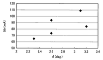
実際に、{2,0,−2,1}面を有する半極性基板を用いて作製したInAlGaN系窒化物半導体レーザ素子において、共振器端面の理想端面からの傾斜角(ずれ量)と、発振閾値電流Ithとの関係を調べた。なお、ここで作製したInAlGaN系窒化物半導体レーザ素子では、フロント端面及びリア端面のそれぞれに誘電体多層膜を設け、フロント端面の反射率を55%に調整し、リア端面の反射率を95%に調整した。 In fact, in an InAlGaN-based nitride semiconductor laser device fabricated using a semipolar substrate having a {2, 0, -2, 1} plane, the tilt angle (deviation amount) of the resonator end face from the ideal end face, and oscillation The relationship with the threshold current Ith was examined. In the InAlGaN-based nitride semiconductor laser device fabricated here, a dielectric multilayer film is provided on each of the front end face and the rear end face, the reflectance of the front end face is adjusted to 55%, and the reflectance of the rear end face is 95%. Adjusted.
図6に、その測定結果を示す。なお、図6に示す特性の横軸は、ストライプ部の形成面に対する共振器端面の角度の理想値(90度)からの傾斜角(ずれ量)、すなわち、共振器端面の理想端面からの傾斜角であり、縦軸は、発振閾値電流Ithである。図6に示すように、共振器端面の傾斜角が増加すると発振閾値電流Ithは増加するが、傾斜角が3度に近づくと、発振閾値電流Ithが大きくなり、さらに傾斜角が3度を越えると発振閾値電流Ithもさらに大きくなった。この測定結果からも、上述した理論計算による検証結果と同様に、好適なレーザ特性を得るためには、共振器端面の理想端面からの傾斜角を3度以下にすることがより望ましいことが分かる。 FIG. 6 shows the measurement results. Note that the horizontal axis of the characteristics shown in FIG. 6 represents the inclination angle (deviation amount) from the ideal value (90 degrees) of the angle of the resonator end face with respect to the formation surface of the stripe portion, that is, the inclination of the resonator end face from the ideal end face. The vertical axis represents the oscillation threshold current Ith. As shown in FIG. 6, the oscillation threshold current Ith increases as the inclination angle of the resonator end face increases. However, when the inclination angle approaches 3 degrees, the oscillation threshold current Ith increases and the inclination angle exceeds 3 degrees. The oscillation threshold current Ith is further increased. From this measurement result, it can be seen that, similarly to the verification result by the theoretical calculation described above, in order to obtain suitable laser characteristics, it is more desirable to set the inclination angle of the resonator end face from the ideal end face to 3 degrees or less. .
(2)ストライプ部の好適な延在方向
次に、面方位が{2,0,−2,1}である半極性面を有する半導体基体(以下、半極性基体という)を用いた六方晶系III族窒化物半導体レーザ素子におけるストライプ部の好ましい延在方向について説明する。
(2) Suitable extending direction of stripe portion Next, a hexagonal system using a semiconductor substrate having a semipolar plane whose plane orientation is {2, 0, -2, 1} (hereinafter referred to as a semipolar substrate). A preferred extending direction of the stripe portion in the group III nitride semiconductor laser device will be described.
一般に、半極性基体を用いた六方晶系III族窒化物半導体レーザ素子では、ストライプ部の延在方向(レーザ光の伝搬方向)は、c軸をストライプ部の形成面(半極性面)に射影した軸の方向(c軸の射影方向)に設定される。しかしながら、この場合、共振器端面は、例えばc面、m面、a面等(図2(a)及び(b)参照)のような劈開し易い面にならない。それゆえ、この場合には、ストライプ部の形成面と共振器端面との間の角度を90度(理想値)にすることが難く、共振器端面の理想端面からのずれ量(傾斜角)を、上記角度条件(6度以内、好ましくは、3度以内)を満たすように設定することが難しい。 In general, in a hexagonal group III-nitride semiconductor laser device using a semipolar substrate, the extending direction of the stripe portion (the propagation direction of the laser beam) projects the c-axis onto the formation surface (semipolar surface) of the stripe portion. The direction of the selected axis (c-axis projection direction) is set. However, in this case, the resonator end surface is not a surface that is easy to cleave, such as c-plane, m-plane, a-plane (see FIGS. 2A and 2B). Therefore, in this case, it is difficult to set the angle between the formation surface of the stripe portion and the resonator end surface to 90 degrees (ideal value), and the deviation amount (tilt angle) of the resonator end surface from the ideal end surface is reduced. It is difficult to set the angle condition (within 6 degrees, preferably within 3 degrees).
そこで、面方位が{2,0,−2,1}である半極性基体を用いた半導体レーザ素子において、ストライプ部の形成面と共振器端面との間の角度の理想値からのずれ量が上記角度条件を満たすようなストライプ部の延在方向が存在するか否かを数値解析により調べた。 Therefore, in a semiconductor laser device using a semipolar substrate whose plane orientation is {2, 0, -2, 1}, the deviation amount from the ideal value of the angle between the formation surface of the stripe portion and the resonator end face is small. It was examined by numerical analysis whether or not there is an extending direction of the stripe portion that satisfies the angle condition.
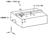
図7に、この数値解析で用いる半導体レーザ素子100の解析モデルの概略斜視図を示す。なお、数値解析の手法としては、ベクトル演算を用いた。
FIG. 7 shows a schematic perspective view of an analysis model of the
具体的には、六方晶系結晶の所定の結晶面({h,k,l,m}面)と、半極性面1a({2,0,−2,1}面)との間の角度αを、下記式(1)で算出した。
Specifically, the angle between a predetermined crystal plane ({h, k, l, m} plane) of the hexagonal crystal and the

また、所定の結晶面({h,k,l,m}面)を共振器端面102とした場合のストライプ部101の延在方向のc軸の射影方向からのずれ量dθ(傾斜角)を、下記式(2)で算出した。
Further, when the predetermined crystal plane ({h, k, l, m} plane) is the
なお、上記式(1)中のベクトル「Pe」は、各種結晶面({h,k,l,m}面:共振器端面)の面方位を示すベクトルであり、ベクトル「Ps」は、半極性面1aの面方位を示すベクトルである。また、上記式(2)中のベクトル「Pc」は、ストライプ部101の延在方向の基準となるc軸の射影方向を示すベクトルである。ただし、上記各種ベクトルは、六方晶系結晶の面指数(h、k、l及びm)を直交座標に変換したときのベクトルであり、上記各種ベクトルは、下記式(3)で表される。
The vector “Pe” in the above formula (1) is a vector indicating the plane orientation of various crystal planes ({h, k, l, m} plane: resonator end face), and the vector “Ps” is a half It is a vector which shows the surface orientation of the
また、上記式(3)中の「c」は、六方晶系結晶のc軸方向の格子定数であり、「a」は、六方晶系結晶のa軸方向の格子定数である。また、上記式(2)中のベクトル「Pes」は、ベクトル「Pe」の半極性面1aの面内方向成分であり、下記式(4)で表される。
In the above formula (3), “c” is a lattice constant in the c-axis direction of the hexagonal crystal, and “a” is a lattice constant in the a-axis direction of the hexagonal crystal. Further, the vector “Pes” in the above formula (2) is an in-plane direction component of the
なお、上記式(1)、(2)及び(4)中の「|V|」(Vは、ベクトルPe、Ps、Pes又はStr)はベクトルVの絶対値を示す。そして、数値解析では、六方晶系結晶の面指数h、k、l及びmをそれぞれ0〜±9の範囲で変化させて、上記式(1)〜(4)のベクトル演算を実施した。 In the above formulas (1), (2), and (4), “| V |” (V is the vector Pe, Ps, Pes, or Str) indicates the absolute value of the vector V. In the numerical analysis, the vector calculations of the above formulas (1) to (4) were performed by changing the plane indices h, k, l and m of the hexagonal crystal in the range of 0 to ± 9.
上記数値解析の結果を図8及び9に示す。なお、図8は、結晶面の理想端面からのずれ量δ(=90−α)が3度以下となる各種結晶面の面指数と、該各種結晶面に対応するストライプ部101の延在方向のc軸の射影方向からのずれ量dθ(傾斜角)との関係を示す表である。また、図9は、結晶面の理想端面からのずれ量δが3度より大きくかつ6度より小さくなる各種結晶面の面指数と、ストライプ部101の延在方向のc軸の射影方向からのずれ量dθとの関係を示す表である。
The results of the numerical analysis are shown in FIGS. FIG. 8 shows the plane index of various crystal planes where the deviation amount δ (= 90−α) of the crystal plane from the ideal end face is 3 degrees or less, and the extending direction of the
図8及び9に示すように、半極性基体を用いた六方晶系III族窒化物半導体レーザ素子では、半極性面1a({2,0,−2,1}面)と共振器端面との間の角度の理想値(90度)からのずれ量δが6度未満となる結晶面が多数存在することが分かった。しかしながら、半極性基体を用いた六方晶系III族窒化物半導体レーザ素子におけるレーザ光の偏光特性から、ストライプ部101の延在方向(レーザ光の伝搬方向)のずれ量dθ(傾斜角)が大きくなると、レーザ特性が劣化する。実際、上記特許文献1においても、半極性基体を用いた場合、ストライプ部101の延在方向がc軸に沿った方向であるときに光学利得が最大となり、ストライプ部101の延在方向がc軸に沿った方向からずれるほど光学利得が劣化することが指摘されている。それゆえ、ストライプ部101の延在方向(レーザ光の伝搬方向)のc軸の傾斜方向からのずれ量dθ(傾斜角)は、できる限り小さい方が好ましい。そして、良好な光学利得を得るという観点では、ずれ量dθの現実的な範囲は、約30度以下である。なお、ずれ量dθの上限は例えば必要とする特性等を考慮して適宜変更することができる。
As shown in FIGS. 8 and 9, in the hexagonal group III nitride semiconductor laser device using the semipolar substrate, the
そこで、共振器端面の理想端面からのずれ量δが3度以下となり、かつ、ストライプ部101の延在方向のc軸の傾斜方向からのずれ量dθが30度以下となる結晶面を図8から抽出すると、下記表1の結果が得られる。
Therefore, the crystal plane in which the deviation δ from the ideal end face of the resonator end face is 3 degrees or less and the deviation dθ from the c axis inclination direction in the extending direction of the
表1から、ストライプ部101の形成面と共振器端面との間の角度αの理想値からのずれ量δを3度以下にするためには、ストライプ部101の延在方向をc軸の射影方向から、10度、20度、22度、24度又は27度に傾ければよいことが分かった。特に、ストライプ部101の延在方向をc軸の射影方向から22度、24度又は27度とすることにより、共振器端面の理想端面からのずれ量δを2.3度以下にすることができ、共振器端面をより一層、理想端面に近づけることができる。すなわち、ストライプ部101の延在方向をc軸の射影方向から、22度、24度又は27度に傾けた場合には、ストライプ部101の延在方向と共振器端面との直交性をより一層向上させることができ、優れたレーザ特性が得られることが分かった。
From Table 1, in order to set the deviation δ from the ideal value of the angle α between the formation surface of the
なお、この場合、理想的には、ストライプ部101の延在方向のc軸の射影方向からの傾斜角を、高精度に22度、24度又は27度に設定することが望ましい。しかしながら、実際にストライプ部101を作製した場合には、製造誤差等により、ストライプ部101の延在方向のc軸の射影方向からの傾斜角(dθ)に、バラツキ(製造バラツキ)が生じる。それゆえ、翻って言うと、ストライプ部101の延在方向が製造バラツキ程度の範囲で所定方向からずれていても、そのずれは製造誤差に吸収されるので、実用上問題はない。そこで、ストライプ部101の延在方向の製造バラツキについて鋭意検討を行ったところ、±0.5度程度の製造バラツキが生じることが分かった。すなわち、ストライプ部101の延在方向のc軸の射影方向からの傾斜角(dθ)は、22度、24度又は27度から±0.5度程度ずれていてもよいことが分かった。
In this case, ideally, it is desirable to set the inclination angle from the projection direction of the c-axis in the extending direction of the
上記数値解析では、ストライプ部101の形成面と共振器端面との間の角度αの理想値(90度)からのずれ量δ、すなわち、半導体基体1の厚さ方向におけるストライプ部101の形成面と共振器端面との間の角度αのずれ量を解析した。しかしながら、ストライプ部101の延在方向と共振器端面との直交性を検証する際には、ストライプ部101の形成面内における、ストライプ部101の延在方向と共振器端面との間の角度のずれ量(水平ずれ量)も考慮する必要がある。
In the above numerical analysis, the deviation δ from the ideal value (90 degrees) of the angle α between the formation surface of the
ここで、図10に、ストライプ部101の形成面内における、ストライプ部101の延在方向と共振器端面との間の角度の水平ずれ量と、発振閾値電流Ithとの間の関係(実験結果)を示す。図10に示す特性の横軸は、ストライプ部101の形成面内における、共振器端面に対するストライプ部101の延在方向の理想値(90度)からの水平ずれ量(傾斜角:絶対値)であり、縦軸は、発振閾値電流Ithである。
Here, FIG. 10 shows the relationship between the horizontal deviation amount of the angle between the extending direction of the
図10に示すように、ストライプ部101の形成面内において、共振器端面に対するストライプ部101の延在方向の理想値(90度)からの水平ずれ量が、±2度以内であれば、発振閾値電流Ithの分布は大幅に悪化せず、良好な値が得られることが分かる。
As shown in FIG. 10, if the horizontal deviation from the ideal value (90 degrees) in the extending direction of the
上述した数値解析の結果(表1)及び実験結果(図10)から、ストライプ部101の延在方向を、c軸の射影方向から約8度〜12度又は約18度〜29度の範囲の角度で傾けることにより、優れたレーザ特性が得られることが分かった。
From the numerical analysis results (Table 1) and the experimental results (FIG. 10) described above, the extending direction of the
なお、本開示は、以下のような構成を取ることもできる。
(1)
六方晶系III族窒化物半導体で形成され、かつ、面方位が{2,0,−2,1}である半極性面を有する半導体基体と、
レーザ光の光導波路を形成する発光層を有し、前記半導体基体の前記半極性面上に形成され、かつ、該レーザ光の伝搬方向を含みかつ前記半極性面と平行な光導波面の面内において、該レーザ光の伝搬方向がc軸を該光導波面に射影した軸の方向から8度〜12度又は18度〜29度の範囲の角度で傾いた方向である、エピタキシャル層と、
前記レーザ光の前記光導波路の両端にそれぞれ設けられた2つの共振器端面と、
前記エピタキシャル層上に形成された第1電極と、
前記半導体基体の前記エピタキシャル層が形成される半極性面とは反対側の面上に形成された第2電極と
を備える半導体レーザ素子。
(2)
前記レーザ光の伝搬方向が、c軸を前記光導波面に射影した軸の方向から20度〜29度の範囲の角度で傾いた方向である
(1)に記載の半導体レーザ素子。
(3)
前記レーザ光の伝搬方向が、c軸を前記光導波面に射影した軸の方向から22度、24度及び27度のいずれかの角度で傾いた方向である
(2)に記載の半導体レーザ素子。
(4)
前記共振器端面と前記半極性面との間の角度の90度からずれ量が、3度以下の角度である
(1)〜(3)のいずれか一項に記載の半導体レーザ素子。
(5)
前記エピタキシャル層は、その前記第1電極側の表面に、前記レーザ光の伝搬方向に沿って延在したリッジ部を有する
(1)〜(4)のいずれか一項に記載の半導体レーザ素子。
(6)
六方晶系III族窒化物半導体で形成されかつ面方位が{2,0,−2,1}である半極性面を有する半導体基体の該半極性面上に、レーザ光の光導波路を形成する発光層を有し、かつ、該レーザ光の伝搬方向を含みかつ前記半極性面と平行な光導波面の面内において、該レーザ光の伝搬方向がc軸を該光導波面に射影した軸の方向から8度〜12度又は18度〜29度の範囲の角度で傾いた方向である、エピタキシャル層を形成するステップと、
前記エピタキシャル層上、及び、前記半導体基体の前記半極性面とは反対側の面上に、それぞれ、第1電極及び第2電極を形成するステップと、
前記レーザ光の前記光導波路の両端にそれぞれ2つの共振器端面を設けるステップと
を含む半導体レーザ素子の製造方法。
In addition, this indication can also take the following structures.
(1)
A semiconductor substrate formed of a hexagonal group III-nitride semiconductor and having a semipolar plane whose plane orientation is {2, 0, -2, 1};
A light-emitting layer that forms an optical waveguide of laser light, and is formed on the semipolar surface of the semiconductor substrate, and includes a propagation direction of the laser light and is parallel to the semipolar surface. In the epitaxial layer, the propagation direction of the laser light is inclined at an angle in the range of 8 degrees to 12 degrees or 18 degrees to 29 degrees from the direction of the axis projected from the c-axis to the optical waveguide surface;
Two resonator end faces respectively provided at both ends of the optical waveguide of the laser light;
A first electrode formed on the epitaxial layer;
A semiconductor laser device comprising: a second electrode formed on a surface opposite to a semipolar surface on which the epitaxial layer of the semiconductor substrate is formed.
(2)
The semiconductor laser device according to (1), wherein a propagation direction of the laser light is a direction inclined at an angle in a range of 20 degrees to 29 degrees from an axis direction obtained by projecting a c-axis onto the optical waveguide surface.
(3)
The semiconductor laser device according to (2), wherein the propagation direction of the laser light is a direction inclined at any angle of 22 degrees, 24 degrees, and 27 degrees from the direction of the axis projected from the c-axis onto the optical waveguide surface.
(4)
The semiconductor laser device according to any one of (1) to (3), wherein an amount of deviation from an angle of 90 degrees between the resonator end face and the semipolar plane is an angle of 3 degrees or less.
(5)
The said epitaxial layer has a ridge part extended along the propagation direction of the said laser beam in the surface at the side of the said 1st electrode, The semiconductor laser element as described in any one of (1)-(4).
(6)
An optical waveguide for laser light is formed on the semipolar plane of a semiconductor substrate formed of a hexagonal group III nitride semiconductor and having a semipolar plane with a plane orientation of {2, 0, -2, 1}. In the plane of the optical waveguide surface having a light emitting layer and including the propagation direction of the laser light and parallel to the semipolar surface, the propagation direction of the laser light is the direction of the axis projected from the c-axis onto the optical waveguide surface Forming an epitaxial layer in a direction inclined at an angle in the range of 8 degrees to 12 degrees or 18 degrees to 29 degrees,
Forming a first electrode and a second electrode on the epitaxial layer and on a surface opposite to the semipolar surface of the semiconductor substrate, respectively;
Providing two resonator end faces at both ends of the optical waveguide of the laser light, respectively.
1…半導体基体、1a…半極性面、1b…裏面、2…エピタキシャル層、3…絶縁層、4…第1電極、5…第2電極、11…バッファ層、12…第1クラッド層、13…第1光ガイド層、14…発光層、15…第2光ガイド層、16…キャリアブロック層、17…第2クラッド層、18…コンタクト層、100…半導体レーザ素子、101…ストライプ部、102,103…共振器端面
DESCRIPTION OF
Claims (6)
レーザ光の光導波路を形成する発光層を有し、前記半導体基体の前記半極性面上に形成され、かつ、該レーザ光の伝搬方向を含みかつ前記半極性面と平行な光導波面の面内において、該レーザ光の伝搬方向がc軸を該光導波面に射影した軸の方向から8度〜12度又は18度〜29度の範囲の角度で傾いた方向である、エピタキシャル層と、
前記レーザ光の前記光導波路の両端にそれぞれ設けられた2つの共振器端面と、
前記エピタキシャル層上に形成された第1電極と、
前記半導体基体の前記エピタキシャル層が形成される半極性面とは反対側の面上に形成された第2電極と
を備える半導体レーザ素子。 A semiconductor substrate formed of a hexagonal group III-nitride semiconductor and having a semipolar plane whose plane orientation is {2, 0, -2, 1};
A light-emitting layer that forms an optical waveguide of laser light, and is formed on the semipolar surface of the semiconductor substrate, and includes a propagation direction of the laser light and is parallel to the semipolar surface. In the epitaxial layer, the propagation direction of the laser light is inclined at an angle in the range of 8 degrees to 12 degrees or 18 degrees to 29 degrees from the direction of the axis projected from the c-axis to the optical waveguide surface;
Two resonator end faces respectively provided at both ends of the optical waveguide of the laser light;
A first electrode formed on the epitaxial layer;
A semiconductor laser device comprising: a second electrode formed on a surface opposite to a semipolar surface on which the epitaxial layer of the semiconductor substrate is formed.
請求項1に記載の半導体レーザ素子。 2. The semiconductor laser device according to claim 1, wherein a propagation direction of the laser light is a direction inclined at an angle in a range of 22 degrees to 27 degrees from an axis direction in which a c-axis is projected onto the optical waveguide surface.
請求項2に記載の半導体レーザ素子。 The semiconductor laser device according to claim 2, wherein a propagation direction of the laser light is a direction inclined at any angle of 22 degrees, 24 degrees, and 27 degrees from the direction of an axis obtained by projecting the c-axis onto the optical waveguide surface.
請求項1に記載の半導体レーザ素子。 The semiconductor laser device according to claim 1, wherein a deviation amount from 90 degrees of an angle between the resonator end face and the semipolar plane is an angle of 3 degrees or less.
請求項1に記載の半導体レーザ素子。 2. The semiconductor laser device according to claim 1, wherein the epitaxial layer has a ridge portion extending along a propagation direction of the laser light on a surface of the first electrode side.
前記エピタキシャル層上、及び、前記半導体基体の前記半極性面とは反対側の面上に、それぞれ、第1電極及び第2電極を形成するステップと、
前記レーザ光の前記光導波路の両端にそれぞれ2つの共振器端面を設けるステップと
を含む半導体レーザ素子の製造方法。
An optical waveguide for laser light is formed on the semipolar plane of a semiconductor substrate formed of a hexagonal group III nitride semiconductor and having a semipolar plane with a plane orientation of {2, 0, -2, 1}. In the plane of the optical waveguide surface having a light emitting layer and including the propagation direction of the laser light and parallel to the semipolar surface, the propagation direction of the laser light is the direction of the axis projected from the c-axis onto the optical waveguide surface Forming an epitaxial layer in a direction inclined at an angle in the range of 8 degrees to 12 degrees or 18 degrees to 29 degrees,
Forming a first electrode and a second electrode on the epitaxial layer and on a surface opposite to the semipolar surface of the semiconductor substrate, respectively;
Providing two resonator end faces at both ends of the optical waveguide of the laser light, respectively.
Priority Applications (3)
| Application Number | Priority Date | Filing Date | Title |
|---|---|---|---|
| JP2012005367A JP2013145799A (en) | 2012-01-13 | 2012-01-13 | Laser diode and method of manufacturing laser diode |
| CN2013100038771A CN103208740A (en) | 2012-01-13 | 2013-01-06 | Laser Diode And Method Of Manufacturing Laser Diode |
| US13/735,746 US20130182734A1 (en) | 2012-01-13 | 2013-01-07 | Laser diode and method of manufacturing laser diode |
Applications Claiming Priority (1)
| Application Number | Priority Date | Filing Date | Title |
|---|---|---|---|
| JP2012005367A JP2013145799A (en) | 2012-01-13 | 2012-01-13 | Laser diode and method of manufacturing laser diode |
Publications (2)
| Publication Number | Publication Date |
|---|---|
| JP2013145799A true JP2013145799A (en) | 2013-07-25 |
| JP2013145799A5 JP2013145799A5 (en) | 2014-10-02 |
Family
ID=48755875
Family Applications (1)
| Application Number | Title | Priority Date | Filing Date |
|---|---|---|---|
| JP2012005367A Pending JP2013145799A (en) | 2012-01-13 | 2012-01-13 | Laser diode and method of manufacturing laser diode |
Country Status (3)
| Country | Link |
|---|---|
| US (1) | US20130182734A1 (en) |
| JP (1) | JP2013145799A (en) |
| CN (1) | CN103208740A (en) |
Families Citing this family (2)
| Publication number | Priority date | Publication date | Assignee | Title |
|---|---|---|---|---|
| DE102016113071A1 (en) | 2016-07-15 | 2018-01-18 | Osram Opto Semiconductors Gmbh | Semiconductor laser diode |
| CN108376731A (en) * | 2018-02-07 | 2018-08-07 | 赛富乐斯股份有限公司 | Light-emitting device and its manufacturing method |
Citations (4)
| Publication number | Priority date | Publication date | Assignee | Title |
|---|---|---|---|---|
| JP2003264340A (en) * | 2002-03-11 | 2003-09-19 | Nichia Chem Ind Ltd | Gallium nitride based compound semiconductor multistripe laser and optical fiber system |
| JP2011003660A (en) * | 2009-06-17 | 2011-01-06 | Sumitomo Electric Ind Ltd | Group iii nitride semiconductor laser element, and method of manufacturing group iii nitride semiconductor laser element |
| JP2011068503A (en) * | 2009-09-24 | 2011-04-07 | Sumitomo Electric Ind Ltd | Nitride semiconductor substrate |
| JP2011138891A (en) * | 2009-12-28 | 2011-07-14 | Nichia Corp | Nitride semiconductor element |
Family Cites Families (4)
| Publication number | Priority date | Publication date | Assignee | Title |
|---|---|---|---|---|
| JP2010518626A (en) * | 2007-02-12 | 2010-05-27 | ザ リージェンツ オブ ザ ユニバーシティ オブ カリフォルニア | Optimization of laser rod orientation for nonpolar and semipolar (Ga, Al, In, B) N diode lasers |
| US8284810B1 (en) * | 2008-08-04 | 2012-10-09 | Soraa, Inc. | Solid state laser device using a selected crystal orientation in non-polar or semi-polar GaN containing materials and methods |
| US7933303B2 (en) * | 2009-06-17 | 2011-04-26 | Sumitomo Electric Industries, Ltd. | Group-III nitride semiconductor laser device, and method for fabricating group-III nitride semiconductor laser device |
| KR101833379B1 (en) * | 2009-11-05 | 2018-02-28 | 더 리전츠 오브 더 유니버시티 오브 캘리포니아 | Semipolar {20-21} III-nitride laser diodes with etched mirrors |
-
2012
- 2012-01-13 JP JP2012005367A patent/JP2013145799A/en active Pending
-
2013
- 2013-01-06 CN CN2013100038771A patent/CN103208740A/en active Pending
- 2013-01-07 US US13/735,746 patent/US20130182734A1/en not_active Abandoned
Patent Citations (4)
| Publication number | Priority date | Publication date | Assignee | Title |
|---|---|---|---|---|
| JP2003264340A (en) * | 2002-03-11 | 2003-09-19 | Nichia Chem Ind Ltd | Gallium nitride based compound semiconductor multistripe laser and optical fiber system |
| JP2011003660A (en) * | 2009-06-17 | 2011-01-06 | Sumitomo Electric Ind Ltd | Group iii nitride semiconductor laser element, and method of manufacturing group iii nitride semiconductor laser element |
| JP2011068503A (en) * | 2009-09-24 | 2011-04-07 | Sumitomo Electric Ind Ltd | Nitride semiconductor substrate |
| JP2011138891A (en) * | 2009-12-28 | 2011-07-14 | Nichia Corp | Nitride semiconductor element |
Also Published As
| Publication number | Publication date |
|---|---|
| CN103208740A (en) | 2013-07-17 |
| US20130182734A1 (en) | 2013-07-18 |
Similar Documents
| Publication | Publication Date | Title |
|---|---|---|
| US8389312B2 (en) | Group-III nitride semiconductor laser device, and method of fabricating group-III nitride semiconductor laser device | |
| JP5425172B2 (en) | Semiconductor laser device and manufacturing method of semiconductor laser device | |
| US8772064B2 (en) | Group-III nitride semiconductor laser device, and method of fabricating group-III nitride semiconductor laser device | |
| US8213475B2 (en) | Group-III nitride semiconductor laser device, and method for fabricating group-III nitride semiconductor laser device | |
| JP5234130B2 (en) | Optical semiconductor device | |
| JP2003017791A (en) | Nitride semiconductor device and its manufacturing method | |
| JP5471256B2 (en) | Semiconductor device, semiconductor wafer, semiconductor wafer manufacturing method, semiconductor device manufacturing method | |
| JP5451724B2 (en) | Manufacturing method of semiconductor laser device | |
| JP2011077326A (en) | Semiconductor laser integrated element and method for manufacturing the same | |
| JP2010186791A (en) | Semiconductor light-emitting element, and method for manufacturing the same | |
| JP4966591B2 (en) | Manufacturing method of semiconductor light emitting device | |
| JP5664627B2 (en) | Group III nitride semiconductor laser device, method of manufacturing group III nitride semiconductor laser device, method of evaluating end face for optical resonator of group III nitride semiconductor laser device, method of evaluating scribe groove | |
| JP2012124273A (en) | Semiconductor laser element | |
| JP2011124521A (en) | Semiconductor laser and method of manufacturing the same | |
| JP2013145799A (en) | Laser diode and method of manufacturing laser diode | |
| JP4959644B2 (en) | Semiconductor laser device, semiconductor wafer, and manufacturing method of semiconductor laser device | |
| JP4984514B2 (en) | Semiconductor light emitting device and method for manufacturing the semiconductor light emitting device | |
| JP5624166B2 (en) | Nitride semiconductor wafer | |
| JP2015159193A (en) | Semiconductor light-emitting element, method of manufacturing the same, and wafer for semiconductor light-emitting element | |
| JP2006339311A (en) | Semiconductor laser | |
| WO2021100604A1 (en) | Semiconductor laser and manufacturing method for semiconductor laser | |
| JP2000114666A (en) | Semiconductor light emitting element and manufacturing method | |
| JP5245031B2 (en) | Method for forming nitride-based semiconductor layer | |
| JP2008181928A (en) | Semiconductor laser and manufacturing method thereof | |
| JP2015005614A (en) | Method for producing group iii nitride semiconductor laser element |
Legal Events
| Date | Code | Title | Description |
|---|---|---|---|
| A521 | Request for written amendment filed |
Free format text: JAPANESE INTERMEDIATE CODE: A523 Effective date: 20140820 |
|
| A621 | Written request for application examination |
Free format text: JAPANESE INTERMEDIATE CODE: A621 Effective date: 20140820 |
|
| A977 | Report on retrieval |
Free format text: JAPANESE INTERMEDIATE CODE: A971007 Effective date: 20150422 |
|
| A131 | Notification of reasons for refusal |
Free format text: JAPANESE INTERMEDIATE CODE: A131 Effective date: 20150512 |
|
| A521 | Request for written amendment filed |
Free format text: JAPANESE INTERMEDIATE CODE: A523 Effective date: 20150713 |
|
| A131 | Notification of reasons for refusal |
Free format text: JAPANESE INTERMEDIATE CODE: A131 Effective date: 20151006 |
|
| A521 | Request for written amendment filed |
Free format text: JAPANESE INTERMEDIATE CODE: A523 Effective date: 20151201 |
|
| A02 | Decision of refusal |
Free format text: JAPANESE INTERMEDIATE CODE: A02 Effective date: 20160301 |