JP4984514B2 - Semiconductor light emitting device and method for manufacturing the semiconductor light emitting device - Google Patents
Semiconductor light emitting device and method for manufacturing the semiconductor light emitting device Download PDFInfo
- Publication number
- JP4984514B2 JP4984514B2 JP2005360122A JP2005360122A JP4984514B2 JP 4984514 B2 JP4984514 B2 JP 4984514B2 JP 2005360122 A JP2005360122 A JP 2005360122A JP 2005360122 A JP2005360122 A JP 2005360122A JP 4984514 B2 JP4984514 B2 JP 4984514B2
- Authority
- JP
- Japan
- Prior art keywords
- layer
- semiconductor light
- emitting device
- light emitting
- active layer
- Prior art date
- Legal status (The legal status is an assumption and is not a legal conclusion. Google has not performed a legal analysis and makes no representation as to the accuracy of the status listed.)
- Active
Links
Images


Description
本発明は、光ファイバ通信や計測・診断用光源に適する高出力スーパールミネッセントダイオード(以下、「SLD」と称する)を含む半導体発光素子およびその製造方法に関するものである。 The present invention relates to a semiconductor light-emitting device including a high-power superluminescent diode (hereinafter referred to as “SLD”) suitable for optical fiber communication and a light source for measurement / diagnosis, and a method for manufacturing the same.
近年、ファイバジャイロや高分解能OTDRなど光計測の分野で必要とされるインコヒーレント光源としてSLDが注目されている。SLDは半導体レーザ同様に注入キャリアの再結合により生じた自然放出光が、光出射端面方向に進む間に誘導放出による高い利得を受けて増幅され、光出射端面から放出される素子である。SLDは端面反射による共振器の形成を抑え、FP(ファブリ・ペロー)モード発振が生じないようにしている点が半導体レーザとは異なる。SLDは通常の発光ダイオード同様にインコヒーレント性を示し広い帯域なスペクトル形状を示すと共に、数十mW程度までの出力を得ることが可能である。 In recent years, SLDs have attracted attention as incoherent light sources required in the field of optical measurement such as fiber gyros and high-resolution OTDR. The SLD is an element in which spontaneous emission light generated by recombination of injected carriers is amplified by receiving a high gain due to stimulated emission while traveling in the direction of the light emission end face, and emitted from the light emission end face, as in the semiconductor laser. SLDs differ from semiconductor lasers in that they prevent the formation of resonators due to end-face reflection and prevent FP (Fabry-Perot) mode oscillation. The SLD is incoherent like a normal light emitting diode, exhibits a broad spectrum shape, and can output up to several tens of mW.
このようなSLDにおいて、より広帯域な(広い波長範囲に亘る)スペクトル分布を得る方法として(1)光の導波方向の構造を用いる方法(例えば、特許文献1参照。)および(2)活性層の厚み方向の構造を用いる方法(例えば、非特許文献1参照。)が知られている。 In such an SLD, (1) a method using a structure in the waveguide direction of light (see, for example, Patent Document 1) and (2) an active layer as a method for obtaining a broader spectrum distribution (over a wide wavelength range). A method using a structure in the thickness direction is known (for example, see Non-Patent Document 1).
(2)の方法は、互いに異なるバンドギャップをもつ複数の層を活性層に用い、それぞれのバンドギャップにおいて発光する光スペクトルが重ね合わさり、出射される光スペクトルを広帯域化する方法である。しかし、この構造において、活性層の層数や層厚みなどを増すと、駆動電流密度が増加するため、複数の活性層を必要とする広帯域化素子に大きな負荷がおよび素子の寿命を向上することが難しかった。 The method (2) is a method in which a plurality of layers having mutually different band gaps are used as active layers, the light spectra emitted in the respective band gaps are superimposed, and the emitted light spectrum is broadened. However, in this structure, when the number of active layers and the thickness of the active layer are increased, the drive current density increases, so that a large load is applied to a broadband device that requires a plurality of active layers and the life of the device is improved. It was difficult.
一方、(1)の方法は、幅の異なるマスクを作製した後に活性層を成膜することで、活性層の導波方向に厚み分布と組成分布を持たせ、導波方向にバンドギャップを連続的、あるいは不連続的に変化させることで、広帯域化する方法であり、広帯域化によって駆動電流増加などの負荷が発生することはない。これは、活性層の厚みや組成が異なることにより利得波長が異なることを利用するものである。 On the other hand, in the method (1), after forming masks having different widths, an active layer is formed so that the active layer has a thickness distribution and a composition distribution in the waveguide direction, and a band gap is continuously formed in the waveguide direction. This is a method of widening the band by changing the power or discontinuously, and no load such as an increase in driving current is generated by the widening of the band. This utilizes the fact that the gain wavelength varies depending on the thickness and composition of the active layer.
従来、(1)のように導波方向に厚み分布および組成分布を持たせる方法としては、活性層成膜前にSiO2やSiNなどの絶縁膜で選択成長マスクを作製し、その選択成長マスクを用いて活性層を選択成長させる方法が用いられる。具体的には、積層面上に2つのストライプ状のSiO2マスクを互いに一定間隔を開けて平行に形成し、且つマスク幅を変えることでマスクに挟まれた領域に成長した活性層の膜厚・組成を共振器軸方向に変化させる方法が知られている。
上記(1)の方法を用いて作製した、導波方向に異なる利得波長の光を生じる構造を備えたSLDは通常の単一の利得波長の光のみを生じる構造のSLDと比較して広い帯域のスペクトル分布を得ることができる。 The SLD manufactured using the method (1) and having a structure that generates light having a different gain wavelength in the waveguide direction has a wider bandwidth than an SLD that generates only light having a single gain wavelength. Can be obtained.
一方、この方法はマスク部分表面の原料が活性層やその他のマスク外へマイグレーションすることを利用したものであるため、さらなる広帯域化を行うためには、マスク幅の変化量を大きくする必要がある。マスク幅の変化量を大きくするためには、全体としてのマスク面積を大きくする必要があるが、一般的にMOCVDの選択成長において、マスク面積が大きくなると、選択成長後のエッチング工程などによって除去することができない多結晶がマスク面上に析出しやすくなるという問題があり、マスク面積が制限される。従って、素子の広帯域化にも限界があった。 On the other hand, since this method utilizes the fact that the raw material on the mask portion surface migrates outside the active layer and other masks, it is necessary to increase the amount of change in the mask width in order to further increase the bandwidth. . In order to increase the amount of change in the mask width, it is necessary to increase the mask area as a whole. In general, however, in the selective growth of MOCVD, if the mask area increases, it is removed by an etching process after the selective growth. There is a problem that polycrystals that cannot be easily deposited on the mask surface, and the mask area is limited. Therefore, there is a limit to the expansion of the device bandwidth.
本発明は上記事情に鑑みて、SLDなどの半導体発光素子において、利得波長の広帯域化を図ることができる新規な構造の半導体発光素子およびその製造方法を提供することを目的とするものである。 SUMMARY OF THE INVENTION In view of the above circumstances, an object of the present invention is to provide a semiconductor light emitting device having a novel structure capable of increasing the gain wavelength in a semiconductor light emitting device such as an SLD and a method for manufacturing the same.
本発明の半導体発光素子は、基板上に、下部クラッド層、活性層および上部クラッド層を含む複数の半導体層が積層されてなり、利得導波型および/または屈折率導波型の光導波路を有する半導体発光素子において、
前記複数の半導体層のうち、前記活性層よりも基板側の半導体層の積層面に凹部が形成されており、
該積層面より上に前記活性層および該活性層より上の層が積層されており、
前記光導波路が、前記凹部の少なくとも一部と平面視上で重なるように配置されていることを特徴とするものである。
The semiconductor light-emitting device of the present invention is formed by laminating a plurality of semiconductor layers including a lower clad layer, an active layer, and an upper clad layer on a substrate. In a semiconductor light emitting device having
Of the plurality of semiconductor layers, a recess is formed on the laminated surface of the semiconductor layer on the substrate side of the active layer,
The active layer and the layer above the active layer are laminated above the lamination surface,
The optical waveguide is arranged so as to overlap with at least a part of the recess in plan view.
凹部の形状はいかなる形状であってもよいが、前記積層面には凹部が形成されることにより基板と平行な面と異なる面方位の面が露出され、その異なる面方位の面が露出して複数の異なる面方位の面を有する積層面上に、該積層面を有する半導体層より上層の半導体層が積層されているものとする。なお、凹部はエッチングにより形成されたものであることが望ましい。 The shape of the concave portion may be any shape, but by forming the concave portion on the laminated surface, a surface having a different plane orientation from the plane parallel to the substrate is exposed, and the plane having the different plane orientation is exposed. It is assumed that a semiconductor layer above the semiconductor layer having the stacked surface is stacked on a stacked surface having a plurality of surfaces having different plane orientations. Note that the recess is preferably formed by etching.
凹部がストライプ状である場合、光導波路が凹部と前記平面視上で交差する方向に延びるように配置されていてもよいし、光導波路と凹部とが同一方向に延びるように配置されていてもよい。 When the concave portion is in a stripe shape, the optical waveguide may be arranged to extend in a direction intersecting the concave portion in the plan view, or the optical waveguide and the concave portion may be arranged to extend in the same direction. Good.
本発明の半導体発光素子は、スーパールミネッセントダイオードとして用いてもよいし、光増幅器として用いてもよい。 The semiconductor light emitting device of the present invention may be used as a superluminescent diode or an optical amplifier.
本発明の半導体発光素子の製造方法は、基板上に、下部クラッド層、活性層および上部クラッド層を含む複数の半導体層が積層されてなり、利得導波型および/または屈折率導波型の光導波路を有する半導体発光素子の製造方法であって、
前記基板上に、前記複数の半導体層のうち前記活性層より下層の半導体層を積層し、
該半導体層の積層面に凹部を形成し、
該凹部が形成された前記積層面より上に、前記活性層および該活性層より上の層を積層すると共に、前記凹部の少なくとも一部と平面視上で重なりを有するように前記光導波路を形成することを特徴とする。
In the method for manufacturing a semiconductor light emitting device of the present invention, a plurality of semiconductor layers including a lower clad layer, an active layer, and an upper clad layer are laminated on a substrate. A method of manufacturing a semiconductor light emitting device having an optical waveguide,
Laminating a semiconductor layer below the active layer among the plurality of semiconductor layers on the substrate,
Forming a recess in the laminated surface of the semiconductor layer;
The active layer and the layer above the active layer are laminated above the laminated surface where the concave portion is formed, and the optical waveguide is formed so as to overlap with at least a part of the concave portion in plan view. It is characterized by doing.
なおここで、凹部は積層面に基板と平行な面とは異なる面方位の面を露出するために形成されるものであり、形状はいかなるものであってもよい。凹部の形成には例えば、エッチング法を用いることができる。また、選択成長法を用いて凹部を形成してもよい。 Here, the concave portion is formed to expose a surface having a plane orientation different from the surface parallel to the substrate on the laminated surface, and may have any shape. For example, an etching method can be used to form the recess. Moreover, you may form a recessed part using the selective growth method.
本発明の半導体発光素子は、活性層よりも基板側の半導体層の積層面に凹部が形成されて、該凹部が形成されて積層面に異なる面方位が露出した上に活性層などの他の層が積層されているので、該積層面より上の層の厚みは凹部に沿った領域と、他の領域とで異なる厚みで成長したものとなっており、光導波路が凹部の少なくとも一部と平面視上で重なるように配置されているので、光導波路内の活性層の厚みも凹部と重なる部分と他の部分とで異なるものとなっている。従って、活性層の厚みの変化により、利得波長に幅が生じるために広帯域化された光出力を得ることができる。 In the semiconductor light emitting device of the present invention, a recess is formed on the stacking surface of the semiconductor layer on the substrate side of the active layer, and the recess is formed so that a different plane orientation is exposed on the stacking surface, and another active layer or the like is exposed. Since the layers are laminated, the thickness of the layer above the laminated surface is grown with a different thickness in the region along the recess and in other regions, and the optical waveguide is at least part of the recess. Since they are arranged so as to overlap in plan view, the thickness of the active layer in the optical waveguide is also different between the portion overlapping the recess and the other portion. Accordingly, since the gain wavelength has a width due to the change in the thickness of the active layer, a broadband optical output can be obtained.
本発明の半導体発光素子は広帯域な光出力を得ることができるので、スーパールミネッセントダイオードとして、OTDRなどの光計測の光源に好適に用いることができる。 Since the semiconductor light emitting device of the present invention can obtain a broadband optical output, it can be suitably used as a light source for optical measurement such as OTDR as a superluminescent diode.
本発明の半導体発光素子の製造方法によれば、積層面に凹部を形成することにより、積層面に異なる面方位となる面を露出させることができ、面方位が異なると、その上に成長される半導体層の成長レートが異なることから、該積層面より上に積層させる活性層はその凹部に沿った領域と、他の領域とで異なる厚みで成長されたものとなる。光導波路をこの凹部の一部と平面視上で重なりを有するように形成するので、その光導波路内の活性層の厚みを、凹部と重なる部分と他の部分とで異なるものとすることができる。活性層の厚みが変化すると利得波長が変化することから本製造方法で製造された半導体発光素子は活性層の厚み変化による利得波長の幅を有し、広帯域な光出力を得ることができるものとなる。 According to the method for manufacturing a semiconductor light emitting device of the present invention, by forming a recess in the laminated surface, it is possible to expose a surface having a different surface orientation on the laminated surface, and when the surface orientation is different, the surface is grown thereon. Since the growth rate of the semiconductor layer differs, the active layer to be laminated above the lamination surface is grown with different thicknesses in the region along the recess and in other regions. Since the optical waveguide is formed so as to overlap with a part of the recess in plan view, the thickness of the active layer in the optical waveguide can be different between the part overlapping the recess and the other part. . Since the gain wavelength changes when the thickness of the active layer changes, the semiconductor light emitting device manufactured by this manufacturing method has a gain wavelength width due to the change of the thickness of the active layer, and can obtain a broadband optical output. Become.
活性層の厚みに変化を持たせる方法として従来のような選択成長マスクを用いないのでマスク上に多結晶が析出するという問題も生じることなく、広帯域化を実現することができる。 As a method for changing the thickness of the active layer, since a conventional selective growth mask is not used, a wide band can be realized without causing a problem of polycrystals being deposited on the mask.
以下、本発明の実施の形態について説明する。 Embodiments of the present invention will be described below.
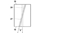
図1は、本発明の第1の実施形態の半導体発光素子の断面図であり、図2は図1に示した半導体発光素子中の凹部と光導波路との関係を模式的に表した平面図である。 FIG. 1 is a cross-sectional view of a semiconductor light emitting device according to a first embodiment of the present invention, and FIG. 2 is a plan view schematically showing a relationship between a recess and an optical waveguide in the semiconductor light emitting device shown in FIG. It is.
本実施形態の半導体発光素子は、基板1上に、下部クラッド層3、活性層5および上部クラッド層7、9を含む複数の半導体層が積層されてなり、メサストライプ型リッジ構造25による光導波路を有する半導体発光素子である。複数の半導体層のうち、活性層5よりも基板1側の下部クラッド層3の積層面に凹部20が形成されており、該積層面より上に活性層5および該活性層5より上の層が積層されており、光導波路27が、凹部20の少なくとも一部と平面視上で重なるように配置されている。なお、光導波路27はメサストライプ型リッジ構造25により規定されるものであり、メサストライプの平面視上における形状および配置は光導波路27とほぼ一致している。
In the semiconductor light emitting device of this embodiment, a plurality of semiconductor layers including a
なお、本素子は図2に示すように光導波路が端面18,19の法線方向に傾きを有するように配置されており、両端面18、19にAR膜コーティングを施されているので共振器構造は形成されずSLDとして発光する。
In this element, as shown in FIG. 2, the optical waveguide is arranged so as to be inclined in the normal direction of the end faces 18 and 19, and the AR films are applied to both
図3A〜3Eは図1および図2に示す半導体発光素子の製造工程を示す斜視図である。本実施形態の半導体発光素子は、赤外発光を示すSLDである。図3A〜3Eを参照して半導体発光素子の具体的な層構成および作製方法を説明する。 3A to 3E are perspective views showing manufacturing steps of the semiconductor light emitting device shown in FIGS. 1 and 2. The semiconductor light emitting device of this embodiment is an SLD that emits infrared light. With reference to FIGS. 3A to 3E, a specific layer structure and a manufacturing method of the semiconductor light emitting element will be described.
半導体層の積層は、有機金属気相成長(MOCVD)法を用いて結晶成長を行う。原料にはTEG(トリエチルガリウム)、TMA(トリメチルアルミニウム)、TMI(トリメチルインジウム)、AsH3(アルシン)、PH3(ホスフィン)、ドーパントとしてSiH4(シラン)、DEZ(ジエチル亜鉛)を用いる。 The semiconductor layer is stacked by crystal growth using a metal organic chemical vapor deposition (MOCVD) method. The raw material TEG (triethyl gallium), TMA (trimethyl aluminum), TMI (trimethyl indium), AsH 3 (arsine), PH 3 (phosphine), SiH 4 as a dopant (silane), using DEZ (diethylzinc).
n型GaAs基板1の(100)面上に、MOCVD法により成長温度600℃〜700℃、成長温度10.3kPaの条件下にてn型GaAsバッファ層(0.2μm厚、キャリア濃度5.0×1017cm-3)2、n型In0.49Ga0.51P下部クラッド層(2.0μm厚、キャリア濃度5.0×1017cm-3)3を成長する(図3A参照)。
An n-type GaAs buffer layer (0.2 μm thick, carrier concentration 5.0 × 10 17 cm) on the (100) surface of the n-
下部クラッド層3の積層面上に、リソグラフィープロセスにより、幅5μmのストライプ状開口部を端面の法線方向に作製し、図3Bに示すように下部クラッド層3をストライプ状に100nmエッチングしてストライプ状の凹部20を形成する。
A stripe-shaped opening having a width of 5 μm is formed on the laminated surface of the lower
レジストを除去した後に、MOCVD法によりノンドープGaAs下部光ガイド層(0.034nm厚)4、InGaAs多重量子井戸活性層(1.1μm発光)5、ノンドープGaAs上部光ガイド層(0.034nm厚)6、p型In0.49Ga0.51P上部第1クラッド層(0.2μm厚、キャリア濃度7.0×1017cm-3)7、p型 GaAsエッチングストップ層(100Å厚、キャリア濃度7.0×1017cm-3)8、p型In0.49Ga0.51P上部第2クラッド層(0.5μm厚、キャリア濃度7.0×1017cm-3)9およびp型GaAsキャップ層(0.2μm厚、キャリア濃度7.0×1017cm-3)10を順に積層配置する(図3C参照)。 After removing the resist, the non-doped GaAs lower light guide layer (0.034 nm thickness) 4, InGaAs multiple quantum well active layer (1.1 μm emission) 5, non-doped GaAs upper light guide layer (0.034 nm thickness) 6, p-type by MOCVD In 0.49 Ga 0.51 P upper first cladding layer (0.2 μm thick, carrier concentration 7.0 × 10 17 cm −3 ) 7, p-type GaAs etching stop layer (100 mm thick, carrier concentration 7.0 × 10 17 cm −3 ) 8, p Type In 0.49 Ga 0.51 P upper second cladding layer (0.5 μm thickness, carrier concentration 7.0 × 10 17 cm −3 ) 9 and p-type GaAs cap layer (0.2 μm thickness, carrier concentration 7.0 × 10 17 cm −3 ) 10 The layers are sequentially stacked (see FIG. 3C).
キャップ層10の上に誘電体マスクとなるSiO2選択成長マスクを形成(図示せず)してp-GaAsキャップ層10、p型In0.49Ga0.51P上部第2クラッド層9をエッチングして、メサストライプ状のリッジ構造25を形成する(図3D参照)。ここでメサストライプ状リッジ構造25により形成される光導波路は光出射端面18、19に対して傾きを有するようにし、かつ下部クラッド層3に作製したストライプ状の凹部20と7°の角度をなすようにして交差させる。
A SiO 2 selective growth mask serving as a dielectric mask is formed on the cap layer 10 (not shown), and the p-
その後SiO2マスクを用いた選択成長法により、p-GaAsエッチングストップ層8の上、メサストライプ状リッジ25を除く領域にn-In0.49(Al0.12Ga0.88)0.51P電流ブロック層(0.5μm厚、キャリア濃度1.0×1018cm-3)11を3回目の結晶成長により形成する。さらに、SiO2マスクを除去した後に、メサストライプ状リッジ25および電流ブロック層11の全面に対してp型Al0.58Ga0.42As上部第3クラッド層(1.3μm厚、キャリア濃度7.0×1017cm-3)12、p-GaAsコンタクト層(2.0μm厚、キャリア濃度1.0×1019cm-3)13を4回目の結晶成長により形成する(図3E参照)。
After that, n-In 0.49 (Al 0.12 Ga 0.88 ) 0.51 P current blocking layer (0.5 μm thick) is formed on the p-GaAs
その後全体の厚みが100μm程度になるまで基板の研磨を行い、最後にn側電極14を基板1裏面に、p側電極15をコンタクト層13上に蒸着および熱処理により形成する。このウエハから端面18、19間長さ0.50〜2.0mm程度のSLDバ−を劈開により切り出し、端面18、19に素子の発光波長に対して0.5%以下の反射率のAR膜コ−ティングを行う。その後劈開によりチップ化を行いSLD素子が形成される。チップは、放熱効果を高めるため発光部のあるpn接合部を下にしてヒートシンクに実装を行うことが望ましい。
Thereafter, the substrate is polished until the total thickness becomes about 100 μm, and finally the n-
一般に、薄膜を結晶成長させる場合、積層面の結晶の面方位によって異なる成長レートで成長することが知られている。従って、上記のような凹部上に結晶成長させる場合、凹部の基板に平行な(100)面(図3B中符号21で示す面)上とエッチングによって生じた傾斜面(図3B中符号22で示す面)上とでは成長レートが異なるため同一結晶成長時間で成長させた場合にそれぞれの面上に成長する膜の膜厚が異なる。例えば、活性層のInGaAsのIn組成の割合が5%のとき、成長温度750℃で、基板に平行な(100)面と斜面(011)の成長レートの比は8:5である。従って、活性層の膜厚を(100)面に成長される結晶で80Åに設定した場合、斜面では50Åになる。したがって、光導波路が凹部と交差するように形成されている場合、その光導波路中の活性層は厚みが50−80Åの間で変化した部分を含むこととなる。
In general, it is known that when a thin film is crystal-grown, it grows at different growth rates depending on the crystal plane orientation of the laminated surface. Therefore, when the crystal is grown on the concave portion as described above, the (100) plane parallel to the substrate of the concave portion (the surface indicated by
さて一方、図4は、InGaAsのIn組成の割合毎(0%、5%、10%、20%、30%、40%、50%)の活性層の厚みと利得波長(遷移波長)との関係を示すものである。図4に示すように、活性層の厚みが変化すると利得波長が変化する。上述のように、InGaAsのIn組成の割合が5%で活性層厚が50−80Åで変化している素子では、利得波長が約30nmの幅で変化するため、活性層厚が一定である素子と比較して広帯域なスペクトルが得られる。 On the other hand, FIG. 4 shows the active layer thickness and gain wavelength (transition wavelength) for each InGaAs In composition ratio (0%, 5%, 10%, 20%, 30%, 40%, 50%). It shows the relationship. As shown in FIG. 4, the gain wavelength changes as the thickness of the active layer changes. As described above, in the device in which the In composition ratio of InGaAs is 5% and the active layer thickness is changed from 50 to 80 mm, the gain wavelength is changed with a width of about 30 nm. Therefore, the active layer thickness is constant. Compared with, a broad spectrum is obtained.
なお、Inの組成を大きくしていった場合は、In組成の面方位依存性が存在し、異なる面方位の面に成長させることにより組成比も変化すると考えられ、さらなる広帯域化が期待できる。また、成長温度を変えると(100)面と斜面の成長レートの比が変化する場合もあるため、成長温度によって、帯域を広げることも可能である。 When the In composition is increased, the In composition has a plane orientation dependency, and it is considered that the composition ratio is changed by growing on a plane having a different plane orientation, and further broadening of the band can be expected. Further, since the ratio of the growth rate between the (100) plane and the slope may change when the growth temperature is changed, the band can be expanded depending on the growth temperature.
なお、それぞれの組成における成長温度と、各面方位における成長レートなどは材料によって異なるため、成長温度と各面方位毎の成長レート(あるいは成長レートの比)が未知である場合には、予めそれらを調べた上で組成、活性層厚と波長との関係と照らしわせ、所望の波長幅を得ることができる活性層厚幅を求めて成長時の温度、時間などを設定する必要がある。 In addition, since the growth temperature in each composition and the growth rate in each plane orientation differ depending on the material, if the growth temperature and the growth rate for each plane orientation (or the ratio of the growth rate) are unknown, they are preliminarily determined. In view of the above, it is necessary to set the temperature, time, etc. during growth by obtaining the active layer thickness width that can obtain a desired wavelength width in light of the relationship between the composition, the active layer thickness, and the wavelength.
上記実施形態において光ガイド層の材料組成および層厚、電流ブロック層の材料組成および層厚、クラッド層の材料組成および層厚は発光波長が単一モードで発光する条件の1例を示したものであり、本発明は前述の材料組成、層厚に限定されるものではない。またここでは屈折率導波型と利得導波型を組み合わせた埋込型リッジストライプ構造による光導波路を備えたSLD素子を挙げたが、屈折率導波型の内部ストライプ構造によるものなど他の構造による光導波路を備えた素子であってもよい。 In the above embodiment, the material composition and layer thickness of the light guide layer, the material composition and layer thickness of the current blocking layer, and the material composition and layer thickness of the cladding layer show an example of the conditions for emitting light in a single mode. Therefore, the present invention is not limited to the above-described material composition and layer thickness. In this example, the SLD element with an optical waveguide with a buried ridge stripe structure that combines a refractive index waveguide type and a gain waveguide type is mentioned. However, other structures such as those with a refractive index guided type internal stripe structure are mentioned. An element including an optical waveguide according to the above may be used.
また、上記実施形態においては、活性層より基板側の半導体層の積層面に設けられる凹部として1本のストライプ状凹部を形成するものとしたが、凹部は、基板に平行な面とは異なる面方位の面を露出させるために設けるものであり、その形状はストライプ形状である必要はなく任意の形状とすることができ、凹部の数は単数であっても複数であってもよい。また、ストライプ状凹部の場合も1本に限らず複数本あってもよい。さらには、テーパー状に幅が変化する凹部であってもよい。なお、光導波路に垂直な複数のストライプ状凹部を設ける場合、周期的なストライプ状凹部により共振器構造が形成されることを避けるため、ストライプ状凹部の形成周期が発光スペクトル波長の1/2波長の整数倍にならないように設定する必要があり、光導波路に垂直な周期的なストライプ状凹部は形成しないことが望ましい。 Moreover, in the said embodiment, although one stripe-shaped recessed part was formed as a recessed part provided in the lamination | stacking surface of the semiconductor layer of the substrate side from an active layer, a recessed part is a surface different from a surface parallel to a board | substrate. It is provided to expose the azimuth plane, and the shape does not need to be a stripe shape and can be an arbitrary shape, and the number of recesses may be singular or plural. Further, the number of stripe-shaped recesses is not limited to one, and a plurality of stripe-shaped recesses may be provided. Further, it may be a concave portion whose width changes in a tapered shape. When providing a plurality of stripe-shaped recesses perpendicular to the optical waveguide, the formation period of the stripe-shaped recesses is 1/2 wavelength of the emission spectrum wavelength in order to avoid the formation of the resonator structure due to the periodic stripe-shaped recesses. Therefore, it is desirable not to form periodic stripe-shaped concave portions perpendicular to the optical waveguide.
なお、導波路を形成するリッジと凹部の関係を任意に設定することで、任意のスペクトル形状を得ることができる。例えば、長波長側のスペクトル強度の大きなスペクトル形状を得たい場合、該長波長の光を発光する領域(例えば活性層厚み80Åの領域)と重なる面積が大きくなるように、凹部もしくはメサストライプリッジに曲率を持たせ、長波長領域の重なり部が短波長領域の重なり部に対して大きくなるような構造にすればよい。 Note that an arbitrary spectral shape can be obtained by arbitrarily setting the relationship between the ridge forming the waveguide and the recess. For example, when it is desired to obtain a spectral shape with a large spectral intensity on the long wavelength side, the concave portion or the mesa stripe ridge is formed so that the area overlapping the region emitting light of the long wavelength (for example, the region having an active layer thickness of 80 mm) is large. What is necessary is just to make it a structure which gives a curvature and the overlap part of a long wavelength region becomes large with respect to the overlap part of a short wavelength region.
また、上記実施形態においては、凹部を下部クラッド層の上面に形成するものとしたが、活性層よりも基板側の層であればどの層でもよい。例えば、バッファ層の上面あるいは、下部クラッド層を2層構造とし、基板側の下部クラッド層の上面に凹部を設けてもよい。 In the above embodiment, the concave portion is formed on the upper surface of the lower clad layer. However, any layer may be used as long as it is a layer closer to the substrate than the active layer. For example, the upper surface of the buffer layer or the lower cladding layer may have a two-layer structure, and a recess may be provided on the upper surface of the lower cladding layer on the substrate side.
以下、凹部と光導波路との配置が異なる他の例について説明する。層構成および製造方法は上述の実施形態と同様のものを採用することができる。図5から図7は第2から第4の実施形態の半導体発光素子の平面図であり、素子内部に形成されている凹部と光導波路がそれぞれ破線で示されている。 Hereinafter, another example in which the arrangement of the concave portion and the optical waveguide is different will be described. The layer configuration and manufacturing method can be the same as those in the above-described embodiment. FIGS. 5 to 7 are plan views of the semiconductor light emitting devices of the second to fourth embodiments, in which concave portions and optical waveguides formed in the device are indicated by broken lines.
図5に示す第2の実施形態の半導体発光素子は、素子の前方端面18から後方端面19に向けて幅が徐々に広がったテーパー状の凹部31を備え、光導波路32が後方側で凹部31と重なるように配置されているものである。
The semiconductor light emitting device of the second embodiment shown in FIG. 5 includes a tapered
図6に示す第3の実施形態の半導体発光素子は、素子の端面18、19に平行な方向に延びるストライプ状の凹部34と、端面の法線方向に延び、凹部34と直交するように配置された光導波路35とを備えている。
The semiconductor light emitting device of the third embodiment shown in FIG. 6 is arranged so that a
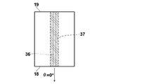
図7に示す第4の実施形態の半導体発光素子は、素子の端面18、19の法線方向に延びるストライプ状の凹部36と該凹部36の幅より広い幅を有し、該凹部36と平行に配置された光導波路37とを備えている。なお、図7の半導体発光素子のように、光導波路37が凹部36の全域と重なる場合には、凹部36の幅は光導波路37の幅と同程度以下であることが望ましい。
The semiconductor light emitting device of the fourth embodiment shown in FIG. 7 has a
いずれの実施形態の素子についても光導波路が凹部と平面視上で重なるように形成されて、光導波路内の活性層の層厚が部分的に変化していることから、利得波長に幅が生じ、広帯域なスペクトルの光出力を得ることができる。従って、光計測のための装置の光源として好適に用いることができる。 In any of the embodiments, the optical waveguide is formed so as to overlap with the recess in plan view, and the thickness of the active layer in the optical waveguide is partially changed. A broadband optical output can be obtained. Therefore, it can be suitably used as a light source of an apparatus for optical measurement.
なお、上記各実施形態の半導体発光素子はSLDとしてのみならず光増幅器として用いることもできる。 In addition, the semiconductor light emitting device of each of the above embodiments can be used not only as an SLD but also as an optical amplifier.
1 n型GaAs基板
2 n型GaAsバッファ層
3 n型In0.49Ga0.51P下部クラッド層
4 ノンドープGaAs下部光ガイド層
5 InGaAs多重量子井戸活性層
6 ノンドープGaAs上部光ガイド層
7 p型In0.49Ga0.51P上部第1クラッド層
8 p型 GaAsエッチングストップ層
9 p型In0.49Ga0.51P上部第2クラッド層
10 p型GaAsキャップ層
11 n-In0.49(Al0.12Ga0.88)0.51P電流ブロック層
12 p型Al0.58Ga0.42As上部第3クラッド層
13 p-GaAsコンタクト層
14 n側電極
15 p側電極
18、19 端面
20 凹部
25 メサストライプ状リッジ
1 n-type GaAs substrate 2 n-type GaAs buffer layer 3 n-type In 0.49 Ga 0.51 P lower cladding layer 4 non-doped GaAs lower
10 p-type GaAs cap layer
11 n-In 0.49 (Al 0.12 Ga 0.88 ) 0.51 P current blocking layer
12 p-type Al 0.58 Ga 0.42 As upper third cladding layer
13 p-GaAs contact layer
14 n-side electrode
15 p-side electrode
18, 19 End face
20 Recess
25 Mesa Striped Ridge
Claims (5)
前記複数の半導体層のうち、前記活性層よりも基板側の半導体層の積層面に前記基板の面に平行な面の面方位とは異なる面方位の斜面を有する凹部が形成されており、
該積層面より上に前記活性層および該活性層より上の層が積層されており、
前記光導波路が、前記凹部の少なくとも前記斜面を含む一部と平面視上で重なるように、かつ該平面視上で前記凹部と重なっていない部分を有するように配置されていることを特徴とする半導体発光素子。 In a semiconductor light emitting device having a gain waveguide type and / or a refractive index waveguide type optical waveguide, wherein a plurality of semiconductor layers including a lower cladding layer, an active layer, and an upper cladding layer are laminated on a substrate.
Of the plurality of semiconductor layers, a concave portion having a slope with a plane orientation different from the plane orientation of the plane parallel to the plane of the substrate is formed on the laminated surface of the semiconductor layer on the substrate side of the active layer,
The active layer and the layer above the active layer are laminated above the lamination surface,
The optical waveguide is disposed so as to overlap a part including at least the slope of the concave part in a plan view and to have a part not overlapping the concave part in the plan view. Semiconductor light emitting device.
前記光導波路が前記凹部と前記平面視上で交差する方向に延びるように配置されていることを特徴とする請求項1記載の半導体発光素子。 The recess is striped,
2. The semiconductor light emitting element according to claim 1, wherein the optical waveguide is disposed so as to extend in a direction intersecting with the concave portion in the plan view.
前記基板上に、前記複数の半導体層のうち前記活性層より下層の半導体層を積層し、
該半導体層の積層面に前記基板の面に平行な面の面方位とは異なる面方位の斜面を有する凹部を形成し、
該凹部が形成された前記積層面より上に、前記活性層および該活性層より上の層を積層すると共に、前記凹部の少なくとも前記斜面を含む一部と平面視上で重なりを有するように、かつ該平面視上で前記凹部と重なっていない部分を有するように前記光導波路を形成することを特徴とする半導体発光素子の製造方法。 A method of manufacturing a semiconductor light emitting device having a gain waveguide type and / or a refractive index waveguide type optical waveguide, wherein a plurality of semiconductor layers including a lower clad layer, an active layer, and an upper clad layer are laminated on a substrate. There,
Laminating a semiconductor layer below the active layer among the plurality of semiconductor layers on the substrate,
Forming a recess having a slope with a plane orientation different from the plane orientation of the plane parallel to the plane of the substrate on the lamination surface of the semiconductor layer;
The active layer and a layer above the active layer are stacked above the stacked surface on which the recess is formed, and so as to overlap with at least a part of the recess including the slope in a plan view. The method of manufacturing a semiconductor light-emitting element includes forming the optical waveguide so as to have a portion that does not overlap the concave portion in plan view.
Priority Applications (1)
| Application Number | Priority Date | Filing Date | Title |
|---|---|---|---|
| JP2005360122A JP4984514B2 (en) | 2005-12-14 | 2005-12-14 | Semiconductor light emitting device and method for manufacturing the semiconductor light emitting device |
Applications Claiming Priority (1)
| Application Number | Priority Date | Filing Date | Title |
|---|---|---|---|
| JP2005360122A JP4984514B2 (en) | 2005-12-14 | 2005-12-14 | Semiconductor light emitting device and method for manufacturing the semiconductor light emitting device |
Publications (2)
| Publication Number | Publication Date |
|---|---|
| JP2007165599A JP2007165599A (en) | 2007-06-28 |
| JP4984514B2 true JP4984514B2 (en) | 2012-07-25 |
Family
ID=38248162
Family Applications (1)
| Application Number | Title | Priority Date | Filing Date |
|---|---|---|---|
| JP2005360122A Active JP4984514B2 (en) | 2005-12-14 | 2005-12-14 | Semiconductor light emitting device and method for manufacturing the semiconductor light emitting device |
Country Status (1)
| Country | Link |
|---|---|
| JP (1) | JP4984514B2 (en) |
Families Citing this family (3)
| Publication number | Priority date | Publication date | Assignee | Title |
|---|---|---|---|---|
| CN102804416B (en) | 2010-03-23 | 2015-04-15 | 松下电器产业株式会社 | Semiconductor light emitting element and method for manufacturing same |
| JP2012033797A (en) * | 2010-08-02 | 2012-02-16 | Panasonic Corp | Semiconductor light-emitting element |
| CN111261756B (en) * | 2020-03-25 | 2021-12-14 | 武汉光谷信息光电子创新中心有限公司 | Semiconductor light emitting device |
Family Cites Families (3)
| Publication number | Priority date | Publication date | Assignee | Title |
|---|---|---|---|---|
| JPH02246181A (en) * | 1989-03-20 | 1990-10-01 | Canon Inc | Semiconductor photoamplifier |
| JP2770496B2 (en) * | 1989-11-21 | 1998-07-02 | 三菱電機株式会社 | Optical amplifier, super luminescent diode, optical integrated circuit, and manufacturing method thereof |
| JPH04373182A (en) * | 1991-06-21 | 1992-12-25 | Mitsubishi Electric Corp | Manufacture of semiconductor light emitting device |
-
2005
- 2005-12-14 JP JP2005360122A patent/JP4984514B2/en active Active
Also Published As
| Publication number | Publication date |
|---|---|
| JP2007165599A (en) | 2007-06-28 |
Similar Documents
| Publication | Publication Date | Title |
|---|---|---|
| US6184542B1 (en) | Superluminescent diode and optical amplifier with extended bandwidth | |
| JP5185537B2 (en) | Optical semiconductor device and manufacturing method thereof | |
| JP2007165689A (en) | Super luminescent diode | |
| JP2004241570A (en) | Semiconductor laser device | |
| JP2009065048A (en) | Semiconductor light-emitting element and method of manufacturing the same | |
| JP2015519008A (en) | Laser with improved beam shape | |
| WO2011121678A1 (en) | Semiconductor laser array and method for manufacturing semiconductor laser array | |
| JP2004253811A (en) | Semiconductor light emitting device and its manufacturing method | |
| US20060086941A1 (en) | Superluminescent diode including active layer formed of various sized quantum dots and method of manufacturing the same | |
| JP2002353559A (en) | Semiconductor laser and method of manufacturing the same | |
| JP5595483B2 (en) | Semiconductor light emitting device and manufacturing method thereof | |
| CN112542769B (en) | Wide-spectrum multi-wavelength Fabry-Perot laser and manufacturing method thereof | |
| JP4984514B2 (en) | Semiconductor light emitting device and method for manufacturing the semiconductor light emitting device | |
| US20040013144A1 (en) | Complex-coupled distributed feedback semiconductor laser device | |
| JP2007184526A (en) | Super luminescent diode and method of manufacturing same | |
| JP2011124521A (en) | Semiconductor laser and method of manufacturing the same | |
| US20050123018A1 (en) | Ridge type distributed feedback semiconductor laser | |
| US20020080835A1 (en) | Semiconductor laser and method of production thereof | |
| WO2018020793A1 (en) | Semiconductor light-emitting element and method for manufacturing semiconductor light-emitting element | |
| US20080198890A1 (en) | Vertically emitting laser and method of making the same | |
| JPH1056200A (en) | Light emitting diode and its manufacture | |
| JP3186645B2 (en) | Semiconductor laser and method of manufacturing the same | |
| JP2004087564A (en) | Semiconductor laser element and manufacturing method thereof | |
| WO2020181497A1 (en) | Double-cavity dfb laser chip, optical emission component, optical module, and optical network device | |
| JP2005268573A (en) | Semiconductor light emitting element using self-forming quantum dot |
Legal Events
| Date | Code | Title | Description |
|---|---|---|---|
| A621 | Written request for application examination |
Free format text: JAPANESE INTERMEDIATE CODE: A621 Effective date: 20080714 |
|
| A977 | Report on retrieval |
Free format text: JAPANESE INTERMEDIATE CODE: A971007 Effective date: 20101124 |
|
| A131 | Notification of reasons for refusal |
Free format text: JAPANESE INTERMEDIATE CODE: A131 Effective date: 20101214 |
|
| A521 | Request for written amendment filed |
Free format text: JAPANESE INTERMEDIATE CODE: A523 Effective date: 20110204 |
|
| A131 | Notification of reasons for refusal |
Free format text: JAPANESE INTERMEDIATE CODE: A131 Effective date: 20110308 |
|
| A521 | Request for written amendment filed |
Free format text: JAPANESE INTERMEDIATE CODE: A523 Effective date: 20110411 |
|
| A711 | Notification of change in applicant |
Free format text: JAPANESE INTERMEDIATE CODE: A711 Effective date: 20120214 |
|
| TRDD | Decision of grant or rejection written | ||
| A01 | Written decision to grant a patent or to grant a registration (utility model) |
Free format text: JAPANESE INTERMEDIATE CODE: A01 Effective date: 20120403 |
|
| A01 | Written decision to grant a patent or to grant a registration (utility model) |
Free format text: JAPANESE INTERMEDIATE CODE: A01 |
|
| A61 | First payment of annual fees (during grant procedure) |
Free format text: JAPANESE INTERMEDIATE CODE: A61 Effective date: 20120416 |
|
| R150 | Certificate of patent or registration of utility model |
Ref document number: 4984514 Country of ref document: JP Free format text: JAPANESE INTERMEDIATE CODE: R150 Free format text: JAPANESE INTERMEDIATE CODE: R150 |
|
| FPAY | Renewal fee payment (event date is renewal date of database) |
Free format text: PAYMENT UNTIL: 20150511 Year of fee payment: 3 |
|
| FPAY | Renewal fee payment (event date is renewal date of database) |
Free format text: PAYMENT UNTIL: 20150511 Year of fee payment: 3 |
|
| R250 | Receipt of annual fees |
Free format text: JAPANESE INTERMEDIATE CODE: R250 |
|
| R250 | Receipt of annual fees |
Free format text: JAPANESE INTERMEDIATE CODE: R250 |
|
| R250 | Receipt of annual fees |
Free format text: JAPANESE INTERMEDIATE CODE: R250 |
|
| R250 | Receipt of annual fees |
Free format text: JAPANESE INTERMEDIATE CODE: R250 |
|
| R250 | Receipt of annual fees |
Free format text: JAPANESE INTERMEDIATE CODE: R250 |
|
| R250 | Receipt of annual fees |
Free format text: JAPANESE INTERMEDIATE CODE: R250 |
|
| R250 | Receipt of annual fees |
Free format text: JAPANESE INTERMEDIATE CODE: R250 |
|
| R250 | Receipt of annual fees |
Free format text: JAPANESE INTERMEDIATE CODE: R250 |