JP2013143451A - Drawing device, and manufacturing method and processing device of article - Google Patents
Drawing device, and manufacturing method and processing device of article Download PDFInfo
- Publication number
- JP2013143451A JP2013143451A JP2012002476A JP2012002476A JP2013143451A JP 2013143451 A JP2013143451 A JP 2013143451A JP 2012002476 A JP2012002476 A JP 2012002476A JP 2012002476 A JP2012002476 A JP 2012002476A JP 2013143451 A JP2013143451 A JP 2013143451A
- Authority
- JP
- Japan
- Prior art keywords
- unit
- units
- correction
- size
- processing
- Prior art date
- Legal status (The legal status is an assumption and is not a legal conclusion. Google has not performed a legal analysis and makes no representation as to the accuracy of the status listed.)
- Pending
Links
- 238000012545 processing Methods 0.000 title claims abstract description 73
- 238000004519 manufacturing process Methods 0.000 title claims description 11
- 239000002245 particle Substances 0.000 claims abstract description 37
- 239000000758 substrate Substances 0.000 claims abstract description 24
- 238000000034 method Methods 0.000 claims abstract description 11
- 230000008569 process Effects 0.000 claims description 3
- 238000012937 correction Methods 0.000 description 119
- 238000010586 diagram Methods 0.000 description 9
- 230000003287 optical effect Effects 0.000 description 8
- 230000007274 generation of a signal involved in cell-cell signaling Effects 0.000 description 3
- 239000004065 semiconductor Substances 0.000 description 3
- 230000008859 change Effects 0.000 description 2
- 238000004891 communication Methods 0.000 description 2
- 230000007423 decrease Effects 0.000 description 2
- 239000011159 matrix material Substances 0.000 description 2
- 239000002184 metal Substances 0.000 description 2
- 239000013307 optical fiber Substances 0.000 description 2
- 230000002093 peripheral effect Effects 0.000 description 2
- XUIMIQQOPSSXEZ-UHFFFAOYSA-N Silicon Chemical compound [Si] XUIMIQQOPSSXEZ-UHFFFAOYSA-N 0.000 description 1
- 230000009471 action Effects 0.000 description 1
- 230000004075 alteration Effects 0.000 description 1
- 230000015572 biosynthetic process Effects 0.000 description 1
- 239000003795 chemical substances by application Substances 0.000 description 1
- 238000007796 conventional method Methods 0.000 description 1
- 238000011161 development Methods 0.000 description 1
- 230000000694 effects Effects 0.000 description 1
- 238000010894 electron beam technology Methods 0.000 description 1
- 238000005516 engineering process Methods 0.000 description 1
- 238000005530 etching Methods 0.000 description 1
- 230000010365 information processing Effects 0.000 description 1
- 230000001678 irradiating effect Effects 0.000 description 1
- 230000003647 oxidation Effects 0.000 description 1
- 238000007254 oxidation reaction Methods 0.000 description 1
- 238000004806 packaging method and process Methods 0.000 description 1
- 230000009467 reduction Effects 0.000 description 1
- 229910052710 silicon Inorganic materials 0.000 description 1
- 239000010703 silicon Substances 0.000 description 1
- 238000003860 storage Methods 0.000 description 1
- 230000009466 transformation Effects 0.000 description 1
- 238000007740 vapor deposition Methods 0.000 description 1
- 239000002699 waste material Substances 0.000 description 1
Images


Classifications
-
- H—ELECTRICITY
- H01—ELECTRIC ELEMENTS
- H01J—ELECTRIC DISCHARGE TUBES OR DISCHARGE LAMPS
- H01J37/00—Discharge tubes with provision for introducing objects or material to be exposed to the discharge, e.g. for the purpose of examination or processing thereof
- H01J37/30—Electron-beam or ion-beam tubes for localised treatment of objects
- H01J37/302—Controlling tubes by external information, e.g. programme control
- H01J37/3023—Programme control
- H01J37/3026—Patterning strategy
-
- H—ELECTRICITY
- H01—ELECTRIC ELEMENTS
- H01J—ELECTRIC DISCHARGE TUBES OR DISCHARGE LAMPS
- H01J37/00—Discharge tubes with provision for introducing objects or material to be exposed to the discharge, e.g. for the purpose of examination or processing thereof
- H01J37/30—Electron-beam or ion-beam tubes for localised treatment of objects
-
- B—PERFORMING OPERATIONS; TRANSPORTING
- B82—NANOTECHNOLOGY
- B82Y—SPECIFIC USES OR APPLICATIONS OF NANOSTRUCTURES; MEASUREMENT OR ANALYSIS OF NANOSTRUCTURES; MANUFACTURE OR TREATMENT OF NANOSTRUCTURES
- B82Y10/00—Nanotechnology for information processing, storage or transmission, e.g. quantum computing or single electron logic
-
- B—PERFORMING OPERATIONS; TRANSPORTING
- B82—NANOTECHNOLOGY
- B82Y—SPECIFIC USES OR APPLICATIONS OF NANOSTRUCTURES; MEASUREMENT OR ANALYSIS OF NANOSTRUCTURES; MANUFACTURE OR TREATMENT OF NANOSTRUCTURES
- B82Y40/00—Manufacture or treatment of nanostructures
-
- H—ELECTRICITY
- H01—ELECTRIC ELEMENTS
- H01J—ELECTRIC DISCHARGE TUBES OR DISCHARGE LAMPS
- H01J37/00—Discharge tubes with provision for introducing objects or material to be exposed to the discharge, e.g. for the purpose of examination or processing thereof
- H01J37/30—Electron-beam or ion-beam tubes for localised treatment of objects
- H01J37/3002—Details
- H01J37/3007—Electron or ion-optical systems
-
- H—ELECTRICITY
- H01—ELECTRIC ELEMENTS
- H01J—ELECTRIC DISCHARGE TUBES OR DISCHARGE LAMPS
- H01J37/00—Discharge tubes with provision for introducing objects or material to be exposed to the discharge, e.g. for the purpose of examination or processing thereof
- H01J37/30—Electron-beam or ion-beam tubes for localised treatment of objects
- H01J37/317—Electron-beam or ion-beam tubes for localised treatment of objects for changing properties of the objects or for applying thin layers thereon, e.g. for ion implantation
- H01J37/3174—Particle-beam lithography, e.g. electron beam lithography
- H01J37/3177—Multi-beam, e.g. fly's eye, comb probe
-
- H—ELECTRICITY
- H01—ELECTRIC ELEMENTS
- H01J—ELECTRIC DISCHARGE TUBES OR DISCHARGE LAMPS
- H01J2237/00—Discharge tubes exposing object to beam, e.g. for analysis treatment, etching, imaging
- H01J2237/30—Electron or ion beam tubes for processing objects
- H01J2237/317—Processing objects on a microscale
- H01J2237/3175—Lithography
- H01J2237/31761—Patterning strategy
- H01J2237/31762—Computer and memory organisation
Landscapes
- Chemical & Material Sciences (AREA)
- Engineering & Computer Science (AREA)
- Nanotechnology (AREA)
- Analytical Chemistry (AREA)
- Physics & Mathematics (AREA)
- Crystallography & Structural Chemistry (AREA)
- Condensed Matter Physics & Semiconductors (AREA)
- General Physics & Mathematics (AREA)
- Manufacturing & Machinery (AREA)
- Mathematical Physics (AREA)
- Theoretical Computer Science (AREA)
- Electron Beam Exposure (AREA)
Abstract
Description
本発明は、描画装置、物品の製造方法及び処理装置に関する。 The present invention relates to a drawing apparatus, an article manufacturing method, and a processing apparatus.
近年、半導体集積回路における回路パターンの微細化及び高集積化に伴い、荷電粒子線(電子線)で基板にパターンを描画する描画装置が注目されている。このような描画装置には、生産性向上のため単位時間当たりの処理能力(スループット)の向上が強く求められている。 2. Description of the Related Art In recent years, drawing circuits that draw a pattern on a substrate with a charged particle beam (electron beam) have attracted attention as circuit patterns in semiconductor integrated circuits are miniaturized and highly integrated. Such a drawing apparatus is strongly required to improve processing capacity (throughput) per unit time in order to improve productivity.
描画装置のスループットを向上させる一つの方法として、複数の描画装置を備えた描画システムが提案されている(特許文献1参照)。かかる描画システムは、複数の描画装置のそれぞれに、描画データを供給する供給部と、描画データに基づいて荷電粒子線を制御する描画制御部と、荷電粒子線の照射位置を補正する補正処理部とが備えられている。従って、各描画装置が独立して描画処理を行うことができ、複数の描画装置で同時に異なる描画処理を行うことができる。 As one method for improving the throughput of the drawing apparatus, a drawing system including a plurality of drawing apparatuses has been proposed (see Patent Document 1). Such a drawing system includes a supply unit that supplies drawing data to each of a plurality of drawing apparatuses, a drawing control unit that controls a charged particle beam based on the drawing data, and a correction processing unit that corrects the irradiation position of the charged particle beam. And are provided. Accordingly, each drawing apparatus can independently perform drawing processing, and a plurality of drawing apparatuses can simultaneously perform different drawing processes.
従来技術の描画システムでは、最大描画サイズを描画するときに必要な補正部が各描画装置の補正処理部に設けられていた。しかし、実際には、全ての描画装置で最大描画サイズを描画することは稀であるため、描画に使用しない補正部が存在することとなり、その補正部は無駄となってしまう。また、複数の描画装置を備えた描画システムにおいては、描画に使用しない補正部が累積されるため、描画装置の台数に比例して無駄が増大してしまう。 In the prior art drawing system, a correction unit necessary for drawing the maximum drawing size is provided in the correction processing unit of each drawing apparatus. However, in practice, it is rare that all drawing apparatuses draw the maximum drawing size, so that there is a correction unit that is not used for drawing, and the correction unit is wasted. Further, in a drawing system including a plurality of drawing devices, correction units that are not used for drawing are accumulated, so that waste increases in proportion to the number of drawing devices.
本発明は、例えば、処理部の効率的な利用に有利な技術を提供することを目的とする。 An object of this invention is to provide the technique advantageous for the efficient utilization of a process part, for example.
上記目的を達成するために、本発明の一側面としての描画装置は、荷電粒子線で基板に描画を行う複数の描画ユニットを有する描画装置であって、前記複数の描画ユニットそれぞれに選択的に接続可能な複数の第1処理部と、前記複数の描画ユニットの中の第1描画ユニットに接続する第1処理部を前記複数の第1処理部の中から描画データに基づいて決定する決定部と、前記決定部で決定された第1処理部と前記第1描画ユニットとを接続する接続部と、を有することを特徴とする。 In order to achieve the above object, a drawing apparatus according to an aspect of the present invention is a drawing apparatus having a plurality of drawing units that perform drawing on a substrate with a charged particle beam, wherein each of the plurality of drawing units is selectively used. A plurality of connectable first processing units, and a determination unit that determines a first processing unit to be connected to the first drawing unit among the plurality of drawing units from the plurality of first processing units based on drawing data And a connection unit that connects the first processing unit determined by the determination unit and the first drawing unit.
本発明によれば、例えば、処理部の効率的な利用に有利な技術を提供することができる。 According to the present invention, for example, it is possible to provide a technique advantageous for efficient use of the processing unit.
以下、添付図面を参照して、本発明の好適な実施の形態について説明する。なお、各図において、同一の部材については同一の参照番号を付し、重複する説明は省略する。
<第1実施形態>
本発明の荷電粒子線描画システムについて、図2を参照して説明する。荷電粒子線を用いた描画システム60は、荷電粒子線を基板に照射してパターンを描画する描画装置(描画ユニット)15と、描画装置15の各部を制御するデータ処理系25とで構成される。図2では、1台しか描画装置15を図示していないが、実際には、複数の描画装置15で描画システム60が構成されている。
DESCRIPTION OF EXEMPLARY EMBODIMENTS Hereinafter, preferred embodiments of the invention will be described with reference to the accompanying drawings. In addition, in each figure, the same reference number is attached | subjected about the same member and the overlapping description is abbreviate | omitted.
<First Embodiment>
The charged particle beam drawing system of the present invention will be described with reference to FIG. The
描画装置15は、荷電粒子銃1と、電子光学系5と、ステージ14とを有する。電子光学系5は、コリメーターレンズ3、アパーチャアレイ6、第1静電レンズ7、ブランキング偏向器8、ブランキングアパーチャ10、偏向器11及び第2静電レンズ12で構成されている。
The drawing device 15 includes a
荷電粒子銃1から放射された荷電粒子線4は、クロスオーバ像2として結像され、コリメーターレンズ3の作用により平行ビームとなり、アパーチャアレイ6に入射する。アパーチャアレイ6は、マトリクス状に配列した複数の円形状の開口を有し、平行ビームとして入射した荷電粒子線4は複数に分割される。アパーチャアレイ6を通過し分割された荷電粒子線4は、円形状の開口を有した3枚の電極板(図中では、3枚を一体で示している)から構成される第1静電レンズ7に入射する。第1静電レンズ7を通過した荷電粒子線4は、クロスオーバ像2の中間像9を形成し、中間像9を形成した位置に小さな開口をマトリクス状に配置したブランキングアパーチャ10が設置されている。ブランキングアパーチャ10の前段には、分割された荷電粒子線4のそれぞれにブランキング偏向器8が設置され、ブランキング偏向器8により偏向された荷電粒子線4はブランキングアパーチャ10により遮断され基板13上には到達しない。すなわち、ブランキング偏向器8は、基板13への荷電粒子線4の照射と非照射とを切り替えている。ブランキングアパーチャ10を通過した荷電粒子線4は、荷電粒子線4を基板上で走査するための偏向器11及び第2静電レンズ12を介して基板13上に元のクロスオーバ像2を結像する。偏向器11は、基板13を搭載したステージ14の走査方向に直交する方向に荷電粒子線4を偏向させるのが望ましい。しかし、荷電粒子線4の偏向方向は、ステージ14の走査方向に直交する方向に限定するものではなく、他の角度に偏向してもよい。
The
データ処理系25は、レンズ制御回路17及び18、描画データ発生器19、補正処理部20、ブランキング制御部21、偏向信号発生回路22、偏向アンプ23、偏向制御部24及びコントローラ16で構成されている。レンズ制御回路17及び18は、各レンズ(3、7及び12)を制御する。描画データ発生器19は、基板13に描画するパターンに基づいて描画データを生成し、補正処理部20は、この描画データを補正してブランキング制御部21に入力する。偏向信号発生回路22は偏向信号を発生し、この偏向信号は偏向アンプ23を介して偏向制御部24に入力される。ブランキング制御部21及び偏向制御部24は、ブランキング偏向器8及び偏向器11をそれぞれ制御する。また、コントローラ16は、全ての描画動作を統括する。
The data processing system 25 includes
本実施形態の描画システム60のように、複数の描画装置15を備えた描画システムは特許文献1に提案されている。図3に、特許文献1に示される従来の描画システムにおけるデータ処理系のブロック図を示す。従来の描画システム70では、複数の描画装置15a、15b及び15cと第1補正処理部20が配置され、各描画装置で並行して描画処理が行われる。第1補正処理部20内には、各描画装置(15a、15b又は15c)に入力される描画データに基づいて、各描画装置(15a、15b又は15c)の荷電粒子線の照射位置を補正する複数の第1補正部26a〜28dが備えられている。第1描画装置15aのブランキング偏向器8aには、第1補正処理部20内の第1補正部26a〜26dがブランキング制御部21を介して接続される。同様に、第2描画装置15b及び第3描画装置15cのブランキング偏向器8b及び8cに対しても、第1補正部27a〜27d及び第1補正部28a〜28dがそれぞれブランキング制御部21を介して接続される。なお、図3では描画装置15を3台並べた描画システム70を示しており、コントローラ16、レンズ制御回路17及び18、偏向信号発生回路22、ブランキング制御部21、偏向アンプ23並びに偏向制御部24は省略する。また、1台の描画装置15が描画できる最大描画サイズ(100%)のパターンを描画処理するためには4個の補正部が必要となり、基板13にパターンを描画する際の描画領域の大きさ(描画サイズ)と必要とする補正部の個数とは比例関係にあるものとする。
A drawing system including a plurality of drawing devices 15 like the
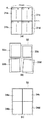
ここで、描画サイズについて、NANDフラッシュを例に挙げて説明する。図4(a)にNANDフラッシュのダイサイズと描画サイズとの関係を示す。ダイサイズは小さくなるにつれて1枚のシリコンウエハから多数のチップを製造でき、チップの製造原価は低下する。しかし、近年の記憶容量の増大とともにダイサイズは大きくなる傾向にある。最大描画サイズ(26mm×33mm)は、装置コストの増大を招かないように半導体業界で決定された上限値である。 Here, the drawing size will be described using a NAND flash as an example. FIG. 4A shows the relationship between the NAND flash die size and the drawing size. As the die size decreases, a large number of chips can be manufactured from one silicon wafer, and the manufacturing cost of the chips decreases. However, the die size tends to increase with the recent increase in storage capacity. The maximum drawing size (26 mm × 33 mm) is an upper limit value determined in the semiconductor industry so as not to increase the apparatus cost.
図4(b)にNANDフラッシュの画角内レイアウト例を示す。16GBのNANDフラッシュの場合、ダイサイズは142mm2となるため、最大描画サイズ内に6個配置でき、最大描画サイズの99%に収めることができる。一方、32GBのNANDフラッシュの場合では、最大描画サイズ内に4個しか配置できず、最大描画サイズの80%となるため、斜線部のエリアが余ってしまう。同様に、64GBのNANDフラッシュの場合でも、最大描画サイズ内に3個しか配置できず、最大描画サイズの85%となるため、斜線部のエリアが余ってしまう。複数の描画装置15を有する描画システム70では、このように描画サイズの異なるパターンを複数の描画装置15のそれぞれにおいて描画することが通常であり、全ての描画装置で最大描画サイズを描画することは稀である。
FIG. 4B shows a layout example within the field of view of the NAND flash. In the case of a 16 GB NAND flash, since the die size is 142 mm 2 , six pieces can be arranged within the maximum drawing size, and can be within 99% of the maximum drawing size. On the other hand, in the case of a 32 GB NAND flash, only four elements can be arranged within the maximum drawing size, which is 80% of the maximum drawing size, so that the shaded area remains. Similarly, even in the case of a 64 GB NAND flash, only three can be arranged within the maximum drawing size, which is 85% of the maximum drawing size, so that the hatched area remains. In the
図3において、第1描画装置15aでは最大描画サイズ(100%)のパターンを、第2描画装置15b及び第3描画装置15cでは最大描画サイズの75%のパターンを描画するものとする。最大描画サイズ(100%)のパターンを描画する第1描画装置15aのブランキング偏向器8aでは、第1補正部26a〜26dの全てを使って描画データの補正が行われる。一方、最大描画サイズの75%のパターンを描画する第2描画装置15b及び第3描画装置15cでは、最大描画サイズの75%の描画サイズを描画すればよいため、斜線で示した第1補正部27d及び28dは使用せず不要となる。このように、最大描画サイズよりも小さい描画サイズでパターンを描画する場合には、使用しない補正部が存在してしまい、無駄となってしまう。そのため、本発明の第1実施形態では、各描画装置(15a、15b又は15c)が描画する描画サイズに基づいて各描画装置(15a、15b又は15c)が必要とする個数の補正部を配分し、使用しない補正部を削減するようにしている。
In FIG. 3, the
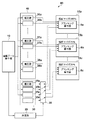
図1に、第1実施形態の描画システムにおけるデータ処理系のブロック図を示す。第1実施形態の描画システム60では、複数の描画装置15a、15b及び15cと第1補正処理部20とが配置されており、第1補正処理部20内には複数の第1補正部(第1処理部)26a〜28cが備えられている。従来の描画システム70と比べて、第1補正部27d及び28dが削除され、決定部29及び接続部30が新たに備えられている。
FIG. 1 shows a block diagram of a data processing system in the drawing system of the first embodiment. In the
第1実施形態における第1補正部26a〜28cは、各描画装置(15a、15b又は15c)に選択的に接続可能である。補正部の個数は、各描画装置(15a、15b又は15c)で描画するパターンの描画サイズの情報を事前に求めておけば、描画システム60全体で必要となる処理量が見積もられ、描画システム60全体で必要な補正部の個数を求めることができる。決定部29は、例えば、コンピュータなどの情報処理装置で構成され、各描画装置(15a、15b又は15c)に入力される描画データから、各描画装置(15a、15b又は15c)が基板13にパターンを描画する描画サイズを特定する。その特定した描画サイズに基づいて第1補正部(26a〜28c)のそれぞれと各描画装置(15a、15b又は15c)との接続関係を決定する。接続部30は入力ポートと出力ポートとの接続を切り替えるスイッチ回路を含み、決定部29で決定された接続関係に基づいて、第1補正部(26a〜28c)のそれぞれと各描画装置(15a、15b又は15c)とを接続する。
The 1st correction |
図1において、第1描画装置(第1描画ユニット)15aでは最大描画サイズ(100%)のパターンを、第2描画装置15b及び第3描画装置15cでは最大描画サイズの75%のパターンを描画するものとする。決定部29において、第1描画装置15aが基板13にパターンを描画する描画サイズに基づいて、第1描画装置15aのブランキング偏向器8aが必要とする補正部の個数を求める。この場合、第1描画装置15aでは最大描画サイズを描画するため、4個の補正部が必要である。この求めた補正部の個数に応じて、決定部29が複数の第1補正部(26a〜28c)から第1描画装置15aに接続する第1補正部を決定する。同様に、第2描画装置15a及び第3描画装置15cにおいても、それぞれの描画サイズに基づいて第2描画装置15b及び第3描画装置15cのブランキング偏向器8b及び8cが必要とする補正部の個数を求める。第2描画装置15b及び第3描画装置15cでは最大描画サイズの75%の描画サイズのパターンを描画するため3個の補正部が必要である。この求めた補正部の個数に応じて、決定部29が複数の第1補正部(26a〜28c)から第2描画装置15b及び第3描画装置15cに接続する第1補正部を決定する。接続部30では、決定部29の決定に基づいて、第1描画装置15aのブランキング偏向器8aには第1補正部26a〜26dを接続する。同様に、第2描画装置15bには第1補正部27a〜27cを、第3描画装置15cには第1補正部28a〜28cを接続する。このように、描画システム60では、各描画装置(15a、15b又は15c)が必要とする補正部の個数に応じて第1補正部26a〜28cを各描画装置(15a、15b又は15c)に接続することができる。これにより、描画システム60では、各描画装置で描画できる最大描画サイズのパターンを描画処理するために必要となる補正部の個数よりも少ない個数の第1補正部で第1補正処理部20を構成することができる。なお、各描画装置で描画できる最大描画サイズのパターンを描画処理するために必要となる補正部の個数とは、従来の描画システム70の第1補正処理部を構成する補正部の個数に相当する。これは、全ての描画装置で最大描画サイズを描画することは稀であるため、各描画装置で最低限必要となる第1補正部の個数の総和で第1補正処理部20を構成することができるからである。従って、描画システム60では、従来の描画システム70で最大描画サイズのパターンを描画しない限り不要となる補正部を削減することができる。換言すれば、描画システム60では、従来の描画システム70と比較して、コスト面などで有利な第1補正処理部20を構成することができる。なお、最大描画サイズ(100%)のみを描画する場合には、いくつかの描画装置の動作を停止させて、その分の補正部を動作している補正部に分配することで対応可能である。また、本実施形態における描画データは、ブランキング偏向器8を制御するブランキング制御部21に入力する制御データとして例示した。但し、描画データは、荷電粒子線4を基板上で走査するための偏向器11を制御する偏向制御部24に入力する制御データとして用いてもよい。
In FIG. 1, the first drawing device (first drawing unit) 15a draws a pattern of the maximum drawing size (100%), and the
補正部における具体的な処理内容を、荷電粒子線4を基板上で走査する偏向器11の補正を一例として説明する。図5(a)に最大描画サイズ(26mm×33mm)を4分割し、4本の荷電粒子線4で描画する例を示す。分割された荷電粒子線4のそれぞれには偏向器11が備えられており、偏向器11のそれぞれに補正部を割り当てて描画するものとする。荷電粒子線4のそれぞれは、偏向器11により矢印方向に繰り返し偏向され、基板13をステージ14で連続的に移動させることで分割された画角エリア31a〜31dのそれぞれを描画する。4本の荷電粒子線4にはそれぞれの収差により荷電粒子線4を照射すべき位置からの位置ずれがでるため、補正をかけずに描画すると図5(b)に示す補正前の描画パターン33a〜33dのように、点線で示した目標格子32に対して位置ずれを起こしてしまう。そこで、補正部のそれぞれでは、描画データに対して位置ずれ補正(シフト、回転)及び倍率補正(拡大、縮小)を行う。その結果、図5(c)に示す補正された描画パターン34a〜34dように、点線で示した目標格子32に沿って描画することができる。なお、補正には、近接効果補正やビーム強度補正などを追加してもよい。
<第2実施形態>
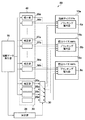
図6に、第2実施形態の描画システムにおけるデータ処理系のブロック図を示す。第2実施形態における描画システム80では、第1実施形態における描画システム60と比べて、第1補正処理部39の他に、第2補正処理部40が備えられている。第1補正処理部39には、各描画装置(15a、15b又は15c)に選択的に接続可能な第1補正部35a〜35dを有している。また、第2補正処理部40には、各描画装置(15a、15b又は15c)に固定的に接続する第2補正部(第2処理部)36a〜38bを有している。第2補正処理部40内の第2補正部36a〜38bは、一定の個数の補正部が各描画装置(15a、15b又は15c)のブランキング偏向器(8a、8b又は8c)に接続されるように、予め接続されている(図6の例では補正部を2個ずつ接続している)。一定の個数とは、各描画装置(15a、15b又は15c)で描画を予定している描画サイズの平均値などから決めることができる。ここで、一定の個数の第2補正部36a〜38bと各描画装置(15a、15b又は15c)との接続によって描画できる描画サイズを閾値として設定する。各描画装置(15a、15b又は15c)において描画データから特定される描画サイズ(即ち、描画領域の大きさ)が閾値(許容範囲)を超えるとき、第1補正処理部39内の第1補正部35a〜35dが、接続部30によって追加的に接続される。
A specific processing content in the correction unit will be described by taking as an example correction of the
Second Embodiment
FIG. 6 shows a block diagram of a data processing system in the drawing system of the second embodiment. The
図6において、第1描画装置15aでは最大描画サイズ(100%)のパターンを、第2描画装置15b及び第3描画装置15cでは最大描画サイズの75%のパターンを描画するものとする。決定部29において、描画データ発生器19から生成される描画データに基づいて、各描画装置(15a、15b又は15c)のブランキング偏向器8a、8b又は8cが必要とする補正部の個数を求める。この場合、第1描画装置15aでは最大描画サイズを描画するため4個の補正部が必要であり、第2描画装置15b及び第3描画装置15cでは最大描画サイズの75%の描画サイズであるため3個の補正部が必要である。第1描画装置15aでは、第2補正処理部40内の第2補正部36a及び36bが予め接続されているため、接続部30によって第1補正処理部39内の第1補正部35a及び35bを第1描画装置15aのブランキング偏向器8aに接続する。また、第2描画装置15bでは、第2補正処理部40内の第2補正部37a及び37bが予め接続されているため、接続部30によって第1補正処理部39内の第1補正部35cを第2描画装置15bのブランキング偏向器8bに接続する。同様に、第1補正部35dを第3描画装置15cのブランキング偏向器8cに接続する。このように、描画システム80では、各描画装置(15a、15b又は15c)が必要とする補正部の個数に応じて、第2補正部(36a〜38b)だけでは不足となる補正部の個数を描画装置ごとに求める。そして、不足となる補正部の個数に応じて、第1補正部35a〜35dを各描画装置(15a、15b又は15c)に接続する。従って、描画システム80においても、第1の実施形態と同様の効果を得ることができる。即ち、第1補正部の個数と第2補正部の個数との総数が、各描画装置で描画できる最大描画サイズのパターンを描画処理するために必要となる補正部の個数よりも少なくなるように、第1補正処理部39及び第2補正処理部40を構成することができる。
In FIG. 6, the
次に、各描画装置(15a、15b又は15c)における描画サイズが変更された場合の例を示す。図6の例では、第1描画装置15a、第2描画装置15b及び第3描画装置15cの描画サイズはそれぞれ100%、75%及び75%であった。これらの描画サイズがそれぞれ50%、100%及び100%に変更した場合を図7に示す。この場合、第1描画装置15aでは最大描画サイズの50%の描画サイズであるため2個の補正部が必要であり、第2描画装置15b及び第3描画装置15cでは最大描画サイズを描画するため4個の補正部が必要である。第1描画装置15aでは、第2補正処理部40内の第2補正部36a及び36bが予め接続されているため、第1補正処理部39から第1補正部を接続する必要はない。一方で、第2描画装置15b及び第3描画装置15cでは、第2補正処理部40内の第2補正部が2個しか接続されていない。そのため、第1補正処理部39内の第1補正部35a及び35bを第2描画装置15bのブランキング偏向器8bに接続し、第1補正部35c及び35dを第3描画装置15cのブランキング偏向器8cに接続する。このように、第2実施形態の描画システム80では、各描画装置(15a、15b又は15c)の描画サイズが変更しても、第1補正処理部39内の第1補正部35a〜35dを切り替えることで柔軟に対処することができる。
Next, an example in which the drawing size in each drawing apparatus (15a, 15b, or 15c) is changed will be described. In the example of FIG. 6, the drawing sizes of the
ここで、接続部30について説明する。図8(a)に第2実施形態における接続部の周辺ブロック図を示す。第2実施形態の接続部30では、4個の第1補正部に対して6個の接続先があるため、図8(a)に示すような4入力6出力のスイッチ回路が必要である。このスイッチ回路の具体的な例を、図8(b)及び(c)に示す。
Here, the
図8(b)に示すスイッチ回路41は、スイッチ素子42と同軸コネクタ43とメタルケーブル44とで構成されている。このようなスイッチ回路41は、主に入力ポート(IN)からの信号(本実施形態では、描画データ)の通信速度が低速であるときに用いられる。スイッチ素子42は、多入力多出力の電気信号に対応しており、比較的安価に市販されている。
The
図8(c)に示すスイッチ回路45は、光スイッチ素子46と光コネクタ48と光ファイバー49とで構成されている。このようなスイッチ回路45は、主に入力ポート(IN)からの信号(本実施形態では、描画データ)の通信速度が高速であるときに用いられる。光スイッチ素子46では、入力ポート(IN)から入力された光信号の反射角度を反射ミラー47によって制御し、所定の出力ポート(OUT)に導光される。近年の光MEMS(Micro Electro Mechanical System)技術の進展により、高密度な反射ミラー47を作製できるため、大規模であった光スイッチ素子46をコンパクトにできる。
<物品の製造方法の実施形態>
本発明の実施形態にかける物品の製造方法は、例えば、半導体デバイス等のマイクロデバイスや微細構造を有する素子等の物品を製造するのに好適である。本実施形態の物品の製造方法は、基板に塗布された感光剤に上記の描画装置を用いて潜像パターンを形成する工程(基板に描画を行う工程)と、かかる工程で潜像パターンが形成された基板を現像する工程とを含む。更に、かかる製造方法は、他の周知の工程(酸化、成膜、蒸着、ドーピング、平坦化、エッチング、レジスト剥離、ダイシング、ボンディング、パッケージング等)を含む。本実施形態の物品の製造方法は、従来の方法に比べて、物品の性能・品質・生産性・生産コストの少なくとも1つにおいて有利である。
The
<Embodiment of Method for Manufacturing Article>
The method for manufacturing an article according to an embodiment of the present invention is suitable for manufacturing an article such as a microdevice such as a semiconductor device or an element having a fine structure. In the method for manufacturing an article according to the present embodiment, a latent image pattern is formed on the photosensitive agent applied to the substrate by using the above drawing apparatus (a step of drawing on the substrate), and the latent image pattern is formed by such a step. Developing the processed substrate. Further, the manufacturing method includes other well-known steps (oxidation, film formation, vapor deposition, doping, planarization, etching, resist stripping, dicing, bonding, packaging, and the like). The method for manufacturing an article according to the present embodiment is advantageous in at least one of the performance, quality, productivity, and production cost of the article as compared with the conventional method.
以上、本発明の好ましい実施形態について説明したが、本発明はこれらの実施形態に限定されないことはいうまでもなく、その要旨の範囲内で種々の変形及び変更が可能である。 As mentioned above, although preferable embodiment of this invention was described, it cannot be overemphasized that this invention is not limited to these embodiment, A various deformation | transformation and change are possible within the range of the summary.
Claims (7)
前記複数の描画ユニットそれぞれに選択的に接続可能な複数の第1処理部と、
前記複数の描画ユニットの中の第1描画ユニットに接続する第1処理部を前記複数の第1処理部の中から描画データに基づいて決定する決定部と、
前記決定部で決定された第1処理部と前記第1描画ユニットとを接続する接続部と、
を有することを特徴とする描画装置。 A drawing apparatus having a plurality of drawing units for drawing on a substrate with a charged particle beam,
A plurality of first processing units selectively connectable to each of the plurality of drawing units;
A determination unit for determining a first processing unit connected to a first drawing unit among the plurality of drawing units from the plurality of first processing units based on drawing data;
A connection unit that connects the first processing unit determined by the determination unit and the first drawing unit;
A drawing apparatus comprising:
前記決定部は、前記描画領域の大きさが前記複数の第2処理部での許容範囲を超える場合に、前記第1描画ユニットに接続する前記第1処理部を決定する、ことを特徴とする請求項2に記載の描画装置。 A plurality of second processing units respectively connected to the plurality of drawing units;
The determining unit determines the first processing unit to be connected to the first drawing unit when the size of the drawing area exceeds an allowable range of the plurality of second processing units. The drawing apparatus according to claim 2.
前記描画データは、前記偏向器のための制御データである、ことを特徴とする請求項1乃至3のうちいずれか1項に記載の描画装置。 A deflector for blanking the charged particle beam;
The drawing apparatus according to claim 1, wherein the drawing data is control data for the deflector.
前記描画データは、前記偏向器のための制御データである、ことを特徴とする請求項1乃至3のうちいずれか1項に記載の描画装置。 A deflector that scans the charged particle beam on the substrate;
The drawing apparatus according to claim 1, wherein the drawing data is control data for the deflector.
前記工程で描画が行われた前記基板を現像する工程と、
を有することを特徴とする物品の製造方法。 Drawing on a substrate using the drawing apparatus according to any one of claims 1 to 5,
Developing the substrate on which the drawing has been performed in the step;
A method for producing an article comprising:
前記描画装置は、前記複数の描画ユニットそれぞれに選択的に接続可能な複数の第1処理部を有するものであり、
前記複数の描画ユニットの中の第1描画ユニットに接続する第1処理部を前記複数の第1処理部の中から描画データに基づいて決定する処理を行う、
ことを特徴とする処理装置。 A processing apparatus connected to a drawing apparatus having a plurality of drawing units for drawing on a substrate with a charged particle beam,
The drawing apparatus includes a plurality of first processing units that can be selectively connected to the plurality of drawing units,
A process of determining a first processing unit connected to a first drawing unit among the plurality of drawing units from the plurality of first processing units based on drawing data;
The processing apparatus characterized by the above-mentioned.
Priority Applications (2)
| Application Number | Priority Date | Filing Date | Title |
|---|---|---|---|
| JP2012002476A JP2013143451A (en) | 2012-01-10 | 2012-01-10 | Drawing device, and manufacturing method and processing device of article |
| US13/734,192 US8618497B2 (en) | 2012-01-10 | 2013-01-04 | Drawing apparatus, method of manufacturing article, and information processing apparatus |
Applications Claiming Priority (1)
| Application Number | Priority Date | Filing Date | Title |
|---|---|---|---|
| JP2012002476A JP2013143451A (en) | 2012-01-10 | 2012-01-10 | Drawing device, and manufacturing method and processing device of article |
Publications (2)
| Publication Number | Publication Date |
|---|---|
| JP2013143451A true JP2013143451A (en) | 2013-07-22 |
| JP2013143451A5 JP2013143451A5 (en) | 2015-02-26 |
Family
ID=48743272
Family Applications (1)
| Application Number | Title | Priority Date | Filing Date |
|---|---|---|---|
| JP2012002476A Pending JP2013143451A (en) | 2012-01-10 | 2012-01-10 | Drawing device, and manufacturing method and processing device of article |
Country Status (2)
| Country | Link |
|---|---|
| US (1) | US8618497B2 (en) |
| JP (1) | JP2013143451A (en) |
Families Citing this family (1)
| Publication number | Priority date | Publication date | Assignee | Title |
|---|---|---|---|---|
| JP5927067B2 (en) * | 2012-07-06 | 2016-05-25 | 株式会社日立ハイテクノロジーズ | Measurement inspection apparatus and measurement inspection method |
Citations (3)
| Publication number | Priority date | Publication date | Assignee | Title |
|---|---|---|---|---|
| JPH06216014A (en) * | 1993-01-13 | 1994-08-05 | Hitachi Ltd | Electron beam lithography device |
| JPH09330871A (en) * | 1996-06-12 | 1997-12-22 | Canon Inc | Electron beam exposing system and method for manufacturing device using the same |
| JPH10163081A (en) * | 1996-11-29 | 1998-06-19 | Hitachi Ltd | Electron beam drawing system and its method and semiconductor device using the same |
Family Cites Families (2)
| Publication number | Priority date | Publication date | Assignee | Title |
|---|---|---|---|---|
| JP5873275B2 (en) * | 2011-09-12 | 2016-03-01 | キヤノン株式会社 | Drawing apparatus and article manufacturing method |
| JP5848135B2 (en) * | 2012-01-10 | 2016-01-27 | 株式会社ニューフレアテクノロジー | Charged particle beam drawing method, charged particle beam drawing program, and charged particle beam drawing apparatus |
-
2012
- 2012-01-10 JP JP2012002476A patent/JP2013143451A/en active Pending
-
2013
- 2013-01-04 US US13/734,192 patent/US8618497B2/en not_active Expired - Fee Related
Patent Citations (3)
| Publication number | Priority date | Publication date | Assignee | Title |
|---|---|---|---|---|
| JPH06216014A (en) * | 1993-01-13 | 1994-08-05 | Hitachi Ltd | Electron beam lithography device |
| JPH09330871A (en) * | 1996-06-12 | 1997-12-22 | Canon Inc | Electron beam exposing system and method for manufacturing device using the same |
| JPH10163081A (en) * | 1996-11-29 | 1998-06-19 | Hitachi Ltd | Electron beam drawing system and its method and semiconductor device using the same |
Also Published As
| Publication number | Publication date |
|---|---|
| US8618497B2 (en) | 2013-12-31 |
| US20130175453A1 (en) | 2013-07-11 |
Similar Documents
| Publication | Publication Date | Title |
|---|---|---|
| US6107636A (en) | Electron beam exposure apparatus and its control method | |
| EP1253619B1 (en) | Charged particle beam exposure apparatus and device manufacturing method using same | |
| JP5634052B2 (en) | Charged particle beam drawing apparatus and device manufacturing method | |
| JP5744564B2 (en) | Drawing apparatus, drawing method, and article manufacturing method | |
| US20050199827A1 (en) | Charged particle beam apparatus, charged particle beam control method, substrate inspection method and method of manufacturing semiconductor device | |
| JP6589758B2 (en) | Multi-charged particle beam writing apparatus and multi-charged particle beam writing method | |
| JPH09245708A (en) | Electron beam exposure device and exposure method thereof | |
| JP2013074088A (en) | Charged particle ray drawing device, drawing data generation method, drawing data generating program, and method of manufacturing article using the same | |
| US10211023B2 (en) | Aperture set for multi-beam and multi-charged particle beam writing apparatus | |
| JPH1187206A (en) | Electron beam aligner and manufacture of device using the same | |
| JP2015070213A (en) | Lithography system, and method of manufacturing article | |
| US8686374B2 (en) | Drawing apparatus, and method of manufacturing article | |
| JP2013143451A (en) | Drawing device, and manufacturing method and processing device of article | |
| TW202042270A (en) | Multi charged particle beam writing apparatus | |
| JP4018197B2 (en) | Electron beam exposure method and electron beam exposure apparatus | |
| JP4955433B2 (en) | Deflector array, exposure apparatus, and device manufacturing method | |
| JP2014082171A (en) | Irradiation system, drawing device and method of manufacturing article | |
| JP2005032837A (en) | Method for charged particle beam lithography and method of manufacturing device using the same | |
| JP2016096270A (en) | Blanking system for multi charged particle beam, and multi charged particle beam lithography device | |
| JP4477436B2 (en) | Charged particle beam exposure system | |
| JP2015035563A (en) | Drawing data generation method, processing device, program, drawing device and article manufacturing method | |
| JP2005101668A (en) | Electron beam exposure device and its exposuring method | |
| JPH11195589A (en) | Multiple electron beam exposure method and its apparatus, and manufacture of device | |
| CN108227395B (en) | Photoetching system and method for enhancing image contrast and writing integrated circuit pattern | |
| US20150037731A1 (en) | Drawing apparatus and article manufacturing method |
Legal Events
| Date | Code | Title | Description |
|---|---|---|---|
| A521 | Request for written amendment filed |
Free format text: JAPANESE INTERMEDIATE CODE: A523 Effective date: 20150113 |
|
| A621 | Written request for application examination |
Free format text: JAPANESE INTERMEDIATE CODE: A621 Effective date: 20150113 |
|
| A977 | Report on retrieval |
Free format text: JAPANESE INTERMEDIATE CODE: A971007 Effective date: 20151007 |
|
| A131 | Notification of reasons for refusal |
Free format text: JAPANESE INTERMEDIATE CODE: A131 Effective date: 20151013 |
|
| A02 | Decision of refusal |
Free format text: JAPANESE INTERMEDIATE CODE: A02 Effective date: 20160226 |