JP5744564B2 - Drawing apparatus, drawing method, and article manufacturing method - Google Patents
Drawing apparatus, drawing method, and article manufacturing method Download PDFInfo
- Publication number
- JP5744564B2 JP5744564B2 JP2011040270A JP2011040270A JP5744564B2 JP 5744564 B2 JP5744564 B2 JP 5744564B2 JP 2011040270 A JP2011040270 A JP 2011040270A JP 2011040270 A JP2011040270 A JP 2011040270A JP 5744564 B2 JP5744564 B2 JP 5744564B2
- Authority
- JP
- Japan
- Prior art keywords
- substrate
- charged particle
- particle beams
- pattern
- drawing apparatus
- Prior art date
- Legal status (The legal status is an assumption and is not a legal conclusion. Google has not performed a legal analysis and makes no representation as to the accuracy of the status listed.)
- Expired - Fee Related
Links
Images


Classifications
-
- H—ELECTRICITY
- H01—ELECTRIC ELEMENTS
- H01J—ELECTRIC DISCHARGE TUBES OR DISCHARGE LAMPS
- H01J37/00—Discharge tubes with provision for introducing objects or material to be exposed to the discharge, e.g. for the purpose of examination or processing thereof
- H01J37/30—Electron-beam or ion-beam tubes for localised treatment of objects
- H01J37/317—Electron-beam or ion-beam tubes for localised treatment of objects for changing properties of the objects or for applying thin layers thereon, e.g. for ion implantation
- H01J37/3174—Particle-beam lithography, e.g. electron beam lithography
-
- H—ELECTRICITY
- H01—ELECTRIC ELEMENTS
- H01J—ELECTRIC DISCHARGE TUBES OR DISCHARGE LAMPS
- H01J37/00—Discharge tubes with provision for introducing objects or material to be exposed to the discharge, e.g. for the purpose of examination or processing thereof
- H01J37/02—Details
- H01J37/04—Arrangements of electrodes and associated parts for generating or controlling the discharge, e.g. electron-optical arrangement, ion-optical arrangement
- H01J37/045—Beam blanking or chopping, i.e. arrangements for momentarily interrupting exposure to the discharge
-
- B—PERFORMING OPERATIONS; TRANSPORTING
- B82—NANOTECHNOLOGY
- B82Y—SPECIFIC USES OR APPLICATIONS OF NANOSTRUCTURES; MEASUREMENT OR ANALYSIS OF NANOSTRUCTURES; MANUFACTURE OR TREATMENT OF NANOSTRUCTURES
- B82Y10/00—Nanotechnology for information processing, storage or transmission, e.g. quantum computing or single electron logic
-
- B—PERFORMING OPERATIONS; TRANSPORTING
- B82—NANOTECHNOLOGY
- B82Y—SPECIFIC USES OR APPLICATIONS OF NANOSTRUCTURES; MEASUREMENT OR ANALYSIS OF NANOSTRUCTURES; MANUFACTURE OR TREATMENT OF NANOSTRUCTURES
- B82Y40/00—Manufacture or treatment of nanostructures
-
- H—ELECTRICITY
- H01—ELECTRIC ELEMENTS
- H01J—ELECTRIC DISCHARGE TUBES OR DISCHARGE LAMPS
- H01J37/00—Discharge tubes with provision for introducing objects or material to be exposed to the discharge, e.g. for the purpose of examination or processing thereof
- H01J37/30—Electron-beam or ion-beam tubes for localised treatment of objects
- H01J37/317—Electron-beam or ion-beam tubes for localised treatment of objects for changing properties of the objects or for applying thin layers thereon, e.g. for ion implantation
- H01J37/3174—Particle-beam lithography, e.g. electron beam lithography
- H01J37/3177—Multi-beam, e.g. fly's eye, comb probe
-
- H—ELECTRICITY
- H01—ELECTRIC ELEMENTS
- H01J—ELECTRIC DISCHARGE TUBES OR DISCHARGE LAMPS
- H01J2237/00—Discharge tubes exposing object to beam, e.g. for analysis treatment, etching, imaging
- H01J2237/04—Means for controlling the discharge
- H01J2237/043—Beam blanking
- H01J2237/0435—Multi-aperture
-
- H—ELECTRICITY
- H01—ELECTRIC ELEMENTS
- H01J—ELECTRIC DISCHARGE TUBES OR DISCHARGE LAMPS
- H01J2237/00—Discharge tubes exposing object to beam, e.g. for analysis treatment, etching, imaging
- H01J2237/30—Electron or ion beam tubes for processing objects
- H01J2237/317—Processing objects on a microscale
- H01J2237/3175—Lithography
- H01J2237/31761—Patterning strategy
- H01J2237/31764—Dividing into sub-patterns
-
- H—ELECTRICITY
- H01—ELECTRIC ELEMENTS
- H01J—ELECTRIC DISCHARGE TUBES OR DISCHARGE LAMPS
- H01J2237/00—Discharge tubes exposing object to beam, e.g. for analysis treatment, etching, imaging
- H01J2237/30—Electron or ion beam tubes for processing objects
- H01J2237/317—Processing objects on a microscale
- H01J2237/3175—Lithography
- H01J2237/31761—Patterning strategy
- H01J2237/31766—Continuous moving of wafer
Landscapes
- Chemical & Material Sciences (AREA)
- Engineering & Computer Science (AREA)
- Nanotechnology (AREA)
- Analytical Chemistry (AREA)
- Physics & Mathematics (AREA)
- Crystallography & Structural Chemistry (AREA)
- Condensed Matter Physics & Semiconductors (AREA)
- General Physics & Mathematics (AREA)
- Manufacturing & Machinery (AREA)
- Mathematical Physics (AREA)
- Theoretical Computer Science (AREA)
- Electron Beam Exposure (AREA)
Description
本発明は、複数の荷電粒子線で基板上にパターンを描画する描画装置および描画方法に関する。 The present invention relates to a drawing apparatus and a drawing method for drawing a pattern on a substrate with a plurality of charged particle beams.
フォトリソグラフィ技術において、最小パターン寸法が光源の波長に近づくと、意図しない光の相互作用(干渉)により、所望のパターンとは異なったパターンで基板の露光が行われうる。光近接効果補正を適用しても、所望のパターンが微細化して光の相互作用がより複雑になるのに従って、十分な補正が困難となっている。
このような問題を解決するため、パターンの幅を一定にし、かつ、その長手方向を限定したデバイスデザインルール(以後、1Dレイアウトと呼ぶ)や、そのための加工方法が提案されている(非特許文献1)。
In the photolithography technique, when the minimum pattern dimension approaches the wavelength of the light source, the substrate can be exposed in a pattern different from the desired pattern due to unintended light interaction (interference). Even if the optical proximity effect correction is applied, sufficient correction becomes difficult as the desired pattern becomes finer and the light interaction becomes more complicated.
In order to solve such a problem, a device design rule (hereinafter referred to as 1D layout) in which the pattern width is constant and the longitudinal direction thereof is limited, and a processing method therefor have been proposed (non-patent document). 1).
図10を参照して当該加工方法を説明する。この方法は、22nm世代のSRAMのゲートセルを対象として液浸露光装置(光源波長は193nm)を用いて行うフォトリソグラフィプロセスに関するものである。そのステップを以下に述べる。
[ステップ1] 44nmハーフピッチのラインアンドスペースパターンの露光を行う。
[ステップ2] 現像して形成したパターンに対して直接(あるいは、下地を加工し、全面に等方的に成膜した後に)異方性エッチングを行って、パターンの側壁、すなわち、輪郭に膜を残す。その結果、22nmハーフピッチのラインアンドスペースのハードマスクを得る。いわゆる、サイドウォールを利用したダブルパターニング技術である。
[ステップ3] レジストを塗布し、カット用のホールパターンの露光を行う。
[ステップ4] 露光されたホールパターン領域を化学的処理により縮小する。
[ステップ5] 再度異方性エッチングすることにより、所望のゲートセルパターンのハードマスクを得る。
The processing method will be described with reference to FIG. This method relates to a photolithography process performed using an immersion exposure apparatus (light source wavelength: 193 nm) for a 22-nm generation SRAM gate cell. The steps are described below.
[Step 1] A 44 nm half pitch line and space pattern is exposed.
[Step 2] The pattern formed by development is subjected to anisotropic etching directly (or after the base is processed and isotropically formed on the entire surface) to form a film on the side wall of the pattern, that is, on the contour. Leave. As a result, a 22 nm half pitch line and space hard mask is obtained. This is a so-called double patterning technology using a sidewall.
[Step 3] A resist is applied, and a hole pattern for cutting is exposed.
[Step 4] The exposed hole pattern region is reduced by chemical treatment.
[Step 5] By performing anisotropic etching again, a hard mask having a desired gate cell pattern is obtained.
上記方法は、液浸露光装置を使用してもダブルパターニング技術を適用しなくてはならず、また、カット用ホールパターンの露光も難しいため、[ステップ4]のようなパターン縮小工程が必要となっている。マスク数や工程数も多く、フォトリソグラフィプロセスのコスト高や信頼性低下が問題となっている。 In the above method, even if an immersion exposure apparatus is used, the double patterning technique must be applied, and it is difficult to expose the hole pattern for cutting. Therefore, a pattern reduction process such as [Step 4] is required. It has become. The number of masks and the number of processes are also large, and the high cost of the photolithography process and the decrease in reliability are problems.
本発明は、上述のデザインルールのパターンを描画する信頼性およびスループットの点で有利な描画装置を提供することを例示的目的とする。 An object of the present invention is to provide a drawing apparatus that is advantageous in terms of reliability and throughput in drawing the pattern of the above-described design rule.
本発明の一つの側面は、複数の荷電粒子線で基板に描画を行う描画装置であって、
前記複数の荷電粒子線それぞれの前記基板上でのサイズを規定する開口を有するアパーチャアレイ部材と、
前記複数の荷電粒子線を個別にブランキングするブランカアレイと、
互いに交差する第1方向および第2方向それぞれにおいて前記複数の荷電粒子線と前記基板との間の相対走査を行うことにより前記複数の荷電粒子線と前記基板との間のラスター走査を行う走査手段と、
前記ラスター走査に並行して、前記基板上において、前記第1方向および前記第2方向のうちの少なくとも一つに関して、前記複数の荷電粒子線のピッチより小さい所定ピッチをもって前記ブランカアレイによるブランキングを制御する制御手段と、を有し、
前記サイズおよび前記所定ピッチは、前記第1方向および前記第2方向のうちの前記少なくとも一つのうちの一つにおいてより前記第1方向および前記第2方向のうちの他の一つにおいての方が小さい、ことを特徴とする描画装置である。
One aspect of the present invention is a drawing apparatus for drawing on a substrate with a plurality of charged particle beams,
An aperture array member having an opening for defining a size of each of the plurality of charged particle beams on the substrate;
A blanker array for individually blanking the plurality of charged particle beams;
Scanning means for performing raster scanning between the plurality of charged particle beams and the substrate by performing relative scanning between the plurality of charged particle beams and the substrate in each of a first direction and a second direction intersecting each other. When,
Wherein in parallel to the raster scan, in the substrate, for at least one of said first and second directions, blanking by the blanker array with a smaller predetermined pitch than the pitch of the plurality of charged particle beams Control means for controlling ranking , and
The size and the predetermined pitch, the direction of the other one of said first direction and said more the first direction and the second direction in one one of the at least one of the second direction A drawing apparatus characterized by being small.
本発明によれば、上述のデザインルールのパターンを描画する信頼性およびスループットの点で有利な描画装置を提供することができる。 According to the present invention, it is possible to provide a drawing apparatus that is advantageous in terms of reliability and throughput for drawing the above-described design rule pattern.
以下、添付図面を参照して本発明の実施形態を説明する。なお、実施形態を説明するための全図を通して、原則として、同一の部材等には同一の符号を付し、その繰り返しの説明は省略する。 Embodiments of the present invention will be described below with reference to the accompanying drawings. Note that, throughout the drawings for explaining the embodiments, in principle, the same members and the like are denoted by the same reference numerals, and repeated description thereof is omitted.
[実施形態1]
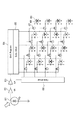
図1は、描画装置の構成を示す図である。図1において、1は、電子源であり、電子放出材としてLaB6またはBaO/W(ディスペンサーカソード)などを含むいわゆる熱電子型の電子源を用いうる。2は、コリメータレンズで、電界により電子ビームを収束させる静電型のレンズを用いうる。電子源1から放射された電子ビーム(電子線)は、コリメータレンズ2によって略平行の電子ビームとなる。なお、実施形態1および2の描画装置は、複数の電子線で基板上にパターンを描画するものであるが、イオン線等の電子線以外の荷電粒子線を用いてもよく、複数の荷電粒子線で基板上にパターンを描画する描画装置に一般化しうるものである。
[Embodiment 1]
FIG. 1 is a diagram illustrating a configuration of a drawing apparatus. In FIG. 1,
3は、2次元に配列された開口を有するアパーチャアレイ(アパーチャアレイ部材)である。4は、同一の光学的パワーを有する静電型のコンデンサーレンズが2次元に配列されたコンデンサーレンズアレイである。5は、電子ビームの形状を規定する(決める)パターン開口のアレイ(サブアレイ)を各コンデンサーレンズに対応して含むパターン開口アレイ(アパーチャアレイ部材)である。5aは、当該サブアレイを上から見た形状を示す。
コリメータレンズ2からの略平行な電子ビームは、アパーチャアレイ3によって複数の電子ビームに分割される。分割された電子ビームは、対応するコンデンサーレンズアレイ4のコンデンサーレンズを介して、対応するパターン開口アレイ5のサブアレイを照明する。ここで、アパーチャアレイ3は、当該照明の範囲を規定する機能を有している。
The substantially parallel electron beam from the
6は、個別に駆動可能な静電型のブランカー(電極対)を各コンデンサーレンズに対応して配列してなるブランカーアレイである。7は、ブランキングアパーチャ(1つの開口)を各コンデンサーレンズに対応して配列してなるブランキングアパーチャアレイである。8は、電子ビームを所定の方向に偏向させる偏向器を各コンデンサーレンズに対応して配列してなる偏向器アレイである。9は、静電型の対物レンズが各コンデンサーレンズに対応して配列されてなる対物レンズアレイである。10は、描画(露光)を行われるウエハ(基板)である。ここで、符号1−7および9の構成要素は、投影系を構成している。
電子ビームで照明されたパターン開口アレイ5の各サブアレイからの電子ビームは、それに対応するブランカー・ブランキングアパーチャ・偏向器・対物レンズを介して、100分の1の大きさに縮小されてウエハ10に投影される。ここで、サブアレイにおいてパターン開口の配列されている面が物面であり、かつ、ウエハ10の上面が像面である、という関係となっている。
The electron beam from each sub-array of the
また、電子ビームで照明されたパターン開口アレイ5のサブアレイからの電子ビームは、それに対応するブランカーの制御により、ブランキングアパーチャにより遮断されるか否か、すなわち、ウエハに電子線が入射するか否かが切り替えられる。それと並行して、ウエハに入射する電子線は、偏向器アレイ8により、同一の偏向量でウエハ上を走査される。
Further, whether or not the electron beam from the sub-array of the
また、電子源1は、コリメータレンズ2とコンデンサーレンズとを介してブランキングアパーチャ上に結像され、その像の大きさは、ブランキングアパーチャの開口より大きくなるように設定されている。このため、ウエハ上の電子ビームのセミアングル(半角)は、ブランキングアパーチャの開口により規定される。さらに、ブランキングアパーチャの開口は、それに対応する対物レンズの前側焦点位置に配置されているため、サブアレイの複数のパターン開口からの複数の電子ビームの主光線は、ウエハ上に略垂直に入射する。このため、ウエハ10の上面が上下に変位しても、水平面内での電子ビームの変位は微小となる。
The
11は、ウエハ10を保持し、光軸と直交するX−Y平面(水平面)内で可動なX−Yステージ(単にステージともいう)である。ステージは、ウエハ10を保持する(引きつける)ための静電チャック(不図示)と、電子ビームが入射する開口パターンを含み、電子ビームの位置を検出する検出器(不図示)とを含んでいる。12は、ウエハ10を搬送し、ステージ11との間でウエハ10の受け渡しを行う搬送機構である。
ブランキング制御回路13は、ブランカーアレイ6を構成する複数のブランカーを個別に制御する制御回路である。偏向器制御回路14は、偏向器アレイ8を構成する複数の偏向器を共通の信号で制御する制御回路である。ステージ制御回路15、ステージの位置を計測する不図示のレーザ干渉計と協働してステージ11の位置決めを制御する制御回路である主制御系16は、上記の複数の制御回路を制御し、描画装置を統括的に制御する。なお、描画装置の制御手段は、本実施形態では制御回路13−15および主制御系16により構成されているが、これは一例に過ぎず、適宜変更が可能である。
The blanking
図2は、ブランカーアレイ6の構成を示す図である。ブランキング制御回路13から制御信号は、光通信用光ファイバー(不図示)を介してブランカーアレイ6に供給される。1ファイバー当たり、1サブアレイに対応した複数のブランカーの制御信号を伝送する。光通信用光ファイバーから光信号は、フォトダイオード61で受光され、トランスファーインピーダンスアンプ62で電流−電圧変換され、リミッティングアンプ63で振幅調整される。振幅調整された信号がシフトレジスタ64に入力され、シリアル信号がパラレル信号に変換される。横方向に走るゲート電極線と縦方向に走るソース電極線との各交点には、FET67が配置され、FET67のゲートとソースとに2本のバス線がそれぞれ接続されている。FET67のドレインにはブランカー電極69およびコンデンサー68が接続され、これら2つの容量性素子の反対側は共通電極(コモン電極)に接続されている。ゲート電極線に加えられた電圧によって、それに接続されている1行分すべてのFETがON動作することで、ソース−ドレイン間に電流が流れる。そのときソース電極線に加えられている各々の電圧がブランカー電極69に印加され、その電圧に応じた電荷がコンデンサー68に蓄積(充電)される。ゲート電極線は、1行分の充電を終えると切り替えられ、電圧の印加は次の行に移り、最初の1行分のFETは、ゲート電圧を失ってOFF動作をする。最初の1行分のブランカー電極69は、ソース電極線からの電圧を失うが、コンデンサー68に蓄積された電荷によって、次にゲート電極線に電圧が印加されるまでの間は必要な電圧を維持できるようになっている。このようにFETをスイッチとして使ったアクティブ・マトリクス駆動方式によれば、ゲート電極線によって並行して多数のFETに電圧を印加することができるため、ブランカーの多数化に少ない配線数で対応できる。
FIG. 2 is a diagram showing a configuration of the
図2の例では、ブランカーは、4行4列に配列されている。シフトレジスタ64からのパラレル信号は、データドライバー65・ソース電極を介して、FETのソース電極に電圧として印加される。これと協働して、ゲートドライバー66から印加される電圧により、1行分のFETがON動作とされるため、対応する1行分のブランカーが制御される。このような動作が各行に対して順次繰り返されて、4行4列のブランカーが制御される。
In the example of FIG. 2, the blankers are arranged in 4 rows and 4 columns. The parallel signal from the
図3を参照しながら、本実施形態に係るラスター走査式の描画方法を説明する。電子ビームは、偏向器アレイ8による偏向とステージ11の位置とで決定されるウエハ10上の走査グリッド上を走査されながら、描画パターンPに応じて、基板上への照射・非照射がブランカーアレイ6により制御される。ここで、走査グリッドとは、図3に示すように、X方向にピッチGX(第1間隔)、Y方向にピッチGY(第2間隔)で形成されるグリッドである。そして、図中の縦線と横線との交点(グリッド点)に、電子ビームの照射または非照射が割り当てられるものである。
A raster scanning drawing method according to the present embodiment will be described with reference to FIG. While the electron beam is scanned on the scanning grid on the
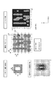
図4は、ウエハ上での電子線サブアレイの配置および走査を説明する図である。図4に示すように、サブアレイのパターン開口は、X方向にピッチBXで、Y方向にピッチBYで、ウエハ上に投影される。各パターン開口の大きさは、ウエハ上で、X方向はPXで、Y方向PYである。パターン開口は、ウエハに100分の1に縮小投影されるため、その実際の大きさは、ウエハ上での大きさの100倍である。パターン開口の像(電子ビーム)は、偏向器アレイ8によりX方向に偏向されて、ウエハ上で走査される。それと並行して、ステージ11はY方向に連続的に移動して(走査させて)いる。そこで、ウエハ10上において各電子ビームがY方向には静止しているように、偏向器アレイ8により電子ビームをY方向に偏向している。なお、投影系により投影される荷電粒子線を少なくともX方向(第1方向)に偏向させる偏向器アレイ8と、基板を保持してY方向(第1方向と直交する第2方向)に可動のステージ11は、走査手段に含まれる。ここで、走査手段は、X方向およびY方向において複数の荷電粒子線と基板との間の相対走査を行う手段である。
FIG. 4 is a diagram for explaining the arrangement and scanning of the electron beam sub-array on the wafer. As shown in FIG. 4, the pattern openings in the subarray are projected onto the wafer at a pitch BX in the X direction and at a pitch BY in the Y direction. The size of each pattern opening is PX in the X direction and Y direction PY on the wafer. Since the pattern aperture is reduced and projected to 1/100 on the wafer, its actual size is 100 times the size on the wafer. The image of the pattern aperture (electron beam) is deflected in the X direction by the
図5は、ウエハ上での電子ビームの走査の軌跡を示す図である。図5において、左側は、サブアレイの各電子ビームのX方向における走査の軌跡を示す。ここで、各電子ビームの照射・非照射は、グリッドピッチGXで規定されるグリッド点ごとに制御される。ここでは、説明を容易にするため、最上部の電子ビームの軌跡を黒塗りにしている。図5において、右側は、各電子ビームのX方向の走査のあと、破線の矢印で示すようなY方向の偏向幅DPでのフライバックを介して、各電子ビームのX方向の走査を順次繰り返して形成される軌跡を示す。図中の太破線枠内では、ストライプ幅SWのストライプ描画領域SAがグリッドピッチGYで埋め尽くされるのが分かる。すなわち、ストライプ描画領域SAは、ステージ11の定速連続移動で描画できることになる。そのための条件は、サブアレイのビーム本数をN*Nとすると、
N2=K*L+1 (K、Lは自然数) ・・・(1)
BY=GY*K ・・・(2)
DP=(K*L+1)*GY=N2*GY ・・・(3)
を満足することである。この条件は、(1)式を満足するKにより(2)式のようにY方向のビーム間隔BYを決めると、製造面で限界がある開口やブランカーの間隔の微細化によらずに、走査グリッド間隔GYの微細化により、微細なパターンを描画できる。さらに、(3)式のようにY方向の偏向幅DPを決めると、図5に示す黒矢印の起点より下側のストライプ描画領域SAは、どの部分もグリッドピッチGYでの描画が可能となる。このため、一方向へのステージの連続移動(走査)により、微細なパターンの安定した描画を行うことができる。
FIG. 5 is a diagram showing a scanning locus of the electron beam on the wafer. In FIG. 5, the left side shows the scanning trajectory of each electron beam in the subarray in the X direction. Here, irradiation / non-irradiation of each electron beam is controlled for each grid point defined by the grid pitch GX. Here, for easy explanation, the locus of the uppermost electron beam is painted black. In FIG. 5, on the right side, after scanning each electron beam in the X direction, scanning in the X direction of each electron beam is sequentially repeated via a flyback with a deflection width DP in the Y direction as indicated by the dashed arrow. Shows the locus formed. It can be seen that the stripe drawing area SA having the stripe width SW is completely filled with the grid pitch GY in the thick broken line frame in the figure. That is, the stripe drawing area SA can be drawn by constant speed continuous movement of the
N 2 = K * L + 1 (K and L are natural numbers) (1)
BY = GY * K ... (2)
DP = (K * L + 1) * GY = N 2 * GY (3)
Is to satisfy. This condition is that if the beam interval BY in the Y direction is determined as in equation (2) based on K that satisfies equation (1), scanning is performed regardless of the aperture and blanker interval that are limited in terms of manufacturing. By making the grid interval GY finer, a fine pattern can be drawn. Further, when the deflection width DP in the Y direction is determined as in equation (3), any part of the stripe drawing area SA below the starting point of the black arrow shown in FIG. 5 can be drawn with the grid pitch GY. . For this reason, stable drawing of a fine pattern can be performed by continuous movement (scanning) of the stage in one direction.
本実施形態では、N=4、K=5、L=3、GY=5nm、BY=25nm、DP=80nm、SW=2μmである。ここで、各電子ビームの偏向幅に比べてストライプ幅SWが必ず小さくなるため、ブランカー間のピッチが製造上許容できるものである限り、N*BY>BXを満たすようにすることが好ましいそのようにすれば、描画に利用されない偏向領域を少なくでき、生産能力の点で有利となる。 In this embodiment, N = 4, K = 5, L = 3, GY = 5 nm, BY = 25 nm, DP = 80 nm, and SW = 2 μm. Here, since the stripe width SW is necessarily smaller than the deflection width of each electron beam, it is preferable to satisfy N * BY> BX as long as the pitch between the blankers is acceptable for manufacturing. If so, the deflection area not used for drawing can be reduced, which is advantageous in terms of production capacity.
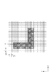
図6は、各サブアレイ(または対物レンズ)あたりの複数のストライプ描画領域SA間の位置関係を説明する図である。対物レンズアレイ9は、対物レンズをX方向に144μmピッチで一次元に配列し、ストライプ描画領域SAが隣接するように、次の行の対物レンズはX方向に2μmだけずらして構成する。同図では、説明をしやすくするため、4行8列の対物レンズアレイを示しているが、実際には、例えば、72行180列の対物レンズアレイとすることができる(総計12960本の対物レンズを含む)。このような構成によれば、ステージ11をY方向に沿った一方向に連続移動(走査)させることにより、ウエハ10上の露光領域EAに描画を行うことができる。
FIG. 6 is a diagram for explaining the positional relationship between a plurality of stripe drawing areas SA for each subarray (or objective lens). The
図7は、1Dレイアウトにおけるカットパターンの描画方法を説明する図である。カットパターンの描画では、図中の「描画パターン」に示すように、所定間隔(例えば同一間隔)でY方向に配列された、X方向の直線上に延びる線状パターンLPが予め形成されている。具体的には、Y方向に50nmピッチで並ぶY方向幅25nmのラインパターンLPが形成されている。その線状パターンLPに対して、線状パターンLPを切断するためのカットパターンCPを描画する。そのため、カットパターンCPのY方向の寸法は、X方向の寸法に比べて大きくすることが必要で、Y方向の寸法精度は、X方向のそれに比べて低くすることができる。更に、カットパターンCPのY方向の描画位置精度も、X方向のそれに比べて低くすることが出来る。 FIG. 7 is a diagram illustrating a drawing method of a cut pattern in the 1D layout. In drawing a cut pattern, as shown in “drawing pattern” in the figure, linear patterns LP arranged in a straight line in the X direction and arranged in a Y direction at a predetermined interval (for example, the same interval) are formed in advance. . Specifically, a line pattern LP having a width of 25 nm in the Y direction arranged at a pitch of 50 nm in the Y direction is formed. A cut pattern CP for cutting the linear pattern LP is drawn on the linear pattern LP. Therefore, the dimension of the cut pattern CP in the Y direction needs to be larger than the dimension in the X direction, and the dimensional accuracy in the Y direction can be made lower than that in the X direction. Furthermore, the drawing position accuracy of the cut pattern CP in the Y direction can be made lower than that in the X direction.
そこで、図中の「パターン開口形状」に示すように、パターン開口アレイのパターン開口は、ウエハ上換算で、横幅PX=30nm、縦幅PY=50nmの矩形としている。ウエハ上のパターン開口の像は、図中の「電子ビーム強度分布」に示すように、Y方向の寸法は、X方向の寸法に比べて大きくなる。 Therefore, as shown in “Pattern opening shape” in the figure, the pattern openings of the pattern opening array are rectangular on the wafer in terms of a horizontal width PX = 30 nm and a vertical width PY = 50 nm. In the image of the pattern opening on the wafer, the dimension in the Y direction is larger than the dimension in the X direction, as indicated by “electron beam intensity distribution” in the figure.
上述のように、カットパターンCPのY方向の描画位置精度は、X方向のそれに比べて低くすることができるため、走査グリッドは、GX=2.5nm、GY=5.0nmのピッチとしている。すなわち、カットパターンCPのX方向(第1方向)の大きさとY方向(第2方向)の大きさとの大小関係と、走査グリッドのピッチGX(第1間隔)とピッチGX(第2間隔)との大小関係とを同じにしている。その描画結果は、図中の「レジスト像」として同図に示すとおりである。分離すべきパターンは、カットパターンにより充分に分離し、その後の工程に問題のないレベルの描画がなされていることがわかる。 As described above, since the drawing position accuracy in the Y direction of the cut pattern CP can be made lower than that in the X direction, the scanning grid has a pitch of GX = 2.5 nm and GY = 5.0 nm. That is, the magnitude relationship between the size of the cut pattern CP in the X direction (first direction) and the size in the Y direction (second direction), the pitch GX (first interval) and the pitch GX (second interval) of the scanning grid. The same size relationship. The drawing result is as shown in the figure as a “resist image” in the figure. It can be seen that the pattern to be separated is sufficiently separated by the cut pattern, and drawing is performed at a level where there is no problem in the subsequent processes.
本実施形態では、描画装置のX−Y軸とウエハ(ウエハに描画されているパターン)の配向とを一致(整合)させる必要がある。そのため、ウエハ10をステージ11に搬送する搬送機構12によって、当該一致(整合)がなされるように、ウエハ10がステージ11に受け渡される。なお、主制御系16等の制御手段は、描画装置のX方向(第1方向)またはY方向(第2方向)とウエハ10の配向とが整合してステージ11にウエハ10が保持されるように、搬送機構12の動作およびステージ11の動作の少なくとも一方を制御すればよい。
In this embodiment, it is necessary to match (align) the XY axes of the drawing apparatus with the orientation of the wafer (pattern drawn on the wafer). Therefore, the
また、グリッドピッチがGX=2.5nm・GY=5.0nmであり、カットパターンCPがPX=30nm・PY=50nmの矩形であるため、当該パターンの情報は、当該グリッドピッチのグリッド点を単位として生成することができる。そのため、パターン情報のハンドリングが容易になり、また、当該パターン情報をグリッド点単位の描画情報に変換する処理の負荷も少ない。 Further, since the grid pitch is GX = 2.5 nm · GY = 5.0 nm and the cut pattern CP is a rectangle of PX = 30 nm · PY = 50 nm, the information of the pattern is in units of grid points of the grid pitch. Can be generated as Therefore, handling of pattern information becomes easy, and the processing load for converting the pattern information into drawing information in units of grid points is small.
図8は、1Dレイアウトにおけるカットパターン描画用の本実施形態に係る描画装置と従来の描画装置との比較を示す図(表)である。当該比較の前提条件は、以下のとおりである。
1)22nm世代に対応する描画装置であること。
2)レジスト感度:20μC/cm2。
3)生産能力:300mmウエハを1時間当たり20枚描画できること。
4)対物レンズ数は、12960本であること。
FIG. 8 is a diagram (table) showing a comparison between the drawing apparatus according to the present embodiment for drawing a cut pattern in a 1D layout and a conventional drawing apparatus. The preconditions for the comparison are as follows.
1) A drawing apparatus corresponding to the 22 nm generation.
2) Resist sensitivity: 20 μC / cm 2 .
3) Production capacity: 20 300 mm wafers can be drawn per hour.
4) The number of objective lenses is 12,960.
従来の描画装置は、どのようなパターンにも対応するため、パターン開口アレイの開口サイズ(PX、PY)も、走査グリッドピッチ(GX、GY)も、X方向とY方向とで同じにしている。その結果、サブアレイの電子ビーム数は、36本で、総電子ビーム数は、466560本である。また、電子源に必要な輝度は、2.3×10⁵(A/sr/cm2)となり、このような輝度では、ディスペンサーカソードのカソード温度が高く、その寿命は短い。また、通信用光ファイバーに必要な伝送速度は、6.38(GBPS)である。この速度に比例して、トランスファーインピーダンスアンプ62・リミッティングアンプ63・シフトレジスタ64の発熱が大きくなるため、従来の描画装置は、ブランカーアレイ6の動作の信頼性の点で不利である。
Since the conventional drawing apparatus supports any pattern, the aperture size (PX, PY) of the pattern aperture array and the scanning grid pitch (GX, GY) are the same in the X direction and the Y direction. . As a result, the number of electron beams in the subarray is 36, and the total number of electron beams is 466560. Further, the luminance required for the electron source is 2.3 × 10 5 (A / sr / cm 2 ), and at such luminance, the cathode temperature of the dispenser cathode is high and its lifetime is short. The transmission rate required for the communication optical fiber is 6.38 (GBPS). Since the heat generation of the
本実施形態の描画装置は、サブアレイの電子ビーム数が16本の場合、従来の描画装置と同様の生産能力を達成するのに、約2分の1の総電子ビーム数のため、約2分の1の伝送速度で済み、しかも電子源に必要な輝度も低くなる。総電子ビーム数が同じ場合は、約2分の1の伝送速度で、2分の1以下の電子源の輝度で、同様の生産能力を達成できる。
以上説明したように、本実施形態によれば、1Dレイアウトのカットパターンを描画する信頼性およびスループットの点で有利な描画装置を提供することができる。
In the drawing apparatus of this embodiment, when the number of electron beams in the subarray is 16, to achieve the same production capacity as that of the conventional drawing apparatus, the total number of electron beams is about 1/2. The transmission speed of 1 is sufficient, and the luminance required for the electron source is also reduced. If the total number of electron beams is the same, a similar production capacity can be achieved with a transmission rate of about one-half and a luminance of the electron source of one-half or less.
As described above, according to this embodiment, it is possible to provide a drawing apparatus that is advantageous in terms of reliability and throughput for drawing a cut pattern of a 1D layout.
[実施形態2]
本実施形態は、1Dレイアウトにおける断続的線状パターンを描画する描画装置に関する。本実施形態は、パターン開口および走査グリッドが異なる他は、実施形態1の構成と同様の構成を有している。
[Embodiment 2]
The present embodiment relates to a drawing apparatus that draws an intermittent linear pattern in a 1D layout. This embodiment has the same configuration as that of the first embodiment except that the pattern opening and the scanning grid are different.
図9は、1Dレイアウトにおける断続的線状パターンの描画方法を説明する図である。本実施形態は、図中の「描画パターン」に示すように、所定間隔(例えば同一間隔)でY方向に配列された、X方向の直線上に延びる断続的線状パターンCLPを描画する。Y方向において、その線状パターンのピッチは50nmで、その線幅は25nmである。この断続的線状パターンCLPにおいては、Y方向の線幅の一様性が重要であり、X方向における線状パターンの端部の形状はあまり重要でない。そのため、断続的線状パターンCLPのY方向の寸法精度は、X方向の寸法精度に比べて高める必要がある。更に、断続的線状パターンCLPのY方向の描画位置精度は、X方向のそれに比べて高める必要がある。 FIG. 9 is a diagram illustrating a method for drawing an intermittent linear pattern in the 1D layout. In the present embodiment, as shown in “drawing pattern” in the drawing, intermittent linear patterns CLP arranged on a straight line in the X direction and arranged in the Y direction at a predetermined interval (for example, the same interval) are drawn. In the Y direction, the pitch of the linear pattern is 50 nm, and the line width is 25 nm. In this intermittent linear pattern CLP, the uniformity of the line width in the Y direction is important, and the shape of the end of the linear pattern in the X direction is not very important. Therefore, the dimensional accuracy in the Y direction of the intermittent linear pattern CLP needs to be higher than the dimensional accuracy in the X direction. Further, the drawing position accuracy in the Y direction of the intermittent linear pattern CLP needs to be higher than that in the X direction.
そこで、図中の「パターン開口形状」に示すように、パターン開口アレイのパターン開口は、ウエハ上換算で、横幅PX=30nm、縦幅PY=25nm の矩形としている。ウエハ上のパターン開口の像は、図中の「電子ビーム強度分布」に示すように、Y方向の寸法は、X方向の寸法に比べて小さくしている。これにより、断続的線状パターンCLPのY方向の寸法精度は、X方向の寸法精度に比べて高めている。 Therefore, as shown in the “pattern opening shape” in the figure, the pattern openings of the pattern opening array are rectangular on the wafer in terms of a horizontal width PX = 30 nm and a vertical width PY = 25 nm. In the image of the pattern opening on the wafer, as shown in the “electron beam intensity distribution” in the figure, the dimension in the Y direction is smaller than the dimension in the X direction. Thereby, the dimensional accuracy in the Y direction of the intermittent linear pattern CLP is higher than the dimensional accuracy in the X direction.
断続的線状パターンCLPのY方向の描画位置精度は、X方向のそれに比べて高くする必要があるため、走査グリッドは、GX=5.0nm、GY=2.5nmのピッチとしている。すなわち、断続的線状パターンCPのX方向(第1方向)の大きさとY方向(第2方向)の大きさとの大小関係と、走査グリッドのピッチGX(第1間隔)とピッチGX(第2間隔)との大小関係とを同じにしている。その描画結果は、「レジスト像」として同図に示すとおりである。断続的線状パターンは、Y方向の線幅が一様となり、その後の工程に問題のないレベルの描画がなされていることがわかる。 Since the drawing position accuracy in the Y direction of the intermittent linear pattern CLP needs to be higher than that in the X direction, the scanning grid has a pitch of GX = 5.0 nm and GY = 2.5 nm. That is, the magnitude relationship between the size of the intermittent linear pattern CP in the X direction (first direction) and the size in the Y direction (second direction), the pitch GX (first interval) and the pitch GX (second) of the scanning grid. The size relationship with the interval is the same. The drawing result is as shown in the figure as a “resist image”. It can be seen that the intermittent linear pattern has a uniform line width in the Y direction and is drawn at a level with no problem in the subsequent processes.
本実施形態も、実施形態1と同様に、描画装置のX−Y軸とウエハ(ウエハに描画されているパターン)の配向とを一致(整合)させる必要がある。そのため、ウエハ10をステージ11に搬送する搬送機構12によって、当該一致(整合)がなされるように、ウエハ10がステージ11に受け渡される。なお、主制御系16等の制御手段は、描画装置のX方向(第1方向)またはY方向(第2方向)とウエハ10の配向とが整合してステージ11にウエハ10が保持されるように、搬送機構12の動作およびステージ11の動作の少なくとも一方を制御すればよい。
In the present embodiment, as in the first embodiment, it is necessary to match (align) the XY axes of the drawing apparatus and the orientation of the wafer (pattern drawn on the wafer). Therefore, the
図8を再度参照して、1Dレイアウトにおける断続的線状パターンを描画する本実施形態に係る描画装置と従来の描画装置との比較を行う。当該比較の前提条件は、先述したとおりである。
従来の描画装置では、どのようなパターンにも対応するため、パターン開口アレイのパターン開口のサイズ(PX、PY)も、走査グリッドのピッチ(GX、GY)も、X方向とY方向とで同じにしている。その結果、サブアレイの電子ビーム数は、49本で、総電子ビーム数は635040本である。また、電子源に必要な輝度は、2.3×10⁵(A/sr/cm2)となり、このような輝度では、ディスペンサーカソードのカソード温度が高く、寿命は短い。また、通信用光ファイバーに必要な伝送速度は、6.38(GBPS)である。この速度に比例して、トランスファーインピーダンスアンプ62・リミッティングアンプ63・シフトレジスタ64の発熱が大きくななるため、従来の描画装置は、ブランカーアレイ6の動作の信頼性の点で不利である。
Referring to FIG. 8 again, the drawing apparatus according to the present embodiment that draws the intermittent linear pattern in the 1D layout is compared with the conventional drawing apparatus. The preconditions for the comparison are as described above.
Since the conventional drawing apparatus supports any pattern, the pattern opening size (PX, PY) and the scanning grid pitch (GX, GY) of the pattern opening array are the same in the X direction and the Y direction. I have to. As a result, the number of electron beams in the subarray is 49, and the total number of electron beams is 635,040. In addition, the luminance required for the electron source is 2.3 × 10 5 (A / sr / cm 2 ). At such luminance, the cathode temperature of the dispenser cathode is high and the lifetime is short. The transmission rate required for the communication optical fiber is 6.38 (GBPS). Since the heat generation of the
本実施形態の描画装置は、総電子ビーム数は同じであるが、約2分の1の伝送速度で、かつ、より少ない電子源の輝度で、従来の描画装置と同様の生産能力を達成できる。
以上説明したように、本実施形態によれば、1Dレイアウトの断続的線状パターンを描画する信頼性およびスループットの点で有利な描画装置を提供することができる。
The drawing apparatus of the present embodiment has the same total number of electron beams, but can achieve the same production capacity as a conventional drawing apparatus with a transmission speed of about one-half and with a lower brightness of the electron source. .
As described above, according to the present embodiment, it is possible to provide a drawing apparatus that is advantageous in terms of reliability and throughput for drawing an intermittent linear pattern of a 1D layout.
[実施形態3]
本発明の実施形態に係る物品の製造方法は、例えば、半導体デバイス等のマイクロデバイスや微細構造を有する素子等の物品を製造するのに好適である。該製造方法は、感光剤が塗布された基板の該感光剤に上記の描画装置を用いて潜像パターンを形成する工程(基板に描画を行う工程)と、当該工程で潜像パターンが形成された基板を現像する工程とを含みうる。さらに、該製造方法は、他の周知の工程(酸化、成膜、蒸着、ドーピング、平坦化、エッチング、レジスト剥離、ダイシング、ボンディング、パッケージング等)を含みうる。本実施形態の物品の製造方法は、従来の方法に比べて、物品の性能・品質・生産性・生産コストの少なくとも1つにおいて有利である。
[Embodiment 3]
The method for manufacturing an article according to an embodiment of the present invention is suitable for manufacturing an article such as a microdevice such as a semiconductor device or an element having a fine structure. The manufacturing method includes a step of forming a latent image pattern on the photosensitive agent on the substrate coated with the photosensitive agent using the above drawing apparatus (a step of drawing on the substrate), and the latent image pattern is formed in the step. Developing the substrate. Further, the manufacturing method may include other well-known steps (oxidation, film formation, vapor deposition, doping, planarization, etching, resist stripping, dicing, bonding, packaging, and the like). The method for manufacturing an article according to the present embodiment is advantageous in at least one of the performance, quality, productivity, and production cost of the article as compared with the conventional method.
以上、本発明の実施形態について説明したが、本発明はこれらの実施形態に限定されず、その要旨の範囲内で種々の変形および変更が可能である。 As mentioned above, although embodiment of this invention was described, this invention is not limited to these embodiment, A various deformation | transformation and change are possible within the range of the summary.
1 電子源
2 コリメータレンズ
3 アパーチャアレイ
4 コンデンサーレンズアレイ
5 パターン開口アレイ
6 ブランカーアレイ
7 ブランキングアパーチャアレイ
8 偏向器アレイ
9 対物レンズアレイ
11 ステージ
13 ブランキング制御回路
14 偏向器制御回路
15 ステージ制御回路
16 主制御系
DESCRIPTION OF
Claims (11)
前記複数の荷電粒子線それぞれの前記基板上でのサイズを規定する開口を有するアパーチャアレイ部材と、
前記複数の荷電粒子線を個別にブランキングするブランカアレイと、
互いに交差する第1方向および第2方向それぞれにおいて前記複数の荷電粒子線と前記基板との間の相対走査を行うことにより前記複数の荷電粒子線と前記基板との間のラスター走査を行う走査手段と、
前記ラスター走査に並行して、前記基板上において、前記第1方向および前記第2方向のうちの少なくとも一つに関して、前記複数の荷電粒子線のピッチより小さい所定ピッチをもって前記ブランカアレイによるブランキングを制御する制御手段と、を有し、
前記サイズおよび前記所定ピッチは、前記第1方向および前記第2方向のうちの前記少なくとも一つのうちの一つにおいてより前記第1方向および前記第2方向のうちの他の一つにおいての方が小さい、ことを特徴とする描画装置。 A drawing apparatus for drawing on a substrate with a plurality of charged particle beams,
An aperture array member having an opening for defining a size of each of the plurality of charged particle beams on the substrate;
A blanker array for individually blanking the plurality of charged particle beams;
Scanning means for performing raster scanning between the plurality of charged particle beams and the substrate by performing relative scanning between the plurality of charged particle beams and the substrate in each of a first direction and a second direction intersecting each other. When,
Wherein in parallel to the raster scan, in the substrate, for at least one of said first and second directions, blanking by the blanker array with a smaller predetermined pitch than the pitch of the plurality of charged particle beams Control means for controlling ranking , and
The size and the predetermined pitch, the direction of the other one of said first direction and said more the first direction and the second direction in one one of the at least one of the second direction A drawing apparatus characterized by being small.
前記制御手段は、前記サイズおよび前記所定ピッチがより大きい前記第1方向および前記第2方向のうちの一つが前記基板に描画されるべきパターンの長手方向に整合して前記ステージに前記基板が保持されるように、前記搬送機構の動作および前記ステージの動作のうちの少なくとも一方を制御する、ことを特徴とする請求項1ないし請求項3のうちいずれか1項に記載の描画装置。 A stage for holding the substrate; and a transport mechanism for transporting the substrate to the stage;
The control means is configured to align the substrate on the stage so that one of the first direction and the second direction having a larger size and the predetermined pitch is aligned with a longitudinal direction of a pattern to be drawn on the substrate. as will be retained, the drawing apparatus according to any one of claims 1 to 3 wherein the controlling at least one of the operations of the operation and the stage of the transport mechanism, characterized in that.
前記複数の荷電粒子線それぞれの前記基板上でのサイズを規定する開口を有するアパーチャアレイ部材と、
前記複数の荷電粒子線のそれぞれを前記基板に入射させるか否かを切り替える切替手段と、
互いに交差する第1方向および第2方向それぞれにおいて前記複数の荷電粒子線と前記基板との間の相対走査を行うことにより前記複数の荷電粒子線と前記基板との間のラスター走査を行う走査手段と、
前記ラスター走査に並行して、前記基板上において、前記第1方向および前記第2方向のうちの少なくとも一つに関して、前記複数の荷電粒子線のピッチより小さい所定ピッチをもって前記切替手段による切り替えを制御する制御手段と、を有し、
前記サイズおよび前記所定ピッチは、前記第1方向および前記第2方向のうちの前記少なくとも一つのうちの一つにおいてより前記第1方向および前記第2方向のうちの他の一つにおいての方が小さい、ことを特徴とする描画装置。 A drawing apparatus for drawing on a substrate with a plurality of charged particle beams,
An aperture array member having an opening for defining a size of each of the plurality of charged particle beams on the substrate;
Switching means for switching whether or not each of the plurality of charged particle beams is incident on the substrate;
Scanning means for performing raster scanning between the plurality of charged particle beams and the substrate by performing relative scanning between the plurality of charged particle beams and the substrate in each of a first direction and a second direction intersecting each other. When,
In parallel with the raster scanning, switching by the switching unit is performed on the substrate with a predetermined pitch smaller than the pitch of the plurality of charged particle beams in at least one of the first direction and the second direction. Control means for controlling
The size and the predetermined pitch, the direction of the other one of said first direction and said more the first direction and the second direction in one one of the at least one of the second direction A drawing apparatus characterized by being small.
前記複数の荷電粒子線それぞれを、前記基板上でのサイズを規定して、前記基板上に投影し、
互いに交差する第1方向および第2方向それぞれにおいて前記複数の荷電粒子線と前記基板との間の相対走査を行うことにより前記複数の荷電粒子線と前記基板との間のラスター走査を行い、
前記ラスター走査に並行して、前記基板上において、前記第1方向および前記第2方向のうちの少なくとも一つに関して、前記複数の荷電粒子線のピッチより小さい所定ピッチをもって前記複数の荷電粒子線を個別にブランキングし、
前記サイズおよび前記所定ピッチは、前記第1方向および前記第2方向のうちの前記少なくとも一つのうちの一つにおいてより前記第1方向および前記第2方向のうちの他の一つにおいての方が小さい、ことを特徴とする描画方法。 A drawing method for drawing on a substrate with a plurality of charged particle beams,
Each of the plurality of charged particle beams is defined on the substrate and projected onto the substrate;
Performing a raster scan between the plurality of charged particle beams and the substrate by performing a relative scan between the plurality of charged particle beams and the substrate in each of a first direction and a second direction intersecting each other;
In parallel with the raster scanning, the plurality of charged particles have a predetermined pitch smaller than the pitch of the plurality of charged particle beams with respect to at least one of the first direction and the second direction on the substrate. Blank lines individually,
The size and the predetermined pitch, the direction of the other one of said first direction and said more the first direction and the second direction in one one of the at least one of the second direction A drawing method characterized by being small.
前記複数の荷電粒子線それぞれを、前記基板上でのサイズを規定して、前記基板上に投影し、
互いに交差する第1方向および第2方向それぞれにおいて前記複数の荷電粒子線と前記基板との間の相対走査を行うことにより前記複数の荷電粒子線と前記基板との間のラスター走査を行い、
前記ラスター走査に並行して、前記基板上において、前記第1方向および前記第2方向のうちの少なくとも一つに関して、前記複数の荷電粒子線のピッチより小さい所定ピッチをもって前記複数の荷電粒子線のそれぞれを前記基板に入射させるか否かを切り替え、
前記サイズおよび前記所定ピッチは、前記第1方向および前記第2方向のうちの前記少なくとも一つのうちの一つにおいてより前記第1方向および前記第2方向のうちの他の一つにおいての方が小さい、ことを特徴とする描画方法。 A drawing method for drawing on a substrate with a plurality of charged particle beams,
Each of the plurality of charged particle beams is defined on the substrate and projected onto the substrate;
Performing a raster scan between the plurality of charged particle beams and the substrate by performing a relative scan between the plurality of charged particle beams and the substrate in each of a first direction and a second direction intersecting each other;
In parallel with the raster scanning, the plurality of charged particles have a predetermined pitch smaller than the pitch of the plurality of charged particle beams with respect to at least one of the first direction and the second direction on the substrate. Switching whether each of the lines is incident on the substrate ,
The size and the predetermined pitch, the direction of the other one of said first direction and said more the first direction and the second direction in one one of the at least one of the second direction A drawing method characterized by being small.
Priority Applications (2)
| Application Number | Priority Date | Filing Date | Title |
|---|---|---|---|
| JP2011040270A JP5744564B2 (en) | 2011-02-25 | 2011-02-25 | Drawing apparatus, drawing method, and article manufacturing method |
| US13/402,071 US20120219914A1 (en) | 2011-02-25 | 2012-02-22 | Drawing apparatus, drawing method and method of manufacturing article |
Applications Claiming Priority (1)
| Application Number | Priority Date | Filing Date | Title |
|---|---|---|---|
| JP2011040270A JP5744564B2 (en) | 2011-02-25 | 2011-02-25 | Drawing apparatus, drawing method, and article manufacturing method |
Publications (3)
| Publication Number | Publication Date |
|---|---|
| JP2012178437A JP2012178437A (en) | 2012-09-13 |
| JP2012178437A5 JP2012178437A5 (en) | 2014-04-10 |
| JP5744564B2 true JP5744564B2 (en) | 2015-07-08 |
Family
ID=46719210
Family Applications (1)
| Application Number | Title | Priority Date | Filing Date |
|---|---|---|---|
| JP2011040270A Expired - Fee Related JP5744564B2 (en) | 2011-02-25 | 2011-02-25 | Drawing apparatus, drawing method, and article manufacturing method |
Country Status (2)
| Country | Link |
|---|---|
| US (1) | US20120219914A1 (en) |
| JP (1) | JP5744564B2 (en) |
Families Citing this family (20)
| Publication number | Priority date | Publication date | Assignee | Title |
|---|---|---|---|---|
| JP5826566B2 (en) * | 2011-09-01 | 2015-12-02 | 株式会社ニューフレアテクノロジー | Multi-charged particle beam writing apparatus and multi-charged particle beam writing method |
| JP6087506B2 (en) * | 2012-01-31 | 2017-03-01 | キヤノン株式会社 | Drawing method and article manufacturing method |
| JP6087570B2 (en) * | 2012-10-15 | 2017-03-01 | キヤノン株式会社 | Drawing apparatus and article manufacturing method |
| JP6195349B2 (en) * | 2013-04-26 | 2017-09-13 | キヤノン株式会社 | Drawing apparatus, drawing method, and article manufacturing method |
| JP2014229694A (en) * | 2013-05-21 | 2014-12-08 | 株式会社東芝 | Semiconductor device and manufacturing method of the same |
| JP6418786B2 (en) * | 2013-07-10 | 2018-11-07 | キヤノン株式会社 | Pattern creating method, program, and information processing apparatus |
| JP6215061B2 (en) * | 2014-01-14 | 2017-10-18 | 株式会社アドバンテスト | Electron beam exposure system |
| JP6211435B2 (en) * | 2014-02-26 | 2017-10-11 | 株式会社アドバンテスト | Manufacturing method of semiconductor device |
| EP2937888B1 (en) * | 2014-04-25 | 2019-02-20 | IMS Nanofabrication GmbH | Multi-beam tool for cutting patterns |
| US10014256B2 (en) | 2014-06-13 | 2018-07-03 | Intel Corporation | Unidirectional metal on layer with ebeam |
| US10386722B2 (en) | 2014-06-13 | 2019-08-20 | Intel Corporation | Ebeam staggered beam aperture array |
| US10216087B2 (en) | 2014-06-13 | 2019-02-26 | Intel Corporation | Ebeam universal cutter |
| KR102373197B1 (en) * | 2014-06-13 | 2022-03-11 | 인텔 코포레이션 | Ebeam non-universal cutter |
| US9897908B2 (en) | 2014-06-13 | 2018-02-20 | Intel Corporation | Ebeam three beam aperture array |
| US20170069509A1 (en) * | 2014-06-13 | 2017-03-09 | Intel Corporation | Data compression for ebeam throughput |
| CN106716597B (en) * | 2014-08-19 | 2021-02-23 | 英特尔公司 | Filleting correction for Electron Beam (EBEAM) direct write systems |
| WO2016028334A1 (en) | 2014-08-19 | 2016-02-25 | Intel Corporation | Cross scan proximity correction with ebeam universal cutter |
| JP6484431B2 (en) * | 2014-11-12 | 2019-03-13 | 株式会社アドバンテスト | Charged particle beam exposure apparatus and charged particle beam exposure method |
| WO2018155538A1 (en) * | 2017-02-24 | 2018-08-30 | 株式会社ニコン | Electron beam apparatus and exposure method, and device production method |
| WO2018167936A1 (en) * | 2017-03-17 | 2018-09-20 | 株式会社ニコン | Exposure device, lithographic method, and device manufacturing method |
Family Cites Families (5)
| Publication number | Priority date | Publication date | Assignee | Title |
|---|---|---|---|---|
| JPH10284377A (en) * | 1997-04-07 | 1998-10-23 | Nikon Corp | Exposure method and manufacture of device using the same |
| US6014200A (en) * | 1998-02-24 | 2000-01-11 | Nikon Corporation | High throughput electron beam lithography system |
| US7465973B2 (en) * | 2004-12-03 | 2008-12-16 | International Business Machines Corporation | Integrated circuit having gates and active regions forming a regular grating |
| US8198655B1 (en) * | 2009-04-27 | 2012-06-12 | Carnegie Mellon University | Regular pattern arrays for memory and logic on a semiconductor substrate |
| JP5988537B2 (en) * | 2010-06-10 | 2016-09-07 | 株式会社ニコン | Charged particle beam exposure apparatus and device manufacturing method |
-
2011
- 2011-02-25 JP JP2011040270A patent/JP5744564B2/en not_active Expired - Fee Related
-
2012
- 2012-02-22 US US13/402,071 patent/US20120219914A1/en not_active Abandoned
Also Published As
| Publication number | Publication date |
|---|---|
| JP2012178437A (en) | 2012-09-13 |
| US20120219914A1 (en) | 2012-08-30 |
Similar Documents
| Publication | Publication Date | Title |
|---|---|---|
| JP5744564B2 (en) | Drawing apparatus, drawing method, and article manufacturing method | |
| JP6087506B2 (en) | Drawing method and article manufacturing method | |
| US6870172B1 (en) | Maskless reflection electron beam projection lithography | |
| US6903353B2 (en) | Charged particle beam exposure apparatus, device manufacturing method, and charged particle beam applied apparatus | |
| JP3787417B2 (en) | Electron beam exposure method and electron beam exposure apparatus | |
| US7755061B2 (en) | Dynamic pattern generator with cup-shaped structure | |
| US8026495B2 (en) | Charged particle beam exposure system | |
| JP2005129944A (en) | Charged-particle multibeam exposure device | |
| NL2010795A (en) | Method for determining a beamlet position and method for determining a distance between two beamlets in a multi-beamlet exposure apparatus. | |
| JP6128744B2 (en) | Drawing apparatus, drawing method, and article manufacturing method | |
| US8089051B2 (en) | Electron reflector with multiple reflective modes | |
| KR20220123701A (en) | charged particle manipulator | |
| US20140106279A1 (en) | Drawing apparatus, and method of manufacturing article | |
| US7173262B2 (en) | Charged particle beam exposure apparatus, charged particle beam exposure method and device manufacturing method | |
| JPH1187206A (en) | Electron beam aligner and manufacture of device using the same | |
| US8253119B1 (en) | Well-based dynamic pattern generator | |
| US9001387B2 (en) | Drawing apparatus, data processing method, and method of manufacturing article that transform partially overlapping regions using different transformation rules | |
| KR20140130028A (en) | Drawing apparatus, and method of manufacturing article | |
| US7049610B2 (en) | Charged particle beam exposure method, charged particle beam exposure apparatus, and device manufacturing method | |
| US9040942B1 (en) | Electron beam lithography with linear column array and rotary stage | |
| JP4477433B2 (en) | Electron beam exposure apparatus and multi-beam electron optical system | |
| US20140162191A1 (en) | Drawing apparatus, and method of manufacturing article | |
| JP4006054B2 (en) | Electron beam exposure system | |
| JPH10199469A (en) | Electron beam lighting device and electron beam aligner with the lighting device | |
| JP2004153294A (en) | Electron beam exposure device, electron beam exposure method and device manufacturing method |
Legal Events
| Date | Code | Title | Description |
|---|---|---|---|
| A521 | Request for written amendment filed |
Free format text: JAPANESE INTERMEDIATE CODE: A523 Effective date: 20140225 |
|
| A621 | Written request for application examination |
Free format text: JAPANESE INTERMEDIATE CODE: A621 Effective date: 20140225 |
|
| A977 | Report on retrieval |
Free format text: JAPANESE INTERMEDIATE CODE: A971007 Effective date: 20141127 |
|
| A131 | Notification of reasons for refusal |
Free format text: JAPANESE INTERMEDIATE CODE: A131 Effective date: 20141202 |
|
| A521 | Request for written amendment filed |
Free format text: JAPANESE INTERMEDIATE CODE: A523 Effective date: 20150202 |
|
| TRDD | Decision of grant or rejection written | ||
| A01 | Written decision to grant a patent or to grant a registration (utility model) |
Free format text: JAPANESE INTERMEDIATE CODE: A01 Effective date: 20150407 |
|
| A61 | First payment of annual fees (during grant procedure) |
Free format text: JAPANESE INTERMEDIATE CODE: A61 Effective date: 20150430 |
|
| LAPS | Cancellation because of no payment of annual fees |