JP4477436B2 - Charged particle beam exposure system - Google Patents
Charged particle beam exposure system Download PDFInfo
- Publication number
- JP4477436B2 JP4477436B2 JP2004194775A JP2004194775A JP4477436B2 JP 4477436 B2 JP4477436 B2 JP 4477436B2 JP 2004194775 A JP2004194775 A JP 2004194775A JP 2004194775 A JP2004194775 A JP 2004194775A JP 4477436 B2 JP4477436 B2 JP 4477436B2
- Authority
- JP
- Japan
- Prior art keywords
- blanking
- charged particle
- electron beam
- particle beam
- electron
- Prior art date
- Legal status (The legal status is an assumption and is not a legal conclusion. Google has not performed a legal analysis and makes no representation as to the accuracy of the status listed.)
- Expired - Fee Related
Links
Images


Classifications
-
- H—ELECTRICITY
- H01—ELECTRIC ELEMENTS
- H01J—ELECTRIC DISCHARGE TUBES OR DISCHARGE LAMPS
- H01J37/00—Discharge tubes with provision for introducing objects or material to be exposed to the discharge, e.g. for the purpose of examination or processing thereof
- H01J37/02—Details
- H01J37/04—Arrangements of electrodes and associated parts for generating or controlling the discharge, e.g. electron-optical arrangement, ion-optical arrangement
- H01J37/045—Beam blanking or chopping, i.e. arrangements for momentarily interrupting exposure to the discharge
-
- B—PERFORMING OPERATIONS; TRANSPORTING
- B82—NANOTECHNOLOGY
- B82Y—SPECIFIC USES OR APPLICATIONS OF NANOSTRUCTURES; MEASUREMENT OR ANALYSIS OF NANOSTRUCTURES; MANUFACTURE OR TREATMENT OF NANOSTRUCTURES
- B82Y10/00—Nanotechnology for information processing, storage or transmission, e.g. quantum computing or single electron logic
-
- B—PERFORMING OPERATIONS; TRANSPORTING
- B82—NANOTECHNOLOGY
- B82Y—SPECIFIC USES OR APPLICATIONS OF NANOSTRUCTURES; MEASUREMENT OR ANALYSIS OF NANOSTRUCTURES; MANUFACTURE OR TREATMENT OF NANOSTRUCTURES
- B82Y40/00—Manufacture or treatment of nanostructures
-
- H—ELECTRICITY
- H01—ELECTRIC ELEMENTS
- H01J—ELECTRIC DISCHARGE TUBES OR DISCHARGE LAMPS
- H01J37/00—Discharge tubes with provision for introducing objects or material to be exposed to the discharge, e.g. for the purpose of examination or processing thereof
- H01J37/30—Electron-beam or ion-beam tubes for localised treatment of objects
- H01J37/317—Electron-beam or ion-beam tubes for localised treatment of objects for changing properties of the objects or for applying thin layers thereon, e.g. for ion implantation
- H01J37/3174—Particle-beam lithography, e.g. electron beam lithography
-
- H—ELECTRICITY
- H01—ELECTRIC ELEMENTS
- H01J—ELECTRIC DISCHARGE TUBES OR DISCHARGE LAMPS
- H01J2237/00—Discharge tubes exposing object to beam, e.g. for analysis treatment, etching, imaging
- H01J2237/04—Means for controlling the discharge
- H01J2237/043—Beam blanking
- H01J2237/0435—Multi-aperture
-
- H—ELECTRICITY
- H01—ELECTRIC ELEMENTS
- H01J—ELECTRIC DISCHARGE TUBES OR DISCHARGE LAMPS
- H01J2237/00—Discharge tubes exposing object to beam, e.g. for analysis treatment, etching, imaging
- H01J2237/30—Electron or ion beam tubes for processing objects
- H01J2237/317—Processing objects on a microscale
- H01J2237/3175—Lithography
- H01J2237/31774—Multi-beam
Description
本発明は、電子線やイオンビーム等の荷電粒子線を用いて露光を行う荷電粒子線露光装置および方法に関し、特に、荷電粒子線をブランキングしながら被露光基板に描画する荷電粒子線露光装置および方法に関するものである。このような装置および方法は、主に半導体集積回路等の露光に用いられる。 The present invention relates to a charged particle beam exposure apparatus and method for performing exposure using a charged particle beam such as an electron beam or an ion beam, and more particularly to a charged particle beam exposure apparatus for drawing a charged particle beam on an exposed substrate while blanking the charged particle beam. And methods. Such an apparatus and method are mainly used for exposure of a semiconductor integrated circuit or the like.
従来のラスタースキャン型電子ビーム露光装置を図11に示す。
電子源101から放出された電子ビームは電磁レンズ102によって電子源101の像103を形成する。その電子源像103は電磁レンズ105、108から成る縮小電子光学系を介してウエハ109上に縮小投影される。ブランカー104は電子源像103の位置にある静電型偏向器で、ウエハ109に対する電子ビームの照射と遮蔽を制御する。すなわち、電子ビームをウエハ109に対して照射する場合は、ブランカー104を用いずに、ウエハ109上に電子ビームを照射する。一方、電子ビームをウエハ109に対して遮蔽する場合は、ブランカー104を用いて電子ビームを偏向させ、縮小電子光学系の瞳上に位置するブランキングアパーチャ106で電子ビームを遮蔽する。また、電子ビームは静電偏向器107によってウエハ上を走査される。
A conventional raster scan type electron beam exposure apparatus is shown in FIG.
The electron beam emitted from the
次にラスタースキャンでウエハ109を描画する方法を図12を用いて説明する。例えばパターン「A」を描画したい場合、まず描画領域を複数のピクセル201に分割する。そして、静電偏向器を用いて電子ビーム202をX方向に走査しながら、電子ビーム202の照射と遮蔽を制御することで、描画すべきパターン部分のピクセル203においてのみ電子ビームの照射を行う。X方向の走査が終了すると、電子ビーム202はY方向にステップし、X方向の走査を同様に行うことでパターン「A」全体を描画する。
しかしながら、電子ビームをラスタースキャンしてピクセルを露光する場合、図13(A)に示すように、電子ビームのピクセル内での位置は、ラスタースキャン方向(X方向)では時間とともに変化するが、ラスタースキャン方向と直交する方向(Y方向)では時間とともに変化しない。すなわち、ラスタースキャン方向(X方向)のピクセル内でのビーム電流強度分布は、図13(B)に示すように、電子ビームがピクセル内を移動した時の移動平均となる。図13(C)にその結果であるピクセル内のビーム電流強度分布を示す。したがって、たとえビーム電流強度分布が軸対称なガウス分布であったとしても、ラスタースキャンで描画するとラスタースキャン方向(X方向)にビーム電流強度分布が広がり、あたかもその方向にぼけたかのようになる。そのため、所望のパターン寸法精度を得ることが難しい。 However, when a pixel is exposed by raster scanning with an electron beam, the position of the electron beam within the pixel changes with time in the raster scan direction (X direction) as shown in FIG. It does not change with time in the direction orthogonal to the scan direction (Y direction). That is, the beam current intensity distribution in the pixel in the raster scan direction (X direction) is a moving average when the electron beam moves in the pixel, as shown in FIG. FIG. 13C shows the resulting beam current intensity distribution in the pixel. Therefore, even if the beam current intensity distribution is an axially symmetric Gaussian distribution, when drawing with raster scan, the beam current intensity distribution spreads in the raster scan direction (X direction), as if it were blurred in that direction. Therefore, it is difficult to obtain a desired pattern dimension accuracy.
さらに、電子ビームが電磁レンズや偏向器の影響で非点収差やコマ収差を持っており、ビーム電流強度分布がガウス分布でない場合も、所望のパターン寸法精度を得ることが難しい。この問題は、ラスタースキャン型であるか否かに関わらず、生じる問題である。
本発明は、上述の従来例における問題点を解消することを課題とする。
Furthermore, it is difficult to obtain a desired pattern dimension accuracy even when the electron beam has astigmatism or coma due to the influence of an electromagnetic lens or a deflector and the beam current intensity distribution is not a Gaussian distribution. This problem occurs regardless of whether the raster scan type is used.
An object of the present invention is to solve the problems in the above-described conventional example.
上記課題を解決するための本発明の荷電粒子線露光装置は、荷電粒子線を用いて被露光基板上にパターンを露光する荷電粒子線露光装置であって、前記荷電粒子線を偏向可能な偏向器を有し、前記荷電粒子線を偏向して前記被露光基板への照射を制御するブランキング手段と、前記偏向器による前記荷電粒子線のブランキング方向を調整する調整手段と、前記被露光基板に対して前記荷電粒子線を走査させる走査手段と、を備え、前記ブランキング手段は、前記荷電粒子線を通過させるためのブランキングアパーチャを有し、前記偏向器は、前記ブランキングアパーチャを挟んで異なる4つの方向に配置された4対の電極を含み、前記荷電粒子線を少なくとも4つの方向に偏向可能であり、前記調整手段は、前記荷電粒子線のブランキング方向を前記荷電粒子線の走査方向と垂直な方向に調整することを特徴とする。 A charged particle beam exposure apparatus of the present invention for solving the above-mentioned problems is a charged particle beam exposure apparatus that exposes a pattern on a substrate to be exposed using a charged particle beam, and deflects the deflected charged particle beam. A blanking unit that deflects the charged particle beam to control irradiation to the substrate to be exposed, an adjusting unit that adjusts a blanking direction of the charged particle beam by the deflector, and the exposure target. Scanning means for scanning the charged particle beam with respect to the substrate, the blanking means has a blanking aperture for allowing the charged particle beam to pass through, and the deflector includes the blanking aperture. Including four pairs of electrodes arranged in four different directions, and capable of deflecting the charged particle beam in at least four directions, wherein the adjusting means is configured to blank the charged particle beam. The and adjusting the scanning direction perpendicular to the direction of the charged particle beam.
本発明によれば、パターン寸法精度の良い荷電粒子線露光装置および露光方法を提供することができる。 According to the present invention, it is possible to provide a charged particle beam exposure apparatus and an exposure method with good pattern dimension accuracy .
以下、本発明の実施の形態を実施例を挙げて説明する。
ここでは、荷電粒子線露光装置の例として、(1)ラスタースキャン方向と垂直な方向にブランキングを行う(以下、ブランキングのために電子ビームを偏向する方向をブラン
キング方向という)電子ビーム露光装置、(2)ビーム径が最も短い方向にブランキングを行う電子ビーム露光装置(1本の電子ビームを用いる場合)、(3)ビーム径が最も短い方向にブランキングを行う電子ビーム露光装置(複数の電子ビームを用いる場合)の例を示す。なお、本発明は、電子ビームに限らずイオンビームを用いた露光装置にも同様に適用できる。
Hereinafter, embodiments of the present invention will be described with reference to examples.
Here, as an example of a charged particle beam exposure apparatus, (1) blanking is performed in a direction perpendicular to the raster scan direction (hereinafter, the direction in which the electron beam is deflected for blanking is referred to as the blanking direction). (2) Electron beam exposure apparatus that blanks in the direction with the shortest beam diameter (when using one electron beam), (3) Electron beam exposure apparatus that performs blanking in the direction with the shortest beam diameter ( An example of using a plurality of electron beams is shown. Note that the present invention is not limited to an electron beam and can be similarly applied to an exposure apparatus using an ion beam.
[第1の実施例]
(1)ラスタースキャン方向と垂直な方向にブランキングを行う電子ビーム露光装置 本実施例のラスタースキャン方向と垂直な方向にブランキングを行う電子ビーム露光装置について、ラスタースキャン方向と垂直な方向に電子ビームをブランキングさせることで、描画パターンの寸法精度を向上出来ることを示す。
[First embodiment]
(1) Electron beam exposure apparatus that performs blanking in a direction perpendicular to the raster scan direction The electron beam exposure apparatus that performs blanking in a direction perpendicular to the raster scan direction according to the present embodiment has an electron in a direction perpendicular to the raster scan direction. It shows that the dimensional accuracy of the drawing pattern can be improved by blanking the beam.
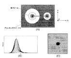
まず、ブランキング方向にビーム電流強度分布が広がることを、図1を用いて示す。 図1(A)に示すように、ブランキング動作は、ブランカーを作動させずブランキングアパーチャを電子ビームが通過している状態から、ブランカーを作動させ電子ビームをX方向に移動してブランキングアパーチャで遮蔽された状態にする動作である。その際、電子ビームは一定の遷移時間をかけてX方向に移動する。その時、ウエハ上のビーム電流強度分布は、図1(B)に示すように、電子ビームがブランキングアパーチャに遮蔽されながら移動する時の移動平均となる。その結果、ブランキング遷移過程でのビーム電流強度分布は図1(C)のようになる。たとえ電子ビームの強度分布が軸対称なガウス分布であったとしても、ブランキング遷移過程でブランキング方向(X方向)にビーム電流強度分布が広がり、あたかもその方向にぼけたかのようになる。 First, it will be shown using FIG. 1 that the beam current intensity distribution spreads in the blanking direction. As shown in FIG. 1A, the blanking operation is performed by operating the blanker and moving the electron beam in the X direction from the state in which the electron beam passes through the blanking aperture without operating the blanker. It is an operation to make it shielded by. At that time, the electron beam moves in the X direction over a certain transition time. At that time, the beam current intensity distribution on the wafer is a moving average when the electron beam moves while being blocked by the blanking aperture, as shown in FIG. As a result, the beam current intensity distribution in the blanking transition process is as shown in FIG. Even if the electron beam intensity distribution is an axially symmetric Gaussian distribution, the beam current intensity distribution spreads in the blanking direction (X direction) in the blanking transition process, as if it were blurred in that direction.
前記したように、ラスタースキャンでラスタースキャン方向に電子ビームはぼけ、ブランキングでもブランキング方向に電子ビームはぼける。よって、ラスタースキャン方向と垂直な方向に電子ビームをブランキングさせることで、電子ビームのラスタースキャン方向のぼけを相殺することができ、描画パターンの寸法精度を向上させることが出来る。 As described above, the electron beam is blurred in the raster scan direction by the raster scan, and the electron beam is blurred in the blanking direction by the blanking. Therefore, by blanking the electron beam in a direction perpendicular to the raster scan direction, blurring of the electron beam in the raster scan direction can be canceled, and the dimensional accuracy of the drawing pattern can be improved.
図2(A)に、ラスタースキャン方向とブランキング方向を一致させた場合のパターン寸法精度のグラフを、図2(B)に、ラスタースキャン方向とブランキング方向を垂直にした場合のパターン寸法精度のグラフを、それぞれ示す。図2(A)、(B)は計算から求めたグラフである。横軸はフォーカスのずれ量、縦軸はパターン寸法精度である。+2ミクロンのフォーカスのずれがある場合、パターン寸法精度が3倍以上向上していることが分かる。 つまり、ブランキング手段を用いて基板を露光する電子ビーム露光装置において、ブランキングの方向をあらかじめ決められた方向に調整する機能を有することで、パターン寸法精度を向上することが出来る。 FIG. 2A shows a graph of pattern dimensional accuracy when the raster scan direction and the blanking direction are matched, and FIG. 2B shows pattern dimensional accuracy when the raster scan direction and the blanking direction are perpendicular. These graphs are shown respectively. 2A and 2B are graphs obtained from calculation. The horizontal axis represents the focus shift amount, and the vertical axis represents the pattern dimension accuracy. It can be seen that when the focus shift is +2 microns, the pattern dimensional accuracy is improved by 3 times or more. In other words, the electron beam exposure apparatus that exposes the substrate using the blanking means has a function of adjusting the blanking direction to a predetermined direction, thereby improving the pattern dimension accuracy.
[第2の実施例]
(2)ビーム径が最も短い方向にブランキングを行う電子ビーム露光装置
(1本の電子ビームを用いる場合)
図3を用いて本実施例の電子ビーム露光装置の動作について説明する。
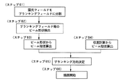
(ステップ61)
図4に示すように、電子ビームを用いて露光すべき基板内の露光フィールド701を複数の小領域であるブランキングフィールド702に分割する。図4では露光すべきフィールドを4×4のブランキングフィールドに分割している。露光フィールド701をブランキングフィールド702に分割後、ステップ62に移行する。
(ステップ62)
各ブランキングフィールド702の中心位置もしくは最大偏向位置でのビーム形状を検出する。全ブランキングフィールド702でのビーム形状を検出後、ステップ63に移行する。
(ステップ63)
各ブランキングフィールド702でのビーム形状からビーム径が最も短くなる方向を算出する。全ブランキングフィールド702でのビーム短径方向を算出後、ステップ65に移行する。
(ステップ64)
あらかじめ収差計算等から求めたビーム径から、ビーム径が最も短くなる方向を算出する。全ブランキングフィールド702でのビーム短径方向を算出後、ステップ65に移行する。
(ステップ65)
ステップ4もしくはステップ5から、ビーム径が最も短くなる方向を各ブランキングフィールドのブランキング方向として決定する。全ブランキングフィールド702でのブランキング方向を決定後、ステップ66に移行する。
(ステップ66)
各ブランキングフィールドに電子ビームが偏向されたとき、ステップ65で決定したブランキング方向に電子ビームをブランキングしながら描画を行う。
[Second Embodiment]
(2) Electron beam exposure apparatus that performs blanking in the direction of the shortest beam diameter (when using one electron beam)
The operation of the electron beam exposure apparatus of this embodiment will be described with reference to FIG.
(Step 61)
As shown in FIG. 4, an
(Step 62)
The beam shape at the center position or maximum deflection position of each
(Step 63)
The direction in which the beam diameter becomes the shortest is calculated from the beam shape in each blanking
(Step 64)
The direction in which the beam diameter becomes the shortest is calculated from the beam diameter previously obtained from aberration calculation or the like. After calculating the beam minor axis direction in all blanking
(Step 65)
From step 4 or step 5, the direction in which the beam diameter becomes the shortest is determined as the blanking direction of each blanking field. After determining the blanking direction in all blanking
(Step 66)
When the electron beam is deflected in each blanking field, drawing is performed while blanking the electron beam in the blanking direction determined in step 65.
以上の動作ステップを行うことで、もともと電子ビームが持っている像高に依存した非点収差やコマ収差によるぼけと、ブランキングによる電子ビームのぼけと、を相殺することができ、描画パターンの寸法精度を向上させることが出来る。 By performing the above operation steps, the blur due to astigmatism and coma depending on the image height originally possessed by the electron beam and the blur of the electron beam due to blanking can be canceled. Dimensional accuracy can be improved.
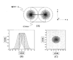
図5に、電子ビームのぼけの方向とブランキング方向の計算による比較結果を示す。 図5(A)は、もともとの電子ビームのビーム径が最も長くなる方向とブランキング方向を一致させた場合のパターン寸法精度のグラフである。図5(B)は、もともとの電子ビームのビーム径が最も短くなる方向とブランキング方向を一致させた場合のパターン寸法精度のグラフである。
横軸はフォーカスのずれ量、縦軸はパターン寸法精度を示している。+2ミクロンのフォーカスのずれがある場合、パターン寸法精度が4倍以上向上していることが分かる。
つまり、ブランキング手段を用いて基板を露光する電子ビーム露光装置において、ブランキングの方向をあらかじめ決められた方向に調整する機能を有することで、パターン寸法精度を向上することが出来る。
FIG. 5 shows a comparison result obtained by calculating the direction of blur of the electron beam and the blanking direction. FIG. 5A is a graph of pattern dimensional accuracy when the direction in which the beam diameter of the original electron beam is the longest and the blanking direction are matched. FIG. 5B is a graph of pattern dimensional accuracy when the direction in which the beam diameter of the original electron beam is the shortest and the blanking direction are matched.
The horizontal axis indicates the focus shift amount, and the vertical axis indicates the pattern dimension accuracy. It can be seen that when there is a focus shift of +2 microns, the pattern dimensional accuracy is improved by 4 times or more.
In other words, the electron beam exposure apparatus that exposes the substrate using the blanking means has a function of adjusting the blanking direction to a predetermined direction, thereby improving the pattern dimension accuracy.
[第3の実施例]
(3)ビーム径が最も短い方向にブランキングを行う電子ビーム露光装置
(複数の電子ビームを用いる場合)
図6は本発明に係るマルチビーム方式の電子ビーム露光装置の要部概略図である。 901から909は複数の電子源像を形成し、その電子源像から電子ビームを放射するマルチソースモジュールで、図6の場合、マルチソースモジュールは5×5の25個が2次元配列されている。901は、電子銃が形成する電子源(クロスオーバー像)である。この電子源901から放射される電子ビームは、コンデンサーレンズ902によって略平行な電子ビームとなる。903は、開孔が2次元配列して形成されたアパーチャアレイ、904は、同一の光学パワーを有する静電レンズが2次元配列して形成されたレンズアレイ、905、906、907、908は、個別に駆動可能な静電偏向器が2次元配列して形成されたマルチ偏向器アレイ、909は、個別に駆動可能な静電のブランカーが2次元配列して形成されたブランカーアレイである。
[Third embodiment]
(3) Electron beam exposure apparatus that performs blanking in the direction with the shortest beam diameter (when using multiple electron beams)
FIG. 6 is a schematic view of a main part of a multi-beam type electron beam exposure apparatus according to the present invention.
図7を用いて各機能を説明する。コンデンサーレンズ902からの略平行な電子ビームは、アパーチャアレイ903によって複数の電子ビームに分割される。分割された電子ビームは、対応するレンズアレイ904の静電レンズを介して、ブランカーアレイ909の対応するブランカー上に、電子源901の中間像1001を形成する。この時、マルチ偏向器アレイ905、906、907、908は、ブランカーアレイ909上に形成される
電子源の中間像1001の位置(光軸と直交する面内の位置)を個別に調整する。また、ブランカーアレイ909で偏向された電子ビームは、図6のブランキングアパーチャ910によって遮断されるため、ウエハ920には照射されない。一方、ブランカーアレイ909で偏向されない電子ビームは、図6のブランキングアパーチャ910によって遮断されないため、ウエハ920には照射される。
Each function will be described with reference to FIG. The substantially parallel electron beam from the
図6に戻り、マルチソースモジュールで形成された電子源の複数の中間像は、磁界レンズ915、916、917、918の縮小投影系を介して、ウエハ920に投影される。この時、複数の中間像がウエハ920に投影される際、焦点位置は、ダイナミックフォーカスレンズ(静電もしくは磁界レンズ)911、912で調整できる。913、914は各電子ビームを露光すべき個所へ偏向させる主偏向器と副偏向器である。919はウエハ920上に形成された電子源の各中間像の位置を計測するための反射電子検出器である。921はウエハを移動させるためのステージである。922は電子ビームの位置およびビーム形状を検出するためのマークである。
Returning to FIG. 6, a plurality of intermediate images of the electron source formed by the multi-source module are projected onto the
図8を用いて本実施例の電子ビーム露光装置の動作について説明する。
(ステップ111)
複数の電子ビーム一本毎のビーム形状を検出する。全電子ビームのビーム形状を検出後、ステップ112に移行する。
(ステップ112)
各電子ビームの形状からビーム径が最も短くなる方向を算出する。全電子ビームの短径方向を算出後、ステップ113もしくはステップ114に移行する。
(ステップ113)
ビーム径が最も短くなる方向を、電子ビーム1本毎にブランキング方向として決定する。電子ビーム1本毎のブランキング方向を決定後、ステップ115に移行する。(ステップ114)
あらかじめ決められた近接電子ビーム複数本の中心位置もしくは最大軸外位置にある電子ビームのビーム径が最も短くなる方向を、近接電子ビーム複数本のブランキング方向として決定する。近接電子ビーム複数本のブランキング方向を決定後、ステップ115に移行する。
(ステップ115)
各電子ビームをステップ113もしくはステップ114で決定したブランキング方向に電子ビームをブランキングしながら描画を行う。
The operation of the electron beam exposure apparatus of this embodiment will be described with reference to FIG.
(Step 111)
A beam shape for each of a plurality of electron beams is detected. After the beam shapes of all electron beams are detected, the process proceeds to step 112.
(Step 112)
The direction in which the beam diameter is the shortest is calculated from the shape of each electron beam. After calculating the minor axis direction of all electron beams, the process proceeds to step 113 or step 114.
(Step 113)
The direction in which the beam diameter is the shortest is determined as the blanking direction for each electron beam. After determining the blanking direction for each electron beam, the process proceeds to step 115. (Step 114)
The direction in which the beam diameter of the electron beam at the center position or the maximum off-axis position of the plurality of adjacent electron beams determined in advance is the shortest is determined as the blanking direction of the plurality of adjacent electron beams. After determining the blanking directions of a plurality of adjacent electron beams, the process proceeds to step 115.
(Step 115)
Drawing is performed while blanking each electron beam in the blanking direction determined in step 113 or step 114.
以上の動作ステップを行うことで、複数の電子ビームが各々持っているビームのぼけとブランキングによる電子ビームのぼけとを相殺することができ、複数の電子ビームによる描画パターンの寸法精度を向上させることが出来る。つまり、ブランキング手段を用いて基板を露光する電子ビーム露光装置において、ブランキングの方向をあらかじめ決められた方向に調整する機能を有することで、パターン寸法精度を向上することが出来る。 By performing the above operation steps, it is possible to cancel the beam blur of each of the plurality of electron beams and the blur of the electron beam due to blanking, thereby improving the dimensional accuracy of the drawing pattern by the plurality of electron beams. I can do it. In other words, the electron beam exposure apparatus that exposes the substrate using the blanking means has a function of adjusting the blanking direction to a predetermined direction, thereby improving the pattern dimension accuracy.
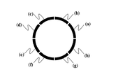
なお、上記実施例において、ブランカーとしての偏向器は、偏向電極を複数対有し、荷電粒子線を光軸回りの360度方向に偏向可能なものを用いることが好ましい。
例として、8極子偏向器を上から見た図を図14に示す。
例えばY方向の正側に電子ビームを変更したい場合には、8極の電極(a)から(h)それぞれに、(a)(√2−1)Vy、(b)Vy、(c)Vy、(d)(√2−1)Vy、(e)−(√2−1)Vy、(f)−Vy、(g)−Vy、(h)−(√2−1)Vyの電圧を印加する。ただしVyは任意の電圧である。
ブランキングの際に用いるブランカーは、12極子偏向器でも20極子偏向器でも良い。
In the above-described embodiment, it is preferable to use a deflector as a blanker that has a plurality of pairs of deflection electrodes and can deflect a charged particle beam in a 360-degree direction around the optical axis.
As an example, FIG. 14 shows a view of an octupole deflector viewed from above.
For example, when it is desired to change the electron beam to the positive side in the Y direction, (a) (√2-1) Vy, (b) Vy, (c) Vy are respectively applied to the eight-pole electrodes (a) to (h). , (D) (√2-1) Vy, (e)-(√2-1) Vy, (f) -Vy, (g) -Vy, (h)-(√2-1) Vy Apply. However, Vy is an arbitrary voltage.
The blanker used for blanking may be a 12-pole deflector or a 20-pole deflector.
また、偏向電極を一対しか持たず、光軸と垂直な1つの直線方向にしか荷電粒子線を偏向できないものを用いる場合にも本発明は適用可能である。この場合、調整手段は、ブランカーを光軸回りに回転させることにより、ブランキング方向を調整する。または、一対の偏向電極を多段並べて、ブランキング方向を増やしても良い。また、複数ビームを用いる場合は、ブランカーを光軸回りに90度回転させるものであってもよい。さらに、ラスタースキャンを行う装置では、荷電粒子線のスキャン方向と必要に応じて基板の向きを調整してもよい。 The present invention can also be applied to a case where only one pair of deflection electrodes is provided and a charged particle beam can be deflected only in one linear direction perpendicular to the optical axis. In this case, the adjusting means adjusts the blanking direction by rotating the blanker around the optical axis. Alternatively, the blanking direction may be increased by arranging a plurality of pairs of deflection electrodes. When using a plurality of beams, the blanker may be rotated 90 degrees around the optical axis. Furthermore, in a raster scanning apparatus, the charged particle beam scanning direction and the orientation of the substrate may be adjusted as necessary.
[第4の実施例]
次に以上説明した電子ビーム露光装置を利用したデバイスの生産方法の実施例を説明する。
図9に微小デバイス(ICやLSI等の半導体チップ、液晶パネル、CCD、薄膜磁気ヘッド、マイクロマシン等)の製造のフローを示す。ステップ121(回路設計)では半導体デバイスの回路設計を行う。ステップ122(EBデータ変換)では設計した回路パターンに基づいて露光装置の露光制御データを作成する。一方、ステップ123(ウエハ製造)ではシリコン等の材料を用いてウエハを製造する。ステップ124(ウエハプロセス)は前工程と呼ばれ、上記用意した露光制御データが入力された露光装置とウエハを用いて、リソグラフィ技術によってウエハ上に実際の回路を形成する。次のステップ125(組み立て)は後工程と呼ばれ、ステップ124によって作製されたウエハを用いて半導体チップ化する工程であり、アッセンブリ工程(ダイシング、ボンディング)、パッケージング工程(チップ封入)等の工程を含む。ステップ126(検査)ではステップ125で作製された半導体デバイスの動作確認テスト、耐久性テスト等の検査を行う。こうした工程を経て半導体デバイスが完成し、これが出荷(ステップ127)される。
[Fourth embodiment]
Next, an embodiment of a device production method using the electron beam exposure apparatus described above will be described.
FIG. 9 shows a flow of manufacturing a microdevice (a semiconductor chip such as an IC or LSI, a liquid crystal panel, a CCD, a thin film magnetic head, a micromachine, etc.). In step 121 (circuit design), a semiconductor device circuit is designed. In step 122 (EB data conversion), exposure control data for the exposure apparatus is created based on the designed circuit pattern. On the other hand, in step 123 (wafer manufacture), a wafer is manufactured using a material such as silicon. Step 124 (wafer process) is called a pre-process, and an actual circuit is formed on the wafer by lithography using the wafer and the exposure apparatus to which the prepared exposure control data is input. The next step 125 (assembly) is referred to as a post-process, and is a process of forming a semiconductor chip using the wafer produced in step 124, and is a process such as an assembly process (dicing, bonding), a packaging process (chip encapsulation), or the like. including. In step 126 (inspection), inspections such as an operation check test and a durability test of the semiconductor device manufactured in step 125 are performed. Through these steps, a semiconductor device is completed and shipped (step 127).
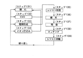
図10は上記ウエハプロセスの詳細なフローを示す。ステップ131(酸化)ではウエハの表面を酸化させる。ステップ132(CVD)ではウエハ表面に絶縁膜を形成する。ステップ133(電極形成)ではウエハ上に電極を蒸着によって形成する。ステップ134(イオン打込み)ではウエハにイオンを打ち込む。ステップ135(レジスト処理)ではウエハに感光剤を塗布する。ステップ136(露光)では上記説明した露光装置によって回路パターンをウエハに焼付露光する。ステップ137(現像)では露光したウエハを現像する。ステップ138(エッチング)では現像したレジスト像以外の部分を削り取る。ステップ139(レジスト剥離)ではエッチングが済んで不要となったレジストを取り除く。これらのステップを繰り返し行うことによって、ウエハ上に多重に回路パターンが形成される。 本実施例の製造方法を用いれば、高集積度の半導体デバイスをパターン寸法精度良く製造することが出来る。 FIG. 10 shows a detailed flow of the wafer process. In step 131 (oxidation), the wafer surface is oxidized. In step 132 (CVD), an insulating film is formed on the wafer surface. In step 133 (electrode formation), an electrode is formed on the wafer by vapor deposition. In step 134 (ion implantation), ions are implanted into the wafer. In step 135 (resist processing), a photosensitive agent is applied to the wafer. In step 136 (exposure), the circuit pattern is printed on the wafer by exposure using the exposure apparatus described above. In step 137 (development), the exposed wafer is developed. In step 138 (etching), portions other than the developed resist image are removed. In step 139 (resist stripping), the resist that has become unnecessary after the etching is removed. By repeatedly performing these steps, multiple circuit patterns are formed on the wafer. By using the manufacturing method of this embodiment, a highly integrated semiconductor device can be manufactured with high pattern dimension accuracy.
101 電子源
102 電磁レンズ
103 電子源の像
104 ブランカー
105 電磁レンズ
106 電磁レンズ
107 静電偏向器
108 電磁レンズ
109 ウエハ
201 ピクセル
202 電子ビーム
203 描画すべきピクセル
701 露光フィールド
702 ブランキングフィールド
901 電子源(クロスオーバー像)
902 コンデンサーレンズ
903 アパーチャアレイ
904 レンズアレイ
905 マルチ偏向器アレイ
906 マルチ偏向器アレイ
907 マルチ偏向器アレイ
908 マルチ偏向器アレイ
909 ブランカーアレイ
910 ブランキングアパーチャ
911 ダイナミックフォーカスレンズ
912 ダイナミックフォーカスレンズ
913 主偏向器
914 副偏向器
915 磁界レンズ
916 磁界レンズ
917 磁界レンズ
918 磁界レンズ
919 反射電子検出器
920 ウエハ
921 ステージ
922 マーク
1001 電子源の中間像
DESCRIPTION OF
902
Claims (1)
前記荷電粒子線を偏向可能な偏向器を有し、前記荷電粒子線を偏向して前記被露光基板への照射を制御するブランキング手段と、
前記偏向器による前記荷電粒子線のブランキング方向を調整する調整手段と、
前記被露光基板に対して前記荷電粒子線を走査させる走査手段と、を備え、
前記ブランキング手段は、前記荷電粒子線を通過させるためのブランキングアパーチャを有し、
前記偏向器は、前記ブランキングアパーチャを挟んで異なる4つの方向に配置された4対の電極を含み、前記荷電粒子線を少なくとも4つの方向に偏向可能であり、
前記調整手段は、前記荷電粒子線のブランキング方向を前記荷電粒子線の走査方向と垂直な方向に調整することを特徴とする荷電粒子線露光装置。 A charged particle beam exposure apparatus that exposes a pattern on a substrate to be exposed using a charged particle beam,
Blanking means for deflecting the charged particle beam and deflecting the charged particle beam to control irradiation to the substrate to be exposed;
Adjusting means for adjusting a blanking direction of the charged particle beam by the deflector ;
Scanning means for scanning the charged particle beam with respect to the substrate to be exposed ,
The blanking means has a blanking aperture for passing the charged particle beam,
The deflector includes four pairs of electrodes arranged in four different directions across the blanking aperture, and is capable of deflecting the charged particle beam in at least four directions,
The charged particle beam exposure apparatus , wherein the adjusting unit adjusts a blanking direction of the charged particle beam in a direction perpendicular to a scanning direction of the charged particle beam.
Priority Applications (2)
| Application Number | Priority Date | Filing Date | Title |
|---|---|---|---|
| JP2004194775A JP4477436B2 (en) | 2004-06-30 | 2004-06-30 | Charged particle beam exposure system |
| US11/159,356 US7173262B2 (en) | 2004-06-30 | 2005-06-23 | Charged particle beam exposure apparatus, charged particle beam exposure method and device manufacturing method |
Applications Claiming Priority (1)
| Application Number | Priority Date | Filing Date | Title |
|---|---|---|---|
| JP2004194775A JP4477436B2 (en) | 2004-06-30 | 2004-06-30 | Charged particle beam exposure system |
Publications (3)
| Publication Number | Publication Date |
|---|---|
| JP2006019439A JP2006019439A (en) | 2006-01-19 |
| JP2006019439A5 JP2006019439A5 (en) | 2007-08-16 |
| JP4477436B2 true JP4477436B2 (en) | 2010-06-09 |
Family
ID=35656178
Family Applications (1)
| Application Number | Title | Priority Date | Filing Date |
|---|---|---|---|
| JP2004194775A Expired - Fee Related JP4477436B2 (en) | 2004-06-30 | 2004-06-30 | Charged particle beam exposure system |
Country Status (2)
| Country | Link |
|---|---|
| US (1) | US7173262B2 (en) |
| JP (1) | JP4477436B2 (en) |
Families Citing this family (7)
| Publication number | Priority date | Publication date | Assignee | Title |
|---|---|---|---|---|
| JP4559137B2 (en) * | 2004-06-30 | 2010-10-06 | キヤノン株式会社 | Vacuum equipment manufacturing apparatus and manufacturing method |
| JP4477436B2 (en) * | 2004-06-30 | 2010-06-09 | キヤノン株式会社 | Charged particle beam exposure system |
| US7770180B2 (en) * | 2004-12-21 | 2010-08-03 | Microsoft Corporation | Exposing embedded data in a computer-generated document |
| JP4657740B2 (en) * | 2005-01-26 | 2011-03-23 | キヤノン株式会社 | Aberration measuring apparatus for charged particle beam optical system, charged particle beam exposure apparatus including the aberration measuring apparatus, and device manufacturing method using the apparatus |
| JP2008004596A (en) * | 2006-06-20 | 2008-01-10 | Canon Inc | Charged particle beam drawing method, aligner, and process for fabricating device |
| JP5199921B2 (en) * | 2009-03-06 | 2013-05-15 | 株式会社ニューフレアテクノロジー | Charged particle beam drawing apparatus and optical axis deviation correction method for charged particle beam |
| CN111527582B (en) * | 2017-10-02 | 2023-12-29 | Asml荷兰有限公司 | Apparatus using charged particle beam |
Family Cites Families (19)
| Publication number | Priority date | Publication date | Assignee | Title |
|---|---|---|---|---|
| US5262341A (en) * | 1989-05-19 | 1993-11-16 | Fujitsu Limited | Blanking aperture array and charged particle beam exposure method |
| EP0404608B1 (en) * | 1989-05-19 | 1995-02-22 | Fujitsu Limited | Blanking aperture array, method of producing blanking aperture array, charged particle beam exposure apparatus and charged particle beam exposure method |
| EP0508151B1 (en) * | 1991-03-13 | 1998-08-12 | Fujitsu Limited | Charged particle beam exposure system and charged particle beam exposure method |
| US5528048A (en) * | 1994-03-15 | 1996-06-18 | Fujitsu Limited | Charged particle beam exposure system and method |
| JP3299632B2 (en) * | 1994-06-24 | 2002-07-08 | 株式会社日立製作所 | Electron beam drawing equipment |
| JP3647136B2 (en) | 1996-04-23 | 2005-05-11 | キヤノン株式会社 | Electron beam exposure system |
| JPH09240143A (en) | 1996-03-04 | 1997-09-16 | Mitsubishi Paper Mills Ltd | Color developing type reversible heat-sensitive recording material and its manufacture |
| JP3647143B2 (en) | 1996-06-12 | 2005-05-11 | キヤノン株式会社 | Electron beam exposure apparatus and exposure method therefor |
| JPH09330868A (en) | 1996-06-12 | 1997-12-22 | Canon Inc | Electron beam exposure method and manufacture of device using it |
| JP3647128B2 (en) | 1996-03-04 | 2005-05-11 | キヤノン株式会社 | Electron beam exposure apparatus and exposure method thereof |
| US5834783A (en) | 1996-03-04 | 1998-11-10 | Canon Kabushiki Kaisha | Electron beam exposure apparatus and method, and device manufacturing method |
| JP4647820B2 (en) * | 2001-04-23 | 2011-03-09 | キヤノン株式会社 | Charged particle beam drawing apparatus and device manufacturing method |
| JP3940310B2 (en) * | 2002-04-04 | 2007-07-04 | 株式会社日立ハイテクノロジーズ | Electron beam drawing method, drawing apparatus, and semiconductor manufacturing method using the same |
| US6818911B2 (en) * | 2002-04-10 | 2004-11-16 | Canon Kabushiki Kaisha | Array structure and method of manufacturing the same, charged particle beam exposure apparatus, and device manufacturing method |
| JP4167904B2 (en) * | 2003-01-06 | 2008-10-22 | 株式会社日立ハイテクノロジーズ | Electron beam drawing apparatus and electron beam drawing method |
| JP4421836B2 (en) * | 2003-03-28 | 2010-02-24 | キヤノン株式会社 | Exposure apparatus and device manufacturing method |
| JP4313145B2 (en) * | 2003-10-07 | 2009-08-12 | 株式会社日立ハイテクノロジーズ | Charged particle beam drawing method and charged particle beam drawing apparatus |
| JP4477436B2 (en) * | 2004-06-30 | 2010-06-09 | キヤノン株式会社 | Charged particle beam exposure system |
| JP4907092B2 (en) * | 2005-03-01 | 2012-03-28 | 株式会社日立ハイテクノロジーズ | Electron beam drawing apparatus and electron beam drawing method |
-
2004
- 2004-06-30 JP JP2004194775A patent/JP4477436B2/en not_active Expired - Fee Related
-
2005
- 2005-06-23 US US11/159,356 patent/US7173262B2/en active Active
Also Published As
| Publication number | Publication date |
|---|---|
| US20060017019A1 (en) | 2006-01-26 |
| US7173262B2 (en) | 2007-02-06 |
| JP2006019439A (en) | 2006-01-19 |
Similar Documents
| Publication | Publication Date | Title |
|---|---|---|
| US6903353B2 (en) | Charged particle beam exposure apparatus, device manufacturing method, and charged particle beam applied apparatus | |
| US6472672B1 (en) | Electron beam exposure apparatus and its control method | |
| JP3787417B2 (en) | Electron beam exposure method and electron beam exposure apparatus | |
| US7005658B2 (en) | Charged particle beam exposure apparatus and method | |
| US5939725A (en) | Electron beam exposure apparatus | |
| JPH1064812A (en) | Electronic beam exposure method and device manufacturing method using it | |
| US7173262B2 (en) | Charged particle beam exposure apparatus, charged particle beam exposure method and device manufacturing method | |
| JPH09288991A (en) | Electron beam exposing device | |
| US7049610B2 (en) | Charged particle beam exposure method, charged particle beam exposure apparatus, and device manufacturing method | |
| US7005659B2 (en) | Charged particle beam exposure apparatus, charged particle beam exposure method, and device manufacturing method using the same apparatus | |
| JP3647143B2 (en) | Electron beam exposure apparatus and exposure method therefor | |
| JP4804136B2 (en) | Charged particle beam apparatus and device manufacturing method | |
| JP3832914B2 (en) | Electron beam exposure apparatus and device manufacturing method using the apparatus | |
| JP4143204B2 (en) | Charged particle beam exposure apparatus and device manufacturing method using the apparatus | |
| JP3976835B2 (en) | Electron beam exposure method and electron beam exposure apparatus | |
| JP3919255B2 (en) | Electron beam exposure apparatus and device manufacturing method | |
| JP4356064B2 (en) | Charged particle beam exposure apparatus and device manufacturing method using the apparatus | |
| JP3673608B2 (en) | Electron beam illumination apparatus and electron beam exposure apparatus equipped with the apparatus | |
| JP3728315B2 (en) | Electron beam exposure apparatus, electron beam exposure method, and device manufacturing method | |
| JP4494734B2 (en) | Charged particle beam drawing method, charged particle beam exposure apparatus, and device manufacturing method | |
| JPH10308340A (en) | Electron beam exposing method and device | |
| JP4006054B2 (en) | Electron beam exposure system | |
| JP2007019193A (en) | Charged particle beam equipment, method for regulating lens power, and process for fabricating device | |
| JPH09330868A (en) | Electron beam exposure method and manufacture of device using it | |
| JPH09330869A (en) | Position detector and electron beam aligner with it |
Legal Events
| Date | Code | Title | Description |
|---|---|---|---|
| A521 | Request for written amendment filed |
Free format text: JAPANESE INTERMEDIATE CODE: A523 Effective date: 20070627 |
|
| A621 | Written request for application examination |
Free format text: JAPANESE INTERMEDIATE CODE: A621 Effective date: 20070627 |
|
| RD03 | Notification of appointment of power of attorney |
Free format text: JAPANESE INTERMEDIATE CODE: A7423 Effective date: 20090413 |
|
| RD03 | Notification of appointment of power of attorney |
Free format text: JAPANESE INTERMEDIATE CODE: A7423 Effective date: 20090709 |
|
| A131 | Notification of reasons for refusal |
Free format text: JAPANESE INTERMEDIATE CODE: A131 Effective date: 20091002 |
|
| A521 | Request for written amendment filed |
Free format text: JAPANESE INTERMEDIATE CODE: A523 Effective date: 20091201 |
|
| TRDD | Decision of grant or rejection written | ||
| A01 | Written decision to grant a patent or to grant a registration (utility model) |
Free format text: JAPANESE INTERMEDIATE CODE: A01 Effective date: 20100212 |
|
| A01 | Written decision to grant a patent or to grant a registration (utility model) |
Free format text: JAPANESE INTERMEDIATE CODE: A01 |
|
| A61 | First payment of annual fees (during grant procedure) |
Free format text: JAPANESE INTERMEDIATE CODE: A61 Effective date: 20100311 |
|
| R150 | Certificate of patent or registration of utility model |
Ref document number: 4477436 Country of ref document: JP Free format text: JAPANESE INTERMEDIATE CODE: R150 Free format text: JAPANESE INTERMEDIATE CODE: R150 |
|
| FPAY | Renewal fee payment (event date is renewal date of database) |
Free format text: PAYMENT UNTIL: 20130319 Year of fee payment: 3 |
|
| FPAY | Renewal fee payment (event date is renewal date of database) |
Free format text: PAYMENT UNTIL: 20130319 Year of fee payment: 3 |
|
| FPAY | Renewal fee payment (event date is renewal date of database) |
Free format text: PAYMENT UNTIL: 20140319 Year of fee payment: 4 |
|
| R250 | Receipt of annual fees |
Free format text: JAPANESE INTERMEDIATE CODE: R250 |
|
| R250 | Receipt of annual fees |
Free format text: JAPANESE INTERMEDIATE CODE: R250 |
|
| R250 | Receipt of annual fees |
Free format text: JAPANESE INTERMEDIATE CODE: R250 |
|
| R250 | Receipt of annual fees |
Free format text: JAPANESE INTERMEDIATE CODE: R250 |
|
| R250 | Receipt of annual fees |
Free format text: JAPANESE INTERMEDIATE CODE: R250 |
|
| R250 | Receipt of annual fees |
Free format text: JAPANESE INTERMEDIATE CODE: R250 |
|
| R250 | Receipt of annual fees |
Free format text: JAPANESE INTERMEDIATE CODE: R250 |
|
| S531 | Written request for registration of change of domicile |
Free format text: JAPANESE INTERMEDIATE CODE: R313531 |
|
| S533 | Written request for registration of change of name |
Free format text: JAPANESE INTERMEDIATE CODE: R313533 |
|
| LAPS | Cancellation because of no payment of annual fees | ||
| R350 | Written notification of registration of transfer |
Free format text: JAPANESE INTERMEDIATE CODE: R350 |