JP2008004596A - Charged particle beam drawing method, aligner, and process for fabricating device - Google Patents
Charged particle beam drawing method, aligner, and process for fabricating device Download PDFInfo
- Publication number
- JP2008004596A JP2008004596A JP2006169797A JP2006169797A JP2008004596A JP 2008004596 A JP2008004596 A JP 2008004596A JP 2006169797 A JP2006169797 A JP 2006169797A JP 2006169797 A JP2006169797 A JP 2006169797A JP 2008004596 A JP2008004596 A JP 2008004596A
- Authority
- JP
- Japan
- Prior art keywords
- charged particle
- pattern
- particle beam
- dose
- wafer
- Prior art date
- Legal status (The legal status is an assumption and is not a legal conclusion. Google has not performed a legal analysis and makes no representation as to the accuracy of the status listed.)
- Pending
Links
Images


Classifications
-
- H—ELECTRICITY
- H01—ELECTRIC ELEMENTS
- H01J—ELECTRIC DISCHARGE TUBES OR DISCHARGE LAMPS
- H01J37/00—Discharge tubes with provision for introducing objects or material to be exposed to the discharge, e.g. for the purpose of examination or processing thereof
- H01J37/30—Electron-beam or ion-beam tubes for localised treatment of objects
- H01J37/304—Controlling tubes by information coming from the objects or from the beam, e.g. correction signals
-
- B—PERFORMING OPERATIONS; TRANSPORTING
- B82—NANOTECHNOLOGY
- B82Y—SPECIFIC USES OR APPLICATIONS OF NANOSTRUCTURES; MEASUREMENT OR ANALYSIS OF NANOSTRUCTURES; MANUFACTURE OR TREATMENT OF NANOSTRUCTURES
- B82Y10/00—Nanotechnology for information processing, storage or transmission, e.g. quantum computing or single electron logic
-
- B—PERFORMING OPERATIONS; TRANSPORTING
- B82—NANOTECHNOLOGY
- B82Y—SPECIFIC USES OR APPLICATIONS OF NANOSTRUCTURES; MEASUREMENT OR ANALYSIS OF NANOSTRUCTURES; MANUFACTURE OR TREATMENT OF NANOSTRUCTURES
- B82Y40/00—Manufacture or treatment of nanostructures
-
- H—ELECTRICITY
- H01—ELECTRIC ELEMENTS
- H01J—ELECTRIC DISCHARGE TUBES OR DISCHARGE LAMPS
- H01J37/00—Discharge tubes with provision for introducing objects or material to be exposed to the discharge, e.g. for the purpose of examination or processing thereof
- H01J37/30—Electron-beam or ion-beam tubes for localised treatment of objects
- H01J37/317—Electron-beam or ion-beam tubes for localised treatment of objects for changing properties of the objects or for applying thin layers thereon, e.g. for ion implantation
- H01J37/3174—Particle-beam lithography, e.g. electron beam lithography
-
- H—ELECTRICITY
- H01—ELECTRIC ELEMENTS
- H01J—ELECTRIC DISCHARGE TUBES OR DISCHARGE LAMPS
- H01J2237/00—Discharge tubes exposing object to beam, e.g. for analysis treatment, etching, imaging
- H01J2237/04—Means for controlling the discharge
- H01J2237/043—Beam blanking
-
- H—ELECTRICITY
- H01—ELECTRIC ELEMENTS
- H01J—ELECTRIC DISCHARGE TUBES OR DISCHARGE LAMPS
- H01J2237/00—Discharge tubes exposing object to beam, e.g. for analysis treatment, etching, imaging
- H01J2237/245—Detection characterised by the variable being measured
- H01J2237/24507—Intensity, dose or other characteristics of particle beams or electromagnetic radiation
-
- H—ELECTRICITY
- H01—ELECTRIC ELEMENTS
- H01J—ELECTRIC DISCHARGE TUBES OR DISCHARGE LAMPS
- H01J2237/00—Discharge tubes exposing object to beam, e.g. for analysis treatment, etching, imaging
- H01J2237/30—Electron or ion beam tubes for processing objects
- H01J2237/304—Controlling tubes
- H01J2237/30433—System calibration
- H01J2237/3045—Deflection calibration
-
- H—ELECTRICITY
- H01—ELECTRIC ELEMENTS
- H01J—ELECTRIC DISCHARGE TUBES OR DISCHARGE LAMPS
- H01J2237/00—Discharge tubes exposing object to beam, e.g. for analysis treatment, etching, imaging
- H01J2237/30—Electron or ion beam tubes for processing objects
- H01J2237/304—Controlling tubes
- H01J2237/30455—Correction during exposure
-
- H—ELECTRICITY
- H01—ELECTRIC ELEMENTS
- H01J—ELECTRIC DISCHARGE TUBES OR DISCHARGE LAMPS
- H01J2237/00—Discharge tubes exposing object to beam, e.g. for analysis treatment, etching, imaging
- H01J2237/30—Electron or ion beam tubes for processing objects
- H01J2237/304—Controlling tubes
- H01J2237/30472—Controlling the beam
- H01J2237/30477—Beam diameter
-
- H—ELECTRICITY
- H01—ELECTRIC ELEMENTS
- H01J—ELECTRIC DISCHARGE TUBES OR DISCHARGE LAMPS
- H01J2237/00—Discharge tubes exposing object to beam, e.g. for analysis treatment, etching, imaging
- H01J2237/30—Electron or ion beam tubes for processing objects
- H01J2237/304—Controlling tubes
- H01J2237/30472—Controlling the beam
- H01J2237/30483—Scanning
Landscapes
- Chemical & Material Sciences (AREA)
- Engineering & Computer Science (AREA)
- Nanotechnology (AREA)
- Analytical Chemistry (AREA)
- Physics & Mathematics (AREA)
- Crystallography & Structural Chemistry (AREA)
- Manufacturing & Machinery (AREA)
- General Physics & Mathematics (AREA)
- Condensed Matter Physics & Semiconductors (AREA)
- Mathematical Physics (AREA)
- Theoretical Computer Science (AREA)
- Exposure And Positioning Against Photoresist Photosensitive Materials (AREA)
- Electron Beam Exposure (AREA)
Abstract
Description
本発明は、電子線を例えばラスタースキャンして描画を行う荷電粒子線描画方法に関し、かつ、その荷電粒子線描画方法を用いた露光装置、及びデバイス製造方法に関する。 The present invention relates to a charged particle beam drawing method that performs drawing by, for example, raster scanning an electron beam, and to an exposure apparatus and a device manufacturing method using the charged particle beam drawing method.
従来より、例えば荷電粒子線をラスタースキャンすることによって、微細かつ高集積率の例えば半導体集積回路等の製作を可能にするという技術が一般に利用されている。
例えば特開2005−32838号公報により、基板上の荷電粒子線のラスタースキャン方向の大きさを、前記ラスター方向と直交する方向の大きさに比べ狭める調整を行うという荷電粒子線描画方法が知られている(特許文献1参照)。
この荷電粒子線描画方法は、ラスタースキャン型の電子ビームを出力する電子線露光装置に適用することが可能である。
2. Description of the Related Art Conventionally, a technique that enables fabrication of, for example, a semiconductor integrated circuit having a fine and high integration rate, for example, by raster scanning a charged particle beam has been generally used.
For example, Japanese Patent Laid-Open No. 2005-32838 discloses a charged particle beam drawing method in which the size of a charged particle beam on a substrate is adjusted to be narrower than the size in a direction perpendicular to the raster direction. (See Patent Document 1).
This charged particle beam drawing method can be applied to an electron beam exposure apparatus that outputs a raster scan type electron beam.
一方、図13は、従来の一般的なラスタースキャン型の電子線露光装置の一構成例を説明する説明図である。
従来のラスタースキャン型の電子線露光装置は、まず、電子源Sから電子ビームを照射する。その電子ビームは、電子レンズL1によって、電子源Sの像を形成する。
その電子減Sの像は、電子レンズL2,L3で構成される縮小電子光学系を介して、ウエハWに縮小投影される。
ブランカーBは、電子レンズL1によって形成される電子源Sの像の位置にある静電型偏向器であり、電子ビームのウエハW上への照射、非照射を制御する。
即ち、例えば電子ビームをウエハWに照射させない場合は、電子ビームを偏向させて、縮小電子光学系の瞳上に位置するブランキングアパーチャBAで、電子ビームを遮断する。また、電子ビームは、静電型偏向器DEFによってウエハW上を走査される。
On the other hand, FIG. 13 is an explanatory diagram for explaining a configuration example of a conventional general raster scan type electron beam exposure apparatus.
A conventional raster scan type electron beam exposure apparatus first irradiates an electron beam from an electron source S. The electron beam forms an image of the electron source S by the electron lens L1.
The image of the electron reduction S is reduced and projected onto the wafer W through a reduction electron optical system constituted by the electron lenses L2 and L3.
The blanker B is an electrostatic deflector located at the position of the image of the electron source S formed by the electron lens L1, and controls irradiation and non-irradiation of the electron beam onto the wafer W.
That is, for example, when the wafer W is not irradiated with the electron beam, the electron beam is deflected and blocked by the blanking aperture BA located on the pupil of the reduction electron optical system. The electron beam is scanned on the wafer W by the electrostatic deflector DEF.
次にラスタースキャンでウエハWを描画する方法を図14を用いて説明する。図14は、ラスタースキャンでウエハWを描画する方法を説明する説明図である。
例えばパターンとして48nm孤立ラインを描画したい場合、描画領域をピクセル(ピクセルピッチ=16nm)で分割する。
そして、偏向器DEFによって電子ビームをX方向に走査しながら、パターン部分のピクセルで、ブランカーBによって電子ビームを照射するように制御する。
X方向の走査が終了すると、電子ビームはY方向にステップし、またX方向に走査しながら電子ビームの照射を制御してパターンを描画する。
Next, a method for drawing the wafer W by raster scanning will be described with reference to FIG. FIG. 14 is an explanatory diagram for explaining a method of drawing the wafer W by raster scanning.
For example, when it is desired to draw a 48 nm isolated line as a pattern, the drawing area is divided by pixels (pixel pitch = 16 nm).
Then, while the electron beam is scanned in the X direction by the deflector DEF, control is performed so that the electron beam is irradiated by the blanker B at the pixel in the pattern portion.
When scanning in the X direction is completed, the electron beam steps in the Y direction, and the pattern is drawn by controlling the irradiation of the electron beam while scanning in the X direction.
次に、ラインパターンの線幅制御について図15を用いて説明する。図15は、ラインパターンの線幅制御を説明するための説明図(グラフ)である。図15の左図は、例えば48nm孤立ラインを描画する場合の線幅制御の一例を示す。
例えば48nmの線幅を形成するために、3ピクセルを用い、各ピクセルのドーズ(露光時間)を等しくする。
図15の右図は、例えば45nm孤立ラインを描画する場合を示している。
45nmの線幅を形成するために、48nm孤立ラインと同様に3ピクセルを用いているが、ラインのエッジに位置するピクセルのドーズ(露光時間)を他のピクセルと比較して例えば16分13に減少させている。
即ち、ラインのエッジに位置するピクセルのドーズを可変にすることにより、そのピクセルがラインパターンに付与する線幅(線幅付与量)を制御して、パターンの線幅を所望のものに形成する。
Next, line width control of the line pattern will be described with reference to FIG. FIG. 15 is an explanatory diagram (graph) for explaining the line width control of the line pattern. The left diagram in FIG. 15 shows an example of line width control when, for example, a 48 nm isolated line is drawn.
For example, in order to form a line width of 48 nm, 3 pixels are used, and the dose (exposure time) of each pixel is made equal.
The right diagram of FIG. 15 shows a case where, for example, a 45 nm isolated line is drawn.
In order to form a line width of 45 nm, 3 pixels are used in the same manner as a 48 nm isolated line, but the dose (exposure time) of a pixel located at the edge of the line is, for example, 16/13 compared with other pixels. It is decreasing.
That is, by making the dose of the pixel located at the edge of the line variable, the line width (line width provision amount) given to the line pattern by the pixel is controlled, and the line width of the pattern is formed as desired. .
しかし、パターンの線幅の制御に関しては、45nm孤立ラインを描画する際、前述したようにラインのエッジに位置するピクセルのドーズ(露光時間)を他のピクセルと比較して必ずしも16分13にするというものではない。
即ち、パターンが1nmグリッドで設計されているとすると、16種類のドーズパターンが考えられる。
ここで、露光周期が10nsで、最大露光時間を8nsとすると、図16に示すように、16種類のドーズパターンがある。すべてのドーズパターンにおいて、その線幅が45nm で、その位置は1nmづつ移動することが求められる。
しかしながら、実際はそうはならず、所望のパターンをウエハ上に正確に形成することは緻密さが増すほど一般には簡単なことではないという課題があった。
That is, if the pattern is designed with a 1 nm grid, 16 types of dose patterns can be considered.
Here, assuming that the exposure cycle is 10 ns and the maximum exposure time is 8 ns, there are 16 types of dose patterns as shown in FIG. In all dose patterns, the line width is 45 nm and the position is required to move by 1 nm.
However, in reality, this is not the case, and there has been a problem that it is generally not easy to accurately form a desired pattern on a wafer as the density increases.
そこで、本発明は、荷電粒子線の線幅の測定を効率的に行い、所望の微細な描画を可能にし、かつその描画に際して歩留まりを向上させ、その効率と信頼性を向上させる荷電粒子線描画方法を提供することを目的とする。
また、本発明は、上記微細な描画の効率と信頼性を向上させる荷電粒子線描画方法を適用して、微細な露光処理の効率と信頼性を向上させる露光装置、及びその露光装置を適用して微細加工の効率と信頼性を高めるデバイス製造方法を提供することを目的とする。
Therefore, the present invention efficiently measures the line width of a charged particle beam, enables a desired fine drawing, improves the yield during the drawing, and increases the efficiency and reliability of the charged particle beam drawing. It aims to provide a method.
In addition, the present invention applies an exposure apparatus that improves the efficiency and reliability of fine exposure processing by applying the charged particle beam drawing method that improves the efficiency and reliability of fine drawing, and the exposure apparatus. An object of the present invention is to provide a device manufacturing method that improves the efficiency and reliability of microfabrication.
上記課題を解決するために本発明の荷電粒子線描画方法は、荷電粒子線をラスタースキャンして基板上の複数のピクセルから成るパターンを露光する荷電粒子線描画方法において、前記パターンのエッジに位置する前記複数のピクセルのドーズ指令信号が異なる前記複数のパターンを描画する描画ステップと、前記複数のパターンの線幅を測定する測定ステップと、前記異なるドーズ指令信号と前記異なるドーズ指令信号に対応する前記測定ステップの測定結果とに基づいて前記ドーズ指令信号の補正値を決定する補正値決定ステップとを有することを特徴とする。
また、本発明の荷電粒子線描画方法は、前記パターンのエッジに位置する前記ピクセルの前記ドーズ指令信号を変化させて得られる前記ピクセルの前記パターンへの実際の線幅付与量に基づいて、前記補正値決定ステップを実行することを特徴とする。
また、本発明の露光装置は、上記荷電粒子線描画方法を行うことを特徴とする。
また、本発明のデバイス製造方法は、上記露光装置を用いてウエハを露光する工程と、前記ウエハを現像する工程とを備えることを特徴とする。
In order to solve the above problems, a charged particle beam drawing method of the present invention is a charged particle beam drawing method in which a charged particle beam is raster scanned to expose a pattern composed of a plurality of pixels on a substrate. The drawing step for drawing the plurality of patterns having different dose command signals for the plurality of pixels, the measurement step for measuring the line width of the plurality of patterns, the different dose command signals, and the different dose command signals. And a correction value determining step of determining a correction value of the dose command signal based on the measurement result of the measuring step.
Further, the charged particle beam drawing method of the present invention is based on the actual line width imparting amount to the pattern of the pixel obtained by changing the dose command signal of the pixel located at the edge of the pattern. A correction value determining step is executed.
The exposure apparatus of the present invention is characterized by performing the charged particle beam drawing method.
Moreover, the device manufacturing method of the present invention comprises a step of exposing a wafer using the exposure apparatus and a step of developing the wafer.
本発明の荷電粒子線描画方法によれば、荷電粒子線の線幅の測定を効率的に行い、所望の微細な描画を可能にし、かつその描画に際して歩留まりを向上させ、その所望の描画の効率と信頼性を向上させることができる。
また、本発明の露光装置によれば、上記荷電粒子線描画方法を適用するため、所望の微細な露光処理の効率と信頼性を向上させることができる。
また、本発明のデバイス製造方法によれば、上記露光装置を適用するため、歩留まりが向上し、所望の微細加工の効率と信頼性を高めることができる。
According to the charged particle beam drawing method of the present invention, it is possible to efficiently measure the line width of a charged particle beam, to enable desired fine drawing, and to improve the yield in the drawing, and to achieve the desired drawing efficiency. And can improve reliability.
Moreover, according to the exposure apparatus of the present invention, since the charged particle beam drawing method is applied, the efficiency and reliability of desired fine exposure processing can be improved.
Moreover, according to the device manufacturing method of the present invention, since the above exposure apparatus is applied, the yield can be improved and the efficiency and reliability of desired microfabrication can be improved.
以下、本発明を、その実施例に基づいて、図面を参照して説明する。 Hereinafter, the present invention will be described with reference to the drawings based on the embodiments.
荷電粒子線露光装置の一例として実施例では電子線露光装置の例を示す。尚、本発明は電子線に限らずイオンビームを用いた露光装置にも同様に適用できる。
<電子線露光装置の構成要素の説明>
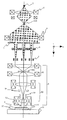
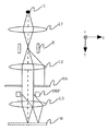
図1は本発明の実施例に係る電子線露光装置の要部構成の概略を示す概略図である。
図1において、電子銃(図示せず)で発生した電子線はクロスオーバ像を形成する。(以下、このクロスオーバ像を電子源1と記す)。
この電子源1から放射される電子ビームは、ビーム整形光学系2を介して、電子源1の像(SI)3を形成する。
As an example of the charged particle beam exposure apparatus, an example of an electron beam exposure apparatus is shown in the embodiment. The present invention is not limited to an electron beam and can be similarly applied to an exposure apparatus using an ion beam.
<Description of components of electron beam exposure apparatus>
FIG. 1 is a schematic view showing an outline of a main configuration of an electron beam exposure apparatus according to an embodiment of the present invention.
In FIG. 1, an electron beam generated by an electron gun (not shown) forms a crossover image. (Hereinafter, this crossover image is referred to as an electron source 1).
The electron beam emitted from the
像(SI)3からの電子ビームは、コリメータレンズ4によって略平行の電子ビームとなる。略平行な電子ビームは複数の開口を有するアパーチャアレイ5を照明する。
アパーチャアレイ5は、複数の開孔を有し、電子ビームを複数の電子ビームに分割する。
アパーチャアレイ5で分割された複数の電子ビームは、静電レンズが複数形成された静電レンズアレイ6により、像(SI)3の中間像を形成する。中間像面には、静電型偏向器であるブランカーが複数形成されたブランカーアレイ7が配置されている。
The electron beam from the image (SI) 3 becomes a substantially parallel electron beam by the
The
The plurality of electron beams divided by the
中間像面の下流には、2段の対称磁気タブレット・レンズ81,82で構成された縮小電子光学系8があり、複数の中間像がウエハ9上に投影される。
このとき、ブランカーアレイ7で偏向された電子ビームは、ブランキングアパーチャBAによって遮断されるため、ウエハ9には照射されない。
一方、ブランカーアレイ7で偏向されない電子ビームは、ブランキングアパーチャBAによって遮断されないため、ウエハ9に照射される。
Downstream of the intermediate image plane, there is a reduction electron
At this time, since the electron beam deflected by the
On the other hand, since the electron beam that is not deflected by the
下段のダブレット・レンズ82内には、複数の電子ビームを同時にX,Y方向の所望の位置に変位させるための偏向器10、及び複数の電子ビームのフォーカスを同時に調整するフォーカスコイル12が配置されている。
XYステージ13はウェハ9を搭載し、光軸と直交するXY方向に移動可能である。
XYステージ13上にはウェハ9を固着するための静電チャック15と電子ビームの形状を測定するための電子ビーム入射側にナイフエッジを有する半導体検出器14が配置されている。
In the lower
The
An
<システム構成及び描画方法の説明>
実施例のシステム構成を図2に示す。図2は、実施例の露光装置のシステム構成を示すブロック図である。
ブランカーアレイ制御回路21は、ブランカーアレイ7を構成する複数のブランカーを個別に制御する。偏向器制御回路22は、偏向器10を制御する。電子ビーム形状検出回路23は、半導体検出器14からの信号を処理する。
フォーカス制御回路24は、フォーカスコイル12の焦点距離を調整することにより縮小電子光学系8の焦点位置を制御する。ステージ駆動制御回路25は、XYステージ13の位置を検出する不図示のレーザ干渉計と共同してXYステージ13を駆動制御する。
主制御系26は、例えばCPUもしくはMPUであり、上記複数の制御回路を制御し、電子線露光装置全体を管理する。
<Description of system configuration and drawing method>
The system configuration of the embodiment is shown in FIG. FIG. 2 is a block diagram showing the system configuration of the exposure apparatus of the embodiment.
The blanker
The
The
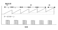
実施例の描画方法(荷電粒子線描画方法)の一例を図3に示す。図3は、実施例の描画方法(荷電粒子線描画方法)の一例を説明する説明図である。
本例の描画方法は、まず複数の電子ビームを偏向させるとともに、ブランカーアレイ制御回路21に命じ、ウエハ9に露光すべきピクセルに応じた指令値に基づいてブランカーアレイ7のブランカーを個別にon/offさせる。
主制御系26は、露光制御データに基づいて、偏向制御回路22に命じ、偏向器10によって、図3に示すようにウエハ9上の対応する要素露光領域(EF)をラスタースキャン露光する(描画ステップ)。
各電子ビームの要素露光領域(EF)は、2次元に隣接するように設定されているので、その結果、同時に露光される複数の要素露光領域(EF)で構成されるサブフィールド(SF)が露光される(描画ステップ−1)。
An example of the drawing method (charged particle beam drawing method) of the embodiment is shown in FIG. FIG. 3 is an explanatory diagram illustrating an example of a drawing method (charged particle beam drawing method) according to the embodiment.
The drawing method of this example first deflects a plurality of electron beams and instructs the blanker
The
Since the element exposure area (EF) of each electron beam is set so as to be adjacent in two dimensions, as a result, a subfield (SF) composed of a plurality of element exposure areas (EF) that are exposed simultaneously is formed. Exposure is performed (drawing step-1).
主制御系26は、サブフィールド(SF1)1を露光後、偏向制御回路22に命じ、偏向器10によって、複数の電子ビームを偏向させ、即ちパターンの描画位置を線幅の測定方向への移動を含め、次のサブフィールド(SF2)2を露光する(描画ステップ−2)。
このとき、偏向によってサブフィールドが変わることにより、各電子ビームが縮小電子光学系8を介して縮小投影される際の収差も変わる。
一方、図4は、各ドーズパターンと露光時間の関係を説明する説明図である。3発目までの各ドーズパターンの露光時間は一様に等しいものとして良いが、4発目のドーズパターンは、0.5ns毎に露光時間が増加する関係にある。
After exposing the subfield (SF1) 1, the
At this time, as the subfield changes due to deflection, the aberration when each electron beam is reduced and projected via the reduction electron
On the other hand, FIG. 4 is an explanatory diagram for explaining the relationship between each dose pattern and the exposure time. Although the exposure time of each dose pattern up to the third shot may be uniformly equal, the fourth dose pattern has a relationship that the exposure time increases every 0.5 ns.
<ドーズ補正量の説明>
ドーズパターンに対する線幅付与量を求めるためのドーズパターンの一例を図5に示す。図5は、各ドーズパターンの実際の線幅を計る際の偏向位置座標とドーズパターンの関係を説明する説明図である。
ドーズパターンは、図5に示すように、偏向位置の移動に同期し、かつ所定のクロックパルスのカウントとともに所定時間の間の露光処理を行うものである。
一方、電子ビームの偏向位置は、偏向器10により制御されるものであり、ドーズパターンはブランカーアレイ7によって制御される。
<Description of dose correction amount>
An example of a dose pattern for determining the line width imparting amount for the dose pattern is shown in FIG. FIG. 5 is an explanatory diagram for explaining the relationship between the deflection position coordinates and the dose pattern when measuring the actual line width of each dose pattern.
As shown in FIG. 5, the dose pattern synchronizes with the movement of the deflection position and performs exposure processing for a predetermined time together with a predetermined clock pulse count.
On the other hand, the deflection position of the electron beam is controlled by the
図6は、ナイフエッジ上のドーズパターンを説明する説明図である。図6の横軸は、指令により形成したい線幅を示し、縦軸は実際の線幅を示す。
電子ビームは、図6に示すように、図5に示す偏向時間t内にナイフエッジ上にドーズパターンに対応した描画パターンを形成する。
そして、例えば主制御系26は、偏向時間内t内に半導体検出器(SSD)に蓄積された電荷粒子量を測定(測定工程)し、順次、次の偏向時間t内の電荷粒子量を測定する(測定ステップ)。
それにより、描画パターンがナイフエッジ上の位置を移動させたときの電荷粒子量を測定することと等価となる。
FIG. 6 is an explanatory diagram for explaining a dose pattern on a knife edge. The horizontal axis in FIG. 6 indicates the line width desired to be formed by the command, and the vertical axis indicates the actual line width.
As shown in FIG. 6, the electron beam forms a drawing pattern corresponding to the dose pattern on the knife edge within the deflection time t shown in FIG.
For example, the
This is equivalent to measuring the amount of charged particles when the drawing pattern is moved on the knife edge.
そのため位置対計測の関係、即ち測定された荷電粒子線量と描画位置とに基づいて電荷粒子量を位置に関して微分することにより、描画パターンのプロファイル及びその線幅を求める。
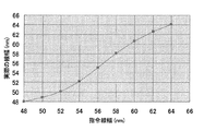
さらに図4に示す他のドーズパターンについても同様の計測を行う。その結果、ドーズパターンに対する実際の線幅の関係が図7に示すように求めることができる。
従って、実際の線幅は、図7に示すように、指令線幅(例えばドーズ指令値)の増加に比例することが分る。
Therefore, the profile of the drawing pattern and its line width are obtained by differentiating the charged particle amount with respect to the position based on the relationship between the position and measurement, that is, the measured charged particle dose and the drawing position.
Further, the same measurement is performed for the other dose patterns shown in FIG. As a result, the relationship between the actual line width and the dose pattern can be obtained as shown in FIG.
Accordingly, it can be seen that the actual line width is proportional to the increase in the command line width (for example, the dose command value), as shown in FIG.
一方、図8は、ドーズ指令値の具体的な補正関係を説明する説明図である。図8の縦軸は設計上のドーズ指令値(指令時間)を示し、横軸は設計上の線幅付与量を与えるドーズ指令値(実行時間)を示す。
ドーズ指令値(指令時間)、及びドーズ指令値(実行時間)の双方は、互いに比例する関係にあることが分る。
そこで、実際の線幅付与量が設計上のものと同一になるように、図8に示す関係を一例として下記のようなドーズ指令値の補正式を求める(補正値決定ステップ)。
D1=f(D0) ・・・(式1)
D0:設計上のドーズ指令値
D1:補正されたドーズ指令値
On the other hand, FIG. 8 is an explanatory diagram illustrating a specific correction relationship of the dose command value. The vertical axis in FIG. 8 indicates the design dose command value (command time), and the horizontal axis indicates the dose command value (execution time) that gives the designed line width provision amount.
It can be seen that both the dose command value (command time) and the dose command value (execution time) are proportional to each other.
Accordingly, the following correction formula for the dose command value is obtained by taking the relationship shown in FIG. 8 as an example so that the actual line width provision amount is the same as the design (correction value determination step).
D1 = f (D0) (Formula 1)
D0: Designed dose command value D1: Corrected dose command value
次に、図9を用いて、ブランカーの指令値の作成方法について説明する。図9は、ブランカーの指令値の作成方法を説明するフローチャートである。
(ステップ1)まずパターンエッジに位置するピクセルのドーズ指令信号が異なる複数のパターンを描画する(描画ステップ)。
(ステップ2)複数のパターンの荷電粒子量の測定に基づいてパターンの線幅を測定する(測定ステップ)。
(ステップ3)前記異なるドーズ指令信号とそれに対応する前記測定ステップの測定結果とに基づいてドーズ指令信号の補正値を決定する(補正値決定ステップ)。
Next, a method of creating a blanker command value will be described with reference to FIG. FIG. 9 is a flowchart for explaining a method of creating a blanker command value.
(Step 1) First, a plurality of patterns having different dose command signals for pixels located at pattern edges are drawn (drawing step).
(Step 2) The line width of the pattern is measured based on the measurement of the amount of charged particles of a plurality of patterns (measurement step).
(Step 3) A correction value of the dose command signal is determined based on the different dose command signals and the corresponding measurement results of the measurement step (correction value determination step).
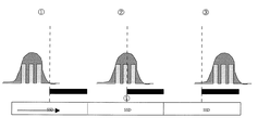
図10は、例えば図4に示すドーズパターンを上記補正方法によって補正した結果の具体例を示す。図10の縦軸は線幅変化を示し、横軸はパターンの移動量を示す。
ドーズパターン(露光時間)は、図10にも示すように、例えばパターンの移動量が増加しても変化量が少ない方が好ましい。
これに対しドーズ指令信号に補正を行わない場合は、図10に示すように、線幅が大きく変化し、補正を行う場合は線幅の変化が少なくなるという結果を得ることができた。
即ち、従来のように補正がない場合は、指令値通りにドーズを与えるべきであるが、実際のドーズはその通りにならないという傾向があった。
しかし、実施例の荷電粒子線描画方法では、上記指令値に沿うドーズを得るように、指令値を上述の如く補正しているので、パターンの移動による線幅変化が小さくなり、パターン形成の信頼性が向上するという明らかな改善が見られた。
FIG. 10 shows a specific example of the result of correcting the dose pattern shown in FIG. 4 by the above correction method, for example. The vertical axis in FIG. 10 indicates the change in line width, and the horizontal axis indicates the amount of movement of the pattern.
As shown in FIG. 10, it is preferable that the dose pattern (exposure time) has a small amount of change even if the amount of movement of the pattern increases, for example.
In contrast, as shown in FIG. 10, when the dose command signal is not corrected, the line width changes greatly, and when the correction is performed, the change in the line width decreases.
That is, when there is no correction as in the prior art, the dose should be given according to the command value, but the actual dose tends not to do so.
However, in the charged particle beam drawing method of the embodiment, since the command value is corrected as described above so as to obtain the dose along the command value, the change in line width due to the movement of the pattern becomes small, and the reliability of pattern formation is reduced. There was a clear improvement in performance.
即ち、実施例の荷電粒子線描画方法においては、荷電粒子線の線幅の測定及び補正を効率的に行うため、所望の微細な描画が容易に可能であり、かつ所望の描画に際してその効率と信頼性を向上させることが可能である。
また、実施例の露光装置(電子線露光装置)においては、その荷電粒子線描画方法を適用するため、所望の露光処理を行うことができ、かつ微細な露光処理に際してその歩留まりを向上させ、露光処理の効率化と信頼性を向上させることが可能である。
That is, in the charged particle beam drawing method of the embodiment, since the measurement and correction of the line width of the charged particle beam is efficiently performed, desired fine drawing can be easily performed, and the efficiency of the desired drawing can be reduced. Reliability can be improved.
Further, in the exposure apparatus (electron beam exposure apparatus) of the embodiment, since the charged particle beam drawing method is applied, a desired exposure process can be performed, and the yield is improved in the fine exposure process. It is possible to improve processing efficiency and reliability.
(デバイス製造方法の実施例)
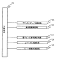
次に上記説明した電子線露光装置を利用したデバイス製造方法の実施例を説明する。図11は微小デバイス(ICやLSI等の半導体チップ、液晶パネル、CCD、薄膜磁気ヘッド、マイクロマシン等)の製造のフローを示す。
まずステップ4(回路設計)では半導体デバイスの回路設計を行なう。ステップ5(露光制御データ作成)では設計した回路パターンに基づいて露光装置の露光制御データを作成する。
一方、ステップ6(ウエハ製造)ではシリコン等の材料を用いてウエハを製造する。
ステップ7(ウエハプロセス)は前工程と呼ばれ、上記用意した露光制御データが入力された露光装置とウエハを用いて、リソグラフィ技術によってウエハ上に実際の回路を形成する。
(Example of device manufacturing method)
Next, an embodiment of a device manufacturing method using the electron beam exposure apparatus described above will be described. FIG. 11 shows a flow of manufacturing a microdevice (a semiconductor chip such as an IC or LSI, a liquid crystal panel, a CCD, a thin film magnetic head, a micromachine, etc.).
First, in step 4 (circuit design), a semiconductor device circuit is designed. In step 5 (exposure control data creation), exposure control data for the exposure apparatus is created based on the designed circuit pattern.
On the other hand, in step 6 (wafer manufacture), a wafer is manufactured using a material such as silicon.
Step 7 (wafer process) is called a pre-process, and an actual circuit is formed on the wafer by lithography using the wafer and the exposure apparatus to which the prepared exposure control data is input.
次のステップ8(組み立て)は後工程と呼ばれ、ステップ7によって作製されたウエハを用いて半導体チップ化する工程であり、アッセンブリ工程(ダイシング、ボンディング)、パッケージング工程(チップ封入)等の工程を含む。
ステップ9(検査)ではステップ8で作製された半導体デバイスの動作確認テスト、耐久性テスト等の検査を行なう。
こうした工程を経て半導体デバイスが完成し、これが出荷(ステップ10)される。
The next step 8 (assembly) is called a post-process, which is a process for forming a semiconductor chip using the wafer produced in
In step 9 (inspection), the semiconductor device manufactured in
Through these steps, the semiconductor device is completed and shipped (step 10).
図12は上記ウエハプロセス(ステップ7)の詳細なフローを示す。ステップ11(酸化)ではウエハの表面を酸化させる。ステップ12(CVD)ではウエハ表面に絶縁膜を形成する。
ステップ13(電極形成)ではウエハ上に電極を蒸着によって形成する。ステップ14(イオン打込み)ではウエハにイオンを打ち込む。ステップ15(レジスト処理)ではウエハに感光剤を塗布する。
ステップ16(露光)では上記説明した露光装置によって回路パターンをウエハに焼付露光する。ステップ17(現像)では露光したウエハを現像する。ステップ18(エッチング)では現像したレジスト像以外の部分を削り取る。
ステップ19(レジス剥離)ではエッチングが済んで不要となったレジストを取り除く。これらのステップを繰り返し行なうことによって、ウエハ上に多重に回路パターンが形成される。
以上の結果から、実施例のデバイス製造方法においては、上述の電子線露光装置を適用するため、製造の歩留まりが向上し、かつ微細加工の効率化と信頼性を高めることが可能となった。
FIG. 12 shows a detailed flow of the wafer process (step 7). In step 11 (oxidation), the wafer surface is oxidized. In step 12 (CVD), an insulating film is formed on the wafer surface.
In step 13 (electrode formation), an electrode is formed on the wafer by vapor deposition. In step 14 (ion implantation), ions are implanted into the wafer. In step 15 (resist process), a photosensitive agent is applied to the wafer.
In step 16 (exposure), the circuit pattern is printed onto the wafer by exposure using the exposure apparatus described above. In step 17 (development), the exposed wafer is developed. In step 18 (etching), portions other than the developed resist image are removed.
In step 19 (resist stripping), the resist that has become unnecessary after the etching is removed. By repeating these steps, multiple circuit patterns are formed on the wafer.
From the above results, in the device manufacturing method of the example, since the above-described electron beam exposure apparatus was applied, the manufacturing yield was improved, and the efficiency and reliability of microfabrication could be improved.
1 電子源
2 ビーム整形光学系
3 光源像
4 コリメータレンズ
5 アパーチャアレイ
6 静電レンズ・アレイ
7 ブランカーアレイ
8 縮小電子光学系
9 ウェハ
10 偏向器
12 フォーカスコイル
13 XYステージ
14 半導体検出器
15 静電チャック
DESCRIPTION OF
Claims (4)
前記パターンのエッジに位置する前記複数のピクセルのドーズ指令信号が異なる前記複数のパターンを描画する描画ステップと、
前記複数のパターンの線幅を測定する測定ステップと、
前記異なるドーズ指令信号と前記異なるドーズ指令信号に対応する前記測定ステップの測定結果とに基づいて前記ドーズ指令信号の補正値を決定する補正値決定ステップとを有することを特徴とする荷電粒子線描画方法。 In a charged particle beam drawing method for exposing a pattern composed of a plurality of pixels on a substrate by raster scanning a charged particle beam,
A drawing step of drawing the plurality of patterns in which dose command signals of the plurality of pixels located at edges of the pattern are different;
A measuring step for measuring line widths of the plurality of patterns;
Charged particle beam drawing comprising: a correction value determining step for determining a correction value of the dose command signal based on the different dose command signal and a measurement result of the measurement step corresponding to the different dose command signal Method.
前記ウエハを現像する工程とを備えることを特徴とするデバイス製造方法。 Exposing the wafer using the exposure apparatus according to claim 3;
And a step of developing the wafer.
Priority Applications (2)
| Application Number | Priority Date | Filing Date | Title |
|---|---|---|---|
| JP2006169797A JP2008004596A (en) | 2006-06-20 | 2006-06-20 | Charged particle beam drawing method, aligner, and process for fabricating device |
| US11/762,180 US8692218B2 (en) | 2006-06-20 | 2007-06-13 | Charged particle beam exposure apparatus |
Applications Claiming Priority (1)
| Application Number | Priority Date | Filing Date | Title |
|---|---|---|---|
| JP2006169797A JP2008004596A (en) | 2006-06-20 | 2006-06-20 | Charged particle beam drawing method, aligner, and process for fabricating device |
Publications (2)
| Publication Number | Publication Date |
|---|---|
| JP2008004596A true JP2008004596A (en) | 2008-01-10 |
| JP2008004596A5 JP2008004596A5 (en) | 2009-08-06 |
Family
ID=39008771
Family Applications (1)
| Application Number | Title | Priority Date | Filing Date |
|---|---|---|---|
| JP2006169797A Pending JP2008004596A (en) | 2006-06-20 | 2006-06-20 | Charged particle beam drawing method, aligner, and process for fabricating device |
Country Status (2)
| Country | Link |
|---|---|
| US (1) | US8692218B2 (en) |
| JP (1) | JP2008004596A (en) |
Cited By (4)
| Publication number | Priority date | Publication date | Assignee | Title |
|---|---|---|---|---|
| JP2008004597A (en) * | 2006-06-20 | 2008-01-10 | Canon Inc | Charged particle beam drawing method, aligner, and process for fabricating device |
| JP2013165121A (en) * | 2012-02-09 | 2013-08-22 | Canon Inc | Drawing device, generating method, program and method for manufacturing article |
| JP2015029045A (en) * | 2013-06-26 | 2015-02-12 | キヤノン株式会社 | Drawing device, and manufacturing method of article |
| JP2021044352A (en) * | 2019-09-10 | 2021-03-18 | 株式会社ニューフレアテクノロジー | Multi-charged particle beam evaluation method and multi-charged particle beam drawing device |
Families Citing this family (1)
| Publication number | Priority date | Publication date | Assignee | Title |
|---|---|---|---|---|
| JP5859778B2 (en) * | 2011-09-01 | 2016-02-16 | 株式会社ニューフレアテクノロジー | Multi-charged particle beam writing apparatus and multi-charged particle beam writing method |
Citations (8)
| Publication number | Priority date | Publication date | Assignee | Title |
|---|---|---|---|---|
| JPH0391228A (en) * | 1989-09-01 | 1991-04-16 | Jeol Ltd | Measuring method of diameter of charged particle beam |
| JPH04116915A (en) * | 1990-09-07 | 1992-04-17 | Jeol Ltd | Drawing-beam diameter adjusting method |
| JP2001168018A (en) * | 1999-12-13 | 2001-06-22 | Canon Inc | Device and method for exposing charged corpuscular beam, determining method for exposure correction data and method for producing device by applying the same method |
| JP2004040010A (en) * | 2002-07-08 | 2004-02-05 | Renesas Technology Corp | Pattern drawing method |
| JP2004193516A (en) * | 2002-12-13 | 2004-07-08 | Canon Inc | Charged-particle beam exposure apparatus, and control method thereof |
| JP2005032838A (en) * | 2003-07-08 | 2005-02-03 | Canon Inc | Method and device for charged particle beam lithography and method of manufacturing device |
| JP2006019439A (en) * | 2004-06-30 | 2006-01-19 | Canon Inc | Charged particle beam exposure apparatus, method for exposing charged beam and method for manufacturing device |
| JP2006019437A (en) * | 2004-06-30 | 2006-01-19 | Canon Inc | Charged particle beam exposure method, charged particle beam exposure apparatus, and device manufacturing method |
Family Cites Families (16)
| Publication number | Priority date | Publication date | Assignee | Title |
|---|---|---|---|---|
| JPH0639155B2 (en) * | 1986-02-21 | 1994-05-25 | 名幸電子工業株式会社 | Method for manufacturing copper clad laminate |
| JP3274212B2 (en) * | 1993-03-18 | 2002-04-15 | 株式会社日立製作所 | Electron beam detector and electron beam drawing apparatus using the same |
| US5432352A (en) * | 1993-09-20 | 1995-07-11 | Eaton Corporation | Ion beam scan control |
| JP3469422B2 (en) * | 1996-02-23 | 2003-11-25 | 株式会社東芝 | Charged beam writing method and writing apparatus |
| US5834783A (en) * | 1996-03-04 | 1998-11-10 | Canon Kabushiki Kaisha | Electron beam exposure apparatus and method, and device manufacturing method |
| US5981961A (en) * | 1996-03-15 | 1999-11-09 | Applied Materials, Inc. | Apparatus and method for improved scanning efficiency in an ion implanter |
| AU4167199A (en) * | 1998-06-17 | 2000-01-05 | Nikon Corporation | Method for producing mask |
| JP4410871B2 (en) * | 1999-03-25 | 2010-02-03 | キヤノン株式会社 | Charged particle beam exposure apparatus and device manufacturing method using the apparatus |
| EP1339100A1 (en) * | 2000-12-01 | 2003-08-27 | Ebara Corporation | Inspection method and apparatus using electron beam, and device production method using it |
| EP1249734B1 (en) * | 2001-04-11 | 2012-04-18 | Fujitsu Semiconductor Limited | Rectangle/lattice data conversion method for charged particle beam exposure mask pattern and charged particle beam exposure method |
| US7282427B1 (en) * | 2006-05-04 | 2007-10-16 | Applied Materials, Inc. | Method of implanting a substrate and an ion implanter for performing the method |
| JP2004228430A (en) * | 2003-01-24 | 2004-08-12 | Tokyo Seimitsu Co Ltd | Method and device for adjusting electron beam proximity exposure device |
| US7005659B2 (en) * | 2003-07-08 | 2006-02-28 | Canon Kabushiki Kaisha | Charged particle beam exposure apparatus, charged particle beam exposure method, and device manufacturing method using the same apparatus |
| US7462848B2 (en) * | 2003-10-07 | 2008-12-09 | Multibeam Systems, Inc. | Optics for generation of high current density patterned charged particle beams |
| US6870170B1 (en) * | 2004-03-04 | 2005-03-22 | Applied Materials, Inc. | Ion implant dose control |
| JP2006079911A (en) * | 2004-09-09 | 2006-03-23 | Hitachi High-Technologies Corp | Electron beam current measuring method, electron beam drawing apparatus, and electron beam detector |
-
2006
- 2006-06-20 JP JP2006169797A patent/JP2008004596A/en active Pending
-
2007
- 2007-06-13 US US11/762,180 patent/US8692218B2/en not_active Expired - Fee Related
Patent Citations (8)
| Publication number | Priority date | Publication date | Assignee | Title |
|---|---|---|---|---|
| JPH0391228A (en) * | 1989-09-01 | 1991-04-16 | Jeol Ltd | Measuring method of diameter of charged particle beam |
| JPH04116915A (en) * | 1990-09-07 | 1992-04-17 | Jeol Ltd | Drawing-beam diameter adjusting method |
| JP2001168018A (en) * | 1999-12-13 | 2001-06-22 | Canon Inc | Device and method for exposing charged corpuscular beam, determining method for exposure correction data and method for producing device by applying the same method |
| JP2004040010A (en) * | 2002-07-08 | 2004-02-05 | Renesas Technology Corp | Pattern drawing method |
| JP2004193516A (en) * | 2002-12-13 | 2004-07-08 | Canon Inc | Charged-particle beam exposure apparatus, and control method thereof |
| JP2005032838A (en) * | 2003-07-08 | 2005-02-03 | Canon Inc | Method and device for charged particle beam lithography and method of manufacturing device |
| JP2006019439A (en) * | 2004-06-30 | 2006-01-19 | Canon Inc | Charged particle beam exposure apparatus, method for exposing charged beam and method for manufacturing device |
| JP2006019437A (en) * | 2004-06-30 | 2006-01-19 | Canon Inc | Charged particle beam exposure method, charged particle beam exposure apparatus, and device manufacturing method |
Cited By (7)
| Publication number | Priority date | Publication date | Assignee | Title |
|---|---|---|---|---|
| JP2008004597A (en) * | 2006-06-20 | 2008-01-10 | Canon Inc | Charged particle beam drawing method, aligner, and process for fabricating device |
| JP2013165121A (en) * | 2012-02-09 | 2013-08-22 | Canon Inc | Drawing device, generating method, program and method for manufacturing article |
| JP2015029045A (en) * | 2013-06-26 | 2015-02-12 | キヤノン株式会社 | Drawing device, and manufacturing method of article |
| JP2021044352A (en) * | 2019-09-10 | 2021-03-18 | 株式会社ニューフレアテクノロジー | Multi-charged particle beam evaluation method and multi-charged particle beam drawing device |
| CN112558420A (en) * | 2019-09-10 | 2021-03-26 | 纽富来科技股份有限公司 | Method for evaluating multiple charged particle beams and multiple charged particle beam drawing device |
| JP7310466B2 (en) | 2019-09-10 | 2023-07-19 | 株式会社ニューフレアテクノロジー | Multi-charged particle beam evaluation method |
| CN112558420B (en) * | 2019-09-10 | 2024-03-15 | 纽富来科技股份有限公司 | Multi-charged particle beam evaluation method and multi-charged particle beam drawing device |
Also Published As
| Publication number | Publication date |
|---|---|
| US20080067402A1 (en) | 2008-03-20 |
| US8692218B2 (en) | 2014-04-08 |
Similar Documents
| Publication | Publication Date | Title |
|---|---|---|
| JP5116996B2 (en) | Charged particle beam drawing method, exposure apparatus, and device manufacturing method | |
| JP4870437B2 (en) | Method for calculating deflection aberration correction voltage and charged particle beam writing method | |
| US20020005494A1 (en) | Charged-particle-beam microlithography apparatus and methods including proximity-effect correction | |
| JP2007115999A (en) | Process and device for charged particle beam exposure employing character projection (cp) method, and program | |
| JP2006261342A (en) | Charged particle exposure apparatus and device manufacturing method | |
| JP4603305B2 (en) | Exposure method, pattern dimension adjustment method, and focal blur amount acquisition method | |
| JP2004273526A (en) | Reticle manufacturing method, reticle, and charged particle beam exposure method | |
| JP2008004596A (en) | Charged particle beam drawing method, aligner, and process for fabricating device | |
| JP2017022359A (en) | Adjustment method for charged particle beam lithography apparatus, and charged particle beam lithography method | |
| JP2005032837A (en) | Method for charged particle beam lithography and method of manufacturing device using the same | |
| US7005659B2 (en) | Charged particle beam exposure apparatus, charged particle beam exposure method, and device manufacturing method using the same apparatus | |
| JP4468752B2 (en) | Charged particle beam exposure method, charged particle beam exposure apparatus and device manufacturing method | |
| US7394068B2 (en) | Mask inspection apparatus, mask inspection method, and electron beam exposure system | |
| JP2006210455A (en) | Charged particle exposure apparatus and method of fabricating device using apparatus | |
| JP2001244165A (en) | Method for correcting proximity effect, reticle, and method of manufacturing device | |
| JP4804136B2 (en) | Charged particle beam apparatus and device manufacturing method | |
| JP4402529B2 (en) | Charged particle beam exposure method, charged particle beam exposure apparatus and device manufacturing method | |
| JP2006019439A (en) | Charged particle beam exposure apparatus, method for exposing charged beam and method for manufacturing device | |
| JP2003077798A (en) | Proximity effect correcting method and device manufacturing method | |
| JP4494734B2 (en) | Charged particle beam drawing method, charged particle beam exposure apparatus, and device manufacturing method | |
| JP2008311311A (en) | Charged particle beam exposure method and charged particle beam exposure system | |
| JP4356064B2 (en) | Charged particle beam exposure apparatus and device manufacturing method using the apparatus | |
| JP2006210459A (en) | Charged particle beam exposure apparatus and method, and method of fabricating device | |
| JP2000323376A (en) | Electron beam transfer exposure method and device manufacture using the same | |
| JP2001237175A (en) | Proximity effect correction method, reticle, and method of manufacturing device |
Legal Events
| Date | Code | Title | Description |
|---|---|---|---|
| RD03 | Notification of appointment of power of attorney |
Free format text: JAPANESE INTERMEDIATE CODE: A7423 Effective date: 20090413 |
|
| A521 | Request for written amendment filed |
Free format text: JAPANESE INTERMEDIATE CODE: A523 Effective date: 20090619 |
|
| A621 | Written request for application examination |
Free format text: JAPANESE INTERMEDIATE CODE: A621 Effective date: 20090619 |
|
| RD03 | Notification of appointment of power of attorney |
Free format text: JAPANESE INTERMEDIATE CODE: A7423 Effective date: 20090709 |
|
| A977 | Report on retrieval |
Free format text: JAPANESE INTERMEDIATE CODE: A971007 Effective date: 20111013 |
|
| A131 | Notification of reasons for refusal |
Free format text: JAPANESE INTERMEDIATE CODE: A131 Effective date: 20111021 |
|
| A521 | Request for written amendment filed |
Free format text: JAPANESE INTERMEDIATE CODE: A523 Effective date: 20111219 |
|
| A02 | Decision of refusal |
Free format text: JAPANESE INTERMEDIATE CODE: A02 Effective date: 20120406 |