JP4468752B2 - Charged particle beam exposure method, charged particle beam exposure apparatus and device manufacturing method - Google Patents
Charged particle beam exposure method, charged particle beam exposure apparatus and device manufacturing method Download PDFInfo
- Publication number
- JP4468752B2 JP4468752B2 JP2004194769A JP2004194769A JP4468752B2 JP 4468752 B2 JP4468752 B2 JP 4468752B2 JP 2004194769 A JP2004194769 A JP 2004194769A JP 2004194769 A JP2004194769 A JP 2004194769A JP 4468752 B2 JP4468752 B2 JP 4468752B2
- Authority
- JP
- Japan
- Prior art keywords
- exposure
- charged particle
- area
- pattern
- particle beam
- Prior art date
- Legal status (The legal status is an assumption and is not a legal conclusion. Google has not performed a legal analysis and makes no representation as to the accuracy of the status listed.)
- Expired - Fee Related
Links
Images


Description
本発明は、主に半導体集積回路等の露光に用いられる電子線露光装置、イオンビーム露光装置等に適した荷電粒子線露光(描画)方法に関するものである。 The present invention relates to a charged particle beam exposure (drawing) method suitable for an electron beam exposure apparatus, an ion beam exposure apparatus and the like mainly used for exposure of a semiconductor integrated circuit or the like.
荷電粒子線露光装置には、ビームをスポット状にして使用するポイントビーム型、サイズ可変の矩形断面にして使用する可変矩形ビーム型、及びステンシルを使用して所望断面形状にするステンシルマスク型等の装置がある。 The charged particle beam exposure apparatus includes a point beam type which uses a beam in a spot shape, a variable rectangular beam type which uses a variable size rectangular cross section, and a stencil mask type which uses a stencil to obtain a desired cross sectional shape. There is a device.
ポイントビーム型の電子ビーム露光装置では、スループットが低いので、研究開発用にしか使用されていない。可変矩形ビーム型の電子ビーム露光装置では、ポイント型と比べるとスループットが1〜2桁高いが、0.1μm程度の微細なパターンが高集積度で詰まったパターンを露光する場合などでは、やはりスループットの点で問題が多い。他方、ステンシルマスク型の電子ビーム露光装置は、可変矩形アパーチャに相当する部分に複数の繰り返しパターン透過孔を形成したステンシルマスクを用いる。従って、ステンシルマスク型の電子ビーム露光装置では、繰り返しパターンを露光する場合のメリットが大きいが、1枚のステンシルマスクに納まらない多数の転写パターンが必要な半導体回路に対しては、複数牧のステンシルマスクを作成しておいて、それを1枚ずつ取り出して使用する必要があり、マスク交換の時間が必要になるため、著しくスループットが低下するという問題点がある。 Since the point beam type electron beam exposure apparatus has a low throughput, it is used only for research and development. In the variable rectangular beam type electron beam exposure apparatus, the throughput is one to two orders of magnitude higher than that of the point type. However, in the case of exposing a pattern in which a fine pattern of about 0.1 μm is packed with a high degree of integration, the throughput is still the same. There are many problems. On the other hand, a stencil mask type electron beam exposure apparatus uses a stencil mask in which a plurality of repetitive pattern transmission holes are formed in a portion corresponding to a variable rectangular aperture. Therefore, the electron beam exposure apparatus of the stencil mask type has a great advantage when exposing repeated patterns, but for semiconductor circuits that require a large number of transfer patterns that do not fit in one stencil mask, a plurality of stencil masks are used. Since it is necessary to prepare the masks one by one and use them one after another, and it takes time to replace the masks, there is a problem that the throughput is significantly reduced.
この問題点を解決する装置として、複数の電子ビームを設計上の座標に沿って試料面に照射し、設計上の座標に沿ってその複数の電子ビームを偏向させて試料面を走査させるとともに、描画するパターンに応じて複数の電子ビームを個別にon/offしてパターンを描画するマルチ電子ビーム型露光装置がある。マルチ電子ビーム型露光装置は、ステンシルマスクを用いずに任意の描画パターンを描画できるのでスループットがより改善できるという特徴がある。 As a device to solve this problem, the sample surface is irradiated with a plurality of electron beams along the design coordinates, and the sample surface is scanned along with the deflection of the plurality of electron beams along the design coordinates, There is a multi-electron beam exposure apparatus that draws a pattern by individually turning on / off a plurality of electron beams according to the pattern to be drawn. The multi-electron beam exposure apparatus has a feature that throughput can be further improved because an arbitrary drawing pattern can be drawn without using a stencil mask.
図5(A)に、従来のマルチ電子ビーム型露光装置の概要を示す。501a,501b,501cは、個別に電子ビームをon/offできる電子銃である。502は、電子銃501a,501b,501cからの複数の電子ビームをウエハ503上に縮小投影する縮小電子光学系であり、504は、ウエハ503に縮小投影された複数の電子ビームを偏向させる偏向器である。
FIG. 5A shows an outline of a conventional multi-electron beam exposure apparatus.
図5(B)に示すように、電子銃501a,501b,501cからの電子ビームB1,B2,B3は、偏向器504によって同一の偏向量を与えられる。それにより、それぞれのビーム基準位置を基準として、各電子ビームは偏向器504が定める配列(要素露光領域)に従ってウエハ上での位置を順次整定して移動する。すなわち、同一の配列に従って露光すべきパターンを露光する様子を示している。各電子ビームは、同時刻の配列上の位置を(1,1)、(1,2)、....(1,16)、(2,1)、(2,2)、....(2,16)、(3,1)、..となるように位置を整定して移動していく。ここで、それぞれの電子ビームの小露光領域ES1,ES2,ES3は、偏向器504によって定まり、各要素露光領域は隣接される。そして、各小露光領域では、電子ビームを偏向するとともに電子ビームの照射を制御することによって露光すべきパターン(Pl,P2,P3)が露光される。
各電子ビームB1,B2,B3が露光するパターンP1,P2,P3によって図5(B)のような連続するパターンPOを露光しようとする場合がある。しかしながら、偏向器504の偏向精度もしくは縮小電子光学系502の経時変化等により、図5(C)のように各小露光領域ES1,ES2,ES3が隣接せず、互いに離れることがある。その結果、連続するべきパターンPOは、互いに接しないP1,P2,P3に分断されて、露光される。よって、このようなパターンが露光されたウエハから製造された半導体素子においては、配線の断線等により所望の動作を達成できず、半導体素子製造の歩留まりを著しく低下させるという問題点がある。
Each electron beam B1, B2, B3 is sometimes intended to be exposed to continuous pattern P O as shown in FIG. 5 (B) by the pattern P 1, P 2, P 3 to be exposed. However, depending on the deflection accuracy of the
本発明は、繋ぎを確実に行うことができ、所望パターンを的確に露光することができる荷電粒子線描画方法を提供することを主な目的とする。 The main object of the present invention is to provide a charged particle beam drawing method capable of surely connecting and exposing a desired pattern accurately.
上記目的を達成するための、本発明の荷電粒子線露光方法は、複数の荷電粒子線を基板上の異なる位置に入射させ、前記複数の荷電粒子線を偏向する偏向器によって定められる各荷電粒子線の要素露光領域内で荷電粒子線を偏向させるとともに、各荷電粒子線の前記基板上への照射を制御することで、前記基板上の複数の要素露光領域内にパターンを露光する荷電粒子線露光方法であって、前記複数の要素露光領域のうち隣接する第1要素露光領域と第2要素露光領域とを重複させて多重露光領域を設定する工程と、前記多重露光領域のみに存在するパターン、及び、前記多重露光領域と前記第1要素露光領域又は前記第2要素露光領域における前記多重露光領域以外の領域とにまたがって存在するパターンは多重露光せず、前記多重露光領域と前記第1要素露光領域及び前記第2要素露光領域における前記多重露光領域以外の領域とにまたがって存在するパターンは多重露光する工程と、を有することを特徴とする。 In order to achieve the above object, the charged particle beam exposure method of the present invention includes a plurality of charged particle beams incident on different positions on a substrate, and each charged particle defined by a deflector that deflects the plurality of charged particle beams. A charged particle beam that exposes a pattern in a plurality of element exposure regions on the substrate by deflecting the charged particle beam in the element exposure region of the line and controlling irradiation of each charged particle beam onto the substrate An exposure method comprising: setting a multiple exposure area by overlapping adjacent first element exposure areas and second element exposure areas among the plurality of element exposure areas; and a pattern existing only in the multiple exposure areas and, the multiple patterns existing across the region other than the multiple exposure region exposed region and in the first element exposed region or the second element exposure regions without multiple exposure, the multiple exposure territory The pattern present across the region other than the multiple exposure region in the first element exposure region and the second element exposure region and is characterized by having a step of multiple exposure, the.
以上説明したように、本発明によれば、ラスタースキャン荷電粒子線露光装置において、繋ぎが確実に行え、所望のパターンを露光できる荷電粒子線露光方法を提供することができる。また、この方法を用いてデバイスを製造すれば、従来以上に歩留まりの高いデバイスを製造することができる。 As described above, according to the present invention, it is possible to provide a charged particle beam exposure method capable of reliably connecting and exposing a desired pattern in a raster scan charged particle beam exposure apparatus. Moreover, if a device is manufactured using this method, a device having a higher yield than the conventional device can be manufactured.
荷電粒子線露光装置の一例として本発明の実施例では電子線露光装置を示す。なお、本発明は電子線に限らずイオンビームを用いた露光装置にも同様に適用できる。 As an example of the charged particle beam exposure apparatus, an embodiment of the present invention shows an electron beam exposure apparatus. The present invention is not limited to an electron beam and can be similarly applied to an exposure apparatus using an ion beam.
<電子ビーム露光装置の構成要素の説明>
図1は本発明の実施例1に係る電子線露光装置の要部概略図である。
図1において、電子銃(図示せず)で発生した電子線はクロスオーバ像を形成する(以下、このクロスオーバ像を電子源1と記す)。
<Description of components of electron beam exposure apparatus>
FIG. 1 is a schematic view of the essential portions of an electron beam exposure apparatus according to Embodiment 1 of the present invention.
In FIG. 1, an electron beam generated by an electron gun (not shown) forms a crossover image (hereinafter, this crossover image is referred to as an electron source 1).
この電子源1から放射される電子ビームは、ビーム整形光学系2を介して、電子源1の像3(SI)を形成する。像SIからの電子ビームは、コリメータレンズ4によって略平行の電子ビームとなる。略平行な電子ビームは複数の開口を有するアパチャ−アレイ5を照明する。 The electron beam emitted from the electron source 1 forms an image 3 (SI) of the electron source 1 via the beam shaping optical system 2. The electron beam from the image SI becomes a substantially parallel electron beam by the collimator lens 4. The substantially parallel electron beam illuminates the aperture array 5 having a plurality of apertures.
アパーチャアレイ5は、複数の開口を有し、電子ビームを複数の電子ビームに分割する。アパーチャアレイ5で分割された複数の電子ビームは、静電レンズが複数形成された静電レンズアレイ6により、像SIの中間像を形成する。中間像面には、静電型偏向器であるブランカーが複数形成されたブランカーアレイ7が配置されている。
The aperture array 5 has a plurality of openings and divides the electron beam into a plurality of electron beams. The plurality of electron beams divided by the aperture array 5 forms an intermediate image of the image SI by the electrostatic lens array 6 in which a plurality of electrostatic lenses are formed. A
中間像面の下流には、2段の対称磁気タブレット・レンズ81,82で構成された縮小電子光学系8があり、複数の中間像がウエハ9上に投影される。このとき、ブランカーアレイ7で偏向された電子ビームは、ブランキングアパーチャBAによって遮断されるため、ウエハ9には照射されない。一方、ブランカーアレイ7で偏向されない電子ビームは、ブランキングアパーチャBAによって遮断されないため、ウエハ9に照射される。
Downstream of the intermediate image plane, there is a reduction electron
下段のダブレット・レンズ82内には、複数の電子ビームを同時にX,Y方向の所望の位置に変位させるための偏向器10、及び複数の電子ビームのフォーカスを同時に調整するフォーカスコイル12が配置されている。13はウエハ9を搭載し、光軸と直交するXY方向に移動可能なXYステージである。ステージ13上にはウエハ9を固着するための静電チャック15と電子ビームの形状を測定するための電子ビーム入射側にナイフエッジを有する半導体検出器14が配置されている。
In the lower
<システム構成及び露光方法の説明>
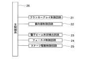
本実施例に係るシステム構成図を図2に示す。ブランカーアレイ制御回路21は、ブランカーアレイ7を構成する複数のブランカーを個別に制御する回路であり、偏向器制御回路22は、偏向器10を制御する回路である。電子ビーム形状検出回路23は、半導体検出器14からの信号を処理する回路であり、フォーカス制御回路24は、フォーカスコイル12の焦点距離を調整することにより縮小電子光学系8の焦点位置を制御する回路であり、ステージ駆動制御回路25は、ステージ13の位置を検出する不図示のレーザ干渉計と共同してステージ13を駆動制御する制御回路である。主制御系26は、上記複数の制御回路を制御し、電子ビーム露光装置全体を管理する。
<Description of system configuration and exposure method>
A system configuration diagram according to the present embodiment is shown in FIG. The blanker
本実施例に係る露光方法の説明図を図3に示す。図3にはニ点鎖線で表した円内の部分拡大図が含まれでいる。 主制御系26は、露光制御データに基づいて、偏向制御回路22に命じ、偏向器10によって、複数の電子ビームを偏向させるとともに、ブランカーアレイ制御回路21に命じ、ウエハ9に露光すべきピクセルPXに応じた指令値に基づいてブランカーアレイ7のブランカーを個別にon/offさせる。各電子ビームは、図3に示すように、ウエハ9上の対応する要素露光領域(EF)をラスタースキャン露光する。各電子ビームEBの要素露光領域(EF)は、2次元に隣接するように設定されているので、その結果、同時に露光される複数の要素露光領域(EF)で構成されるサブフィールド(SF)が露光される。
FIG. 3 shows an explanatory view of the exposure method according to the present embodiment. FIG. 3 includes a partially enlarged view in a circle represented by a two-dot chain line. The
主制御系26は、サブフィールド(SF1)を露光後、次のサブフィールド(SF2)
を露光する為に、偏向制御回路22に命じ、偏向器10によって、複数の電子ビームを偏向させる。
The
In order to perform exposure, the
本実施例に係る描画方法では、図4において、隣接する実線で表した要素露光領域1と点線で表した要素露光領域2とは重複させ、隣接の要素露光領域1及び要素露光領域2の双方で描画(露光)する多重描画領域(多重露光領域)を設定している。そして、要素露光領域1内の実線で表した部分は要素露光領域1で描画し、要素露光領域2内の点線で表した部分は要素露光領域2で描画し、破線で表した部分は要素露光領域1及び要素露光領域2で描画し、かつ多重描画領域では多重描画を行う。 In the drawing method according to this embodiment, in FIG. 4, the element exposure area 1 represented by the solid line adjacent to the element exposure area 2 represented by the dotted line is overlapped, and both the element exposure area 1 and the element exposure area 2 adjacent to each other are overlapped. A multiple drawing area (multiple exposure area) for drawing (exposure) is set. The part represented by the solid line in the element exposure area 1 is drawn in the element exposure area 1, the part represented by the dotted line in the element exposure area 2 is drawn in the element exposure area 2, and the part represented by the broken line is element exposure. Drawing is performed in the region 1 and the element exposure region 2, and multiple drawing is performed in the multiple drawing region.
そのため、たとえ要素露光領域同士の相対的位置関係が設計上の関係から多少ずれても、その形状が歪むだけで、連続パターンは連続パターンとして露光できる。また、多重描画領域の幅は、描画するパターンの中でその線幅の一様性が厳しい例えばゲートのようなパターンを注目パターンとして設定する。そして、その長辺をLとした時、多重描画領域の幅をL以上、すなわち長辺以上に設定している。その結果、多重描画領域に位置する注目パターンは、どちらか一方の要素領域のみで存在するので、繋ぎなしのパターンとして露光できる。 Therefore, even if the relative positional relationship between the element exposure regions is slightly deviated from the design relationship, the continuous pattern can be exposed as a continuous pattern only by distorting the shape. In addition, the width of the multiple drawing area is set as a pattern of interest, for example, a pattern such as a gate whose line width is strict in the pattern to be drawn. When the long side is L, the width of the multiple drawing region is set to L or more, that is, the long side or more . As a result, the target pattern located in the multiple drawing area exists only in one of the element areas, so that it can be exposed as a pattern without connection.
(デバイスの製造方法)
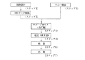
次に上記説明した電子線露光装置を利用したデバイスの製造方法の例を実施例2として説明する。 図6は微小デバイス(ICやLSI等の半導体チップ、液晶パネル、CCD、薄膜磁気ヘッド、マイクロマシン等)の製造のフローを示す。ステップ1(回路設計)では半導体デバイスの回路設計を行なう。ステップ2(EBデータ変換)では設計した回路パターンに基づいて露光装置の露光制御データを作成する。一方、ステップ3(ウエハ製造)ではシリコン等の材料を用いてウエハを製造する。ステップ4(ウエハプロセス)は前工程と呼ばれ、上記用意した露光制御データが入力された露光装置とウエハを用いて、リソグラフィ技術によってウエハ上に実際の回路を形成する。次のステップ5(組み立て)は後工程と呼ばれ、ステップ4によって作製されたウエハを用いて半導体チップ化する工程であり、アッセンブリ工程(ダイシング、ボンディング)、パッケージング工程(チップ封入)等の工程を含む。ステップ6(検査)ではステップ5で作製された半導体デバイスの動作確認テスト、耐久性テスト等の検査を行なう。こうした工程を経て半導体デバイスが完成し、これが出荷(ステップ7)される。
(Device manufacturing method)
Next, an example of a device manufacturing method using the electron beam exposure apparatus described above will be described as a second embodiment. FIG. 6 shows a manufacturing flow of a microdevice (a semiconductor chip such as an IC or LSI, a liquid crystal panel, a CCD, a thin film magnetic head, a micromachine, etc.). In step 1 (circuit design), a semiconductor device circuit is designed. In step 2 (EB data conversion), exposure control data for the exposure apparatus is created based on the designed circuit pattern. On the other hand, in step 3 (wafer manufacture), a wafer is manufactured using a material such as silicon. Step 4 (wafer process) is called a pre-process, and an actual circuit is formed on the wafer by lithography using the wafer and the exposure apparatus to which the prepared exposure control data is input. The next step 5 (assembly) is referred to as a post-process, and is a process for forming a semiconductor chip using the wafer produced in step 4, such as an assembly process (dicing, bonding), a packaging process (chip encapsulation), and the like. including. In step 6 (inspection), inspections such as an operation confirmation test and a durability test of the semiconductor device manufactured in step 5 are performed. Through these steps, the semiconductor device is completed and shipped (step 7).
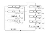
図7は上記ウエハプロセスの詳細なフローを示す。ステップ11(酸化)ではウエハの表面を酸化させる。ステップ12(CVD)ではウエハ表面に絶縁膜を形成する。ステップ13(電極形成)ではウエハ上に電極を蒸着によって形成する。ステップ14(イオン打込み)ではウエハにイオンを打ち込む。ステップ15(レジスト処理)ではウエハに感光剤を塗布する。ステップ16(露光)では上記説明した露光装置によって回路パターンをウエハに焼付露光する。ステップ17(現像)では露光したウエハを現像する。ステップ18(エッチング)では現像したレジスト像以外の部分を削り取る。ステップ19(レジスト剥離)ではエッチングが済んで不要となったレジストを取り除く。これらのステップを繰り返し行なうことによって、ウエハ上に多重に回路パターンが形成される。 FIG. 7 shows a detailed flow of the wafer process. In step 11 (oxidation), the wafer surface is oxidized. In step 12 (CVD), an insulating film is formed on the wafer surface. In step 13 (electrode formation), an electrode is formed on the wafer by vapor deposition. In step 14 (ion implantation), ions are implanted into the wafer. In step 15 (resist process), a photosensitive agent is applied to the wafer. In step 16 (exposure), the circuit pattern is printed onto the wafer by exposure using the exposure apparatus described above. In step 17 (development), the exposed wafer is developed. In step 18 (etching), portions other than the developed resist image are removed. In step 19 (resist stripping), unnecessary resist after etching is removed. By repeating these steps, multiple circuit patterns are formed on the wafer.
本実施例の製造方法を用いれば、従来は製造が難しかった高集積度の半導体デバイスを低コストに製造することができる。 By using the manufacturing method of this embodiment, a highly integrated semiconductor device that has been difficult to manufacture can be manufactured at low cost.
1:電子源、2:ビーム整形光学系、3(SI):電子源の像、4:コリメータレンズ、5:アパーチャアレイ、6:静電レンズ・アレイ、7:ブランカーアレイ、8:縮小電子光学系、9:ウエハ、10:偏向器、12:フォーカスコイル、13:XYステージ、14:半導体検出器、15:静電チャック、81,82:タブレット・レンズ。 1: electron source, 2: beam shaping optical system, 3 (SI): image of electron source, 4: collimator lens, 5: aperture array, 6: electrostatic lens array, 7: blanker array, 8: reduced electron optics System: 9: wafer, 10: deflector, 12: focus coil, 13: XY stage, 14: semiconductor detector, 15: electrostatic chuck, 81, 82: tablet lens.
Claims (5)
前記複数の要素露光領域のうち隣接する第1要素露光領域と第2要素露光領域とを重複させて多重露光領域を設定する工程と、
前記多重露光領域のみに存在するパターン、及び、前記多重露光領域と前記第1要素露光領域又は前記第2要素露光領域における前記多重露光領域以外の領域とにまたがって存在するパターンは多重露光せず、前記多重露光領域と前記第1要素露光領域及び前記第2要素露光領域における前記多重露光領域以外の領域とにまたがって存在するパターンは多重露光する工程と、
を有することを特徴とする荷電粒子線露光方法。 A plurality of charged particle beams are incident on different positions on the substrate, and the charged particle beams are deflected within an element exposure region of each charged particle beam determined by a deflector that deflects the plurality of charged particle beams, and each charged particle A charged particle beam exposure method that exposes a pattern in a plurality of element exposure regions on the substrate by controlling irradiation of the line onto the substrate,
Setting multiple exposure areas by overlapping adjacent first and second element exposure areas of the plurality of element exposure areas ;
A pattern that exists only in the multiple exposure area and a pattern that extends over the multiple exposure area and the area other than the multiple exposure area in the first element exposure area or the second element exposure area are not subjected to multiple exposure. A pattern existing across the multiple exposure area and the area other than the multiple exposure area in the first element exposure area and the second element exposure area is subjected to multiple exposure;
A charged particle beam exposure method comprising:
前記多重露光領域の幅が前記注目パターンの長辺以上となるように、前記多重露光領域を設定する工程と、を有することを特徴とする請求項1に記載の荷電粒子線露光方法。 A step of setting a gate pattern as a target pattern;
The charged particle beam exposure method according to claim 1, further comprising: setting the multiple exposure region so that a width of the multiple exposure region is equal to or longer than a long side of the pattern of interest.
各荷電粒子線を各要素露光領域内で偏向させる偏向手段と、
各荷電粒子線の前記基板への照射を制御する照射制御手段と、
前記基板上の複数の要素露光領域のうち隣接する第1要素露光領域と第2要素露光領域とを重複させて多重露光領域を設定するとともに、前記多重露光領域のみに存在するパターン、及び、前記多重露光領域と前記第1要素露光領域又は前記第2要素露光領域における前記多重露光領域以外の領域とにまたがって存在するパターンは多重露光せず、前記多重露光領域と前記第1要素露光領域及び前記第2要素露光領域における前記多重露光領域以外の領域とにまたがって存在するパターンは多重露光するように制御する手段と、
を備える荷電粒子線露光装置。 Irradiating means for causing a plurality of charged particle beams to be incident on different positions on the substrate;
Deflection means for deflecting each charged particle beam within each element exposure region;
Irradiation control means for controlling irradiation of the charged particle beam to the substrate;
A plurality of element exposure areas on the substrate, the adjacent first element exposure area and the second element exposure area are overlapped to set a multiple exposure area, a pattern that exists only in the multiple exposure area, and A pattern existing across the multiple exposure area and the area other than the multiple exposure area in the first element exposure area or the second element exposure area is not subjected to multiple exposure, and the multiple exposure area, the first element exposure area, Means for controlling the multiple exposure of the pattern existing across the area other than the multiple exposure area in the second element exposure area ;
A charged particle beam exposure apparatus.
Priority Applications (1)
| Application Number | Priority Date | Filing Date | Title |
|---|---|---|---|
| JP2004194769A JP4468752B2 (en) | 2004-06-30 | 2004-06-30 | Charged particle beam exposure method, charged particle beam exposure apparatus and device manufacturing method |
Applications Claiming Priority (1)
| Application Number | Priority Date | Filing Date | Title |
|---|---|---|---|
| JP2004194769A JP4468752B2 (en) | 2004-06-30 | 2004-06-30 | Charged particle beam exposure method, charged particle beam exposure apparatus and device manufacturing method |
Publications (3)
| Publication Number | Publication Date |
|---|---|
| JP2006019434A JP2006019434A (en) | 2006-01-19 |
| JP2006019434A5 JP2006019434A5 (en) | 2007-08-09 |
| JP4468752B2 true JP4468752B2 (en) | 2010-05-26 |
Family
ID=35793427
Family Applications (1)
| Application Number | Title | Priority Date | Filing Date |
|---|---|---|---|
| JP2004194769A Expired - Fee Related JP4468752B2 (en) | 2004-06-30 | 2004-06-30 | Charged particle beam exposure method, charged particle beam exposure apparatus and device manufacturing method |
Country Status (1)
| Country | Link |
|---|---|
| JP (1) | JP4468752B2 (en) |
Cited By (1)
| Publication number | Priority date | Publication date | Assignee | Title |
|---|---|---|---|---|
| KR20150142606A (en) | 2014-06-12 | 2015-12-22 | 캐논 가부시끼가이샤 | Lithography apparatus, and method of manufacturing article |
Families Citing this family (6)
| Publication number | Priority date | Publication date | Assignee | Title |
|---|---|---|---|---|
| JP5200571B2 (en) * | 2008-02-18 | 2013-06-05 | 富士通セミコンダクター株式会社 | Semiconductor device and photomask manufacturing method |
| JP5586343B2 (en) * | 2010-06-30 | 2014-09-10 | 株式会社ニューフレアテクノロジー | Charged particle beam drawing apparatus and charged particle beam drawing method |
| JP5977941B2 (en) * | 2011-12-19 | 2016-08-24 | 株式会社ニューフレアテクノロジー | Multi-charged particle beam writing apparatus and multi-charged particle beam writing method |
| JP6230295B2 (en) | 2013-06-26 | 2017-11-15 | キヤノン株式会社 | Drawing apparatus and article manufacturing method |
| JP2016086103A (en) | 2014-10-27 | 2016-05-19 | キヤノン株式会社 | Drawing device, lithography system, pattern data creation method, drawing method and method of manufacturing article |
| JP2016086102A (en) | 2014-10-27 | 2016-05-19 | キヤノン株式会社 | Lithography system and method of manufacturing article |
-
2004
- 2004-06-30 JP JP2004194769A patent/JP4468752B2/en not_active Expired - Fee Related
Cited By (1)
| Publication number | Priority date | Publication date | Assignee | Title |
|---|---|---|---|---|
| KR20150142606A (en) | 2014-06-12 | 2015-12-22 | 캐논 가부시끼가이샤 | Lithography apparatus, and method of manufacturing article |
Also Published As
| Publication number | Publication date |
|---|---|
| JP2006019434A (en) | 2006-01-19 |
Similar Documents
| Publication | Publication Date | Title |
|---|---|---|
| JP5116996B2 (en) | Charged particle beam drawing method, exposure apparatus, and device manufacturing method | |
| US6903353B2 (en) | Charged particle beam exposure apparatus, device manufacturing method, and charged particle beam applied apparatus | |
| JP4652830B2 (en) | Aberration adjustment method, device manufacturing method, and charged particle beam exposure apparatus | |
| JPH1064812A (en) | Electronic beam exposure method and device manufacturing method using it | |
| JP2002075830A (en) | Charged-particle beam exposure method, reticle and manufacturing method of device | |
| JP4657740B2 (en) | Aberration measuring apparatus for charged particle beam optical system, charged particle beam exposure apparatus including the aberration measuring apparatus, and device manufacturing method using the apparatus | |
| US7173262B2 (en) | Charged particle beam exposure apparatus, charged particle beam exposure method and device manufacturing method | |
| JP4745739B2 (en) | Electrostatic lens apparatus, exposure apparatus, and device manufacturing method | |
| JP4468752B2 (en) | Charged particle beam exposure method, charged particle beam exposure apparatus and device manufacturing method | |
| US7049610B2 (en) | Charged particle beam exposure method, charged particle beam exposure apparatus, and device manufacturing method | |
| US7005659B2 (en) | Charged particle beam exposure apparatus, charged particle beam exposure method, and device manufacturing method using the same apparatus | |
| JP2008004596A (en) | Charged particle beam drawing method, aligner, and process for fabricating device | |
| JP4955433B2 (en) | Deflector array, exposure apparatus, and device manufacturing method | |
| JP4804136B2 (en) | Charged particle beam apparatus and device manufacturing method | |
| JPH09330870A (en) | Electron beam exposing device and its exposing method | |
| JP4356064B2 (en) | Charged particle beam exposure apparatus and device manufacturing method using the apparatus | |
| JP2001244165A (en) | Method for correcting proximity effect, reticle, and method of manufacturing device | |
| JP4402529B2 (en) | Charged particle beam exposure method, charged particle beam exposure apparatus and device manufacturing method | |
| US20020036272A1 (en) | Charged-particle-beam microlithography methods and apparatus providing reduced reticle heating | |
| JP4494734B2 (en) | Charged particle beam drawing method, charged particle beam exposure apparatus, and device manufacturing method | |
| JP2002170760A (en) | System and method for charged particle beam exposure and method of manufacturing device | |
| JP2006210459A (en) | Charged particle beam exposure apparatus and method, and method of fabricating device | |
| JP2002075828A (en) | Method of correcting proximity effect, electron-beam projection exposure device and manufacturing method thereof | |
| JP2001237175A (en) | Proximity effect correction method, reticle, and method of manufacturing device | |
| JPH1079346A (en) | Charged particle beam transfer apparatus |
Legal Events
| Date | Code | Title | Description |
|---|---|---|---|
| A521 | Written amendment |
Free format text: JAPANESE INTERMEDIATE CODE: A523 Effective date: 20070627 |
|
| A621 | Written request for application examination |
Free format text: JAPANESE INTERMEDIATE CODE: A621 Effective date: 20070627 |
|
| RD03 | Notification of appointment of power of attorney |
Free format text: JAPANESE INTERMEDIATE CODE: A7423 Effective date: 20090413 |
|
| RD03 | Notification of appointment of power of attorney |
Free format text: JAPANESE INTERMEDIATE CODE: A7423 Effective date: 20090709 |
|
| A131 | Notification of reasons for refusal |
Free format text: JAPANESE INTERMEDIATE CODE: A131 Effective date: 20090928 |
|
| A521 | Written amendment |
Free format text: JAPANESE INTERMEDIATE CODE: A523 Effective date: 20091127 |
|
| TRDD | Decision of grant or rejection written | ||
| A01 | Written decision to grant a patent or to grant a registration (utility model) |
Free format text: JAPANESE INTERMEDIATE CODE: A01 Effective date: 20100129 |
|
| A01 | Written decision to grant a patent or to grant a registration (utility model) |
Free format text: JAPANESE INTERMEDIATE CODE: A01 |
|
| A61 | First payment of annual fees (during grant procedure) |
Free format text: JAPANESE INTERMEDIATE CODE: A61 Effective date: 20100225 |
|
| R150 | Certificate of patent or registration of utility model |
Ref document number: 4468752 Country of ref document: JP Free format text: JAPANESE INTERMEDIATE CODE: R150 Free format text: JAPANESE INTERMEDIATE CODE: R150 |
|
| FPAY | Renewal fee payment (event date is renewal date of database) |
Free format text: PAYMENT UNTIL: 20130305 Year of fee payment: 3 |
|
| FPAY | Renewal fee payment (event date is renewal date of database) |
Free format text: PAYMENT UNTIL: 20130305 Year of fee payment: 3 |
|
| FPAY | Renewal fee payment (event date is renewal date of database) |
Free format text: PAYMENT UNTIL: 20140305 Year of fee payment: 4 |
|
| R250 | Receipt of annual fees |
Free format text: JAPANESE INTERMEDIATE CODE: R250 |
|
| R250 | Receipt of annual fees |
Free format text: JAPANESE INTERMEDIATE CODE: R250 |
|
| R250 | Receipt of annual fees |
Free format text: JAPANESE INTERMEDIATE CODE: R250 |
|
| R250 | Receipt of annual fees |
Free format text: JAPANESE INTERMEDIATE CODE: R250 |
|
| R250 | Receipt of annual fees |
Free format text: JAPANESE INTERMEDIATE CODE: R250 |
|
| R250 | Receipt of annual fees |
Free format text: JAPANESE INTERMEDIATE CODE: R250 |
|
| R250 | Receipt of annual fees |
Free format text: JAPANESE INTERMEDIATE CODE: R250 |
|
| LAPS | Cancellation because of no payment of annual fees | ||
| S531 | Written request for registration of change of domicile |
Free format text: JAPANESE INTERMEDIATE CODE: R313531 |
|
| S533 | Written request for registration of change of name |
Free format text: JAPANESE INTERMEDIATE CODE: R313533 |
|
| R350 | Written notification of registration of transfer |
Free format text: JAPANESE INTERMEDIATE CODE: R350 |