JP2013120940A - Optocoupler - Google Patents
Optocoupler Download PDFInfo
- Publication number
- JP2013120940A JP2013120940A JP2012264236A JP2012264236A JP2013120940A JP 2013120940 A JP2013120940 A JP 2013120940A JP 2012264236 A JP2012264236 A JP 2012264236A JP 2012264236 A JP2012264236 A JP 2012264236A JP 2013120940 A JP2013120940 A JP 2013120940A
- Authority
- JP
- Japan
- Prior art keywords
- die
- light guide
- optical
- limiting element
- optical transmitter
- Prior art date
- Legal status (The legal status is an assumption and is not a legal conclusion. Google has not performed a legal analysis and makes no representation as to the accuracy of the status listed.)
- Withdrawn
Links
Images


Classifications
-
- H—ELECTRICITY
- H01—ELECTRIC ELEMENTS
- H01L—SEMICONDUCTOR DEVICES NOT COVERED BY CLASS H10
- H01L2224/00—Indexing scheme for arrangements for connecting or disconnecting semiconductor or solid-state bodies and methods related thereto as covered by H01L24/00
- H01L2224/01—Means for bonding being attached to, or being formed on, the surface to be connected, e.g. chip-to-package, die-attach, "first-level" interconnects; Manufacturing methods related thereto
- H01L2224/26—Layer connectors, e.g. plate connectors, solder or adhesive layers; Manufacturing methods related thereto
- H01L2224/31—Structure, shape, material or disposition of the layer connectors after the connecting process
- H01L2224/32—Structure, shape, material or disposition of the layer connectors after the connecting process of an individual layer connector
- H01L2224/321—Disposition
- H01L2224/32151—Disposition the layer connector connecting between a semiconductor or solid-state body and an item not being a semiconductor or solid-state body, e.g. chip-to-substrate, chip-to-passive
- H01L2224/32221—Disposition the layer connector connecting between a semiconductor or solid-state body and an item not being a semiconductor or solid-state body, e.g. chip-to-substrate, chip-to-passive the body and the item being stacked
- H01L2224/32245—Disposition the layer connector connecting between a semiconductor or solid-state body and an item not being a semiconductor or solid-state body, e.g. chip-to-substrate, chip-to-passive the body and the item being stacked the item being metallic
Abstract
Description
本願は、2010年11月12日に提出された米国出願第12/945,474号の一部継続出願である。該米国出願第12/945,474号は、2010年3月23日に提出された米国出願第12/729,943号の一部継続出願であり、これらの出願は全て、参照により本明細書に組み込まれるものとする。 This application is a continuation-in-part of US application Ser. No. 12 / 945,474, filed Nov. 12, 2010. The U.S. Application No. 12 / 945,474 is a continuation-in-part of U.S. Application No. 12 / 729,943 filed on March 23, 2010, all of which are incorporated herein by reference. And
ガルバニック・アイソレータ(galvanic isolator)は、2つの電気回路を互いに電気的に絶縁する必要があるときに、一方の電気回路からの信号を他方の電気回路に伝送するための手段を提供する。通常、それらの2つの電気回路は異なる電圧で動作するので、それらの電気回路を電気的に絶縁する必要がある。たとえば、5Vのバッテリー駆動式のコントローラボードが、240Vで動作するモーター回路を制御するために使用される用途を考える。この例では、240Vのモーター回路を5Vのコントローラ回路から電気的に絶縁する一方で、5Vのコントローラ回路が240Vのモーター回路に対して信号を送信または受信できるようにすることが不可欠である。このタイプの用途では、電圧及びノイズを分離する一方で、それら2つの回路システム間で情報を交換できるようにするために、ガルバニック・アイソレータを使用することができる。異なる電圧で動作する3つ以上の回路を有する電気システムの場合は、マルチチャネルガルバニック・アイソレータを使用することができる。 A galvanic isolator provides a means for transmitting a signal from one electrical circuit to the other when the two electrical circuits need to be electrically isolated from each other. Usually, these two electrical circuits operate at different voltages, so that they need to be electrically isolated. For example, consider an application where a 5V battery powered controller board is used to control a motor circuit operating at 240V. In this example, it is essential to electrically isolate the 240V motor circuit from the 5V controller circuit while allowing the 5V controller circuit to send or receive signals to the 240V motor circuit. In this type of application, galvanic isolators can be used to allow voltage and noise to be isolated while exchanging information between the two circuit systems. For electrical systems with more than two circuits operating at different voltages, multi-channel galvanic isolators can be used.
ガルバニック・アイソレータには3つの主なタイプがある。第1のタイプは、無線周波数トランシーバーであって、信号が無線信号を介して一つの回路から別の回路に送られるようにしたものである。第2のタイプは、磁気アイソレーター(magnetic isolator)であって、信号が磁場によって一つの回路から別の回路に送られるようにしたものである。第3のタイプは、オプトカプラ(光結合素子またはオプトアイソレーターともいう)であって、信号が光波によって回路間を伝送されるようにしたものである。ガルバニック・アイソレータを、キロボルト単位の動作電圧を必要とする用途で使用することができる。磁気アイソレーター及び無線周波数アイソレーターには、一つの回路システムから別の回路システムへのノイズの遮蔽に制限がある。なぜなら、アイソレーター中の回路全体が、電圧または電流を誘起しうる強力な磁場または無線周波数波を受けやすいからである。しかしながら、光波によって信号を結合するオプトカプラは、磁気アイソレーターや無線周波数トランシーバーがノイズを誘発するのと同じやり方ではノイズを誘発しない。 There are three main types of galvanic isolators. The first type is a radio frequency transceiver that allows signals to be sent from one circuit to another via a radio signal. The second type is a magnetic isolator in which a signal is sent from one circuit to another by a magnetic field. The third type is an optocoupler (also referred to as an optical coupling element or an optoisolator) in which a signal is transmitted between circuits by light waves. Galvanic isolators can be used in applications that require operating voltages in kilovolts. Magnetic isolators and radio frequency isolators have limitations in shielding noise from one circuit system to another. This is because the entire circuit in the isolator is susceptible to strong magnetic or radio frequency waves that can induce voltage or current. However, optocouplers that combine signals by light waves do not induce noise in the same way that magnetic isolators and radio frequency transceivers induce noise.
一般的に、オプトカプラは、光送信器ダイ及び光受信器ダイを備える。光送信器ダイ及び光受信器ダイを1つのパッケージ(たとえば容器)に収容することができる。マルチチャネルオプトカプラは、光送信器ダイと光受信器ダイの2つ以上の対を有することができる。通常、信号は、光送信器ダイから光受信器ダイへと送信される。光損失を防止するために、典型的には光ガイドが利用される。大抵の場合、光ガイドは、透明な液状の封入剤(またはカプセルの材料)を光送信器ダイ及び光受信器ダイの上に加えることによって形成される。次に、この透明な封入剤を硬化処理によって硬化させて光ガイドにする。光ガイドの形状は、封入剤の粘性に依存する場合があり、したがって、光ガイドの形状を制御するのは難しい場合がある。光ガイドの形状の制御に関するこの問題は、大きなダイを有するオプトカプラやマルチチャネルオプトカプラの場合により深刻なものになる場合がある。 In general, an optocoupler comprises an optical transmitter die and an optical receiver die. The optical transmitter die and the optical receiver die can be contained in one package (eg, a container). A multi-channel optocoupler can have two or more pairs of an optical transmitter die and an optical receiver die. Usually, the signal is transmitted from the optical transmitter die to the optical receiver die. A light guide is typically used to prevent light loss. In most cases, the light guide is formed by adding a clear liquid encapsulant (or capsule material) over the light transmitter and light receiver dies. Next, this transparent encapsulant is cured by a curing process to form a light guide. The shape of the light guide may depend on the viscosity of the encapsulant, and therefore it may be difficult to control the shape of the light guide. This problem with controlling the shape of the light guide may be more severe in the case of optocouplers with large dies or multichannel optocouplers.
(本発明を)限定するためのものではない例示的な実施形態が添付の図面に示されている。本明細書及び図面を通じて、同じ参照番号が同様の要素を識別するために使用されている。 Non-limiting exemplary embodiments are shown in the accompanying drawings. Throughout this specification and the drawings, the same reference numerals are used to identify similar elements.
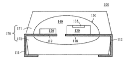
図1は、リードフレームパッケージ内のオプトカプラ100の断面図である。オプトカプラ100は、複数の導体111、112、光送信器ダイ120及び光受信器ダイ130を備える。複数の導体111、112は導電性材料からなり、該複数の導体をリードフレームから形成することができる。該複数の導体111、112は、リード線または導電性トレースとして知られている。導電性パッド118、119を形成するように該導体111、112を延長することができ、これによって、光送信器ダイ120及び光受信器ダイ130を保持するように導電性パッド118、119を構成することができる。該複数の導体111、112を、ダイ120及び130を外部回路(不図示)に接続するための手段として構成することができる。たとえば、該複数の導体111、112を、オプトカプラ100のエッジまたは底部まで延長することによって、該複数の導体が、外部回路(不図示)に対する電気接点として機能するようにすることができる。
FIG. 1 is a cross-sectional view of an
光送信器ダイ120を、発光ダイオード(以下LEDと記す)、または、光を放出することができる任意の光源とすることができる。光送信器ダイ120を、埋め込み式LED及び駆動回路を有する集積回路とすることができる。設計要件に依存して、制御回路を光送信器ダイ120に一体化することができる。光送信器ダイ120を、導体111を介して第1の電源(不図示)によって電力が供給されるように構成することができる。光送信器ダイ120は、該第1の電源(不図示)で動作する外部回路(不図示)からの論理信号にしたがって光を放出するように動作することができる。たとえば、論理信号「高」を、導体111を介して光送信器ダイ120に送信することができる。これに応答して、光送信器ダイ120は、「高」信号を示す光出力を放出する。
The optical transmitter die 120 can be a light emitting diode (hereinafter referred to as an LED) or any light source capable of emitting light. The optical transmitter die 120 can be an integrated circuit with embedded LEDs and drive circuitry. Depending on design requirements, the control circuitry can be integrated into the optical transmitter die 120. The optical transmitter die 120 can be configured to be powered by a first power source (not shown) via a
光受信器ダイ130は、フォトダイオードまたはフォトトランジスタなどの光検出器135を備えることができる。光受信器ダイ130を、埋め込み式光検出器135、あるいは、光検出器135によって生成された光電流を増幅するための増幅回路(不図示)を有する集積回路とすることができる。設計要件に依存して、信号処理を提供するために制御回路を光受信器ダイ130に一体化することができる。光受信器ダイ130を、導体122を介して第2の電源(不図示)によって電力が供給されるように構成することができる。光受信器ダイ130は、光送信器ダイ120から放出された光の形態の信号を受信するように動作することができる。
The optical receiver die 130 can include a
光ガイド140を形成するために、光送信器ダイ120と光受信器ダイ130を、透明エポキシ(エポキシはエポキシ樹脂ともいう。以下同じ)、シリコンもしくは他の類似の材料などの透明な封入剤(本発明において封入剤をカプセル材料とすることができる)によって封入することができる。次に、透明な封入剤を不透明な(すなわち光を通さない)封入剤で封入して、上側部分171及び下側部分172からなる本体170を形成する。上側部分171及び下側部分172を、成形行程において2つの異なるツール(たとえば押型器)を用いて作製することができる。不透明な封入剤を、パッケージング(パッケージ構造)の本体170を形成するために使用されるプラスチック、セラミック、もしくは任意の他の実質的に不透明か黒色の化合物とすることができる。オプションとして、透明な封入剤を、不透明な封入剤中に封入される前に、白いエポキシ(白エポキシ)、金属材料、もしくは、それらと類似の他の反射性材料などの、光を反射することができる反射性材料150で被うことができる。
In order to form the
透明な封入剤は、光送信器ダイ120から光受信器ダイ130へと放出される光を送るための光ガイド140を形成する。液状の封入剤を加えて、光送信器ダイ120と光受信器ダイ130の両方を封入することによって、透明な封入剤を形成することができる。次に、液状の透明な封入剤を硬化させて固体にすることによって、光ガイド140を形成する。光ガイド140のサイズ(すなわち大きさ)は、加えられる液状の封入剤の量を制御することによって制御されるが、該サイズは、該液状の封入剤の粘性に大きく左右されうる。小さな光ガイド140の場合には、加えられる透明なエポキシの粘性及び量を調節することによって、過度のプロセス変動を生じることなく実質的に一貫性のある(すなわち均一なもしくは同一の)サイズ及び形状を実現することができる。しかしながら、比較的大きなダイ120及び130やマルチチャネルオプトカプラの場合には、光ガイド140のサイズ及び形状に関するプロセス変動が大きくなって、光ガイドのサイズ及び形状に一貫性がなくなってしまう(すなわち、サイズ及び形状にばらつきが生じる)場合がある。
The transparent encapsulant forms a
より一貫性のある光ガイド140を得るための1つの方法は、光ガイド140が小さくなるように、光送信器ダイ120と光受信器ダイ130の距離(間隔)をより短くすることである。これは、図2に示すように、共通の導電性パッド118、119上にそれらのダイ120、130を取り付けることによって実現することができる。しかしながら、光送信器ダイ120と光受信器ダイ130は、互いに異なる2つの電源(電力供給源)に接続されうるので、それら2つのダイ120、130の間の適切な電気的絶縁及びノイズ遮断を確保することが不可欠である。
One way to obtain a more consistent
図2は、リードフレーム型パッケージ内のオプトカプラ200の断面図である。オプトカプラ200は、複数の導体211、212、光送信器ダイ220、光受信器ダイ230、透明な封入剤によって形成された光ガイド240、並びに、上側部分271と下側部分272を有する本体270を備えている。光受信器ダイ230はさらに光検出器235を備えている。図2の実施形態に示されているように、導体211、212のうちの1つは導電性パッド218を形成するために延びている。光送信器ダイ220及び光受信器ダイ230は共通の導電性パッド218に取り付けられている。図2のオプトカプラ200は、図1のオプトカプラ100に類似しているが、光送信器ダイ220と光受信器ダイ230の両方が共通の導電性パッド218に取り付けられている点で、図1のオプトカプラ100とは少なくとも異なる。図2に示す実施形態では、光送信器ダイ220を導体211に電気的に接続することができ、光受信器ダイ230を導体212に接続することができる。
FIG. 2 is a cross-sectional view of the
図2に示す実施形態では、光送信器ダイ220は、3つの材料層225を介して導電性パッド218に取り付けられており、該3つの材料層は、2つの固定層(securing layer)の間に挟まれている隔離層(絶縁層ともいう)からなる。該隔離層は、光送信器ダイ220を、光受信器ダイ230に電気的に接続されている導電性パッド218から電気的に絶縁する機能を有する。該隔離層を、ガラス、ポリイミド、または、それらと類似の電気的絶縁材料の層とすることができる。該隔離層は、光送信器ダイ220を導電性パッド218上に保持するのに十分な接着力(または接着性)を有している場合もあれば有していない場合もある。
In the embodiment shown in FIG. 2, the optical transmitter die 220 is attached to the
固定層を、二酸化ケイ素、シリコン(ケイ素)、窒化物、ベンゾシクロブタン(BCB:benzo cyclo butane)、または、任意の他の適切な絶縁用接着剤の層とすることができる。固定層を、ダイ取り付け用途に適したエポキシ材料とすることができる。そのようなエポキシには、米国マサチューセッツ州のTra-con社によって販売されているエポキシが含まれるがそれらには限定されない。固定層は、光送信器ダイ220及び隔離層を導電性パッド218上に保持するのに十分な接着力を有する。3つの材料層225を電気的に絶縁性のものとすることができ、したがって、光受信器ダイ230に電気的に接続されている導電性パッド218から、光送信器ダイ220の電圧及びノイズを分離することができる。
The pinned layer can be silicon dioxide, silicon (silicon), nitride, benzocyclobutane (BCB), or any other suitable layer of insulating adhesive. The pinned layer can be an epoxy material suitable for die attach applications. Such epoxies include, but are not limited to, epoxies sold by Tra-con, Massachusetts, USA. The pinned layer has sufficient adhesion to hold the optical transmitter die 220 and the isolation layer on the
固定層は、製造プロセスの開始時(または製造プロセスの始め)には液状であるうるが、製造プロセスの後半で、たとえば、熱またはUV光(すなわち紫外線)にさらすことによって該固定層を硬化させて、固体の層を形成することができる。隔離層は、該固定層が液状でありうる製造プロセスの開始時(または製造プロセスの始め)に、光送信器ダイ220が導電性パッド218に物理的に接触しないようにすることができる。
The pinned layer may be liquid at the beginning of the manufacturing process (or at the beginning of the manufacturing process), but may be cured later in the manufacturing process, for example, by exposure to heat or UV light (ie, ultraviolet light). Thus, a solid layer can be formed. The isolation layer may prevent the optical transmitter die 220 from physically contacting the
図2に示す実施形態では、光送信器ダイ220は3つの材料層225を介して導電性パッド218に取り付けられており、光受信器ダイ230は導電性パッド218に直接取り付けられている。この(取り付け)構成を逆にすることもできる。どの構成を選択するかは、各ダイ220、230の相対的な高さプロファイル、熱伝導要件、電源及び接地要件などの種々の設計考慮事項に基づいて決定することができる。
In the embodiment shown in FIG. 2, the optical transmitter die 220 is attached to the
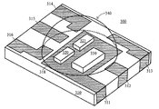
送信器ダイ220と受信器ダイ230との2つ以上の対を有するオプトカプラは、マルチチャネルオプトカプラとして知られている。図3は、ワイヤボンボンディングや不透明な封入剤のない部分的に完成されたマルチチャネルオプトカプラ300を示す。マルチチャネルオプトカプラ300は、基板310、2つの光送信器ダイ320、321、及び光受信器ダイ330を備えている。ダイ320、321及び330は、光ガイド340を形成する透明な封入剤によって封入されている。基板310をプリント回路基板(以下、PCBという)とすることができる。基板310はさらに、複数の導体311−316を備えている。PCBの場合には、導体311−316は導電性トレースとしても知られている。導体311−316のうちの1つを延長して導電性パッド318を形成することができる。光送信器ダイ320、321及び光受信器ダイ330を導電性パッド318に取り付けることができる。ダイ320、321及び330のうちの1つを導電性パッド318に直接取り付けることができ、その他のダイ320、321及び330を、図2に示す3つの絶縁材料層225によって導電性パッド318に取り付けることができる。
An optocoupler having two or more pairs of a
複数のダイ320、321及び330を同じ導電性パッド318に取り付けることによって光ガイド340のサイズを小さくすることができるが、ダイ320、321及び330の数が増えるために、光ガイド340を一貫したサイズ(すなわち、均一なまたは一定のサイズ)にすることは依然として困難な場合がある。ダイ320、321及び330の全てを封入するためには、光ガイド340のサイズが大きくなるのは避けられないであろう。一貫したサイズ及び形状を有する光ガイド340を作製するための1つの効果的な方法は、図4の実施形態に示すような光ガイド画定要素460を使用することである。
By attaching multiple dies 320, 321, and 330 to the same
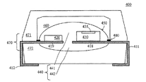
図4のオプトカプラ400は、リードフレームのリード線とすることができる複数の導体411及び412、光送信器ダイ420、光検出器435を有することができる光受信器ダイ430、ダイ420及び430を封入する透明な封入剤によって形成された光ガイド440、光ガイド画定要素460、並びに、上側部分471と下側部分472からなる、不透明な封入剤によって形成された本体470を備えている。本体470の上側部分471及び下側部分472を、成形行程において異なる2つのツール(たとえば押型器)を用いて形成することができる。同様に、光ガイド440を、上側部分441と下側部分442に分割することができる。導体411、412のいくつかを延長して、ダイ420、430を受けるための導電性パッド418、419を形成することができる。図1及び図2の実施形態にそれぞれ示されているオプトカプラ100及び200と同様に、光送信器ダイ420を第1の電源(不図示)に接続することができ、一方、光受信器ダイ430を、該第1の電源(不図示)から分離された第2の電源(不図示)に接続することができる。
The
図4に示すように、光ガイド画定要素460は、透明な封入剤によって形成された光ガイド440を画定する反射面450を有するキャビティ(すなわち空洞)を有することができる。光ガイド画定要素460は任意の適切な形状を画定することができる。しかしながら、キャビティは、一般的には実質的にドーム形である、光ガイド440に適した形状を画定することができる。光ガイド画定要素460を、ポリカーボネート、高屈折率プラスチック、アクリルプラスチック(またはアクリル合成樹脂)、または、それらに類似の任意の他の材料で形成することができる。反射面450によって光の調節をより良好に制御するために、オプションとして、マイクロ光学素子を反射面450に形成することができる。光ガイド画定要素460を、非導電性のエポキシ480を介して複数の導体411、412に取り付けることができる。そのような非導電性のエポキシ480には、Henkel社、Sumitomo Metal Mining株式会社、METAL MINING株式会社及びEpoxy Technology社によって販売されているエポキシを含めることができるが、それらには限定されない。非導電性接着剤によるダイ取り付け法や熱かしめ法(heat staking。ヒートステーキング)などの他の取り付け方法を用いて、光ガイド画定要素460を複数の導体411、412に取り付けることもできる。
As shown in FIG. 4, the light
図4に示す実施形態のオプトカプラ400を作製する1つの可能性のある方法は、先ず、ダイ420、430を導電性パッド418、419のうちの一方の側に取り付けることである。次のステップをワイヤボンディングプロセスとすることができ、該プロセスでは、ダイ420、430をそれらのそれぞれの導体411、412に結合して、電気的接続を確立することができる。図面に示されている導体より多くの導体411、412が存在しうることに留意されたい。ワイヤボンディングの後、光ガイド画定要素460を、非導電性のエポキシ480を介して導体411、412に取り付けることができ、これによって、ダイ420、430は、反射面450によって画定されたキャビティの近くに配置される。次に、液状の透明なエポキシをキャビティに注入して光ガイド440を形成する。
One possible method of making the
光ガイド440の上側部分441は、光ガイド画定要素460によって境界が定められている。信頼性を高め、かつ、ダイ420、430を完全に封入するために、注入される透明な封入剤の量を、光ガイド画定要素460のキャビティによって画定される体積よりも大きくすることができる。図4の実施形態に示すように、光ガイド440はさらに、光ガイド画定要素460のキャビティの外部に配置された下側部分442を備えている。下側部分442の形状及びサイズは、該下側部分442が光学ダイ420、430とは反対の側に配置されているため、光学的性能に及ぼす影響は比較的小さい。コストを考慮して、下側部分442のサイズ及び形状は厳密には制御されない場合がある。
The
次に、液状の透明な封入剤を硬化させて固体状態にすることができる。次に、光ガイド画定要素460、並びに、導体411、412の一部を不透明な封入剤によって封入し、第1の成形行程によって本体470の下側部分472を形成することができる。本体470の下側部分472を基板という場合がある。次に、本体470の下側部分472に第2の成形行程を施して本体470の上側部分471を形成することができる。最後に、導体411、412をリードフレーム(不図示)から分離して、要求された形状に曲げることができる。
Next, the liquid transparent encapsulant can be cured to a solid state. The light
図4の実施形態に示すように、光ガイド440の上側部分441の形状を、光ガイド画定要素460の形状に合わせて実質的にドーム形とすることができる。技術的には、光ガイド440の下側部分442をほぼ平坦にすることができ、または、他の任意の便利で費用効率が高い形状にすることができる。しかしながら、信頼性を高め、かつ、アーチング(弓なりに曲がること)や層間剥離を防止するために、下側部分442を、上側部分441と同様に、より小さい、実質的にドーム形状のものにすることができる。代替的には、マイラー(商標)、ポリイミド、メリネックス(Melinex(商標))、またはそれらと類似の他の任意の材料から形成されたテープ590(図5参照)を光ガイド440の下側部分442としてまたは該下側部分442に取り付けて信頼性を高めることができる。これは図5に示されており、図5では、テープ590によって下側部分442の一部または全てが実質的に置換されている。
As shown in the embodiment of FIG. 4, the shape of the
図5は、オプトカプラ400に類似するが、信頼性を高めるためにテープ590が使用されている点でオプトカプラ400とは少なくとも異なるオプトカプラ500の1実施形態を示す。オプトカプラ500は、複数の導体511、512、光送信器ダイ520、少なくとも1つの光検出器535を有する光受信器ダイ530、光ガイド540、光ガイド画定要素560、並びに、上側部分571と下側部分572を有する本体570を備えている。光ガイド画定要素560は、非導電性のエポキシ580を介して導体511、512に取り付けられている。オプションとして、光ガイド画定要素560の反射面550は、光送信器ダイ520から放出された光を光受信器ダイ530へと導くように構成されたマイクロ光学素子を有することができる。図4に示されているように、オプトカプラ400がかなり大きな底部442を有しているのとは異なり、オプトカプラ500の光ガイド540は、図4に示されている下側部分442がほとんどない半円ドーム(semi-dome)形を画定している。一方、テープ590は、光ガイド540の構造を強化するために使用されている。テープ590を、粘着性材料(たとえば接着剤)で作ることができ、透明な封入剤が硬化された後で光ガイド540に取り付けることができる。テープ590を使用することの利点のもう1つは、テープ590によって下側部分442(図4参照)をほぼ平坦にすることができ、これによって、光ガイド540の効率を高めることができる点である。テープ590を下側部分442上でほぼ平坦にすることができるので、オプトカプラ500の高さを低くすることもできる。別の実施形態では、図5に示されているオプトカプラ500は、光ガイド画定要素560を含まないものとすることができる。光ガイド540の形状は封入剤の粘性に依存する。しかしながら、テープ590は、光ガイド540の形状及びサイズに関するプロセス変動を低減することができる。
FIG. 5 illustrates one embodiment of an
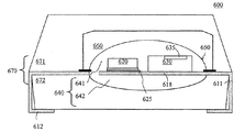
図6は、図4に示すオプトカプラ400に類似する別の実施形態であるオプトカプラ600を示す。オプトカプラ600は、複数の導体611、612(これらの導体611、612のうちの1つが共通の導電性パッド618を形成するために延びている)、光送信器ダイ620、少なくとも1つの光検出器635を有する光受信器ダイ630、透明な封入剤によって形成された光ガイド640、光ガイド画定要素660、並びに、上側部分671と下側部分672を有する本体670を備えることができる。オプションとして、マイクロ光学素子を、光ガイド画定要素660の反射面650に配置することができる。光ガイド640は、図4に示されているオプトカプラ400と同様に、上側部分641と下側部分642を有することができる。
FIG. 6 shows an
オプトカプラ600と図4に示すオプトカプラ400との1つの違いは、光送信器ダイ620と光受信器ダイ630の両方が共通の導電性パッド618に取り付けられている点である。光送信器ダイ620を、2つの固定層の間に挟まれた隔離層からなる3つの材料層625を介して、共通の導電性パッド618に取り付けることができる。光送信器ダイ620及び光受信器ダイ630を共通のパッド618に取り付けることによって、光送信器ダイ620によって放出された光が、光受信器ダイ63に到達するまでに進む距離を短くすることができる。さらに、光ガイド画定要素660は、光ガイド640が、確実に、一貫した(すなわち均一のもしくは一定の)サイズ及び形状で形成されるようにする。したがって、図6に示されている光ガイド640の効率は、理論上、図4に示す実施形態よりも高くなりうる。
One difference between the
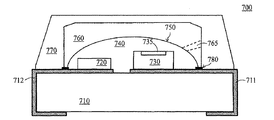
図7は、PCBを用いるオプトカプラ700の1実施形態を示す。オプトカプラ700は、基板710、光送信器ダイ720、少なくとも1つの光検出器735を有する光受信器ダイ730、反射面750を有する光ガイド740、光ガイド画定要素760、及び、不透明な封入剤770を備えている。基板710を、該基板710の両側に配置されている複数の導体711、712を有するPCBとすることができる。オプトカプラ400、500及び600とは異なり、オプトカプラ700の光ガイド画定要素760を、非導電性のエポキシ780によって基板710上の任意の場所に取り付けることができ、導体711、712だけに取り付けることには限定されない。光ガイド画定要素760は、液状の透明な封入剤を光ガイド画定要素760のキャビティに加えるための1以上の開口765をオプションとして有することができる。オプションとして、より多くの開口761を、空気逃し穴として作用するように光ガイド画定要素760に形成して、空気が該キャビティ内に閉じ込められないようにすることができる。
FIG. 7 illustrates one embodiment of an
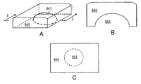
図8のA、B、及びCは、光ガイド画定要素860を異なる視点から見た図である。図8のAは、光ガイド画定要素860の斜視図である。図8のBは、図8のAの3−3の線に沿った光ガイド画定要素860の断面図である。図8のCは、光ガイド画定要素860の上面図である。光ガイド画定要素860は、ほぼドーム形状のキャビティ861を有するほぼ矩形(長方形)の形状を画定することができる。光ガイド画定要素860は、導体411、412(図4参照)または基板710(図7参照)に取り付けるのに適した任意の形状を画定することができる。キャビティ861は、図1〜図7に示されている光送信器ダイ(図7では720)から光受信器ダイ(図7では730)に向かって光を反射するのに適した任意の形状を画定することができる。オプションとして、キャビティ861を画定する表面は、反射性材料、または、半反射性材料(入射した光の一部を透過し一部を反射する材料)、または、光の分布(または配分)を制御するためのマイクロ光学素子を有することができる。典型的には、光ガイド画定要素860内には1つのキャビティ861が存在する。しかしながら、マルチチャネルオプトカプラの場合には、図9に示すように、2つ以上のキャビティ861が存在する場合がある。
8A, 8B, and 8C are views of the light
図9は、ワイヤボンディング及び不透明な封入剤のないマルチチャネルオプトカプラ900の1実施形態の上面図である。オプトカプラ900は、複数の導体911−916、複数の光送信器ダイ920、921、複数の光受信器ダイ930、931、及び、光ガイド画定要素960を備えている。光ガイド画定要素960は複数のキャビティ961、962を備えており、それぞれのキャビティが光ガイド940を画定し、それぞれのキャビティが、光送信器ダイ920、921と光受信器ダイ930、931を結合している。光送信器ダイ920と光受信器ダイ930の第1の対を、第1のキャビティ961内または該キャビティ961の近くに配置することができ、光送信器ダイ921と光受信器ダイ931の第2の対を、第2のキャビティ962内または該キャビティ962の近くに配置することができる。この構成では、送信器ダイ920と受信器ダイ930の第1の対と、送信器ダイ921と受信器ダイ931の第2の対の間のクロストークを最小限にすることができる。
FIG. 9 is a top view of one embodiment of a
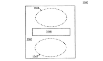
さらに、2つのキャビティ960、961を光学的に分離するために、図10に示す光分離要素1068を使用することができる。図10は、複数のキャビティ1061、1062を有する光ガイド画定要素1060の上面図1000である。光分離要素1068を、光ガイド画定要素1060の本体内に画定された単なる空隙(または空間)とすることができ、これによって、光を全反射することできるようにすることができる。代替的には、光分離要素1068を、光ガイド画定要素1060の本体内に画定された空隙を実質的に不透明な封入剤(たとえば、図4に示すオプトカプラ400の本体470を形成するために使用される材料)で満たすことによって形成することができる。
Furthermore, a
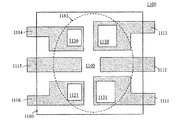
状況によっては、光送信器ダイ920、921と光受信器ダイ930、931を、図9に示すように異なるキャビティ961、962に分離しない場合がある。なぜなら、光送信器ダイ920からの信号を2つの受信器ダイ930、931の任意の1つで受信できるようにするためである。かかる状況では、1つのキャビティ960だけを使用することができる。この状況は、図11に示す実施形態に示されている。図11は、ワイヤボンディング及び不透明な封入剤がないマルチチャネルオプトカプラ1100を示している。マルチチャネルオプトカプラ1100は、複数の導体1111−1116、光送信器ダイ1120、1121、光受信器ダイ1130、1131、光ガイド画定要素1160、及び、光ガイド1140を備えている。図11に示すように、全ての光送信器ダイ1120、1121及び光受信器ダイ1130、1131を、単一のキャビティ1161中の光ガイド1140内に封入することができる。
In some situations, the optical transmitter dies 920, 921 and the optical receiver dies 930, 931 may not be separated into
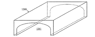
光送信器ダイ1120、1121のうちの任意の光送信器ダイから、近傍のオプトカプラ1100の光受信器ダイ1130、1131のうちの任意の光受信器ダイへと信号を送信できるようにするために、オプトカプラ1100を近傍のオプトカプラ1100に結合できる場合には、光ガイド画定要素1100が、図11に示すようなドーム形状を画定しないようにすることができる。かかる状況では、光ガイド画定要素1260は、図12に示すように、長手方向の軸の両端で終端している開口部とすることができるチャネル1261を画定することができる。近傍にある2つのオプトカプラ(不図示)のチャネル1261を同軸となるように位置合わせすることによって、2つの異なるオプトカプラ間の光通信を実現することができる。
To allow signals to be transmitted from any of the optical transmitter dies 1120, 1121 to any of the optical receiver dies 1130, 1131 of the
図13は、図4に示すオプトカプラ400の1つの可能な製造プロセスを示すフローチャート1300である。ステップ1310では、複数の導体が提供される。該複数の導体をリードフレームのリード線の形態とすることができる。ステップ1320では、光送信器ダイ及び光受信器ダイをリードフレームの1以上の導体に取り付けることができる。たとえば、ダイ取り付け用のエポキシ材料をそれらの光送信器ダイ及び光受信器ダイの背面に塗布乃至付着させた後、それらのダイをリードフレームの適切な部分に取り付けることができる。次に、方法1300はステップ1330に進むことができ、該ステップ1330において、光送信器ダイ及び光受信器ダイをリードフレームのそれぞれの導体にワイヤボンディングして電気的接続を確立できるようにする。たとえば、光送信器ダイを第1の電源に接続することができ、一方、光受信器ダイを、該第1の電源から分離乃至絶縁された第2の電源に接続することができる。
FIG. 13 is a
次に、方法1300はステップ1340に進むことができ、該ステップ1340において、光送信器ダイ及び光受信器ダイが光ガイド画定要素のキャビティ内または該キャビティの近くに配置されるように、光ガイド画定要素を、リードフレームもしくはPCB基板の導体に取り付けることができる。ステップ1350において、光送信器ダイ及び光受信器ダイを封入するために、液状の透明な封入剤が光ガイド画定要素のキャビティに注入される。該透明な封入剤は、それらのダイを導体に結合する全てのボンディングワイヤを封入して保護することもできる。
The
次に、方法1300はステップ1360に進むことができ、該ステップ1360において、透明な封入剤を固体に硬化させて光ガイドを形成することができる。オプションとして、ステップ1360の前に、光ガイドが光ガイド画定要素及び粘着テープ(または接着テープ)によって囲まれるように、該粘着テープ(または該接着テープ)を該光ガイド画定要素とは反対側のリードフレームの側に付着させることができる。
The
次に、方法1300はステップ1370に進むことができ、該ステップ1370は、第1の成形行程で開始して、導体の一部を封入するために本体の下側部分を形成する。その後、光ガイド画定要素、導体及び全てのダイを封入する(それらのダイは光ガイド画定要素及び導体に続いて封入される)本体の上側部分を形成するための別の成形行程を実施することができる。本体の上側部分と下側部分をこれとは別の順番で形成する、すなわち、上側部分を最初に形成し、次に下側部分を形成することができる。最後に、方法1300はステップ1380に進むことができ、該ステップ1380において、導体をリードフレームから切断して、特定のパッケージのリード線を形成するように曲げることができる。
The
図4に関して、光ガイド440のサイズ及び形状は、光ガイド440を作製するために使用される材料の粘性に依存しうる。しかしながら、液状の封入剤を上側部分471だけに限定すれば(すなわち、上側部分471に閉じ込めれば)、サイズ及び形状に関して一貫した(すなわち、サイズ及び形状が均一乃至一定の)光ガイド440を作製することができる。光ガイド440を本体470の上側部分471だけに限定することによって、光ガイド440を作製するのに必要な封入剤の量が少なくなる。光ガイド440の体積も大幅に小さくなる。これによって、光ガイド画定要素460を使用しなくても一貫した光ガイド440を作製することができる。さらに、光ガイド440を上側部分471だけに限定することには別の利点がある。たとえば、オプトカプラ400の高さを低くすることができる。さらに別の利点は、信頼性を高めることができるということである。光ガイド440全体の大きさを大幅に小さくすると、本体470と光ガイド440の間の相互連結メカニズム(interlocking mechanism)(の性能)が向上する。光ガイド440を上側部分471に限定するための1つの手段は、図5に示すテープ590を用いることである。しかしながら、後述する種々の実施形態において示されているように、光ガイド440を本体470の上側部分471に閉じ込めるための他の手段が存在する。
With respect to FIG. 4, the size and shape of the
図14は、オプトカプラ400に類似するオプトカプラ1400の1実施形態を示す。オプトカプラ1400は、光ガイド画定要素460を有していないが、光ガイド1440を本体1470の上側部分1471に限定するための制限要素1490を有している点で図4に示すオプトカプラ400とは少なくとも異なっている。オプトカプラ1400は、複数の導体1411、1412、光送信器ダイ1420、少なくとも1つの光検出器1435を有する光受信器ダイ1430、光ガイド1440、制限要素1490、並びに、上側部分1471と下側部分1472を有する本体1470を備えている。図14に示す実施形態では、導体1411、1412のうちの2つが延在して、光送信器ダイ1420及び光受信器ダイ1430を受けるように構成された導電性パッド1418、1419を画定することができる。しかしながら、別の実施形態では、導体1411、1412のうちの1つだけが延在して、光送信器ダイ1420と光受信器ダイ1430の両方を受けるための導電性パッド1418を画定することができる。
FIG. 14 illustrates one embodiment of an
制限要素1490は、光ガイド1440を本体1470の上側部分1471に確実に限定するように構成されている。光ガイド1440の光伝送効率は、図4に示す光ガイド440よりも高い。なぜなら、図4に示されている光ガイド440の下側部分442に起因する光損失が実質的に無いからである。さらに、光ガイド1440は、光損失を防止するための反射面1450を備えることができる。
The limiting
制限要素1490を、マイラー(商標)、ポリイミド、メリネックス(Melinex(商標))、または、図5に示すテープ590に類似の他の任意の材料から作製された絶縁テープ(または誘電体テープ)とすることができる。制限要素1490を導体1411、1412に(接着剤などで)接着することができる。代替的には、制限要素1490を、エポキシ材料または接着剤を用いて複数の導体1411、1412に取り付けられた予め成形された(または予備成形された)表面が平坦なプラスチックとすることができる。たとえば、光送信器ダイ1420及び光受信器ダイ1430を封入するための液状の封入剤が固体に硬化する前に、該封入剤中で、光ガイド1440を制限要素1490に加えることができる。この結果、光送信器ダイ1420及び光受信器ダイ1430を保持するように構成された導電性パッド1418及び1419がダイ1420、1430と制限要素1490の間にそれぞれ挟まれる。制限要素1490のサイズは通常、光ガイド1440より大きい。いくつかの場合には、制限要素1490を、光ガイド1440よりも少なくとも50%大きくすることができる。
The limiting
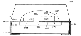
図15は、複数の導体1511、1512、光送信器ダイ1520、少なくとも1つの光検出器1535を有する光受信器ダイ1530、光ガイド1540、制限要素1590、並びに、上側部分1571と下側部分1572を有する本体1570を備えるオプトカプラ1500の1実施形態を示す。光ガイド1540は反射面1550を備えることができる。光送信器ダイ1520及び光受信器ダイ1530は導電性パッド1518、1519に取り付けられている。オプトカプラ1500は、制限要素1590がエポキシの層1595を介して複数の導体1511、1512に取り付けられている点でオプトカプラ1400とは少なくとも異なる。エポキシ1595の例には、Tra-con社のF202エポキシ、Dymax社のOP-4-20632エポキシ、または、それらと類似の任意のタイプのエポキシがある。制限要素1590を、オプトカプラ1400の制限要素1490に類似の絶縁テープ(または誘電体テープ)、または、ポリマー薄膜(polymer film)、成型プラスチックフィルム(molded plastic film)、または、他の任意の材料とすることができる。
FIG. 15 illustrates a plurality of
図16A及び図16Bは、複数の導体1611−1616、光送信器ダイ1620、少なくとも1つの光検出器1635を有する光受信器ダイ1630、反射面1650を有する光ガイド1640、制限要素1690、並びに、上側部分1671と下側部分1672を有する本体1670を備えるオプトカプラ1600の1実施形態を示す。図16Bは、ワイヤボンディング及び本体1670の上側部分1671がないオプトカプラ1600の斜視図である。図16Aは、図16Bに示されている線4−4に沿ったオプトカプラ1600の断面図である。導体1611−1616のうちの1つ(図では1611)が延在して、光送信器ダイ1620と光受信器ダイ1630の両方を受けるように構成された導電性パッド1618を画定することができる。導電性パッド1618を、光送信器ダイ1620及び光受信器ダイ1630の両方と制限要素1690との間に挟むことができ、別の実施形態では、その代わりに、導電性パッド1618を、ダイ1620と1630の一方と制限要素1690との間に挟むことができる。図16A及び図16Bに示されているように、光送信器ダイ1620と光受信器ダイ1630の両方が共通の導電性パッド1618に取り付けられているが、それらのダイは互いに異なるやり方で取り付けられている。光送信器ダイ1620は、2つの固定層の間に挟まれた隔離層からなる3つの材料層1625を介して共通の導電性パッド1618に取り付けられている。光受信器ダイ1630は共通の導電性パッド1618に直接(すなわち直に)取り付けられている。しかしながら、別の実施形態では、この(取り付け)構成は一方の取り付け構成から他方の取り付け構成に交換可能である(すなわち、光送信器ダイ1620を共通の導電性パッド1618に直接取り付け、光受信器ダイ1630を3つの材料層1625を介して共通の導電性パッド1618に取り付けるようにすることもその逆も可能である)。
16A and 16B illustrate a plurality of conductors 1611-1616, an optical transmitter die 1620, an optical receiver die 1630 having at least one
光送信器ダイ1620及び光受信器ダイ1630を共通のパッド1618に取り付けることによって、光送信器ダイ1620を光受信器ダイ1630のより近くに配置することが可能になる。この結果、オプトカプラ1600の光ガイド1640を、図14、図15にそれぞれ示されているオプトカプラ1400及び1500よりも小さくすることができる。光ガイドが光ガイド1640のようにより小さくなると、大量生産においてサイズ及び形状を一貫性のあるものにすることが可能になる。さらに、(光送信器ダイと光受信器ダイの)距離がより短くなることによって、光伝送効率がより高い光ガイド1640を製造することもできる。
Attaching the optical transmitter die 1620 and the optical receiver die 1630 to a
図16Bに示すように、光ガイド1640全体を収容するために、制限要素1690を光ガイド1640よりも大きくすることができる。別の実施形態でも、制限要素1690を光ガイド1640よりも大きくすることができる。信頼性を考慮して、制限要素1690と本体1670を確実に連結するために、制限要素1690は通常本体1670内に封入される。したがって、制限要素1690は通常、本体1670よりも小さい。
As shown in FIG. 16B, the limiting
図17は、ワイヤボンディング及び本体の上側部分のないマルチチャネルオプトカプラ1700の1実施形態の上面図である。オプトカプラ1700は、複数の導体1711−1716、複数の光送信器ダイ1720、1721、複数の光受信器ダイ1730、1731、複数の制限要素1790、1791、複数の光ガイド1740、1741、並びに、上側部分(不図示)と下側部分1772を有する本体1770を備えている。制限要素1790、1791の各々を、光ガイド1740、1741の各々をそれぞれ収容するように構成することができる。別の実施形態では、オプトカプラ1700は、光ガイド1740、1741の両方を収容するように構成された単一の制限要素1790を備えることができる。
FIG. 17 is a top view of one embodiment of a
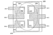
図18Aは、ワイヤボンディング及び本体1870の上側部分のないマルチチャネルオプトカプラ1800の1実施形態の上面図である。オプトカプラ1800は、複数の導体1811−1816、複数の光送信器ダイ1820、1821、複数の光受信器ダイ1830、1831、制限要素1890、光ガイド1840、並びに、上側部分(不図示)と下側部分1872を有する本体1870を備えている。全ての光送信器ダイ1820、1821及び光受信器ダイ1830、1831は単一の共通の光ガイド1840内に封入されている。光ガイド1840は1つの制限要素1890上に形成されている。単一の光ガイド1840が使用されるので、光送信器ダイ1820、1821のうちの任意のダイからの光を、光受信器ダイ1830、1831のうちの任意のダイによって受け取ることができる。
FIG. 18A is a top view of one embodiment of a
制限要素1890は通常薄い平坦な矩形物体であるが、制限要素1890は、一貫性がない(すなわち均一ではない)形状を含む任意の形状を画定することができる。たとえば、制限要素1890は、図18Bに示すような形状を有し、光ガイド1840を収容することができない一貫性のない形状を画定する。制限要素1890は、導体1811−1816に取り付けられた後、図18Cに示すように、導体1811−1816と結合して平面(平坦な表面)1895を画定する。平面1895は、本体1870の上側部分1871において光ガイド1840を収容するように構成可能である。
Although the limiting
オプトカプラ1400、1500、1600、1700、及び1800を、図13に示す方法を用いて作製することができ、その場合、ステップ1320の前またはステップ1330の後に、制限要素1490、1590、1690、1790、及び1890を取り付けるステップをオプションとして実施することができる。
以下においては、本発明の種々の構成要件の組み合わせからなる例示的な実施態様を示す。
1.光電子デバイス用のパッケージングであって、
光を放出するように構成された第1の光送信器ダイと、
前記第1の光送信器ダイによって放出された光の一部を受け取るように構成された第1の光受信器ダイと、
複数の導体であって、前記第1の光送信器ダイ及び前記第1の光受信器ダイが、該複数の導体のうちの少なくとも1つに取り付けられている、複数の導体と、
制限要素であって、前記複数の導体の前記少なくとも1つが、前記第1の光送信器ダイ及び前記第1の光受信器ダイのうちの一方と該制限要素との間に挟まれるように前記複数の導体に取り付けられた制限要素と、
前記制限要素に形成された第1の光ガイドと、
前記第1の光ガイド及び前記制限要素を封入する不透明な封入剤
を備え、
前記第1の光ガイドは、前記第1の光送信器ダイ及び前記第1の光受信器ダイを封入する実質的に透明な封入剤であり、前記第1の光ガイドは、前記第1の光送信器ダイからの光を前記第1の光受信器ダイへと伝送するように構成されている、パッケージング。
2.前記制限要素が絶縁テープである、上項1のパッケージング。
3.前記制限要素が前記複数の導体に接着される、上項1のパッケージング。
4.前記制限要素は、前記複数の導体にエポキシで取り付けられる、上項1のパッケージング。
5.前記制限要素は実質的に反射性である、上項1のパッケージング。
6.前記制限要素は前記第1の光ガイドよりも大きい、上項1のパッケージング。
7.前記制限要素は、前記複数の導体の一部に結合されて、前記第1の光ガイドを収容するように構成された表面を画定する、上項1のパッケージング。
8.前記第1の光送信器ダイと前記第1の光受信器ダイの一方が、前記複数の導体の前記少なくとも1つに直接取り付けられ、前記第1の光送信器ダイと前記第1の光受信器ダイの他方が、2つの固定層の間に挟まれた隔離層からなる3つの材料層を介して前記複数の導体のうちの少なくとも1つに取り付けられる、上項1のパッケージング。
9.第2の光送信器ダイ及び第2の光受信器ダイを備える、上項1のパッケージング。
10.前記第2の光送信器ダイ及び前記第2の光受信器ダイが前記第1の光ガイド内に封入される、上項9のパッケージング。
11.前記第2の光送信器ダイ及び前記第2の光受信器ダイを封入する第2の光ガイドをさらに備える、上項9のパッケージング。
12.前記第1の光ガイドと前記第2の光ガイドが光学的に分離されている、上項11のパッケージング。
13.第2の制限要素を備える上項11のパッケージングであって、該第2の制限要素は、前記複数の導体が、前記第2の光ガイドと、前記第2の光送信器ダイ及び前記第2の光受信器ダイとの間に挟まれるように設けられることからなる、上項11のパッケージング。
14.前記第1の光送信器ダイと前記第1の光受信器ダイが、前記複数の導体のうちの2つにそれぞれ取り付けられる、上項1のパッケージング。
15.前記パッケージングがオプトカプラの一部を形成する、上項1のパッケージング。
16.オプトカプラであって、
光を放出するように構成された第1の光送信器ダイであって、第1の外部電源から電力を得るように構成された第1の光送信器ダイと、
前記第1の光送信器ダイによって放出された光を受け取るように構成された第1の光受信器ダイであって、第2の外部電源から電力を得るように構成された第1の光受信器ダイと、
複数の導電性リード線であって、前記第1の光送信器ダイ及び前記第1の光受信器ダイが、該導電性リード線の少なくとも1つに取り付けられている、複数の導電性リード線と、
制限要素であって、該制限要素と、前記第1の光送信器ダイ及び前記第1の光受信器ダイの一方との間に挟まれている前記複数の導電性リード線の前記少なくとも1つに取り付けられた制限要素と、
前記第1の光送信器ダイ及び前記第1の光受信器ダイを封入する光ガイドであって、前記制限要素に形成された光ガイドと、
前記第1の光ガイド及び前記制限要素を封入する不透明な封入剤
を備え、
前記第1の光ガイドは、前記第1の送信器ダイから前記第1の光受信器ダイへと光を伝送するように構成されている、オプトカプラ。
17.前記制限要素が誘電体膜である、上項16のオプトカプラ。
18.前記制限要素が実質的に反射性である、上項16のオプトカプラ。
19.前記複数の導電性リード線の1つが導電性パッドを画定し、前記第1の光送信器ダイと前記第1の光受信器ダイの一方が前記導電性パッドに直接取り付けられ、前記第1の光送信器ダイと前記第1の光受信器ダイの他方が、2つの固定層の間に挟まれた隔離層からなる3つの材料層を介して前記導電性パッドに取り付けられる、上項16のオプトカプラ。
20.光電子デバイスであって、
光を放出するように構成された第1の光送信器ダイと、
前記第1の光送信器ダイによって放出された光を受け取るように構成された第1の光受信器ダイと、
複数の導電性リード線であって、前記第1の光送信器ダイ及び前記第1の光受信器ダイが、該複数の導電性リード線のうちの少なくとも1つに取り付けられている、複数の導電性リード線と、
制限要素であって、前記複数の導電性リード線の前記少なくとも1つが、前記第1の光送信器ダイ及び前記第1の光受信器ダイのうちの一方と該制限要素との間に挟まれるように、前記複数の導電性リード線の前記少なくとも1つに取り付けられた制限要素と、
前記制限要素に形成された第1の光ガイドと、
前記第1の光ガイドを封入し、及び、前記複数の導電性リード線及び前記制限要素を少なくとも部分的に封入する不透明な封入剤
を備え、
前記第1の光ガイドは、前記第1の光送信器ダイ及び前記第1の光受信器ダイを封入する実質的に透明な封入剤であり、前記第1の光ガイドは、前記第1の光送信器ダイからの光を前記第2の光受信器ダイへと伝送するように構成されている、光電子デバイス。
In the following, exemplary embodiments consisting of combinations of various constituents of the present invention are shown.
1. Packaging for optoelectronic devices,
A first optical transmitter die configured to emit light;
A first optical receiver die configured to receive a portion of the light emitted by the first optical transmitter die;
A plurality of conductors, wherein the first optical transmitter die and the first optical receiver die are attached to at least one of the plurality of conductors;
A limiting element, wherein the at least one of the plurality of conductors is sandwiched between one of the first optical transmitter die and the first optical receiver die and the limiting element. A limiting element attached to multiple conductors;
A first light guide formed on the limiting element;
An opaque encapsulant encapsulating the first light guide and the limiting element;
The first light guide is a substantially transparent encapsulant that encapsulates the first light transmitter die and the first light receiver die, and the first light guide is the first light guide. Packaging configured to transmit light from an optical transmitter die to the first optical receiver die.
2. The packaging of claim 1, wherein the limiting element is an insulating tape.
3. The packaging of claim 1, wherein the limiting element is bonded to the plurality of conductors.
4). The packaging of claim 1, wherein the limiting element is attached to the plurality of conductors with epoxy.
5. The packaging of claim 1, wherein the limiting element is substantially reflective.
6). The packaging of claim 1, wherein the limiting element is larger than the first light guide.
7). The packaging of claim 1, wherein the limiting element is coupled to a portion of the plurality of conductors to define a surface configured to receive the first light guide.
8). One of the first optical transmitter die and the first optical receiver die is directly attached to the at least one of the plurality of conductors, the first optical transmitter die and the first optical receiver The packaging of claim 1 wherein the other of the vessel dies is attached to at least one of the plurality of conductors through three layers of material comprising an isolation layer sandwiched between two fixed layers.
9. The packaging of claim 1 comprising a second optical transmitter die and a second optical receiver die.
10. The packaging of claim 9, wherein the second optical transmitter die and the second optical receiver die are encapsulated within the first light guide.
11. The packaging of claim 9, further comprising a second light guide encapsulating the second optical transmitter die and the second optical receiver die.
12 12. The packaging of item 11 above, wherein the first light guide and the second light guide are optically separated.
13. 12. The packaging of claim 11 comprising a second limiting element, wherein the second limiting element includes the plurality of conductors, the second light guide, the second optical transmitter die, and the second. The packaging according to the above item 11, which is provided so as to be sandwiched between two optical receiver dies.
14 The packaging of claim 1, wherein the first optical transmitter die and the first optical receiver die are each attached to two of the plurality of conductors.
15. The packaging of claim 1, wherein the packaging forms part of an optocoupler.
16. An optocoupler,
A first optical transmitter die configured to emit light, the first optical transmitter die configured to obtain power from a first external power source;
A first optical receiver die configured to receive light emitted by the first optical transmitter die, wherein the first optical receiver is configured to obtain power from a second external power source. A die,
A plurality of conductive leads, wherein the first optical transmitter die and the first optical receiver die are attached to at least one of the conductive leads. When,
A limiting element, said at least one of said plurality of conductive leads sandwiched between said limiting element and one of said first optical transmitter die and said first optical receiver die A limiting element attached to the
A light guide enclosing the first light transmitter die and the first light receiver die, the light guide formed on the limiting element;
An opaque encapsulant encapsulating the first light guide and the limiting element;
The first light guide is an optocoupler configured to transmit light from the first transmitter die to the first optical receiver die.
17. 17. The optocoupler according to item 16, wherein the limiting element is a dielectric film.
18. The optocoupler of claim 16, wherein the limiting element is substantially reflective.
19. One of the plurality of conductive leads defines a conductive pad, and one of the first optical transmitter die and the first optical receiver die is directly attached to the conductive pad; The other of the optical transmitter die and the first optical receiver die is attached to the conductive pad via three material layers consisting of an isolation layer sandwiched between two fixed layers. Optocoupler.
20. An optoelectronic device,
A first optical transmitter die configured to emit light;
A first optical receiver die configured to receive light emitted by the first optical transmitter die;
A plurality of conductive leads, wherein the first optical transmitter die and the first optical receiver die are attached to at least one of the plurality of conductive leads. Conductive leads,
A limiting element, wherein the at least one of the plurality of conductive leads is sandwiched between one of the first optical transmitter die and the first optical receiver die and the limiting element. A limiting element attached to the at least one of the plurality of conductive leads,
A first light guide formed on the limiting element;
An opaque encapsulant that encapsulates the first light guide and at least partially encapsulates the plurality of conductive leads and the restriction element;
The first light guide is a substantially transparent encapsulant that encapsulates the first light transmitter die and the first light receiver die, and the first light guide is the first light guide. An optoelectronic device configured to transmit light from an optical transmitter die to the second optical receiver die.
本発明の特定の実施形態を図示し説明したが、本発明は、図示し説明した部分乃至部品の特定の形態もしくは配置には限定されない。それらの図示及び説明を狭く解釈すべきではないことは明らかである。たとえば、光送信器ダイ220をLEDとすることができるが、該光送信器ダイを、LED及び回路が組み込まれたダイとすることも、将来の技術を用いた光源とすることもできる。同様に、オプトカプラが全ての実施形態において説明されているが、当業者には、共通の光ガイドに封入された光送信器ダイ及び光受信器ダイを少なくとも有する任意の他の光デバイスのパッケージングに本発明を適用できることが明らかであろう。本発明の範囲は、特許請求の範囲とその等価物によって画定されるべきものである。 While specific embodiments of the invention have been illustrated and described, the invention is not limited to the specific form or arrangement of parts or parts shown and described. Obviously, their illustration and description should not be interpreted narrowly. For example, the optical transmitter die 220 can be an LED, but the optical transmitter die can be a die incorporating an LED and circuitry, or a light source using future technology. Similarly, although optocouplers are described in all embodiments, those skilled in the art will appreciate packaging of any other optical device having at least an optical transmitter die and an optical receiver die encapsulated in a common light guide. It will be apparent that the present invention can be applied. The scope of the present invention is to be defined by the claims and their equivalents.
100 オプトカプラ
111、112 導体
120 光送信器ダイ
130 光受信器ダイ
118、119 導電性パッド
100
Claims (20)
光を放出するように構成された第1の光送信器ダイと、
前記第1の光送信器ダイによって放出された光の一部を受け取るように構成された第1の光受信器ダイと、
複数の導体であって、前記第1の光送信器ダイ及び前記第1の光受信器ダイが、該複数の導体のうちの少なくとも1つに取り付けられている、複数の導体と、
制限要素であって、前記複数の導体の前記少なくとも1つが、前記第1の光送信器ダイ及び前記第1の光受信器ダイのうちの一方と該制限要素との間に挟まれるように前記複数の導体に取り付けられた制限要素と、
前記制限要素に形成された第1の光ガイドと、
前記第1の光ガイド及び前記制限要素を封入する不透明な封入剤
を備え、
前記第1の光ガイドは、前記第1の光送信器ダイ及び前記第1の光受信器ダイを封入する実質的に透明な封入剤であり、前記第1の光ガイドは、前記第1の光送信器ダイからの光を前記第1の光受信器ダイへと伝送するように構成されている、パッケージング。 Packaging for optoelectronic devices (package structure),
A first optical transmitter die configured to emit light;
A first optical receiver die configured to receive a portion of the light emitted by the first optical transmitter die;
A plurality of conductors, wherein the first optical transmitter die and the first optical receiver die are attached to at least one of the plurality of conductors;
A limiting element, wherein the at least one of the plurality of conductors is sandwiched between one of the first optical transmitter die and the first optical receiver die and the limiting element. A limiting element attached to multiple conductors;
A first light guide formed on the limiting element;
An opaque encapsulant encapsulating the first light guide and the limiting element;
The first light guide is a substantially transparent encapsulant that encapsulates the first light transmitter die and the first light receiver die, and the first light guide is the first light guide. Packaging configured to transmit light from an optical transmitter die to the first optical receiver die.
光を放出するように構成された第1の光送信器ダイであって、第1の外部電源から電力を得るように構成された第1の光送信器ダイと、
前記第1の光送信器ダイによって放出された光を受け取るように構成された第1の光受信器ダイであって、第2の外部電源から電力を得るように構成された第1の光受信器ダイと、
複数の導電性リード線であって、前記第1の光送信器ダイ及び前記第1の光受信器ダイが、該導電性リード線の少なくとも1つに取り付けられている、複数の導電性リード線と、
制限要素であって、該制限要素と、前記第1の光送信器ダイ及び前記第1の光受信器ダイの一方との間に挟まれている前記複数の導電性リード線の前記少なくとも1つに取り付けられた制限要素と、
前記第1の光送信器ダイ及び前記第1の光受信器ダイを封入する光ガイドであって、前記制限要素に形成された光ガイドと、
前記第1の光ガイド及び前記制限要素を封入する不透明な封入剤
を備え、
前記第1の光ガイドは、前記第1の送信器ダイから前記第1の光受信器ダイへと光を伝送するように構成されている、オプトカプラ。 An optocoupler,
A first optical transmitter die configured to emit light, the first optical transmitter die configured to obtain power from a first external power source;
A first optical receiver die configured to receive light emitted by the first optical transmitter die, wherein the first optical receiver is configured to obtain power from a second external power source. A die,
A plurality of conductive leads, wherein the first optical transmitter die and the first optical receiver die are attached to at least one of the conductive leads. When,
A limiting element, said at least one of said plurality of conductive leads sandwiched between said limiting element and one of said first optical transmitter die and said first optical receiver die A limiting element attached to the
A light guide enclosing the first light transmitter die and the first light receiver die, the light guide formed on the limiting element;
An opaque encapsulant encapsulating the first light guide and the limiting element;
The first light guide is an optocoupler configured to transmit light from the first transmitter die to the first optical receiver die.
光を放出するように構成された第1の光送信器ダイと、
前記第1の光送信器ダイによって放出された光を受け取るように構成された第1の光受信器ダイと、
複数の導電性リード線であって、前記第1の光送信器ダイ及び前記第1の光受信器ダイが、該複数の導電性リード線のうちの少なくとも1つに取り付けられている、複数の導電性リード線と、
制限要素であって、前記複数の導電性リード線の前記少なくとも1つが、前記第1の光送信器ダイ及び前記第1の光受信器ダイのうちの一方と該制限要素との間に挟まれるように、前記複数の導電性リード線の前記少なくとも1つに取り付けられた制限要素と、
前記制限要素に形成された第1の光ガイドと、
前記第1の光ガイドを封入し、及び、前記複数の導電性リード線及び前記制限要素を少なくとも部分的に封入する不透明な封入剤
を備え、
前記第1の光ガイドは、前記第1の光送信器ダイ及び前記第1の光受信器ダイを封入する実質的に透明な封入剤であり、前記第1の光ガイドは、前記第1の光送信器ダイからの光を前記第2の光受信器ダイへと伝送するように構成されている、光電子デバイス。
An optoelectronic device,
A first optical transmitter die configured to emit light;
A first optical receiver die configured to receive light emitted by the first optical transmitter die;
A plurality of conductive leads, wherein the first optical transmitter die and the first optical receiver die are attached to at least one of the plurality of conductive leads. Conductive leads,
A limiting element, wherein the at least one of the plurality of conductive leads is sandwiched between one of the first optical transmitter die and the first optical receiver die and the limiting element. A limiting element attached to the at least one of the plurality of conductive leads,
A first light guide formed on the limiting element;
An opaque encapsulant that encapsulates the first light guide and at least partially encapsulates the plurality of conductive leads and the restriction element;
The first light guide is a substantially transparent encapsulant that encapsulates the first light transmitter die and the first light receiver die, and the first light guide is the first light guide. An optoelectronic device configured to transmit light from an optical transmitter die to the second optical receiver die.
Applications Claiming Priority (2)
| Application Number | Priority Date | Filing Date | Title |
|---|---|---|---|
| US13/314,023 | 2011-12-07 | ||
| US13/314,023 US8577190B2 (en) | 2010-03-23 | 2011-12-07 | Optocoupler |
Publications (2)
| Publication Number | Publication Date |
|---|---|
| JP2013120940A true JP2013120940A (en) | 2013-06-17 |
| JP2013120940A5 JP2013120940A5 (en) | 2015-12-24 |
Family
ID=48549382
Family Applications (1)
| Application Number | Title | Priority Date | Filing Date |
|---|---|---|---|
| JP2012264236A Withdrawn JP2013120940A (en) | 2011-12-07 | 2012-12-03 | Optocoupler |
Country Status (2)
| Country | Link |
|---|---|
| JP (1) | JP2013120940A (en) |
| CN (1) | CN103151419A (en) |
Cited By (2)
| Publication number | Priority date | Publication date | Assignee | Title |
|---|---|---|---|---|
| CN107799512A (en) * | 2017-11-28 | 2018-03-13 | 无锡豪帮高科股份有限公司 | A kind of three-dimensional encapsulation integrates the structure and its method of photoelectric coupled circuit |
| DE112022003053T5 (en) | 2021-06-14 | 2024-04-04 | Rohm Co., Ltd. | ISOLATION MODULE |
Families Citing this family (7)
| Publication number | Priority date | Publication date | Assignee | Title |
|---|---|---|---|---|
| JP6445947B2 (en) | 2015-09-04 | 2018-12-26 | 株式会社東芝 | Optical coupling device |
| US10074639B2 (en) * | 2016-12-30 | 2018-09-11 | Texas Instruments Incorporated | Isolator integrated circuits with package structure cavity and fabrication methods |
| US10367502B2 (en) * | 2017-04-25 | 2019-07-30 | Avago Technologies International Sales Pte. Limited | Isolation device with half duplex channel |
| CN108155106A (en) * | 2017-12-22 | 2018-06-12 | 珠海市大鹏电子科技有限公司 | A kind of length climbs the preparation process of electric light electric coupler |
| CN108091613B (en) * | 2017-12-25 | 2020-01-24 | 无锡少小科技有限公司 | Method for adjusting amplification power of photoelectric coupler |
| DE112019003834T5 (en) * | 2018-07-31 | 2021-05-06 | Ams Sensors Asia Pte. Ltd. | HOUSING INCLUDING PORTIONS OF A LEAD FRAME AS ELECTRIC POWER SUPPLIES |
| CN114141887A (en) * | 2021-11-22 | 2022-03-04 | 纽威仕微电子(无锡)有限公司 | Photoelectric conversion circuit packaging process |
-
2012
- 2012-12-03 JP JP2012264236A patent/JP2013120940A/en not_active Withdrawn
- 2012-12-07 CN CN2012105237828A patent/CN103151419A/en active Pending
Cited By (2)
| Publication number | Priority date | Publication date | Assignee | Title |
|---|---|---|---|---|
| CN107799512A (en) * | 2017-11-28 | 2018-03-13 | 无锡豪帮高科股份有限公司 | A kind of three-dimensional encapsulation integrates the structure and its method of photoelectric coupled circuit |
| DE112022003053T5 (en) | 2021-06-14 | 2024-04-04 | Rohm Co., Ltd. | ISOLATION MODULE |
Also Published As
| Publication number | Publication date |
|---|---|
| CN103151419A (en) | 2013-06-12 |
Similar Documents
| Publication | Publication Date | Title |
|---|---|---|
| US8571360B2 (en) | Optocoupler with light guide defining element | |
| JP2013120940A (en) | Optocoupler | |
| US8577190B2 (en) | Optocoupler | |
| US9236521B2 (en) | Optocoupler having lens layer | |
| US8265487B2 (en) | Half-duplex, single-fiber (S-F) optical transceiver module and method | |
| US7583867B2 (en) | Optical module | |
| US8412006B2 (en) | Optocoupler | |
| TWI228354B (en) | An optical module and a method of fabricating the same | |
| US8143637B2 (en) | Optically coupled device with an optical waveguide | |
| CN107068663B (en) | Semiconductor chip packaging with optical interface | |
| US20150262986A1 (en) | Optical coupling device | |
| US9472695B2 (en) | Opto-coupler and method of manufacturing the same | |
| ES2841409T3 (en) | Housing for semiconductor chips with optical interface | |
| US8303194B2 (en) | Transceiver and bi-directional signal transmission system thereof | |
| CN108091613B (en) | Method for adjusting amplification power of photoelectric coupler | |
| US20130313447A1 (en) | Opto-coupler | |
| JP2003008065A (en) | Method for manufacturing smd type optical element module | |
| US20140119691A1 (en) | Opto-coupler with light guide | |
| US20130087811A1 (en) | Semiconductor device and method for manufacturing the same | |
| US20170357063A1 (en) | Optical module and optical module manufacturing method | |
| JP2013065717A (en) | Semiconductor device and manufacturing method of the same | |
| US7759155B2 (en) | Optical data transceivers | |
| US8624286B2 (en) | Semiconductor device | |
| TWI546580B (en) | Optical transmission module and optical assembly | |
| KR101103336B1 (en) | Photo diode package and manufacturing method thereof |
Legal Events
| Date | Code | Title | Description |
|---|---|---|---|
| A521 | Written amendment |
Free format text: JAPANESE INTERMEDIATE CODE: A523 Effective date: 20130722 |
|
| A521 | Written amendment |
Free format text: JAPANESE INTERMEDIATE CODE: A523 Effective date: 20130731 |
|
| A521 | Written amendment |
Free format text: JAPANESE INTERMEDIATE CODE: A523 Effective date: 20151110 |
|
| A621 | Written request for application examination |
Free format text: JAPANESE INTERMEDIATE CODE: A621 Effective date: 20151110 |
|
| A977 | Report on retrieval |
Free format text: JAPANESE INTERMEDIATE CODE: A971007 Effective date: 20160622 |
|
| A761 | Written withdrawal of application |
Free format text: JAPANESE INTERMEDIATE CODE: A761 Effective date: 20160630 |