JP2012525505A - Organic evaporative material printing method and apparatus - Google Patents
Organic evaporative material printing method and apparatus Download PDFInfo
- Publication number
- JP2012525505A JP2012525505A JP2012508807A JP2012508807A JP2012525505A JP 2012525505 A JP2012525505 A JP 2012525505A JP 2012508807 A JP2012508807 A JP 2012508807A JP 2012508807 A JP2012508807 A JP 2012508807A JP 2012525505 A JP2012525505 A JP 2012525505A
- Authority
- JP
- Japan
- Prior art keywords
- thin film
- nozzle
- printing method
- organic material
- substrate
- Prior art date
- Legal status (The legal status is an assumption and is not a legal conclusion. Google has not performed a legal analysis and makes no representation as to the accuracy of the status listed.)
- Pending
Links
- 239000000463 material Substances 0.000 title claims abstract description 68
- 238000007639 printing Methods 0.000 title claims abstract description 68
- 238000000034 method Methods 0.000 title claims description 96
- 239000000758 substrate Substances 0.000 claims abstract description 53
- 238000001704 evaporation Methods 0.000 claims abstract description 36
- 238000010030 laminating Methods 0.000 claims abstract description 10
- 239000010409 thin film Substances 0.000 claims description 105
- 239000007789 gas Substances 0.000 claims description 61
- 239000011368 organic material Substances 0.000 claims description 60
- 239000012530 fluid Substances 0.000 claims description 41
- 239000012159 carrier gas Substances 0.000 claims description 34
- 238000010438 heat treatment Methods 0.000 claims description 32
- 239000010410 layer Substances 0.000 claims description 32
- 230000008020 evaporation Effects 0.000 claims description 20
- 239000000203 mixture Substances 0.000 claims description 16
- 238000012545 processing Methods 0.000 claims description 15
- 239000011364 vaporized material Substances 0.000 claims description 9
- 239000007787 solid Substances 0.000 claims description 5
- 239000010408 film Substances 0.000 claims description 4
- 239000012044 organic layer Substances 0.000 claims description 3
- 238000004891 communication Methods 0.000 claims description 2
- 238000009833 condensation Methods 0.000 claims description 2
- 230000005494 condensation Effects 0.000 claims description 2
- 238000001816 cooling Methods 0.000 claims description 2
- 238000007599 discharging Methods 0.000 claims 1
- 230000006870 function Effects 0.000 claims 1
- 238000005192 partition Methods 0.000 claims 1
- 238000003475 lamination Methods 0.000 description 9
- 238000007641 inkjet printing Methods 0.000 description 7
- 238000004519 manufacturing process Methods 0.000 description 5
- 238000007740 vapor deposition Methods 0.000 description 5
- 238000009826 distribution Methods 0.000 description 4
- 239000002904 solvent Substances 0.000 description 4
- 238000007796 conventional method Methods 0.000 description 3
- 238000005516 engineering process Methods 0.000 description 3
- 239000002245 particle Substances 0.000 description 3
- 239000011148 porous material Substances 0.000 description 3
- 230000000903 blocking effect Effects 0.000 description 2
- 239000011248 coating agent Substances 0.000 description 2
- 238000000576 coating method Methods 0.000 description 2
- 230000001276 controlling effect Effects 0.000 description 2
- 238000010586 diagram Methods 0.000 description 2
- 238000009792 diffusion process Methods 0.000 description 2
- 239000012212 insulator Substances 0.000 description 2
- 239000002648 laminated material Substances 0.000 description 2
- 239000007788 liquid Substances 0.000 description 2
- 239000012071 phase Substances 0.000 description 2
- 230000007261 regionalization Effects 0.000 description 2
- 239000002356 single layer Substances 0.000 description 2
- 238000009834 vaporization Methods 0.000 description 2
- 230000008016 vaporization Effects 0.000 description 2
- 206010037660 Pyrexia Diseases 0.000 description 1
- 230000002730 additional effect Effects 0.000 description 1
- 238000003486 chemical etching Methods 0.000 description 1
- 238000011109 contamination Methods 0.000 description 1
- 230000003247 decreasing effect Effects 0.000 description 1
- 238000000151 deposition Methods 0.000 description 1
- 230000001066 destructive effect Effects 0.000 description 1
- 238000011161 development Methods 0.000 description 1
- 230000018109 developmental process Effects 0.000 description 1
- 238000004090 dissolution Methods 0.000 description 1
- 238000001035 drying Methods 0.000 description 1
- 239000012535 impurity Substances 0.000 description 1
- 239000007791 liquid phase Substances 0.000 description 1
- 238000003701 mechanical milling Methods 0.000 description 1
- 229910052751 metal Inorganic materials 0.000 description 1
- 239000002184 metal Substances 0.000 description 1
- 150000002739 metals Chemical class 0.000 description 1
- 238000012986 modification Methods 0.000 description 1
- 230000004048 modification Effects 0.000 description 1
- 229910052756 noble gas Inorganic materials 0.000 description 1
- 238000000059 patterning Methods 0.000 description 1
- 238000000206 photolithography Methods 0.000 description 1
- 238000002360 preparation method Methods 0.000 description 1
- 230000001737 promoting effect Effects 0.000 description 1
- 239000011241 protective layer Substances 0.000 description 1
- 230000005855 radiation Effects 0.000 description 1
- 230000001105 regulatory effect Effects 0.000 description 1
- 239000004065 semiconductor Substances 0.000 description 1
- 238000000926 separation method Methods 0.000 description 1
- 238000005507 spraying Methods 0.000 description 1
- 238000004544 sputter deposition Methods 0.000 description 1
- 238000002207 thermal evaporation Methods 0.000 description 1
- 230000017105 transposition Effects 0.000 description 1
Images


Classifications
-
- C—CHEMISTRY; METALLURGY
- C23—COATING METALLIC MATERIAL; COATING MATERIAL WITH METALLIC MATERIAL; CHEMICAL SURFACE TREATMENT; DIFFUSION TREATMENT OF METALLIC MATERIAL; COATING BY VACUUM EVAPORATION, BY SPUTTERING, BY ION IMPLANTATION OR BY CHEMICAL VAPOUR DEPOSITION, IN GENERAL; INHIBITING CORROSION OF METALLIC MATERIAL OR INCRUSTATION IN GENERAL
- C23C—COATING METALLIC MATERIAL; COATING MATERIAL WITH METALLIC MATERIAL; SURFACE TREATMENT OF METALLIC MATERIAL BY DIFFUSION INTO THE SURFACE, BY CHEMICAL CONVERSION OR SUBSTITUTION; COATING BY VACUUM EVAPORATION, BY SPUTTERING, BY ION IMPLANTATION OR BY CHEMICAL VAPOUR DEPOSITION, IN GENERAL
- C23C16/00—Chemical coating by decomposition of gaseous compounds, without leaving reaction products of surface material in the coating, i.e. chemical vapour deposition [CVD] processes
- C23C16/04—Coating on selected surface areas, e.g. using masks
- C23C16/042—Coating on selected surface areas, e.g. using masks using masks
-
- C—CHEMISTRY; METALLURGY
- C23—COATING METALLIC MATERIAL; COATING MATERIAL WITH METALLIC MATERIAL; CHEMICAL SURFACE TREATMENT; DIFFUSION TREATMENT OF METALLIC MATERIAL; COATING BY VACUUM EVAPORATION, BY SPUTTERING, BY ION IMPLANTATION OR BY CHEMICAL VAPOUR DEPOSITION, IN GENERAL; INHIBITING CORROSION OF METALLIC MATERIAL OR INCRUSTATION IN GENERAL
- C23C—COATING METALLIC MATERIAL; COATING MATERIAL WITH METALLIC MATERIAL; SURFACE TREATMENT OF METALLIC MATERIAL BY DIFFUSION INTO THE SURFACE, BY CHEMICAL CONVERSION OR SUBSTITUTION; COATING BY VACUUM EVAPORATION, BY SPUTTERING, BY ION IMPLANTATION OR BY CHEMICAL VAPOUR DEPOSITION, IN GENERAL
- C23C14/00—Coating by vacuum evaporation, by sputtering or by ion implantation of the coating forming material
- C23C14/04—Coating on selected surface areas, e.g. using masks
-
- C—CHEMISTRY; METALLURGY
- C23—COATING METALLIC MATERIAL; COATING MATERIAL WITH METALLIC MATERIAL; CHEMICAL SURFACE TREATMENT; DIFFUSION TREATMENT OF METALLIC MATERIAL; COATING BY VACUUM EVAPORATION, BY SPUTTERING, BY ION IMPLANTATION OR BY CHEMICAL VAPOUR DEPOSITION, IN GENERAL; INHIBITING CORROSION OF METALLIC MATERIAL OR INCRUSTATION IN GENERAL
- C23C—COATING METALLIC MATERIAL; COATING MATERIAL WITH METALLIC MATERIAL; SURFACE TREATMENT OF METALLIC MATERIAL BY DIFFUSION INTO THE SURFACE, BY CHEMICAL CONVERSION OR SUBSTITUTION; COATING BY VACUUM EVAPORATION, BY SPUTTERING, BY ION IMPLANTATION OR BY CHEMICAL VAPOUR DEPOSITION, IN GENERAL
- C23C14/00—Coating by vacuum evaporation, by sputtering or by ion implantation of the coating forming material
- C23C14/06—Coating by vacuum evaporation, by sputtering or by ion implantation of the coating forming material characterised by the coating material
- C23C14/12—Organic material
-
- C—CHEMISTRY; METALLURGY
- C23—COATING METALLIC MATERIAL; COATING MATERIAL WITH METALLIC MATERIAL; CHEMICAL SURFACE TREATMENT; DIFFUSION TREATMENT OF METALLIC MATERIAL; COATING BY VACUUM EVAPORATION, BY SPUTTERING, BY ION IMPLANTATION OR BY CHEMICAL VAPOUR DEPOSITION, IN GENERAL; INHIBITING CORROSION OF METALLIC MATERIAL OR INCRUSTATION IN GENERAL
- C23C—COATING METALLIC MATERIAL; COATING MATERIAL WITH METALLIC MATERIAL; SURFACE TREATMENT OF METALLIC MATERIAL BY DIFFUSION INTO THE SURFACE, BY CHEMICAL CONVERSION OR SUBSTITUTION; COATING BY VACUUM EVAPORATION, BY SPUTTERING, BY ION IMPLANTATION OR BY CHEMICAL VAPOUR DEPOSITION, IN GENERAL
- C23C14/00—Coating by vacuum evaporation, by sputtering or by ion implantation of the coating forming material
- C23C14/22—Coating by vacuum evaporation, by sputtering or by ion implantation of the coating forming material characterised by the process of coating
- C23C14/228—Gas flow assisted PVD deposition
-
- C—CHEMISTRY; METALLURGY
- C23—COATING METALLIC MATERIAL; COATING MATERIAL WITH METALLIC MATERIAL; CHEMICAL SURFACE TREATMENT; DIFFUSION TREATMENT OF METALLIC MATERIAL; COATING BY VACUUM EVAPORATION, BY SPUTTERING, BY ION IMPLANTATION OR BY CHEMICAL VAPOUR DEPOSITION, IN GENERAL; INHIBITING CORROSION OF METALLIC MATERIAL OR INCRUSTATION IN GENERAL
- C23C—COATING METALLIC MATERIAL; COATING MATERIAL WITH METALLIC MATERIAL; SURFACE TREATMENT OF METALLIC MATERIAL BY DIFFUSION INTO THE SURFACE, BY CHEMICAL CONVERSION OR SUBSTITUTION; COATING BY VACUUM EVAPORATION, BY SPUTTERING, BY ION IMPLANTATION OR BY CHEMICAL VAPOUR DEPOSITION, IN GENERAL
- C23C14/00—Coating by vacuum evaporation, by sputtering or by ion implantation of the coating forming material
- C23C14/22—Coating by vacuum evaporation, by sputtering or by ion implantation of the coating forming material characterised by the process of coating
- C23C14/24—Vacuum evaporation
-
- H—ELECTRICITY
- H10—SEMICONDUCTOR DEVICES; ELECTRIC SOLID-STATE DEVICES NOT OTHERWISE PROVIDED FOR
- H10K—ORGANIC ELECTRIC SOLID-STATE DEVICES
- H10K71/00—Manufacture or treatment specially adapted for the organic devices covered by this subclass
- H10K71/10—Deposition of organic active material
- H10K71/16—Deposition of organic active material using physical vapour deposition [PVD], e.g. vacuum deposition or sputtering
- H10K71/166—Deposition of organic active material using physical vapour deposition [PVD], e.g. vacuum deposition or sputtering using selective deposition, e.g. using a mask
-
- H—ELECTRICITY
- H10—SEMICONDUCTOR DEVICES; ELECTRIC SOLID-STATE DEVICES NOT OTHERWISE PROVIDED FOR
- H10K—ORGANIC ELECTRIC SOLID-STATE DEVICES
- H10K71/00—Manufacture or treatment specially adapted for the organic devices covered by this subclass
- H10K71/10—Deposition of organic active material
- H10K71/18—Deposition of organic active material using non-liquid printing techniques, e.g. thermal transfer printing from a donor sheet
-
- H—ELECTRICITY
- H10—SEMICONDUCTOR DEVICES; ELECTRIC SOLID-STATE DEVICES NOT OTHERWISE PROVIDED FOR
- H10K—ORGANIC ELECTRIC SOLID-STATE DEVICES
- H10K71/00—Manufacture or treatment specially adapted for the organic devices covered by this subclass
-
- H—ELECTRICITY
- H10—SEMICONDUCTOR DEVICES; ELECTRIC SOLID-STATE DEVICES NOT OTHERWISE PROVIDED FOR
- H10K—ORGANIC ELECTRIC SOLID-STATE DEVICES
- H10K71/00—Manufacture or treatment specially adapted for the organic devices covered by this subclass
- H10K71/40—Thermal treatment, e.g. annealing in the presence of a solvent vapour
Abstract
1つの実施の形態における本発明は、蒸発材料を含んだ複数の気体流を基材に送り出すという形で、蒸発材料を運ぶ第1の気体流を基材に提供して基材上で積層させること、気体流を囲む気体カーテンを形成することにより、目標印刷範囲を越えて気体流が拡散するのを防ぐこと、蒸発材料を目標印刷範囲で凝縮させること、に関する。また、別の実施の形態では、熱を利用して蒸発材料の流れと積層の厚みとを制御する。
【選択図】なしThe present invention in one embodiment provides a first gas stream carrying an evaporating material to the substrate and laminating on the substrate in the form of delivering a plurality of gas streams containing the evaporating material to the substrate. It relates to preventing the gas flow from diffusing beyond the target printing range by forming a gas curtain surrounding the gas flow and condensing the evaporating material in the target printing range. In another embodiment, heat is used to control the flow of the evaporating material and the thickness of the stack.
[Selection figure] None
Description
・関連出願の相互参照
本出願は、2009年5月1日になされた米国仮特許出願第61/174,943号(ここでの参照により全体が本明細書に援用される)に基づく優先権を主張する。
本発明は、目標とする印刷領域に厚みが実質的に均一な有機薄膜を印刷し、当該薄膜に形状加工したエッジを持たせるための方法および装置に関する。より厳密に言えば、本明細書の発明は、有機薄膜(または有機層)を印刷するための新規な方法および装置に関し、当該方法および装置は、具体的には、蒸発材料(vaporized material)を生成して目標範囲上に散布し、散布した蒸発材料を凝縮させることで、実質的に均一な薄膜を目標範囲に形成する、というものである。
Cross-reference of related applications. This application is based on US Provisional Patent Application No. 61 / 174,943, filed May 1, 2009, which is hereby incorporated by reference in its entirety. Insist.
The present invention relates to a method and an apparatus for printing an organic thin film having a substantially uniform thickness on a target printing area and giving the thin film a shaped edge. More precisely, the invention herein relates to a novel method and apparatus for printing an organic thin film (or organic layer), which specifically comprises a vaporized material. A substantially uniform thin film is formed in the target range by generating and spraying on the target range and condensing the sprayed evaporation material.
有機発光装置(OLED)の製造においては、基材に1以上の有機薄膜を積層し、薄膜積層の一番上の層と一番下の層とを電極に接続する必要がある。薄膜の厚みは考慮すべき主要問題である。積層全体の厚みは約100nmであり、個々の層については、±2%よりも優れた精度で均一に積層できれば最適である。また、薄膜純度も重要である。従来の装置では、以下の2つの方法のうち1つを用いて薄膜積層を形成している:(1)相対的真空環境で有機材料を熱気化させた後、有機材料の蒸気を基材上で凝縮させる方法;(2)有機材料を溶媒に溶かして得られる溶液で基材を被覆した後、溶媒を除去する方法。 In the manufacture of an organic light emitting device (OLED), it is necessary to stack one or more organic thin films on a substrate and connect the uppermost layer and the lowermost layer of the thin film stack to electrodes. Thin film thickness is a major issue to consider. The total thickness of the stack is about 100 nm, and it is optimal if the individual layers can be stacked uniformly with an accuracy better than ± 2%. Thin film purity is also important. In the conventional apparatus, the thin film stack is formed by using one of the following two methods: (1) After vaporizing the organic material in a relative vacuum environment, the vapor of the organic material is applied to the substrate. (2) A method of removing the solvent after coating the substrate with a solution obtained by dissolving the organic material in the solvent.
OLEDの有機薄膜の積層において考慮すべきもう1つの問題は、所望の位置に正確に薄膜を配置することである。これを実現する従来方法は2つあり、薄膜積層方法に応じて使い分けられる。熱気化させる方法の場合、シャドーマスク技法を用いて、所望の形状のOLED薄膜を形成する。シャドーマスク技法では、先ず、形状を加工した物理的マスクを基材上のある領域に配置し、その後、基材全面に薄膜を積層する、という作業が必要となる。そして、積層が完了した時点でシャドーマスクは取り外される。マスクから露出していた領域には、基材上に積層された材料のパターンが形成される。しかし、この方法は効率が悪い。薄膜が必要なのはシャドーマスクから露出した領域だけであるにも関わらず、基材全体を被覆しなければならないからである。さらに、シャドーマスクは、使用のたびに被覆が厚くなっていくので、最終的には廃棄するか、清掃作業が必要になる。そして最後に、広い面積を覆う場合、シャドーマスクは使用が難しい。マスクは、加工寸法(feature size)を小さくする目的で非常に薄く作られており、そのため構造的に不安定だからである。しかし、蒸着技術を用いれば、高い均一性および純度、そして優れた厚み制御でOLED薄膜を作ることができる。 Another problem to consider in the OLED organic thin film stacking is the precise placement of the thin film at the desired location. There are two conventional methods for realizing this, and they are properly used according to the thin film stacking method. In the case of the thermal evaporation method, an OLED thin film having a desired shape is formed using a shadow mask technique. In the shadow mask technique, first, a physical mask whose shape has been processed is arranged in a certain region on the substrate, and then a thin film is laminated on the entire surface of the substrate. Then, when the lamination is completed, the shadow mask is removed. In the area exposed from the mask, a pattern of the material laminated on the base material is formed. However, this method is inefficient. This is because the entire substrate must be coated even though only a region exposed from the shadow mask is needed. Furthermore, since the shadow mask becomes thicker every time it is used, it is eventually discarded or needs to be cleaned. Finally, shadow masks are difficult to use when covering large areas. The mask is made very thin for the purpose of reducing the feature size and is therefore structurally unstable. However, using vapor deposition techniques, OLED thin films can be made with high uniformity and purity and excellent thickness control.
溶媒積層の場合は、インクジェット印刷を用いて、OLED薄膜のパターンを積層することができる。インクジェット印刷では、有機材料を溶媒に溶かして印刷可能なインクを生成する必要がある。さらに、インクジェット印刷は、従来、単一層のOLED薄膜積層に使用が限られており、これは通常、蒸着装置で用いられる4、5層の多層積層と比較して性能が劣る。積層に限度があるのは、通常、重ねて印刷すると、下にある有機層に破壊的な溶解が生じるからである。そのため、先に形成した層が、後続の層を液状で積層する際に損傷を受けないよう、1層ごとに管理する必要があり、これによって材料や積層状態に関する選択の余地は厳しく制限される。そして更に、インクジェット印刷の場合、基材に対する最初の準備作業において、薄膜を積層しようとする範囲のうちインクを含ませる領域を規制しておく作業をしないと、厚みの均一性は蒸着で積層された薄膜に比べて貧しいものとなる。しかし、こうした領域を規制しておく作業を行うと、プロセスはコスト高かつ複雑になってしまう。また、材料品質はインクジェット印刷の方が一般的に低い。これは、乾燥プロセスの間に生じる材料の構造上の変化と、インク中に存在する材料不純物とが理由である。しかしながら、インクジェット印刷の技術を用いれば、非常に広い面積にOLED薄膜パターンを設けることができ、材料効率も良い。 In the case of solvent lamination, the OLED thin film pattern can be laminated using ink jet printing. In inkjet printing, it is necessary to produce a printable ink by dissolving an organic material in a solvent. In addition, inkjet printing has traditionally been limited to single layer OLED thin film stacks, which typically have inferior performance compared to the 4-5 layer multilayer stacks used in vapor deposition equipment. Lamination is limited because overprinting usually causes destructive dissolution in the underlying organic layer. For this reason, it is necessary to manage each layer so that the previously formed layer is not damaged when the subsequent layers are laminated in a liquid state, which severely limits the choice of materials and the state of lamination. . In addition, in the case of ink-jet printing, in the initial preparation work for the substrate, the thickness uniformity is laminated by vapor deposition unless the work for restricting the area containing the ink in the range where the thin film is to be laminated is performed. It is poor compared to thin films. However, the process of regulating these areas makes the process expensive and complex. In addition, the material quality is generally lower in ink jet printing. This is due to the structural changes in the material that occur during the drying process and the material impurities present in the ink. However, if inkjet printing technology is used, the OLED thin film pattern can be provided in a very large area, and the material efficiency is good.
従来技術のなかに、インクジェット印刷が有する広面積パターン形成能力と有機薄膜の蒸着で達成される高い均一性、純度、厚み制御とを兼ね備えるものは存在しない。インクジェットで処理された単一層OLED装置の品質は、広く市販するには適さないレベルに留まっており、また、熱気化による方法も、広い範囲を対象に実施しようとするとやはり非実用的である。よって、OLED業界にとっては、高い薄膜品質と広い面積に使えて費用効果のよい大規模性とを共に実現できる技術の開発が、大きな技術目標となっている。 None of the prior arts combines the high area pattern forming capability of ink jet printing with the high uniformity, purity, and thickness control achieved by vapor deposition of organic thin films. The quality of inkjet single-layer OLED devices remains unsuitable for widespread commercialization, and thermal vaporization methods are still impractical when trying to implement a wide range. Thus, for the OLED industry, the development of technology that can achieve both high thin film quality and large area that is cost effective and cost effective is a major technical goal.
最後に、OLED表示装置の製造においても、金属、無機半導体および/または無機絶縁体の薄膜をパターン化して積層する必要がある。従来、こうしたものの積層には、蒸着および/またはスパッタリングが用いられている。パターン形成は、事前に基材に準備(例:絶縁体を用いたパターン化被覆)を施しておいたり、上述したシャドーマスクを用いたりして実現し、さらに、未加工の基材または保護層を用いる場合には、従来技術のフォトリソグラフィを用いて実現する。これらの手法はいずれも、材料を浪費したり、追加処理の作業が必要となったりする点で、所望のパターンを直接積層する場合に比べて効率が悪い。従って、高品質で、費用効率のよい、大面積の薄膜積層を行える方法および装置、並びに材料が必要とされている。 Finally, also in the manufacture of OLED display devices, it is necessary to pattern and laminate thin films of metals, inorganic semiconductors and / or inorganic insulators. Conventionally, vapor deposition and / or sputtering is used for laminating such materials. Pattern formation is realized by preparing the substrate in advance (eg, patterned coating using an insulator), using the shadow mask described above, and further processing the raw substrate or protective layer Is used, it is realized using conventional photolithography. All of these techniques are less efficient than directly laminating a desired pattern in that materials are wasted and additional processing is required. Accordingly, there is a need for methods and apparatus and materials that can provide high quality, cost effective, large area thin film stacking.
本発明の実施の形態による、均一の厚みの薄膜を基材に印刷する装置は、以下を有する。すなわち、蒸発有機材料とキャリアガス流との混合物を送るためのノズル、複数の重複する補助流を提供するように配置され、ノズルから来た混合物を送出する複数の微小孔、そして、複数の重複する補助流を受け取り、凝縮させて薄膜とする基材、である。複数の微小孔は、互いに独立したものとすることもできる。また、複数の微小孔のうち少なくとも2つは、空洞(cavity)によって他の微小孔に連通することもできる。 An apparatus for printing a thin film having a uniform thickness on a substrate according to an embodiment of the present invention includes the following. A nozzle for sending a mixture of the evaporated organic material and the carrier gas stream, a plurality of micropores arranged to provide a plurality of overlapping auxiliary streams, delivering a mixture coming from the nozzle, and a plurality of overlapping A base material that receives and condenses the auxiliary flow to be thinned. The plurality of micropores can be independent from each other. In addition, at least two of the plurality of micropores may be communicated with other micropores by a cavity.
また、別の実施の形態において、本発明は、実質的に均一な厚みを有する薄膜の印刷方法を提供する。当該方法は、蒸発材料を運ぶ第1の気体流を提供する処理を含む。蒸発材料は有機インク組成物から成るものとすればよい。「インク」の定義は、一般に、所定量の流体成分(液相または気相)を含んだ混合物であり、こうした一般的な「インク」の例としては、気相材料の混合物、キャリアガスに液体粒子を含ませた混合物、キャリアガスに固体粒子を含ませた混合物が挙げられる。第1の気体流は第1の温度とする。第1の気体流は、各々が蒸発材料を搬送する複数の部分流に分けられる。部分流のサイズは、微小孔の断面寸法の短い方とすることができる(すなわち、通常は1μmから200μm)。部分流の断面積は通常、平均流れベクトルに直行する面における流れの面積と定義される。例えば、短辺が3μm、長辺が15μmの矩形の断面を有する長い管を部分流が流れる場合、当該部分流の断面は管の矩形の断面と一致し、その断面の短い方の寸法は約3μmである。そうして、部分流は基材に送出される。この時、あわせて第2の気体流を基材に送出することにしてもよい。第2の気体流は、目標領域において、蒸発材料を含む複数の部分流を囲む位置に流体カーテンを形成する。蒸発材料は、基材上の目標領域内で凝縮して、実質的に固体の薄膜または層を形成する。好適な実施の形態においては、基材の温度は蒸発材料の温度よりも低く、それによって凝縮が促進される。基材および部分流に対する流体カーテンの相対位置を調整することで、実質的に厚みが均一な薄膜から成る印刷層の形成が可能になる。また、流体カーテンの基材に対する相対位置を調整することで、実質的に形状加工されたエッジを薄膜に持たせることができる。 In another embodiment, the present invention provides a method for printing a thin film having a substantially uniform thickness. The method includes a process that provides a first gas stream carrying a vaporized material. The evaporation material may be made of an organic ink composition. The definition of “ink” is generally a mixture containing a predetermined amount of fluid components (liquid phase or gas phase). Examples of such common “ink” include a mixture of gas phase materials, a liquid in a carrier gas. Examples thereof include a mixture containing particles and a mixture containing carrier particles containing solid particles. The first gas flow is at a first temperature. The first gas stream is divided into a plurality of partial streams each carrying a vaporized material. The size of the partial flow can be the shorter of the cross-sectional dimensions of the micropores (ie typically 1 μm to 200 μm). The partial flow cross-sectional area is usually defined as the area of the flow in the plane orthogonal to the average flow vector. For example, when a partial flow flows through a long tube having a rectangular cross section with a short side of 3 μm and a long side of 15 μm, the cross section of the partial flow coincides with the rectangular cross section of the tube, and the shorter dimension of the cross section is about 3 μm. The partial stream is then delivered to the substrate. At this time, the second gas flow may be sent to the substrate. The second gas flow forms a fluid curtain at a position surrounding the plurality of partial flows containing the evaporation material in the target region. The evaporating material condenses within the target area on the substrate to form a substantially solid film or layer. In a preferred embodiment, the temperature of the substrate is lower than the temperature of the evaporating material, thereby promoting condensation. By adjusting the relative position of the fluid curtain with respect to the substrate and the partial flow, it is possible to form a printing layer composed of a thin film having a substantially uniform thickness. Further, by adjusting the relative position of the fluid curtain with respect to the base material, the thin film can be provided with a substantially shaped edge.
また、別の実施の形態における本発明は、蒸発材料を運ぶ第1の気体流を送る導管を有した薄膜積層装置に関する。第1の気体流はインク組成物の蒸発材料を含む。複数孔ノズルを導管と流体連通させることができる。複数孔ノズルは、第1の気体流を、各々が蒸発材料を運ぶ複数の微小部分流に分ける。また、補助ノズルが、複数の部分流を囲む位置に気体カーテンを設ける。多孔ノズルおよび補助ノズルに対する基材の相対位置を調整することで、インク組成物の蒸発材料を凝縮させ、それによって実質的に固体の薄膜を目標印刷範囲に形成することができる。また、複数の部分流同士の相対的な位置関係、および、複数の部分流の流体カーテンに対する相対的な位置を調整することで、形状加工した側面エッジを備え、実質的に均一な厚みを有する薄膜を積層することができる。 Moreover, this invention in another embodiment is related with the thin film lamination apparatus which has the conduit | pipe which sends the 1st gas flow which carries vaporization material. The first gas stream includes an evaporation material of the ink composition. A multi-hole nozzle can be in fluid communication with the conduit. The multi-hole nozzle divides the first gas stream into a plurality of micro-partial streams each carrying a vaporized material. In addition, the auxiliary nozzle provides a gas curtain at a position surrounding the plurality of partial flows. By adjusting the relative position of the substrate with respect to the perforated nozzle and the auxiliary nozzle, the evaporation material of the ink composition can be condensed, thereby forming a substantially solid thin film in the target printing range. Further, by adjusting the relative positional relationship between the plurality of partial flows and the relative position of the plurality of partial flows with respect to the fluid curtain, it has a shape-processed side edge and has a substantially uniform thickness. Thin films can be stacked.
また、さらに別の実施の形態における本発明は、厚みが均一な形状を有する薄膜の印刷方法に関する。当該方法は、基材上の印刷範囲を定める処理と、キャリアガスと所定量の有機材料とを有する第1の流れを印刷範囲に送り出し、基材上に有機材料の層を積層する処理と、プリント層のエッジを目標とする第2の流れを印刷範囲に向けて発する処理と、を含み、第1の流れの温度を基材の温度よりも高くすることにより、有機材料を印刷範囲で凝縮させる。実行例では、部分流を互いに一部が重なる状態とする。 The present invention in still another embodiment relates to a method for printing a thin film having a uniform thickness. The method includes a process of defining a print range on a substrate, a process of sending a first stream having a carrier gas and a predetermined amount of an organic material to the print range, and laminating a layer of an organic material on the substrate; A second flow directed toward the print area toward the print area, and condensing the organic material in the print area by making the temperature of the first flow higher than the temperature of the substrate. Let In the execution example, the partial flows are in a state where they partially overlap each other.
更に別の実施の形態における本発明は、印刷層に側面エッジを形成する装置に関する。当該装置は、所定量の有機材料を含んでいるキャリアガスを複数の部分流として放出する第1の放出ノズルと、目標印刷領域を有し、所定量の有機材料を受け取って凝縮させることにより縁を有する印刷層が形成される基材と、目標印刷範囲の少なくとも一部にわたり、印刷層の縁に接して実質的に形状加工された側面エッジを形成する流体カーテンを形成する第2の(補助的な)放出ノズルと、を有する。複数の部分流の位置決めによって、実質的に膜厚が均一な形状の薄膜を積層することができる。 The invention in yet another embodiment relates to an apparatus for forming side edges in a printed layer. The apparatus includes a first discharge nozzle that discharges a carrier gas containing a predetermined amount of organic material as a plurality of partial flows, a target print area, and receives and condenses the predetermined amount of organic material. And a second (auxiliary) forming a fluid curtain forming a substantially shaped side edge over at least a portion of the target print area and in contact with the edges of the print layer. A discharge nozzle. By positioning a plurality of partial flows, a thin film having a substantially uniform thickness can be laminated.
本発明の別の実施の形態は、ノズルからの有機材料の放出を制御する方法に関し、当該方法は以下の処理から成る。(a)有機材料を含むキャリアガスを、複数の孔を有する放出ノズルに供給する処理、(b)放出ノズルにおいて、各々が所定量の有機材料を含む複数の放出流を形成する処理、(c)放出ノズルを加熱することで、所定量の有機材料を放出ノズルから放出させる処理、(d)放出ノズルから熱を除去することで、放出ノズルの複数の孔の中で有機材料を凝縮させる処理、(e)処理(a)から処理(d)を繰り返して、印刷ノズルからの積層の速度を制御する処理。 Another embodiment of the invention relates to a method for controlling the release of organic material from a nozzle, the method comprising the following processes. (A) a process of supplying a carrier gas containing an organic material to a discharge nozzle having a plurality of holes; (b) a process of forming a plurality of discharge flows each containing a predetermined amount of organic material in the discharge nozzle; ) Processing to discharge a predetermined amount of organic material from the discharge nozzle by heating the discharge nozzle, (d) Processing to condense the organic material in the plurality of holes of the discharge nozzle by removing heat from the discharge nozzle , (E) A process of controlling the stacking speed from the printing nozzle by repeating the processes (a) to (d).
本発明の更に別の実施の形態による装置は、複数の微小孔を有する放出ノズルと、当該放出ノズルに所定量の有機材料を有するキャリアガスを送る導管と、微小孔の少なくとも1つを加熱する加熱部と、加熱部を調整することで、所定量の有機材料を微小孔から送り出すまたは微小孔内で凝縮させるコントローラと、を有する。
また、別の実施の形態における本発明は、蒸発有機材料を含むキャリアガス流を送出することによって側面エッジを有する薄膜を印刷する方法に関し、当該方法は、キャリアガス流および蒸発有機材料を、各々が所定量の蒸発有機材料を有する複数の部分流に分ける処理と、複数の部分流を基材表面に送出する処理とを含む。所定量の蒸発有機材料は基材表面で凝縮し、有機材料の印刷層となる。側面エッジとは、積層の実質的に直交する2つのエッジをつなぐエッジと定義することができる。
An apparatus according to still another embodiment of the present invention heats at least one of the micropores, a discharge nozzle having a plurality of micropores, a conduit for delivering a carrier gas having a predetermined amount of organic material to the discharge nozzle, and A heating unit and a controller that feeds a predetermined amount of organic material from the micropores or condenses the micropores by adjusting the heating unit.
The present invention in another embodiment also relates to a method of printing a thin film having side edges by delivering a carrier gas stream containing an evaporated organic material, the method comprising: Includes a process of dividing a plurality of partial streams having a predetermined amount of evaporated organic material and a process of delivering the plurality of partial streams to the substrate surface. A predetermined amount of the evaporated organic material is condensed on the surface of the base material to form a printed layer of the organic material. A side edge can be defined as an edge connecting two substantially orthogonal edges of a stack.
さらに別の実施の形態では、複数のノズルから成る配列を形成して薄膜を積層する。複数ノズルの配列に含まれるノズルの数はいかなるものでもよい。ノズルの数は、目標印刷範囲のサイズなどを考慮して決定すればよい。各々のノズルが多孔放出を行い、一部が重なる状態または重ならない状態で部分流を生成する。
本明細書に開示する上記及び他の実施の形態について、以下、例示的かつ非限定的な図面を参照しながら説明する。これら図面において、類似の要素には類似の参照番号を付してある。
In yet another embodiment, the thin film is laminated by forming an array of nozzles. Any number of nozzles may be included in the array of nozzles. The number of nozzles may be determined in consideration of the size of the target print range. Each nozzle performs perforated discharge and generates a partial flow with or without overlapping.
These and other embodiments disclosed herein will now be described with reference to exemplary and non-limiting drawings. In these drawings, similar elements are provided with similar reference numerals.
有機薄膜のパターン形成技術は、発光表示装置の製造を含む様々な用途において有用である。特にOLED表示装置の場合、基材上に多くのパターン層を作る必要があるため、本技術は重要である。各々の層は、各フルカラーピクセルにおける赤、緑、青のうち1色を成す。パターン形成はシャドーマスク蒸着法を用いて実施される。このようなシャドーマスク処理はコストが高く、必要な作業量も大きい。更に、誤差が生じやすく、適用可能な面積も比較的小さいと考えられている。 Organic thin film patterning techniques are useful in a variety of applications, including the manufacture of light emitting display devices. In particular, in the case of an OLED display device, the present technology is important because many pattern layers need to be formed on a substrate. Each layer forms one color of red, green, and blue in each full color pixel. Pattern formation is performed using a shadow mask deposition method. Such shadow mask processing is expensive and requires a large amount of work. Furthermore, errors are likely to occur and the applicable area is considered to be relatively small.
本発明の実施の形態は、低コストで広範囲にわたってパターン形成有機薄膜を積層する装置および方法を提供することで、従来技術のこれら問題点を克服するだけでなく、目標の印刷範囲において高い均一性を実現し、必要であれば鋭いエッジ形状を持たせる。留意すべき点として、ここに開示する本発明については、キャリアガスを用いて有機蒸発材料料を移動させる技術に関連付けて記述しているが、本発明の原理は有機蒸発材料に限定されることはなく、キャリア媒体を用いて積層材料を目的地の基材まで運ぶ種類の印刷方法全てに適用することができる。 Embodiments of the present invention not only overcome these problems of the prior art by providing an apparatus and method for laminating patterned organic thin films over a wide range at low cost, but also provide high uniformity in the target printing range. And if necessary, have a sharp edge shape. It should be noted that although the present invention disclosed herein is described in relation to a technique for transferring an organic evaporating material using a carrier gas, the principle of the present invention is limited to the organic evaporating material. Rather, it can be applied to all types of printing methods that use a carrier medium to transport the laminated material to the destination substrate.
本発明の1つの実施の形態による構成は、有機蒸発材料を含むキャリアガス流をノズルで受け入れ、当該キャリアガス流を微小分配部(微小シャワーヘッド(showerhead)と置き換え可能)において複数の部分流に分けた上で、当該部分流を複数の微小孔から基材上に向けて放出することで、実質的に均一な厚みの薄膜を積層する、というものである。キャリアガス流の温度よりも基材の温度が低いため、蒸発有機材料は凝縮する。上記微小孔を組織化することで、その各々から同時に送出される蒸発材料流により、基材上に重複した形で有機材料を積層することができる。1つの微小分配部を用いて形成した積層の断面は、連続的な、厚みがゼロではない断面とすることができ、その形状は、微小孔のサイズ、形状、パターンを適当に加工することによって制御できる。つまり、本発明の実施の形態では、複数の蒸発材料流(または部分流)を少なくとも部分的に合流させることで、均一に積層された薄膜を形成する。 According to an embodiment of the present invention, a carrier gas flow containing an organic evaporation material is received by a nozzle, and the carrier gas flow is converted into a plurality of partial flows in a minute distribution section (which can be replaced with a minute showerhead). After the separation, the partial flow is discharged from the plurality of micropores onto the base material, whereby a thin film having a substantially uniform thickness is laminated. Since the substrate temperature is lower than the temperature of the carrier gas stream, the evaporated organic material condenses. By organizing the micropores, the organic material can be laminated on the base material by the evaporating material flow simultaneously delivered from each of the micropores. The cross-section of the stack formed using one micro-distribution section can be a continuous, non-zero-thickness cross-section, and the shape can be obtained by appropriately processing the size, shape and pattern of the micro-holes. Can be controlled. That is, in the embodiment of the present invention, a plurality of vaporized material streams (or partial streams) are at least partially merged to form a uniformly stacked thin film.
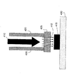
図1は、薄膜の積層に用いられる従来型のノズルを概略的に示す図である。従来の積層技術では、蒸発有機材料を運ぶのに加熱したキャリアガス流を用いている。図1における流れ110は、蒸発有機材料を含むキャリアガスを表している。流れ110に含まれて運ばれた蒸発有機材料は、基材130の上面に積層されて薄膜層115を形成する。流れ110を基材130まで送る導管は、壁120によって概略的に示してある。このように、加熱したキャリアガス流を用いることで、蒸発有機材料を管によって搬送し、ノズル125から吐出することができる。従来の用法では、基材130をノズル125に対して移動させることで所望のパターンを積層する。OLEDに用いる場合、積層薄膜の厚みは、通常10nmから200nmの範囲である。ただし、上記技術を利用する場合、積層薄膜の厚みの範囲には基本的に限界がない。
FIG. 1 is a diagram schematically showing a conventional nozzle used for laminating thin films. Conventional lamination techniques use a heated carrier gas stream to carry the evaporated organic material. A
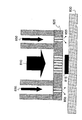
単一の開口ノズル125によって作られる薄膜の形状は、図2(A)で示すように、ガウス形状に近いものとなっている。薄膜の形状がガウス形状となった場合、通常、目標印刷領域における厚みは均一にはならない(目標印刷領域を積層範囲の中央の非常に狭い部分に限定すれば別であるが、そうした限定は普通に考えれば非現実的である)。図2(B)に示すような、鋭い側壁(側面エッジ)を備えた平らな領域に近い形とするためには、非常に細い印刷流を複数の重複する経路で送出する必要がある。しかしながら、機械配置が窮屈で許容誤差にも条件があるため、このように重複させる技術は低速かつコスト高となり、エラーも起こりやすい。また、印刷領域のエッジに鋭いエッジ形状を持たせるのに充分な細さの印刷流を生成することも困難である。
The shape of the thin film made by the
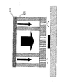
加えて、キャリアガスの温度が高く流速も速いために、材料の全てがそのまま基材上に積層されるわけではない。それどころか、基材に当たって跳ねた材料は、側面方向に流れてしまい、その結果、図3に示すように、基材上の所望の領域から遠く離れた位置に積層してしまう。このように基材が汚染されるため、当該従来技術は、大規模な製造現場はもとより、いかなる製造現場でも不人気である。 In addition, since the temperature of the carrier gas is high and the flow rate is high, not all of the materials are laminated on the substrate as they are. On the contrary, the material that bounces upon the base material flows in the lateral direction, and as a result, as shown in FIG. 3, it is laminated at a position far from a desired region on the base material. Since the base material is contaminated in this way, the related art is not popular at any manufacturing site as well as a large manufacturing site.
図4が示すのは、本発明の実施の形態による多孔ノズルである。図4における気体流410は、基材430上に積層される有機蒸発材料を運ぶ高温の気体である。気体流410は、導管420を通って多孔ノズル425に送られる。多孔ノズル425は、気体流410を複数の部分流412に分ける。各部分流412にはキャリアガスと蒸発有機材料とが含まれている。部分流412は基材430上に薄膜層415を積層する。薄膜層415は所望の形に形状加工された側面エッジを有する。また、薄膜415の厚みは実質的に均一である。最後に、多孔ノズル425は、有機蒸発材料が横方向にそれて基材を汚染するのを防ぐ。
FIG. 4 shows a multi-hole nozzle according to an embodiment of the present invention. The
この多孔ノズルは、従来の技術を用いて製造することができる。本発明の実施の形態における多孔ノズルには、非常に小さい孔(開口部)の配列が形成されており、非常に小さな点(features)で積層するというMEMS加工技術を用いて製造した。孔および点の直径は、通常、1〜10μmであるが、孔のサイズについては最大で100μmまで可能である。孔が小さく、微小サイズであることから、薄膜の積層の均一性、そして側面エッジ(鋭い側壁)は優れたものとなる。 This perforated nozzle can be manufactured using conventional techniques. The porous nozzle according to the embodiment of the present invention has an array of very small holes (openings), and is manufactured using a MEMS processing technique in which lamination is performed with very small features. The diameters of the holes and spots are usually 1-10 μm, but the hole size can be up to 100 μm. Since the pores are small and have a small size, the uniformity of the thin film stack and the side edges (sharp side walls) are excellent.
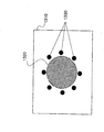
図5(A)〜5(C)は、くつかの孔パターンの例を示す。図5(A)では、複数の円形の孔が列を成して配置されている。図5(A)の多孔ノズルは、表面510に孔512が設けられている。孔512は円形の形状を有し、ノズルに対称的に配置されている。図5(B)における孔514の形状は矩形であり、図5(C)では、矩形の孔516の両側に三日月形の孔518が付属している。図5(A)〜5(C)が示しているのは、孔の形状を設計して多様な形状および向きに対応することで、積層パターンやその薄膜断面の形状を様々に処理できるということである。図5(A)〜5(C)のノズルは、MEMSなどの従来の加工技術を用いて製造することができる。
5 (A) to 5 (C) show examples of several hole patterns. In FIG. 5A, a plurality of circular holes are arranged in a row. The porous nozzle of FIG. 5A is provided with
用途によっては、微小孔パターンを単一の切れ目のない開口部(または複数の開口部)に変更する方が効果的であり、そうした変更は、計画的に2以上の微小孔を狭い通路(thin opening)でつなぐことで実現する。変更した場合の構造を図6(A)〜6(C)に示す。具体的には、図6(A)〜6(C)は、多孔ノズルのより複雑な孔パターンを示している。すなわち、図6が示すのは、複数の孔が連結されたパターンであり、それぞれ、円形の孔(図6(A))、矩形の孔(図6(B))、複雑な形状の孔(図6(C))の場合について示している。このように形状を設計することで、異なるパターンおよび所望の薄膜断面が実現できる。 Depending on the application, it may be more effective to change the micropore pattern to a single, unbroken opening (or multiple openings), which will intentionally move two or more micropores into a narrow channel (thin). This is realized by connecting with opening). The structure when changed is shown in FIGS. Specifically, FIGS. 6 (A) to 6 (C) show more complicated hole patterns of the porous nozzle. That is, FIG. 6 shows a pattern in which a plurality of holes are connected, and each of them has a circular hole (FIG. 6 (A)), a rectangular hole (FIG. 6 (B)), and a complicatedly shaped hole ( FIG. 6C shows the case. By designing the shape in this way, different patterns and desired thin film cross sections can be realized.
図7は多孔ノズルの配列の一例を示す図である。図7における基材730は多孔ノズル725の配列にまたがる形で配置されており、当該多孔ノズル725の配列は流れ710から不連続な薄膜715を積層する。流れ710は、蒸発有機材料を含んだ高温キャリアガスを含むものとする。各々の積層薄膜部分は、形状加工された側面エッジを有し、厚みは実質的に均一である。導管720は、多孔配列と一体化してもよいし、別個の構成としてもよい。本発明の別の実装の形では、導管720を完全に排除することもできる。更に別の実施の形態では、多孔ノズルを連結プレートの形に設計して、取り外し可能な状態で放出導管に連結する。複数の多孔ノズルを並べて、ノズルの配列を形成することもできる。ノズル内の配列において隣接する複数の孔の形状については、同一とする必要はない。
FIG. 7 is a diagram showing an example of the arrangement of the porous nozzles. The
図8は、補助気体流を用いる本発明の実施の形態を示す。本実施の形態において、気体流の位置は多孔ノズルの近くとなっており、それによって、蒸発材料積層の形状を更に調整することができる。補助気体流は、高温の気体流を中心に空気のカーテンを形成し、さらに有機蒸発材料の横方向の拡散を防ぐ。補助気体流はまた、側面エッジおよび積層材料の厚みの精度を高めるのに役立つ。ここで図8を参照する。第1の気体流810は、蒸発有機材料を運ぶ高温の気体流となっている。蒸発有機材料については、OLED用に構成されたインクとすることができる。気体流810の温度は約150℃〜450℃の範囲とすることができ、通常は300℃である。
FIG. 8 shows an embodiment of the present invention using an auxiliary gas flow. In the present embodiment, the position of the gas flow is close to the porous nozzle, whereby the shape of the evaporation material stack can be further adjusted. The auxiliary gas flow forms a curtain of air around the hot gas flow and further prevents lateral diffusion of the organic evaporation material. The auxiliary gas flow also helps to increase the accuracy of the side edges and the thickness of the laminate material. Reference is now made to FIG. The
気体流810はノズル825に送られる。ノズル825は複数の微小孔を有し、これら微小孔が気体流810を同数の部分流に分ける。各部分流は所定量の蒸発有機材料を運ぶ。その後、部分流は基材830に送られる。基材830の温度は第1の気体流の温度よりも低く、そのため、蒸発有機材料を基材の表面で凝縮させることができる。
積層処理と同時に、補助気体流850が、ノズル825の補助気体流用微小孔から送り出され、補助部分流855を形成する。補助部分流の温度は気体流810の温度よりも低くすることができる。また、補助部分流に蒸発有機材料を含ませる必要はない。補助気体流は、例えば、貴ガスとすることができる。微小孔のこうした配置により、補助気体流855は、目標積層範囲を中心に流体(または気体)のカーテンを形成することになる。流体のカーテンによって、凝縮後の有機蒸発材料815は、側面エッジを備えるものとなり、厚みも実質的に均一とすることができる。また、低温の気体カーテンでも、有機蒸発材料の横方向の拡散は防止される。
The
Simultaneously with the laminating process, the
図9は、本発明の実施の形態による多孔ノズルを気体カーテンと共に示す図である。図9の実施の形態は、導管920の上に中間プレート970が追加された点を除けば、実質的に図8の実施の形態と同じである。
図10は、図9に示す中間プレートの断面図である。図10に示すように、流体カーテンを形成する補助気体の入口1072は、高温キャリアガス入口1074から隔てられている。高温キャリアガスは、有機蒸発材料を含み、補助気体よりも実質的に高温とすることができる。これら入口1072、1074は、機械的ミリングや化学エッチングなどの技術を用いることで、面1070に容易に形成することができる。中間プレート1070上の入口1072、1074を重複して設けたり再配置したりすることで、多孔放出ノズルやその配列を作り出すことができる。中間プレート1070の使用により、気体送出システムは、2つの入口を有する単純な供給ライン(または供給導管)とすることができる。第1の入口は流体カーテン用の低温の補助気体を送り、第2の入口は有機蒸発材料を含んだ高温のキャリアガスを送る。中間プレートは、第1および第2の入口からの気流を多孔放出装置に取り込むための、コスト効率化を実現している。
FIG. 9 is a view showing a perforated nozzle according to an embodiment of the present invention together with a gas curtain. The embodiment of FIG. 9 is substantially the same as the embodiment of FIG. 8 except that an
10 is a cross-sectional view of the intermediate plate shown in FIG. As shown in FIG. 10, the
図11は、本発明の別の実施の形態による熱による遮断部を備えた多孔ノズルを示す。ここでは、多孔ノズル1125に要素加熱部1160が加えられている。加熱部がオン状態になると孔は加熱され、高温の気体1110が、矢印1155で示すように、ノズルから送り出される。一方、加熱部がオフ状態にある時、有機蒸発材料は孔の内表面で凝縮し、流れは妨げられる。図12はこうした状態を示しており、高温の有機蒸発材料が低温の孔の内部で凝縮して、ノズル1225の孔はふさがれている。ノズル1225のサイズが小さいため、要素加熱部はシステムを高速で加熱および冷却できるのが効果的である。ヒートシンク(図示せず)などの追加の手段を加えれば、より速やかな冷却を実現することができる。加熱手段は、対流加熱、伝導加熱、放射加熱のうち1以上を実現するものであればよい。
FIG. 11 shows a perforated nozzle with a heat blocking part according to another embodiment of the present invention. Here, an
コントローラを用いることで、急速に変化する孔の温度を制御することができる。コントローラは、1以上のメモリ回路に接続された1以上のマイクロプロセッサ回路を有するもの、とすればよい。加えて、流量調節器をシステムに組み入れて、コントローラと組み合わせることもできる。流量調節器を用いれば、加熱部1160のオン/オフに応じ、高温気体(図11における1110)の流量を任意に増減させることができる。メモリ回路には、プロセッサ回路を動作させるための命令や、加熱部および/または流量調節器の起動および停止のための命令を格納することができる。
By using a controller, the rapidly changing hole temperature can be controlled. The controller may have one or more microprocessor circuits connected to one or more memory circuits. In addition, a flow regulator can be incorporated into the system and combined with the controller. If the flow rate regulator is used, the flow rate of the high-temperature gas (1110 in FIG. 11) can be arbitrarily increased or decreased in accordance with the on / off state of the
加熱要素を組み入れ、さらに多孔ノズルに(または直接孔に)加える熱を調整することによって、ノズルを通る有機蒸気材料の流れを調整することができる。加熱部がオンであれば、材料は微小孔の中を流れ、微小孔壁で凝縮することはない。加熱部がオフであれば(ヒートシンクからの追加の効果もあって)、微小孔は充分に冷却され、材料は通過することなく壁で凝縮する。 By incorporating a heating element and adjusting the heat applied to the perforated nozzle (or directly to the holes), the flow of organic vapor material through the nozzle can be adjusted. If the heating section is on, the material will flow through the micropores and will not condense on the micropore walls. If the heating section is off (with an additional effect from the heat sink), the micropores are sufficiently cooled and the material condenses on the wall without passing through.
また、ここに開示する実施の形態の構成の組み合わせによって、更に、薄膜の厚みおよび均一性、そして側面エッジを制御することができる。例えば、ノズル加熱部と流体カーテンとを組み合わせて用いることで、積層の厚みおよび形状を更に制御することができる。あるいは、加熱部が動作している時にだけ流体カーテンを起動することで、積層の形状加工を更に強化することができる。ノズル加熱部および流体カーテンの両方を多孔ノズルと組み合わせることで、より高い精度を実現でき、薄膜積層の形状も制御できる。 Further, the thickness and uniformity of the thin film and the side edge can be further controlled by the combination of the configurations of the embodiments disclosed herein. For example, by using a combination of a nozzle heating unit and a fluid curtain, the thickness and shape of the stack can be further controlled. Alternatively, the shape processing of the stack can be further strengthened by starting the fluid curtain only when the heating unit is operating. By combining both the nozzle heating unit and the fluid curtain with the porous nozzle, higher accuracy can be realized and the shape of the thin film stack can also be controlled.
図13は、流体カーテン用の複数の開口部を備えたノズルの例を示す。具体的には、図13は、中央に円形ノズル1320を有し、当該円形ノズルの周囲に複数の孔1330が分散配置されている、という構造体1310を示している。ここで、円形ノズル1320は1つの出口を有し、孔1330は、構造体1310によって積層される有機蒸発薄膜のために流体カーテンを提供する。構造体1310には加熱部を加えてもよいが、必須ではない。留意すべき点として、ノズル1320は、本明細書で上述した多孔ノズルと置き換えることができる。図6を参照して示したように、空洞(cavity)によって2以上の微小孔1330を連結すれば、異なる形状の流体カーテンを実現することができる。
FIG. 13 shows an example of a nozzle with a plurality of openings for a fluid curtain. Specifically, FIG. 13 shows a
図14は、流体カーテンを形成するためのアパーチャを備えた、別の例のノズル1410を示す。図14において、円形ノズル1420が2つの流体ダクト1430の間に位置している。ノズル1420を通して運ばれる有機蒸発材料は、流体ダクト1430によって提供される流体カーテンで囲まれる。図14に示す構造例を反復配置すれば、複数のノズル1420を含む大型配列をダクト1430が囲む構成とすることができる。
FIG. 14 shows another
図15は、多孔ノズル1520とダクト1530とを有する放出構造体1510の例を示す。ダクト1530は流体カーテンを形成し、当該流体カーテンは、目標印刷領域を越えて蒸発有機材料が分散しないように境界を作る。前述の実施の形態と同様に、放出構造体1510を配列すれば、広い面積での積層を実現できる。図15の実施の形態には、更に加熱装置を追加してもよい。最後に、留意すべき点として、孔1520は円形とする必要はなく、印刷条件を満たすものであれば、どんな形状や形式としてもよい。
FIG. 15 shows an example of a
図16は実施の形態の一例を示し、当該実施の形態における微小孔は、一部が重なる状態で積層を行う。図16において、高温のキャリアガス流1605が、ノズル1610から微小分配部1620に送られる。ノズル1610と微小分配部1620とは一体化してもよい。あるいは、別個に構築して、個々の分配部を別々のノズルと組み合わせることもできる。微小分配部1620は、複数の微小孔1630によって、キャリアガス流1605を複数の部分流に分ける。微小孔1630は、各微小孔1630からの蒸気流が同時に、基材1650に一部が重なる状態で達して積層1640を成すように構成される。本実施の形態においては、1つの微小分配部から得られる積層の断面は、連続した、厚みもゼロではない断面1635となり、当該断面は、微小孔1630のサイズ、形状、パターンによって制御することができる。有機蒸発材料流は、厚みが実質的に均一な薄膜1640を形成する。図16の実施の形態は、単一の切れ目のない開口部ノズルを複数の微小開口部(必ずしも円形である必要はない)と置き換えることによって、従来の方法の問題点の多くを克服する。ノズルの位置に流体カーテンを設ければ、更に、上述の実施の形態による積層1640のエッジの完成度を上げることもできる。
FIG. 16 shows an example of the embodiment, and the micropores in the embodiment are stacked in a state where a part thereof overlaps. In FIG. 16, a hot
ここまで、本発明の原理を例示的な実施の形態と関連付けて説明したが、本発明の原理はこれらには限定されず、これら実施の形態の修正例、変形例または転置例も含まれる。 So far, the principles of the present invention have been described in association with exemplary embodiments, but the principles of the present invention are not limited to these, and modifications, variations, or transpositions of these embodiments are also included.
Claims (65)
第1の温度を有し、インク組成物である蒸発材料を搬送する第1の気体流を供給する処理と、
複数の微小孔を有するノズルに第1の気体流を通過させて、各々が蒸発材料を運ぶ複数の微小な部分流を形成する処理と、
基材に部分流を送出する処理と、
基材上で蒸発材料を凝縮させて固体の薄膜を形成する処理と、を含み、
前記複数の微小な部分流は、目標印刷範囲にわたって膜厚が均一な形状を有する薄膜が積層されるように相互の相対位置が決定されていること、
を特徴とする薄膜印刷方法。 A printing method for printing a thin film having a uniform thickness on a target printing range,
Providing a first gas stream having a first temperature and carrying a vaporized material that is an ink composition;
A process of passing a first gas stream through a nozzle having a plurality of micropores to form a plurality of micropartial streams each carrying a vaporized material;
Processing to send a partial flow to the substrate;
A process of condensing the evaporation material on the substrate to form a solid thin film,
The relative positions of the plurality of minute partial flows are determined so that thin films having a uniform thickness over the target printing range are laminated,
A thin film printing method.
を特徴とする請求項1に記載の薄膜印刷方法。 The evaporation material further comprises organic ink;
The thin film printing method according to claim 1.
を特徴とする請求項1に記載の薄膜印刷方法。 A process of delivering a second gas stream toward the substrate, the second gas stream enclosing a fluid curtain positioned with respect to the minute partial stream so as to surround the plurality of partial streams; Forming,
The thin film printing method according to claim 1.
を特徴とする請求項3に記載の薄膜印刷方法。 The temperature of the fluid curtain is lower than the first temperature;
The thin film printing method according to claim 3.
を特徴とする請求項1に記載の薄膜印刷方法。 A process of sending the first gas flow through the plurality of microhole nozzles, and each of the plurality of microhole nozzles functions to form a combination of a plurality of micropartial flows;
The thin film printing method according to claim 1.
を特徴とする請求項3に記載の薄膜印刷方法。 At least two of the partial streams overlap,
The thin film printing method according to claim 3.
を特徴とする請求項1に記載の薄膜印刷方法。 The temperature of the substrate is lower than the first temperature,
The thin film printing method according to claim 1.
を特徴とする請求項1に記載の薄膜印刷方法。 Multiple substreams are independent of each other;
The thin film printing method according to claim 1.
を特徴とする請求項1に記載の薄膜印刷方法。 A plurality of partial streams are continuously delivered to the substrate;
The thin film printing method according to claim 1.
を特徴とする請求項1に記載の薄膜印刷方法。 A plurality of divided flows are sent to the substrate in pulses;
The thin film printing method according to claim 1.
を特徴とする請求項1に記載の薄膜印刷方法。 The evaporative material is insoluble in the first gas stream or the second gas stream;
The thin film printing method according to claim 1.
インク組成物の蒸発材料を搬送する第1の気体流を送る導管と、
導管と流体連通した複数の微小孔を有し、第1の気体流を、各々が蒸発材料を運ぶ複数の微小な部分流に分ける多孔ノズルと、
インク組成物の蒸発材料を凝縮させて目標印刷範囲に固体の薄膜を形成するように多孔ノズルに対する相対位置が定められた基材と、を有し、
複数の部分流同士の相対位置は、膜厚が均一な形状を有した薄膜が積層されるように定められていること、
を特徴とする薄膜積層装置。 A thin film laminating apparatus,
A conduit for delivering a first gas stream carrying the vaporized material of the ink composition;
A perforated nozzle having a plurality of micropores in fluid communication with the conduit and dividing the first gas stream into a plurality of micropartial streams each carrying a vaporized material;
A substrate having a relative position with respect to the perforated nozzle so as to condense the evaporation material of the ink composition to form a solid thin film in a target printing range;
The relative positions of the plurality of partial flows are determined so that thin films having a uniform film thickness are laminated,
A thin film laminating apparatus characterized by the above.
を特徴とする請求項12に記載の薄膜形成装置。 The conduit is integrated with the perforated nozzle,
The thin film forming apparatus according to claim 12.
を特徴とする請求項12に記載の薄膜形成装置。 Further comprising an auxiliary nozzle for generating a gas curtain surrounding the plurality of divided flows;
The thin film forming apparatus according to claim 12.
を特徴とする請求項14に記載の薄膜形成装置。 The gas curtain prevents the first gas flow from spreading beyond the target printing range;
The thin film forming apparatus according to claim 14.
を特徴とする請求項14に記載の薄膜形成装置。 The auxiliary nozzle further has a single-hole nozzle that acts to form the edge of the target print area;
The thin film forming apparatus according to claim 14.
を特徴とする請求項14に記載の薄膜形成装置。 The multi-hole nozzle forms a printing layer with a uniform thickness by sending a plurality of partial flows to the target printing range.
The thin film forming apparatus according to claim 14.
を特徴とする請求項14に記載の薄膜形成装置。 The multi-hole nozzle further has a plurality of independent orifices, at least two of the plurality of holes being connected by an opening,
The thin film forming apparatus according to claim 14.
を特徴とする請求項14に記載の薄膜形成装置。 The conduit and the nozzle holes are integrated into one structure;
The thin film forming apparatus according to claim 14.
を特徴とする請求項14に記載の薄膜形成装置。 Further comprising a plurality of nozzles arranged to form a nozzle array, the nozzle array being surrounded by one or more auxiliary nozzles that provide a fluid curtain at the boundary of the target print area;
The thin film forming apparatus according to claim 14.
を特徴とする請求項14に記載の薄膜形成装置。 The partial flows are independent of each other,
The thin film forming apparatus according to claim 14.
を特徴とする請求項21に記載の薄膜形成装置。 The positional relationship of the plurality of nozzles with respect to each other is determined so that at least two of the plurality of partial flows overlap;
The thin film forming apparatus according to claim 21.
基材上の目標となる印刷範囲を定める処理と、
キャリアガスを含む第1の流れと有機蒸発材料とを印刷範囲に送って基材上に有機材料の層を積層する処理と、
第1の流れを、各々が有機蒸発材料とキャリアガスとを含む複数の微小な部分流に分ける処置と、
印刷層のエッジを目標として、第2の流れを印刷範囲に送出する処理と、を含み、
第1の流れの温度が基材の温度よりも高く、それによって有機蒸発材料を印刷範囲で凝縮させること、
を特徴とする印刷方法。 A printing method for printing a thin film having a uniform thickness,
Processing to determine the target print range on the substrate;
A process of laminating a layer of organic material on a substrate by sending a first stream containing a carrier gas and an organic evaporating material to a printing range;
Dividing the first stream into a plurality of micro-partial streams each containing an organic evaporating material and a carrier gas;
Processing to send the second stream to the print area with the edge of the print layer as a target,
The temperature of the first stream is higher than the temperature of the substrate, thereby condensing the organic evaporation material in the printing range;
A printing method characterized by the above.
を特徴とする請求項23に記載の薄膜印刷方法。 The second flow is parallel to the first flow;
The thin film printing method according to claim 23.
を特徴とする請求項23に記載の薄膜印刷方法。 The second flow is angled with respect to the first flow;
The thin film printing method according to claim 23.
を特徴とする請求項23に記載の薄膜印刷方法。 The second stream has a lower temperature than the first stream;
The thin film printing method according to claim 23.
を特徴とする請求項23に記載の薄膜印刷方法。 The second stream comprises an inert composition;
The thin film printing method according to claim 23.
を特徴とする請求項23に記載の薄膜印刷方法。 The target print range moves relative to the first flow;
The thin film printing method according to claim 23.
を特徴とする請求項23に記載の薄膜印刷方法。 The organic evaporation material is insoluble in the first stream or the second stream;
The thin film printing method according to claim 23.
を特徴とする請求項23に記載の薄膜印刷方法。 Further comprising a process of limiting the stacking of the organic evaporation material to the target print area by the second flow by simultaneously sending the second flow and the first flow to the target print area;
The thin film printing method according to claim 23.
を特徴とする請求項23に記載の薄膜印刷方法。 Further comprising delivering the second stream at an angle with respect to the target print area so that a uniform layer of organic evaporative material is deposited;
The thin film printing method according to claim 23.
所定量の有機材料を含むキャリアガスを複数の微小な部分流の形で放出する第1の放出ノズルと、
目標印刷範囲を有し、所定量の有機材料を受け取って凝縮させることにより縁を有する印刷層が形成される基材と、
目標印刷範囲の少なくとも一部にわたり、印刷層の縁に接して側面エッジを形成する、という状態で流体カーテンを形成する第2の放出ノズルと、を有し、
複数の部分流同士の位置関係と、複数の部分流の流体カーテンに対する相対位置とが、膜厚の均一な形状を有した薄膜が積層されるように定められていること、
を特徴とする形成装置。 A forming apparatus for forming a side edge on a printed layer,
A first discharge nozzle for discharging a carrier gas containing a predetermined amount of organic material in the form of a plurality of minute partial flows;
A substrate having a target print area, on which a printed layer having edges is formed by receiving and condensing a predetermined amount of organic material;
A second discharge nozzle that forms a fluid curtain with at least a portion of the target printing area forming a side edge in contact with the edge of the printed layer;
The positional relationship between the plurality of partial flows and the relative position of the plurality of partial flows with respect to the fluid curtain are determined so that a thin film having a uniform film thickness is laminated,
A forming apparatus characterized by.
を特徴とする請求項32に記載の形成装置。 The discharge nozzle is a perforated nozzle that divides the gas stream into a plurality of parallel gas streams;
The forming apparatus according to claim 32.
を特徴とする請求項32に記載の形成装置。 The discharge nozzle comprises a plurality of partial nozzles, each partial nozzle comprising a perforated nozzle that divides the gas stream into a plurality of parallel gas streams;
The forming apparatus according to claim 32.
を特徴とする請求項32に記載の形成装置。 Further comprising a conduit for sending the carrier gas to the first discharge nozzle;
The forming apparatus according to claim 32.
を特徴とする請求項32に記載の形成装置。 The first discharge nozzle further has a plurality of micro holes, and adjacent ones of the micro holes are separated by a partition;
The forming apparatus according to claim 32.
を特徴とする請求項32に記載の形成装置。 The first discharge nozzle further has a plurality of micropores, and the second discharge nozzle forms a fluid curtain surrounding the target print area, thereby flattening the surface of the print layer formed in the target print area. To do,
The forming apparatus according to claim 32.
を特徴とする請求項32に記載の形成装置。 The first discharge nozzle further includes a plurality of micropores, and the second discharge nozzle forms a fluid curtain surrounding the target print range, thereby having a side edge in the print layer formed in the target print range. Making
The forming apparatus according to claim 32.
を特徴とする請求項32に記載の形成装置。 The fluid curtain is formed by a second gas stream having a higher flow velocity than the carrier gas;
The forming apparatus according to claim 32.
を特徴とする請求項32に記載の形成装置。 The side edges further comprise a shape having a width between 1 μm and 100 μm, which width is desired to be in the range of 5-30 μm;
The forming apparatus according to claim 32.
(a)複数の孔を有する放出ノズルに有機材料を含むキャリアガスを供給する処理と、
(b)放出ノズルにおいて、複数の放出流を、各々が所定量の有機材料を含む状態で形成する処理と、
(c)放出ノズルを加熱することで放出ノズルから所定量の有機材料を放出させる処理と、
(d)放出ノズルから熱を除去することで放出ノズルの複数の孔の中で有機材料を凝縮させる処理と、
(e)処理(a)から処理(d)を繰り返して、放出ノズルからの積層の速度を制御する処理と、
を有することを特徴とする制御方法。 A control method for controlling the release of organic material from a nozzle,
(A) a process of supplying a carrier gas containing an organic material to a discharge nozzle having a plurality of holes;
(B) a process of forming a plurality of discharge streams in a state where each of the discharge nozzles contains a predetermined amount of an organic material in the discharge nozzle;
(C) a process of releasing a predetermined amount of organic material from the discharge nozzle by heating the discharge nozzle;
(D) a process of condensing the organic material in the plurality of holes of the discharge nozzle by removing heat from the discharge nozzle;
(E) A process of controlling the speed of stacking from the discharge nozzle by repeating the processes (a) to (d);
A control method characterized by comprising:
を特徴とする請求項41に記載の制御方法。 The process (c) further includes a process of intermittently heating the discharge nozzle,
42. The control method according to claim 41, wherein:
を特徴とする請求項41に記載の制御方法。 The process (c) further includes a process of condensing a predetermined amount of organic material on the substrate to form a printed organic layer;
42. The control method according to claim 41, wherein:
を特徴とする請求項43に記載の制御方法。 Further comprising processing the shape of the layer of organic material after printing by forming a fluid curtain surrounding the edges of the printed layer;
44. The control method according to claim 43.
を特徴とする請求項43に記載の制御方法。 Further comprising forming a side edge by directing a second gas vapor to the edge of the printed layer;
44. The control method according to claim 43.
複数の微小孔を有する放出ノズルと、
所定量の有機材料を含むキャリアガスを放出ノズルに送る導管と、
微小孔のうち少なくとも1つを加熱する加熱部と、
加熱部を調整することで、所定量の有機材料を微小孔から送り出すか、または、微小孔内で凝縮させるコントローラと、
を有することを特徴とする制御装置。 A control device for controlling the shape of a printed layer,
A discharge nozzle having a plurality of micropores;
A conduit for delivering a carrier gas containing a predetermined amount of organic material to a discharge nozzle;
A heating unit for heating at least one of the micropores;
By adjusting the heating unit, a predetermined amount of organic material is sent out from the micropore, or a controller that condenses in the micropore,
A control device comprising:
を特徴とする請求項46に記載の制御装置。 Further having a heat sink for removing heat from the discharge nozzle;
47. The control device according to claim 46.
を特徴とする請求項46に記載の制御装置。 Further having a heat removal means for removing heat from the discharge nozzle;
47. The control device according to claim 46.
を特徴とする請求項46に記載の制御装置。 The heating unit is one of a conduction heater, a convection heater or a radiant heater;
47. The control device according to claim 46.
を特徴とする請求項46に記載の制御装置。 Further comprising an auxiliary nozzle that generates a fluid flow that blocks a portion of the organic material that is released;
47. The control device according to claim 46.
を特徴とする請求項46に記載の制御装置。 The controller further comprises a processor circuit connected to the memory circuit, the memory circuit instructing the processor circuit to intermittently heat or cool the discharge nozzle;
47. The control device according to claim 46.
を特徴とする請求項46に記載の制御装置。 The controller further includes a processor circuit connected to the memory circuit, and generates instructions for intermittently heating the discharge nozzle, cooling the discharge nozzle, and a fluid curtain from the memory circuit to the processor circuit. At least one of instructions to guide a predetermined amount of material after release is sent,
47. The control device according to claim 46.
蒸発有機材料を含んだキャリアガス流を送出する処理と、
キャリアガス流および蒸発有機材料を、各々が所定量の蒸発有機材料を含んだ複数の微小な分割流に分配する処理と、
基材表面に向けて複数の分割流を送出する処理と、
基材表面で所定量の蒸発有機材料を凝縮させて有機材料の印刷層とする処理と、を含み、
複数の分割流は基材上で重なり、そのため、凝縮によって切れ目のない薄膜が形成されること、
を特徴とする薄膜印刷方法。 A thin film printing method,
Processing to deliver a carrier gas stream containing evaporated organic material;
Distributing the carrier gas stream and the evaporating organic material into a plurality of micro-divided streams each containing a predetermined amount of evaporating organic material;
Processing to send a plurality of divided flows toward the substrate surface;
A process of condensing a predetermined amount of the evaporated organic material on the surface of the base material to form a printed layer of the organic material,
The multiple split flows overlap on the substrate, so that condensation forms a continuous thin film,
A thin film printing method.
を特徴とする請求項53に記載の薄膜印刷方法。 Further comprising heating the carrier gas and the evaporated organic material;
54. The thin film printing method according to claim 53.
を特徴とする請求項53に記載の薄膜印刷方法。 Evaporating organic material consists of organic material,
54. The thin film printing method according to claim 53.
を特徴とする請求項53に記載の薄膜印刷方法。 The evaporating organic material consists of organic light emitting diodes,
54. The thin film printing method according to claim 53.
を特徴とする請求項53に記載の薄膜印刷方法。 Further comprising providing an auxiliary gas curtain defining a target print area on the substrate;
54. The thin film printing method according to claim 53.
を特徴とする請求項53に記載の薄膜印刷方法。 Further comprising moving the substrate relative to the plurality of split flows;
54. The thin film printing method according to claim 53.
蒸発有機材料とキャリアガス流との混合物を送るノズルと、
複数の重なる部分流を供給するように配置され、ノズルから来る混合物を更に送る複数の微小孔と、
重なる複数の部分流を受け取り、凝縮させて薄膜にする基材と、を有し、
複数の微小孔は互いに独立していること、
を特徴とする印刷装置。 A printing apparatus for printing a thin film on a substrate,
A nozzle for sending a mixture of the evaporated organic material and the carrier gas stream;
A plurality of micropores arranged to supply a plurality of overlapping partial streams, further feeding the mixture coming from the nozzle;
Receiving a plurality of overlapping partial streams and condensing them into a thin film,
That the plurality of micropores are independent of each other;
A printing apparatus characterized by the above.
を特徴とする請求項59に記載の印刷装置。 At least two of the micropores are connected to each other by a cavity;
60. The printing apparatus according to claim 59.
を特徴とする請求項59に記載の印刷装置。 A heating unit for heating at least one of the nozzle or the plurality of micro holes;
60. The printing apparatus according to claim 59.
を特徴とする請求項59に記載の印刷装置。 Further comprising auxiliary micropores forming a fluid curtain surrounding at least one micropore;
60. The printing apparatus according to claim 59.
を特徴とする請求項59に記載の印刷装置。 Further having a plurality of auxiliary micropores forming a fluid curtain surrounding the nozzle;
60. The printing apparatus according to claim 59.
を特徴とする請求項59に記載の印刷装置。 Organic ink is made of evaporated organic material,
60. The printing apparatus according to claim 59.
を特徴とする請求項59に記載の印刷装置。 The mixture of the evaporated organic material and the carrier gas has a higher temperature than the substrate,
60. The printing apparatus according to claim 59.
Applications Claiming Priority (3)
| Application Number | Priority Date | Filing Date | Title |
|---|---|---|---|
| US17494309P | 2009-05-01 | 2009-05-01 | |
| US61/174,943 | 2009-05-01 | ||
| PCT/US2010/033315 WO2010127328A2 (en) | 2009-05-01 | 2010-05-01 | Method and apparatus for organic vapor printing |
Publications (1)
| Publication Number | Publication Date |
|---|---|
| JP2012525505A true JP2012525505A (en) | 2012-10-22 |
Family
ID=43032816
Family Applications (1)
| Application Number | Title | Priority Date | Filing Date |
|---|---|---|---|
| JP2012508807A Pending JP2012525505A (en) | 2009-05-01 | 2010-05-01 | Organic evaporative material printing method and apparatus |
Country Status (6)
| Country | Link |
|---|---|
| US (2) | US8808799B2 (en) |
| EP (1) | EP2425470A2 (en) |
| JP (1) | JP2012525505A (en) |
| KR (1) | KR101441737B1 (en) |
| CN (1) | CN102414863B (en) |
| WO (1) | WO2010127328A2 (en) |
Cited By (11)
| Publication number | Priority date | Publication date | Assignee | Title |
|---|---|---|---|---|
| JP2015532222A (en) * | 2013-10-02 | 2015-11-09 | カティーバ, インコーポレイテッド | Apparatus and method for printing gap control |
| US9302513B2 (en) | 2011-08-09 | 2016-04-05 | Kateeva, Inc. | Apparatus and method for control of print gap |
| JP2017018951A (en) * | 2016-07-28 | 2017-01-26 | カティーバ, インコーポレイテッド | Device and method for control of print gap |
| US10022966B2 (en) | 2011-08-09 | 2018-07-17 | Kateeva, Inc. | Face-down printing apparatus and method |
| KR20180129690A (en) * | 2017-05-26 | 2018-12-05 | 유니버셜 디스플레이 코포레이션 | Generalized organic vapor jet depositor capable of high resolution printing and method for ovjp printing |
| US10851450B2 (en) | 2008-06-13 | 2020-12-01 | Kateeva, Inc. | Method and apparatus for load-locked printing |
| US11107712B2 (en) | 2013-12-26 | 2021-08-31 | Kateeva, Inc. | Techniques for thermal treatment of electronic devices |
| WO2022097787A1 (en) * | 2020-11-06 | 2022-05-12 | 엘지전자 주식회사 | Inkjet head device |
| US11338319B2 (en) | 2014-04-30 | 2022-05-24 | Kateeva, Inc. | Gas cushion apparatus and techniques for substrate coating |
| US11489119B2 (en) | 2014-01-21 | 2022-11-01 | Kateeva, Inc. | Apparatus and techniques for electronic device encapsulation |
| US11633968B2 (en) | 2008-06-13 | 2023-04-25 | Kateeva, Inc. | Low-particle gas enclosure systems and methods |
Families Citing this family (25)
| Publication number | Priority date | Publication date | Assignee | Title |
|---|---|---|---|---|
| US8128753B2 (en) | 2004-11-19 | 2012-03-06 | Massachusetts Institute Of Technology | Method and apparatus for depositing LED organic film |
| US8986780B2 (en) | 2004-11-19 | 2015-03-24 | Massachusetts Institute Of Technology | Method and apparatus for depositing LED organic film |
| JP5135432B2 (en) * | 2007-06-14 | 2013-02-06 | マサチューセッツ インスティテュート オブ テクノロジー | Method and apparatus for thin film lamination |
| US8556389B2 (en) | 2011-02-04 | 2013-10-15 | Kateeva, Inc. | Low-profile MEMS thermal printhead die having backside electrical connections |
| US8899171B2 (en) | 2008-06-13 | 2014-12-02 | Kateeva, Inc. | Gas enclosure assembly and system |
| US9604245B2 (en) | 2008-06-13 | 2017-03-28 | Kateeva, Inc. | Gas enclosure systems and methods utilizing an auxiliary enclosure |
| US9048344B2 (en) | 2008-06-13 | 2015-06-02 | Kateeva, Inc. | Gas enclosure assembly and system |
| US20100188457A1 (en) * | 2009-01-05 | 2010-07-29 | Madigan Connor F | Method and apparatus for controlling the temperature of an electrically-heated discharge nozzle |
| WO2010127328A2 (en) * | 2009-05-01 | 2010-11-04 | Kateeva, Inc. | Method and apparatus for organic vapor printing |
| US20110097495A1 (en) * | 2009-09-03 | 2011-04-28 | Universal Display Corporation | Organic vapor jet printing with chiller plate |
| KR101711694B1 (en) | 2011-04-08 | 2017-03-02 | 카티바, 인크. | Method and apparatus for printing using a facetted drum |
| JP2015004078A (en) * | 2011-10-18 | 2015-01-08 | 東京エレクトロン株式会社 | Film deposition apparatus and film deposition method |
| CN105239038B (en) * | 2014-06-09 | 2017-12-05 | 华中科技大学 | A kind of organic vapors film formation device and its film build method using figure nozzle |
| US11267012B2 (en) | 2014-06-25 | 2022-03-08 | Universal Display Corporation | Spatial control of vapor condensation using convection |
| EP2960059B1 (en) * | 2014-06-25 | 2018-10-24 | Universal Display Corporation | Systems and methods of modulating flow during vapor jet deposition of organic materials |
| US11220737B2 (en) | 2014-06-25 | 2022-01-11 | Universal Display Corporation | Systems and methods of modulating flow during vapor jet deposition of organic materials |
| KR101674615B1 (en) * | 2015-05-14 | 2016-11-09 | 주식회사 아바코 | Depositon apparatus |
| US10566534B2 (en) | 2015-10-12 | 2020-02-18 | Universal Display Corporation | Apparatus and method to deliver organic material via organic vapor-jet printing (OVJP) |
| CN105457843A (en) * | 2016-01-18 | 2016-04-06 | 武汉华星光电技术有限公司 | Photoresist coating device and phtoresist coating method |
| CN112941465A (en) * | 2016-07-29 | 2021-06-11 | 环球展览公司 | Deposition nozzle |
| CN106903996B (en) * | 2017-03-09 | 2020-05-29 | 京东方科技集团股份有限公司 | Printing apparatus |
| CN107419239A (en) * | 2017-07-28 | 2017-12-01 | 京东方科技集团股份有限公司 | For the shower nozzle of plated film, equipment and correlation method |
| US10998531B2 (en) * | 2017-12-12 | 2021-05-04 | Universal Display Corporation | Segmented OVJP print bar |
| CN111023317B (en) * | 2019-12-10 | 2021-09-17 | 陈巍 | Dry steam conveying spray pipe assembly for leading to air conditioner humidifying mechanism |
| KR102575677B1 (en) * | 2023-01-04 | 2023-09-06 | 주식회사 디스닉스 | Plasma Etching Apparatus for Etching Multiple Composite Materials |
Citations (9)
| Publication number | Priority date | Publication date | Assignee | Title |
|---|---|---|---|---|
| JP2002069650A (en) * | 2000-08-31 | 2002-03-08 | Applied Materials Inc | Method and apparatus for vapor phase deposition, and method and device for manufacturing semiconductor device |
| JP2004115916A (en) * | 2002-09-28 | 2004-04-15 | Korea Electronics Telecommun | Organic vapor deposition system, and organic vapor deposition method |
| JP2005082880A (en) * | 2003-09-11 | 2005-03-31 | Shoka Kagi Kofun Yugenkoshi | Film deposition apparatus for organic el light emitting device |
| JP2007154225A (en) * | 2005-12-01 | 2007-06-21 | Matsushita Electric Ind Co Ltd | Processing method, processing apparatus, and electronic device |
| JP2008144276A (en) * | 2006-12-07 | 2008-06-26 | Korea Electronics Telecommun | Organic/inorganic thin film deposition device and deposition method |
| WO2008105287A1 (en) * | 2007-02-28 | 2008-09-04 | Ulvac, Inc. | Deposition source, deposition apparatus and method for forming organic thin film |
| JP2009228091A (en) * | 2008-03-25 | 2009-10-08 | Canon Inc | Vapor deposition apparatus |
| JP2010103087A (en) * | 2008-10-22 | 2010-05-06 | Korea Advanced Inst Of Science & Technol | Organic dry jet printing head, and printing device and printing method using the same |
| WO2010078587A2 (en) * | 2009-01-05 | 2010-07-08 | Kateeva, Inc. | Rapid ink-charging of a dry ink discharge nozzle |
Family Cites Families (125)
| Publication number | Priority date | Publication date | Assignee | Title |
|---|---|---|---|---|
| IT1116334B (en) | 1977-12-28 | 1986-02-10 | Olivetti & Co Spa | IMPACT-FREE WRITING DEVICE WITH SELECTIVE EMISSION OF SOLID INK PARTICLES |
| US5202659A (en) | 1984-04-16 | 1993-04-13 | Dataproducts, Corporation | Method and apparatus for selective multi-resonant operation of an ink jet controlling dot size |
| US4751531A (en) | 1986-03-27 | 1988-06-14 | Fuji Xerox Co., Ltd. | Thermal-electrostatic ink jet recording apparatus |
| DE3769889D1 (en) | 1986-08-27 | 1991-06-13 | Hitachi Ltd | HEAT TRANSFER METHOD AND HEAT TRANSFER COLOR SHEET FOR USE IN THIS METHOD. |
| JP2575205B2 (en) | 1989-01-13 | 1997-01-22 | キヤノン株式会社 | Ink tank |
| GB8909011D0 (en) | 1989-04-20 | 1989-06-07 | Friend Richard H | Electroluminescent devices |
| JP2836749B2 (en) | 1989-05-09 | 1998-12-14 | 株式会社リコー | Liquid jet recording head |
| US6189989B1 (en) | 1993-04-12 | 2001-02-20 | Canon Kabushiki Kaisha | Embroidering using ink jet printing apparatus |
| US5405710A (en) | 1993-11-22 | 1995-04-11 | At&T Corp. | Article comprising microcavity light sources |
| US5623292A (en) | 1993-12-17 | 1997-04-22 | Videojet Systems International, Inc. | Temperature controller for ink jet printing |
| US5801721A (en) | 1994-09-09 | 1998-09-01 | Signtech U.S.A. Ltd. | Apparatus for producing an image on a first side of a substrate and a mirror image on a second side of the substrate |
| US5574485A (en) | 1994-10-13 | 1996-11-12 | Xerox Corporation | Ultrasonic liquid wiper for ink jet printhead maintenance |
| JPH08118641A (en) | 1994-10-20 | 1996-05-14 | Canon Inc | Ink jet head, ink jet head cartridge, ink jet device and ink container for ink jet head cartridge into which ink is re-injected |
| US6548956B2 (en) | 1994-12-13 | 2003-04-15 | The Trustees Of Princeton University | Transparent contacts for organic devices |
| US5707745A (en) | 1994-12-13 | 1998-01-13 | The Trustees Of Princeton University | Multicolor organic light emitting devices |
| US5703436A (en) | 1994-12-13 | 1997-12-30 | The Trustees Of Princeton University | Transparent contacts for organic devices |
| JP3575103B2 (en) | 1995-02-17 | 2004-10-13 | ソニー株式会社 | Recording method |
| US6086196A (en) | 1995-04-14 | 2000-07-11 | Sony Corporation | Printing device |
| US6586763B2 (en) | 1996-06-25 | 2003-07-01 | Northwestern University | Organic light-emitting diodes and methods for assembly and emission control |
| US5844363A (en) | 1997-01-23 | 1998-12-01 | The Trustees Of Princeton Univ. | Vacuum deposited, non-polymeric flexible organic light emitting devices |
| US6013982A (en) | 1996-12-23 | 2000-01-11 | The Trustees Of Princeton University | Multicolor display devices |
| US5834893A (en) | 1996-12-23 | 1998-11-10 | The Trustees Of Princeton University | High efficiency organic light emitting devices with light directing structures |
| US6091195A (en) | 1997-02-03 | 2000-07-18 | The Trustees Of Princeton University | Displays having mesa pixel configuration |
| US5956051A (en) | 1997-05-29 | 1999-09-21 | Pitney Bowes Inc. | Disabling a mailing machine when a print head is not installed |
| US5865860A (en) | 1997-06-20 | 1999-02-02 | Imra America, Inc. | Process for filling electrochemical cells with electrolyte |
| US6095630A (en) | 1997-07-02 | 2000-08-01 | Sony Corporation | Ink-jet printer and drive method of recording head for ink-jet printer |
| US6303238B1 (en) | 1997-12-01 | 2001-10-16 | The Trustees Of Princeton University | OLEDs doped with phosphorescent compounds |
| KR100232852B1 (en) | 1997-10-15 | 1999-12-01 | 윤종용 | Inkjet printer head and method for fabricating thereof |
| US6086679A (en) * | 1997-10-24 | 2000-07-11 | Quester Technology, Inc. | Deposition systems and processes for transport polymerization and chemical vapor deposition |
| US6453810B1 (en) | 1997-11-07 | 2002-09-24 | Speedline Technologies, Inc. | Method and apparatus for dispensing material in a printer |
| US5947022A (en) | 1997-11-07 | 1999-09-07 | Speedline Technologies, Inc. | Apparatus for dispensing material in a printer |
| US6065825A (en) | 1997-11-13 | 2000-05-23 | Eastman Kodak Company | Printer having mechanically-assisted ink droplet separation and method of using same |
| US6337102B1 (en) | 1997-11-17 | 2002-01-08 | The Trustees Of Princeton University | Low pressure vapor phase deposition of organic thin films |
| US6087196A (en) | 1998-01-30 | 2000-07-11 | The Trustees Of Princeton University | Fabrication of organic semiconductor devices using ink jet printing |
| US6326224B1 (en) | 1998-04-27 | 2001-12-04 | Motorola, Inc. | Method of purifying a primary color generated by an OED |
| EP2172976A3 (en) * | 1998-09-10 | 2010-05-05 | Mitsubishi Denki Kabushiki Kaisha | Semiconductor Device |
| US6097147A (en) | 1998-09-14 | 2000-08-01 | The Trustees Of Princeton University | Structure for high efficiency electroluminescent device |
| US6086195A (en) | 1998-09-24 | 2000-07-11 | Hewlett-Packard Company | Filter for an inkjet printhead |
| GB9822963D0 (en) | 1998-10-20 | 1998-12-16 | Agner Erik | Improvements in or relating to chromatography |
| US6250747B1 (en) | 1999-01-28 | 2001-06-26 | Hewlett-Packard Company | Print cartridge with improved back-pressure regulation |
| US6203151B1 (en) | 1999-06-08 | 2001-03-20 | Hewlett-Packard Company | Apparatus and method using ultrasonic energy to fix ink to print media |
| US6444400B1 (en) | 1999-08-23 | 2002-09-03 | Agfa-Gevaert | Method of making an electroconductive pattern on a support |
| US6294398B1 (en) | 1999-11-23 | 2001-09-25 | The Trustees Of Princeton University | Method for patterning devices |
| KR100319772B1 (en) | 1999-12-02 | 2002-01-09 | 오길록 | Organic Micro-Cavity Laser |
| US6312083B1 (en) | 1999-12-20 | 2001-11-06 | Xerox Corporation | Printhead assembly with ink monitoring system |
| US6276782B1 (en) | 2000-01-11 | 2001-08-21 | Eastman Kodak Company | Assisted drop-on-demand inkjet printer |
| US7194197B1 (en) * | 2000-03-16 | 2007-03-20 | Global Solar Energy, Inc. | Nozzle-based, vapor-phase, plume delivery structure for use in production of thin-film deposition layer |
| KR100408269B1 (en) | 2000-07-20 | 2003-12-01 | 삼성전자주식회사 | Ink jet print head |
| US6755519B2 (en) | 2000-08-30 | 2004-06-29 | Creo Inc. | Method for imaging with UV curable inks |
| US6601936B2 (en) | 2000-11-14 | 2003-08-05 | Cypress Semiconductor Corp. | Real time adaptive inkjet temperature regulation controller |
| CN1398360A (en) * | 2000-11-27 | 2003-02-19 | 皇家菲利浦电子有限公司 | Optical switching device |
| US6513903B2 (en) | 2000-12-29 | 2003-02-04 | Eastman Kodak Company | Ink jet print head with capillary flow cleaning |
| ATE402017T1 (en) | 2001-02-09 | 2008-08-15 | Seiko Epson Corp | INKJET RECORDING APPARATUS, CONTROL AND INK REFILLING METHODS PERFORMED IN THE APPARATUS, INK SUPPLY SYSTEM IN THE APPARATUS, AND METHODS OF MANAGEMENT OF THE QUANTITY OF INK SUPPORTED BY THE SYSTEM |
| US6688798B2 (en) * | 2001-02-27 | 2004-02-10 | Incumed, Inc. | Adjustable locking mount and methods of use |
| US6472962B1 (en) | 2001-05-17 | 2002-10-29 | Institute Of Microelectronics | Inductor-capacitor resonant RF switch |
| JP4448649B2 (en) | 2001-08-10 | 2010-04-14 | セイコーエプソン株式会社 | Ink set and ink jet recording method |
| US7744957B2 (en) * | 2003-10-23 | 2010-06-29 | The Trustees Of Princeton University | Method and apparatus for depositing material |
| US8535759B2 (en) * | 2001-09-04 | 2013-09-17 | The Trustees Of Princeton University | Method and apparatus for depositing material using a dynamic pressure |
| US7431968B1 (en) | 2001-09-04 | 2008-10-07 | The Trustees Of Princeton University | Process and apparatus for organic vapor jet deposition |
| US7404862B2 (en) | 2001-09-04 | 2008-07-29 | The Trustees Of Princeton University | Device and method for organic vapor jet deposition |
| US6562405B2 (en) | 2001-09-14 | 2003-05-13 | University Of Delaware | Multiple-nozzle thermal evaporation source |
| US6460972B1 (en) | 2001-11-06 | 2002-10-08 | Eastman Kodak Company | Thermal actuator drop-on-demand apparatus and method for high frequency |
| TWI222423B (en) | 2001-12-27 | 2004-10-21 | Orbotech Ltd | System and methods for conveying and transporting levitated articles |
| US7133905B2 (en) | 2002-04-09 | 2006-11-07 | Akamai Technologies, Inc. | Method and system for tiered distribution in a content delivery network |
| DE10224128A1 (en) | 2002-05-29 | 2003-12-18 | Schmid Rhyner Ag Adliswil | Method of applying coatings to surfaces |
| CN100375925C (en) | 2002-06-10 | 2008-03-19 | 精工爱普生株式会社 | Method for producing toner, toner and aparatus for producing toner |
| US20030230980A1 (en) | 2002-06-18 | 2003-12-18 | Forrest Stephen R | Very low voltage, high efficiency phosphorescent oled in a p-i-n structure |
| US20040009304A1 (en) | 2002-07-09 | 2004-01-15 | Osram Opto Semiconductors Gmbh & Co. Ogh | Process and tool with energy source for fabrication of organic electronic devices |
| US6811896B2 (en) | 2002-07-29 | 2004-11-02 | Xerox Corporation | Organic light emitting device (OLED) with thick (100 to 250 nanometers) porphyrin buffer layer |
| JP4440523B2 (en) * | 2002-09-19 | 2010-03-24 | 大日本印刷株式会社 | Organic EL display device by inkjet method, color filter manufacturing method, manufacturing device |
| US6911671B2 (en) | 2002-09-23 | 2005-06-28 | Eastman Kodak Company | Device for depositing patterned layers in OLED displays |
| TW555652B (en) | 2002-10-25 | 2003-10-01 | Ritdisplay Corp | Ink jet printing device and method |
| US6666548B1 (en) | 2002-11-04 | 2003-12-23 | Eastman Kodak Company | Method and apparatus for continuous marking |
| US6896346B2 (en) | 2002-12-26 | 2005-05-24 | Eastman Kodak Company | Thermo-mechanical actuator drop-on-demand apparatus and method with multiple drop volumes |
| US6861800B2 (en) | 2003-02-18 | 2005-03-01 | Eastman Kodak Company | Tuned microcavity color OLED display |
| JP4294360B2 (en) * | 2003-04-11 | 2009-07-08 | 大日本スクリーン製造株式会社 | Varnish application method, varnish application device and printing machine |
| JP4493926B2 (en) * | 2003-04-25 | 2010-06-30 | 株式会社半導体エネルギー研究所 | Manufacturing equipment |
| US6917159B2 (en) | 2003-08-14 | 2005-07-12 | Eastman Kodak Company | Microcavity OLED device |
| US7759127B2 (en) | 2003-12-05 | 2010-07-20 | Massachusetts Institute Of Technology | Organic materials able to detect analytes |
| KR100590545B1 (en) | 2004-02-27 | 2006-06-19 | 삼성전자주식회사 | Method of driving inkjet printhead |
| US7410240B2 (en) | 2004-03-04 | 2008-08-12 | Fujifilm Corporation | Inkjet recording head and inkjet recording apparatus |
| JP4423082B2 (en) * | 2004-03-29 | 2010-03-03 | 京セラ株式会社 | Gas nozzle, manufacturing method thereof, and thin film forming apparatus using the same |
| EP1776300A4 (en) | 2004-04-14 | 2011-05-11 | Coreflow Scient Solutions Ltd | Non-contact support platforms for distance adjustment |
| US7247394B2 (en) | 2004-05-04 | 2007-07-24 | Eastman Kodak Company | Tuned microcavity color OLED display |
| US7023013B2 (en) | 2004-06-16 | 2006-04-04 | Eastman Kodak Company | Array of light-emitting OLED microcavity pixels |
| KR100659057B1 (en) | 2004-07-15 | 2006-12-21 | 삼성에스디아이 주식회사 | Mask frame assembly for thin layer vacuum evaporation and organic electro-luminescence display device |
| US7431435B2 (en) | 2004-08-06 | 2008-10-07 | Matthew Grant Lopez | Systems and methods for varying dye concentrations |
| JP4802467B2 (en) | 2004-09-09 | 2011-10-26 | ブラザー工業株式会社 | Inkjet printer |
| US7374984B2 (en) | 2004-10-29 | 2008-05-20 | Randy Hoffman | Method of forming a thin film component |
| KR100668309B1 (en) | 2004-10-29 | 2007-01-12 | 삼성전자주식회사 | Manufacturing method of nozzle plate |
| US7908885B2 (en) | 2004-11-08 | 2011-03-22 | New Way Machine Components, Inc. | Non-contact porous air bearing and glass flattening device |
| US8128753B2 (en) * | 2004-11-19 | 2012-03-06 | Massachusetts Institute Of Technology | Method and apparatus for depositing LED organic film |
| JP4459037B2 (en) | 2004-12-01 | 2010-04-28 | キヤノン株式会社 | Liquid discharge head |
| US7883832B2 (en) | 2005-01-04 | 2011-02-08 | International Business Machines Corporation | Method and apparatus for direct referencing of top surface of workpiece during imprint lithography |
| US7406761B2 (en) | 2005-03-21 | 2008-08-05 | Honeywell International Inc. | Method of manufacturing vibrating micromechanical structures |
| US8007927B2 (en) | 2007-12-28 | 2011-08-30 | Universal Display Corporation | Dibenzothiophene-containing materials in phosphorescent light emitting diodes |
| JP2007050565A (en) | 2005-08-16 | 2007-03-01 | Fujifilm Corp | Ink supply apparatus, inkjet recording device, and ink cartridge |
| JP2007076168A (en) | 2005-09-14 | 2007-03-29 | Fujifilm Corp | Liquid ejection head and image forming device |
| KR20080059207A (en) | 2005-09-15 | 2008-06-26 | 코레플로우 사이언티픽 솔루션스 리미티드 | An apparatus and method for enhencing conveying performance of conveyers |
| JP2007095343A (en) | 2005-09-27 | 2007-04-12 | Toppan Printing Co Ltd | Method of manufacturing printed material, and printed material |
| US20070098891A1 (en) | 2005-10-31 | 2007-05-03 | Eastman Kodak Company | Vapor deposition apparatus and method |
| US7677690B2 (en) | 2005-11-22 | 2010-03-16 | Fujifilm Corporation | Liquid ejection apparatus and liquid agitation method |
| US20070134512A1 (en) | 2005-12-13 | 2007-06-14 | Eastman Kodak Company | Electroluminescent device containing an anthracene derivative |
| US7645483B2 (en) * | 2006-01-17 | 2010-01-12 | Eastman Kodak Company | Two-dimensional aperture array for vapor deposition |
| WO2007117672A2 (en) * | 2006-04-07 | 2007-10-18 | Qd Vision, Inc. | Methods of depositing nanomaterial & methods of making a device |
| JP2007299616A (en) | 2006-04-28 | 2007-11-15 | Toppan Printing Co Ltd | Manufacturing method of organic el element, and organic el element |
| TW200803606A (en) | 2006-06-13 | 2008-01-01 | Itc Inc Ltd | The fabrication of full color OLED panel using micro-cavity structure |
| US8603250B2 (en) * | 2006-06-27 | 2013-12-10 | First Solar, Inc. | System and method for deposition of a material on a substrate |
| KR100739309B1 (en) | 2006-10-13 | 2007-07-12 | 삼성에스디아이 주식회사 | Mask for thin layer vacuum evaporationand organic electro-luminescence display device |
| US20080098891A1 (en) * | 2006-10-25 | 2008-05-01 | General Electric Company | Turbine inlet air treatment apparatus |
| US7879401B2 (en) * | 2006-12-22 | 2011-02-01 | The Regents Of The University Of Michigan | Organic vapor jet deposition using an exhaust |
| US8866377B2 (en) | 2006-12-28 | 2014-10-21 | Universal Display Corporation | Long lifetime phosphorescent organic light emitting device (OLED) structures |
| US20080238310A1 (en) | 2007-03-30 | 2008-10-02 | Forrest Stephen R | OLED with improved light outcoupling |
| JP5135432B2 (en) | 2007-06-14 | 2013-02-06 | マサチューセッツ インスティテュート オブ テクノロジー | Method and apparatus for thin film lamination |
| US7966743B2 (en) | 2007-07-31 | 2011-06-28 | Eastman Kodak Company | Micro-structured drying for inkjet printers |
| KR100899423B1 (en) | 2007-08-16 | 2009-05-27 | 삼성모바일디스플레이주식회사 | Organic light emitting display device and method of fabricating the same |
| KR101404546B1 (en) | 2007-11-05 | 2014-06-09 | 삼성디스플레이 주식회사 | Organic light emitting diode display and method for manufacturing the same |
| US20090220680A1 (en) | 2008-02-29 | 2009-09-03 | Winters Dustin L | Oled device with short reduction |
| US8383202B2 (en) | 2008-06-13 | 2013-02-26 | Kateeva, Inc. | Method and apparatus for load-locked printing |
| KR20100026655A (en) | 2008-09-01 | 2010-03-10 | 삼성모바일디스플레이주식회사 | Mask for thin film deposition and manufacturing method of oled using the same |
| JP4720890B2 (en) | 2008-09-26 | 2011-07-13 | ブラザー工業株式会社 | Liquid ejection device |
| US8931431B2 (en) * | 2009-03-25 | 2015-01-13 | The Regents Of The University Of Michigan | Nozzle geometry for organic vapor jet printing |
| US8613496B2 (en) * | 2009-03-25 | 2013-12-24 | The Regents Of The University Of Michigan | Compact organic vapor jet printing print head |
| WO2010127328A2 (en) | 2009-05-01 | 2010-11-04 | Kateeva, Inc. | Method and apparatus for organic vapor printing |
| US20110293818A1 (en) | 2009-11-27 | 2011-12-01 | Kateeva Inc. | Method and Apparatus for Depositing A Film Using A Rotating Source |
-
2010
- 2010-05-01 WO PCT/US2010/033315 patent/WO2010127328A2/en active Application Filing
- 2010-05-01 JP JP2012508807A patent/JP2012525505A/en active Pending
- 2010-05-01 CN CN201080019410.0A patent/CN102414863B/en not_active Expired - Fee Related
- 2010-05-01 EP EP10770473A patent/EP2425470A2/en not_active Withdrawn
- 2010-05-01 US US12/772,184 patent/US8808799B2/en active Active
- 2010-05-01 KR KR1020117027783A patent/KR101441737B1/en active IP Right Grant
-
2014
- 2014-07-29 US US14/446,109 patent/US20140331932A1/en not_active Abandoned
Patent Citations (9)
| Publication number | Priority date | Publication date | Assignee | Title |
|---|---|---|---|---|
| JP2002069650A (en) * | 2000-08-31 | 2002-03-08 | Applied Materials Inc | Method and apparatus for vapor phase deposition, and method and device for manufacturing semiconductor device |
| JP2004115916A (en) * | 2002-09-28 | 2004-04-15 | Korea Electronics Telecommun | Organic vapor deposition system, and organic vapor deposition method |
| JP2005082880A (en) * | 2003-09-11 | 2005-03-31 | Shoka Kagi Kofun Yugenkoshi | Film deposition apparatus for organic el light emitting device |
| JP2007154225A (en) * | 2005-12-01 | 2007-06-21 | Matsushita Electric Ind Co Ltd | Processing method, processing apparatus, and electronic device |
| JP2008144276A (en) * | 2006-12-07 | 2008-06-26 | Korea Electronics Telecommun | Organic/inorganic thin film deposition device and deposition method |
| WO2008105287A1 (en) * | 2007-02-28 | 2008-09-04 | Ulvac, Inc. | Deposition source, deposition apparatus and method for forming organic thin film |
| JP2009228091A (en) * | 2008-03-25 | 2009-10-08 | Canon Inc | Vapor deposition apparatus |
| JP2010103087A (en) * | 2008-10-22 | 2010-05-06 | Korea Advanced Inst Of Science & Technol | Organic dry jet printing head, and printing device and printing method using the same |
| WO2010078587A2 (en) * | 2009-01-05 | 2010-07-08 | Kateeva, Inc. | Rapid ink-charging of a dry ink discharge nozzle |
Cited By (18)
| Publication number | Priority date | Publication date | Assignee | Title |
|---|---|---|---|---|
| US11230757B2 (en) | 2008-06-13 | 2022-01-25 | Kateeva, Inc. | Method and apparatus for load-locked printing |
| US11926902B2 (en) | 2008-06-13 | 2024-03-12 | Kateeva, Inc. | Method and apparatus for load-locked printing |
| US11802331B2 (en) | 2008-06-13 | 2023-10-31 | Kateeva, Inc. | Method and apparatus for load-locked printing |
| US11633968B2 (en) | 2008-06-13 | 2023-04-25 | Kateeva, Inc. | Low-particle gas enclosure systems and methods |
| US10851450B2 (en) | 2008-06-13 | 2020-12-01 | Kateeva, Inc. | Method and apparatus for load-locked printing |
| US9302513B2 (en) | 2011-08-09 | 2016-04-05 | Kateeva, Inc. | Apparatus and method for control of print gap |
| US9550383B2 (en) | 2011-08-09 | 2017-01-24 | Kateeva, Inc. | Apparatus and method for control of print gap |
| US10022966B2 (en) | 2011-08-09 | 2018-07-17 | Kateeva, Inc. | Face-down printing apparatus and method |
| JP2015532222A (en) * | 2013-10-02 | 2015-11-09 | カティーバ, インコーポレイテッド | Apparatus and method for printing gap control |
| US11107712B2 (en) | 2013-12-26 | 2021-08-31 | Kateeva, Inc. | Techniques for thermal treatment of electronic devices |
| US11489119B2 (en) | 2014-01-21 | 2022-11-01 | Kateeva, Inc. | Apparatus and techniques for electronic device encapsulation |
| US11338319B2 (en) | 2014-04-30 | 2022-05-24 | Kateeva, Inc. | Gas cushion apparatus and techniques for substrate coating |
| JP2017018951A (en) * | 2016-07-28 | 2017-01-26 | カティーバ, インコーポレイテッド | Device and method for control of print gap |
| JP7125860B2 (en) | 2017-05-26 | 2022-08-25 | ユニバーサル ディスプレイ コーポレイション | Versatile Organic Vapor Jet Depositor Capable of High Resolution Printing and Method for OVJP Printing |
| KR102511825B1 (en) | 2017-05-26 | 2023-03-17 | 유니버셜 디스플레이 코포레이션 | Generalized organic vapor jet depositor capable of high resolution printing and method for ovjp printing |
| JP2019023344A (en) * | 2017-05-26 | 2019-02-14 | ユニバーサル ディスプレイ コーポレイション | General-purpose organic vapor jet depositor capable of high resolution printing, and method for ovjp printing |
| KR20180129690A (en) * | 2017-05-26 | 2018-12-05 | 유니버셜 디스플레이 코포레이션 | Generalized organic vapor jet depositor capable of high resolution printing and method for ovjp printing |
| WO2022097787A1 (en) * | 2020-11-06 | 2022-05-12 | 엘지전자 주식회사 | Inkjet head device |
Also Published As
| Publication number | Publication date |
|---|---|
| KR20120004532A (en) | 2012-01-12 |
| KR101441737B1 (en) | 2014-09-17 |
| CN102414863B (en) | 2015-06-03 |
| WO2010127328A2 (en) | 2010-11-04 |
| US20110008541A1 (en) | 2011-01-13 |
| CN102414863A (en) | 2012-04-11 |
| US20140331932A1 (en) | 2014-11-13 |
| WO2010127328A3 (en) | 2011-02-03 |
| EP2425470A2 (en) | 2012-03-07 |
| US8808799B2 (en) | 2014-08-19 |
Similar Documents
| Publication | Publication Date | Title |
|---|---|---|
| JP2012525505A (en) | Organic evaporative material printing method and apparatus | |
| JP5135432B2 (en) | Method and apparatus for thin film lamination | |
| JP5135475B2 (en) | High speed ink filling of dry ink discharge nozzle | |
| TW202110659A (en) | Ventilated print head | |
| CN113166925B (en) | Vapor source for depositing vaporized material, nozzle for vapor source, vacuum deposition system, and method for depositing vaporized material | |
| JP2005019265A (en) | Thin film forming device and display device |
Legal Events
| Date | Code | Title | Description |
|---|---|---|---|
| A131 | Notification of reasons for refusal |
Free format text: JAPANESE INTERMEDIATE CODE: A131 Effective date: 20130709 |
|
| A02 | Decision of refusal |
Free format text: JAPANESE INTERMEDIATE CODE: A02 Effective date: 20131203 |