JP2012503295A - イオン注入に用いる調整可能な偏向光学 - Google Patents
イオン注入に用いる調整可能な偏向光学 Download PDFInfo
- Publication number
- JP2012503295A JP2012503295A JP2011527819A JP2011527819A JP2012503295A JP 2012503295 A JP2012503295 A JP 2012503295A JP 2011527819 A JP2011527819 A JP 2011527819A JP 2011527819 A JP2011527819 A JP 2011527819A JP 2012503295 A JP2012503295 A JP 2012503295A
- Authority
- JP
- Japan
- Prior art keywords
- electrode
- deflection
- ion beam
- unit
- ion
- Prior art date
- Legal status (The legal status is an assumption and is not a legal conclusion. Google has not performed a legal analysis and makes no representation as to the accuracy of the status listed.)
- Granted
Links
Images


Classifications
-
- H—ELECTRICITY
- H01—ELECTRIC ELEMENTS
- H01J—ELECTRIC DISCHARGE TUBES OR DISCHARGE LAMPS
- H01J37/00—Discharge tubes with provision for introducing objects or material to be exposed to the discharge, e.g. for the purpose of examination or processing thereof
- H01J37/30—Electron-beam or ion-beam tubes for localised treatment of objects
- H01J37/317—Electron-beam or ion-beam tubes for localised treatment of objects for changing properties of the objects or for applying thin layers thereon, e.g. for ion implantation
- H01J37/3171—Electron-beam or ion-beam tubes for localised treatment of objects for changing properties of the objects or for applying thin layers thereon, e.g. for ion implantation for ion implantation
-
- H—ELECTRICITY
- H01—ELECTRIC ELEMENTS
- H01J—ELECTRIC DISCHARGE TUBES OR DISCHARGE LAMPS
- H01J37/00—Discharge tubes with provision for introducing objects or material to be exposed to the discharge, e.g. for the purpose of examination or processing thereof
- H01J37/02—Details
- H01J37/04—Arrangements of electrodes and associated parts for generating or controlling the discharge, e.g. electron-optical arrangement, ion-optical arrangement
- H01J37/147—Arrangements for directing or deflecting the discharge along a desired path
- H01J37/1471—Arrangements for directing or deflecting the discharge along a desired path for centering, aligning or positioning of ray or beam
-
- H—ELECTRICITY
- H01—ELECTRIC ELEMENTS
- H01J—ELECTRIC DISCHARGE TUBES OR DISCHARGE LAMPS
- H01J2237/00—Discharge tubes exposing object to beam, e.g. for analysis treatment, etching, imaging
- H01J2237/04—Means for controlling the discharge
- H01J2237/047—Changing particle velocity
- H01J2237/0473—Changing particle velocity accelerating
- H01J2237/04735—Changing particle velocity accelerating with electrostatic means
-
- H—ELECTRICITY
- H01—ELECTRIC ELEMENTS
- H01J—ELECTRIC DISCHARGE TUBES OR DISCHARGE LAMPS
- H01J2237/00—Discharge tubes exposing object to beam, e.g. for analysis treatment, etching, imaging
- H01J2237/04—Means for controlling the discharge
- H01J2237/047—Changing particle velocity
- H01J2237/0475—Changing particle velocity decelerating
- H01J2237/04756—Changing particle velocity decelerating with electrostatic means
-
- H—ELECTRICITY
- H01—ELECTRIC ELEMENTS
- H01J—ELECTRIC DISCHARGE TUBES OR DISCHARGE LAMPS
- H01J2237/00—Discharge tubes exposing object to beam, e.g. for analysis treatment, etching, imaging
- H01J2237/04—Means for controlling the discharge
- H01J2237/049—Focusing means
-
- H—ELECTRICITY
- H01—ELECTRIC ELEMENTS
- H01J—ELECTRIC DISCHARGE TUBES OR DISCHARGE LAMPS
- H01J2237/00—Discharge tubes exposing object to beam, e.g. for analysis treatment, etching, imaging
- H01J2237/10—Lenses
- H01J2237/12—Lenses electrostatic
Landscapes
- Chemical & Material Sciences (AREA)
- Analytical Chemistry (AREA)
- Physical Vapour Deposition (AREA)
Abstract
Description
Claims (20)
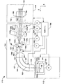
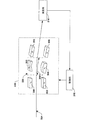
- イオンビームを生成するように構成されているイオンビーム源と、
生成された上記イオンビームを質量分析するための質量分析部と、
上記質量分析部の下流側に設置されている偏向部であって、質量分析された上記イオンビームを偏向するための偏向領域を有している偏向部と、
上記偏向部の下流側に設置されているエンドステーションであって、上記イオンビームによりイオンを注入されるワークピースを支持するように構成されているエンドステーションと、
を備えており、
上記偏向部は、上記偏向領域の長さを変更するように構成されている、
ことを特徴とするイオン注入システム。 - 上記偏向部は、
第一電極と、
上記第一電極との間に間隙を有する第二電極と、
上記第一電極および上記第二電極の少なくとも一つに電圧を印加するためのバイアス要素と、
を備えており、
上記間隙を飛行する上記イオンビームのイオンを偏向するように上記第一電極と上記第二電極との間に電場が生成され、
上記第一電極および上記第二電極の少なくとも一つが、上記イオンビームの飛行パスに沿って複数の電極セグメントを形成するように細分化され、
上記電極セグメントの各々が、上記偏向部の長さを選択的に制御するように個別にバイアスされる、
ことを特徴とする請求項1に記載のイオン注入システム。 - 複数の上記電極セグメントのうち一または複数の該電極セグメントが、電極間隙を挟んで対向する上部電極および下部電極を備えており、
上部電極は、少なくとも3つのセグメントに細分化されており、下部電極は、少なくとも3つのセグメントに細分化されている、
ことを特徴とする請求項2に記載のイオン注入システム。 - 上部電極および下部電極の最初のセグメントおよび最後のセグメントが、該上部電極の該最初のセグメントと該下部電極の該最初のセグメントとの間にある該間隙、および、該上部電極の該最後のセグメントと該下部電極の該最後のセグメントとの間にある該間隙において、周辺よりも負の電位分布を生じさせるようにバイアスされる、
ことを特徴とする請求項2に記載のイオン注入システム。 - 上記上部電極の最初の電極セグメントと最後の電極セグメントとの間にある少なくとも一つの電極セグメントが正にバイアスされ、上記下部電極の最初の電極セグメントと最後の電極セグメントとの間にある少なくとも一つの電極セグメントが、該上部電極のそれぞれのセグメントよりも負にバイアスされる、
ことを特徴とする請求項3に記載のイオン注入システム。 - 上記下部電極の中間セグメントが負にバイアスされ、残りのセグメントおよび上記上部電極の電位が、上記偏向部における上記偏向領域の長さを最小限にするように、周辺に関してグラウンドである、
ことを特徴とする請求項3に記載のイオン注入システム。 - 一または複数のイオンビームの特性を測定するように構成されている測定部と、
上記測定部、上記イオンビーム源、上記質量分析部、および上記偏向部と機能的に接続されており、上記測定部により取得された測定値に応じて、上記イオンビーム源、上記質量分析部、および上記偏向部の少なくとも一つの動作を調整するように構成されている制御部と、
を更に備えており、
上記イオンビームの特性は、該イオンビームの電圧、電流、質量、電荷、エネルギー、および種の少なくとも一つを含んでいる、
ことを特徴とする請求項1に記載のイオン注入システム。 - 汚染物質をフィルタアウトするように上記イオンビームを略S字型に湾曲させると共に、上記イオンビームを、それぞれが略等しい実効長を有する複数の平行ビームレットに平行化する平行化部
を更に備えている、
ことを特徴とする請求項1に記載のイオン注入システム。 - 上記イオンビームは、上記偏向部により偏向されると共に、上記偏向部により減速、集束、または減速および集束される、
ことを特徴とする請求項1に記載のイオン注入システム。 - 一または複数のイオンビームの特性を測定するように構成されている測定部と、
上記測定部、および、上記測定部により取得された測定値に応じて上記イオンビームを加速または減速させるフォーカシングレンズに機能的に接続されている制御部と、
を更に備えている、
ことを特徴とする請求項1に記載のイオン注入システム。 - イオン注入システムにおけるビームラインにおいて用いられる電気的偏向装置であって、
イオンビームを偏向可能な偏向領域を有する電気的偏向部、
を備えており、
上記電気的偏向部は、上記偏向領域の長さを変更するように構成されている、
ことを特徴とする電気的偏向装置。 - 上記電気的偏向部は、
第一電極と、
上記第一電極との間に間隙を有する第二電極と、
上記第一電極および上記第二電極の少なくとも一つに電圧を印加するためのバイアス要素と、
を備えており、
上記間隙を飛行する上記イオンビームのイオンを偏向するように上記第一電極と上記第二電極との間に電場が生成され、
上記第一電極および上記第二電極の少なくとも一つが、上記イオンビームの飛行パスに沿って複数の電極セグメントを形成するように細分化され、
上記電極セグメントのそれぞれが、上記偏向部の長さを選択的に制御するように個別にバイアスされる、
ことを特徴とする請求項11に記載の電気的偏向装置。 - 一または複数のイオンビームの特性を測定するように構成されている測定部と、
上記測定部および上記電気的偏向部に機能的に接続されており、上記偏向領域の長さを選択的に制御するように電極セグメントの各々に個別にバイアスをかけることにより、上記測定部により取得された測定値に応じて、該電気的偏向部の動作を調整するように構成されている制御部と、
を備えており、
上記測定部により測定されたビームの特性は、上記イオンビームの電圧、電流、質量、電荷、エネルギー、および、種の少なくとも一つを含んでいる、
ことを特徴とする請求項12に記載の電気的偏向装置。 - 上記イオンビームが、上記電気的偏向部により偏向されると共に、該偏向部により減速、集束、または減速及び集束される、
ことを特徴とする請求項11に記載の電気的偏向装置。 - 複数の上記電極セグメントのうち一または複数の該電極セグメントが、電極間隙を挟んで対向する上部電極および下部電極を備えており、
上部電極は、少なくとも3つのセグメントに細分化されており、下部電極は、少なくとも3つのセグメントに細分化されている、
ことを特徴とする請求項12に記載の電気的偏向装置。 - イオン注入システムにおいて、ワークピースにイオンを注入する方法であって、
上記イオン注入システムにおいて、イオンビームを生成するステップと、
上記イオンビームの一または複数のビーム特性を測定するステップと、
ビーム特性に基づいて、上記イオン注入システムにおける偏向部の間隙の中間にある一または複数の電極に印加されるそれぞれのバイアス電圧を選択的に調整することにより、該イオン注入システムにおける該偏向部を飛行する上記イオンビームの実効長を変化させるステップと、
を含んでいることを特徴とする方法。 - バイアス電圧が、上記イオンビームを偏向するように、上記偏向部における1組、2組、または3組の電極に印加されるべきか否かを判定するステップ、
を更に含んでいることを特徴とする請求項16に記載の方法。 - 上記偏向部の上記実効長を選択的に制御するステップ、
を更に含んでいることを特徴とする請求項16に記載の方法。 - 上記イオンビームの収束、加速、または減速の少なくとも一つを制御するように、上記偏向部の第一電極および第二電極に印加されるそれぞれのバイアス電圧を選択的に調整するステップ、
を更に含んでいることを特徴とする請求項16に記載の方法。 - 上記イオンビームの、エネルギー、電流、および種の少なくとも一つに基づいて偏向を制御するように、上記偏向部の第一電極および第二電極に印加されるそれぞれのバイアス電圧を選択的に調整するステップ、
を更に含んでいることを特徴とする請求項16に記載の方法。
Applications Claiming Priority (3)
| Application Number | Priority Date | Filing Date | Title |
|---|---|---|---|
| US12/212,507 US20100065761A1 (en) | 2008-09-17 | 2008-09-17 | Adjustable deflection optics for ion implantation |
| US12/212,507 | 2008-09-17 | ||
| PCT/US2009/005182 WO2010033199A1 (en) | 2008-09-17 | 2009-09-17 | Adjustable deflection optics for ion implantation |
Publications (2)
| Publication Number | Publication Date |
|---|---|
| JP2012503295A true JP2012503295A (ja) | 2012-02-02 |
| JP5739333B2 JP5739333B2 (ja) | 2015-06-24 |
Family
ID=41559628
Family Applications (1)
| Application Number | Title | Priority Date | Filing Date |
|---|---|---|---|
| JP2011527819A Active JP5739333B2 (ja) | 2008-09-17 | 2009-09-17 | イオン注入に用いる調整可能な偏向光学 |
Country Status (7)
| Country | Link |
|---|---|
| US (1) | US20100065761A1 (ja) |
| EP (1) | EP2340549A1 (ja) |
| JP (1) | JP5739333B2 (ja) |
| KR (1) | KR20110081980A (ja) |
| CN (1) | CN102160139A (ja) |
| TW (1) | TWI486992B (ja) |
| WO (1) | WO2010033199A1 (ja) |
Cited By (3)
| Publication number | Priority date | Publication date | Assignee | Title |
|---|---|---|---|---|
| CN104952681A (zh) * | 2014-03-27 | 2015-09-30 | 斯伊恩股份有限公司 | 离子注入装置、最终能量过滤器以及离子注入方法 |
| JP2017041441A (ja) * | 2015-08-20 | 2017-02-23 | 日新イオン機器株式会社 | イオン注入システム |
| JP2017510023A (ja) * | 2014-01-15 | 2017-04-06 | アクセリス テクノロジーズ, インコーポレイテッド | 可変エネルギー制御を伴うイオン注入システムおよび方法 |
Families Citing this family (19)
| Publication number | Priority date | Publication date | Assignee | Title |
|---|---|---|---|---|
| US7767986B2 (en) * | 2008-06-20 | 2010-08-03 | Varian Semiconductor Equipment Associates, Inc. | Method and apparatus for controlling beam current uniformity in an ion implanter |
| US8519353B2 (en) | 2010-12-29 | 2013-08-27 | Varian Semiconductor Equipment Associates, Inc. | Method and apparatus for controlling an asymmetric electrostatic lens about a central ray trajectory of an ion beam |
| CN103094032B (zh) * | 2011-11-07 | 2016-08-10 | 北京中科信电子装备有限公司 | 一种多电极束流聚焦调节装置 |
| US8637838B2 (en) * | 2011-12-13 | 2014-01-28 | Axcelis Technologies, Inc. | System and method for ion implantation with improved productivity and uniformity |
| US9502213B2 (en) * | 2013-03-15 | 2016-11-22 | Nissin Ion Equipment Co., Ltd. | Ion beam line |
| US8835879B1 (en) * | 2013-06-03 | 2014-09-16 | Varian Semiconductor Equipment Associates, Inc. | Reduction of deposition by separation of ion beam and neutral flow |
| US20150228445A1 (en) * | 2014-02-13 | 2015-08-13 | Varian Semiconductor Equipment Associates, Inc. | Method and apparatus for three dimensional ion implantation |
| US9455116B2 (en) | 2014-04-30 | 2016-09-27 | Axcells Technologies, Inc. | Angular scanning using angular energy filter |
| TWI501286B (zh) * | 2014-06-27 | 2015-09-21 | Advanced Ion Beam Tech Inc | 離子佈植機 |
| TWI523084B (zh) | 2014-11-11 | 2016-02-21 | 漢辰科技股份有限公司 | 離子佈植法 |
| US9679739B2 (en) * | 2014-12-26 | 2017-06-13 | Axcelis Technologies, Inc. | Combined electrostatic lens system for ion implantation |
| TWI795448B (zh) | 2017-10-09 | 2023-03-11 | 美商艾克塞利斯科技公司 | 用於在角能量過濾器區域中穩定或移除射束線組件上所形成之膜的離子植入系統及方法 |
| JP7040199B2 (ja) * | 2018-03-26 | 2022-03-23 | 株式会社島津製作所 | 荷電粒子ビーム軸合わせ装置、荷電粒子ビーム照射装置および荷電粒子ビーム軸合わせ方法 |
| US10886098B2 (en) | 2018-11-20 | 2021-01-05 | Applied Materials, Inc. | Electrostatic filter and ion implanter having asymmetric electrostatic configuration |
| US10804068B2 (en) | 2018-11-20 | 2020-10-13 | Applied Materials, Inc. | Electostatic filter and method for controlling ion beam properties using electrostatic filter |
| US10790116B2 (en) | 2018-11-20 | 2020-09-29 | Applied Materials, Inc. | Electostatic filter and method for controlling ion beam using electostatic filter |
| US10937624B2 (en) | 2018-11-20 | 2021-03-02 | Applied Materials, Inc. | Apparatus and method for controlling ion beam using electrostatic filter |
| US11646175B2 (en) | 2019-02-15 | 2023-05-09 | Axcelis Technologies, Inc. | Method of mixing upstream and downstream current measurements for inference of the beam current at the bend of an optical element for realtime dose control |
| US11217427B1 (en) * | 2020-11-27 | 2022-01-04 | Applied Materials, Inc. | System, apparatus and method for bunched ribbon ion beam |
Citations (4)
| Publication number | Priority date | Publication date | Assignee | Title |
|---|---|---|---|---|
| JPS61233955A (ja) * | 1985-03-08 | 1986-10-18 | Nissin Electric Co Ltd | イオン注入装置 |
| WO2002052609A2 (en) * | 2000-12-27 | 2002-07-04 | Proteros, Llc | Compact beamline and ion implanter system using same |
| JP2005190979A (ja) * | 2003-12-04 | 2005-07-14 | Nissin Ion Equipment Co Ltd | イオンビーム装置 |
| WO2008042094A2 (en) * | 2006-09-29 | 2008-04-10 | Axcelis Technologies, Inc. | New and improved beam line architecture for ion implanter |
Family Cites Families (28)
| Publication number | Priority date | Publication date | Assignee | Title |
|---|---|---|---|---|
| US4593200A (en) * | 1984-03-06 | 1986-06-03 | Mcguire Iii Edward L | Scan controller for ion implanter device |
| US4980562A (en) * | 1986-04-09 | 1990-12-25 | Varian Associates, Inc. | Method and apparatus for high efficiency scanning in an ion implanter |
| US4736107A (en) * | 1986-09-24 | 1988-04-05 | Eaton Corporation | Ion beam implanter scan control system |
| US5311028A (en) * | 1990-08-29 | 1994-05-10 | Nissin Electric Co., Ltd. | System and method for producing oscillating magnetic fields in working gaps useful for irradiating a surface with atomic and molecular ions |
| US5160846A (en) * | 1990-10-03 | 1992-11-03 | Eaton Corporation | Method and apparatus for reducing tilt angle variations in an ion implanter |
| US5270222A (en) * | 1990-12-31 | 1993-12-14 | Texas Instruments Incorporated | Method and apparatus for semiconductor device fabrication diagnosis and prognosis |
| US5293216A (en) * | 1990-12-31 | 1994-03-08 | Texas Instruments Incorporated | Sensor for semiconductor device manufacturing process control |
| US5177366A (en) * | 1992-03-06 | 1993-01-05 | Eaton Corporation | Ion beam implanter for providing cross plane focusing |
| US5432352A (en) * | 1993-09-20 | 1995-07-11 | Eaton Corporation | Ion beam scan control |
| US5481116A (en) * | 1994-06-10 | 1996-01-02 | Ibis Technology Corporation | Magnetic system and method for uniformly scanning heavy ion beams |
| US6137112A (en) * | 1998-09-10 | 2000-10-24 | Eaton Corporation | Time of flight energy measurement apparatus for an ion beam implanter |
| US6521895B1 (en) * | 1999-10-22 | 2003-02-18 | Varian Semiconductor Equipment Associates, Inc. | Wide dynamic range ion beam scanners |
| JP3414337B2 (ja) * | 1999-11-12 | 2003-06-09 | 日新電機株式会社 | 電磁界レンズの制御方法およびイオン注入装置 |
| US6414329B1 (en) * | 2000-07-25 | 2002-07-02 | Axcelis Technologies, Inc. | Method and system for microwave excitation of plasma in an ion beam guide |
| US6534775B1 (en) * | 2000-09-01 | 2003-03-18 | Axcelis Technologies, Inc. | Electrostatic trap for particles entrained in an ion beam |
| US6908836B2 (en) * | 2002-09-23 | 2005-06-21 | Applied Materials, Inc. | Method of implanting a substrate and an ion implanter for performing the method |
| US20030197133A1 (en) * | 2002-04-23 | 2003-10-23 | Turner Norman L. | Method and apparatus for scanning a workpiece in a vacuum chamber |
| US6924215B2 (en) * | 2002-05-29 | 2005-08-02 | Taiwan Semiconductor Manufacturing Co., Ltd | Method of monitoring high tilt angle of medium current implant |
| KR20040060401A (ko) * | 2002-12-30 | 2004-07-06 | 주식회사 하이닉스반도체 | 반도체소자의 트랜지스터 형성 방법 |
| US6777696B1 (en) * | 2003-02-21 | 2004-08-17 | Axcelis Technologies, Inc. | Deflecting acceleration/deceleration gap |
| US6881966B2 (en) * | 2003-05-15 | 2005-04-19 | Axcelis Technologies, Inc. | Hybrid magnetic/electrostatic deflector for ion implantation systems |
| US7112809B2 (en) * | 2003-06-26 | 2006-09-26 | Axcelis Technologies, Inc. | Electrostatic lens for ion beams |
| US6774377B1 (en) * | 2003-06-26 | 2004-08-10 | Axcelis Technologies, Inc. | Electrostatic parallelizing lens for ion beams |
| US6972236B2 (en) * | 2004-01-30 | 2005-12-06 | Chartered Semiconductor Manufacturing Ltd. | Semiconductor device layout and channeling implant process |
| US7462843B2 (en) * | 2004-05-18 | 2008-12-09 | Advanced Ion Bean Technology Inc. | Apparatus and methods for ion beam implantation |
| US7326941B2 (en) * | 2004-05-18 | 2008-02-05 | Advanced Ion Beam Technology, Inc. | Apparatus and methods for ion beam implantation using ribbon and spot beams |
| US6992310B1 (en) * | 2004-08-13 | 2006-01-31 | Axcelis Technologies, Inc. | Scanning systems and methods for providing ions from an ion beam to a workpiece |
| JP4600426B2 (ja) * | 2006-06-26 | 2010-12-15 | 日新イオン機器株式会社 | イオン注入装置およびイオンビームの偏差角補正方法 |
-
2008
- 2008-09-17 US US12/212,507 patent/US20100065761A1/en not_active Abandoned
-
2009
- 2009-09-17 WO PCT/US2009/005182 patent/WO2010033199A1/en active Application Filing
- 2009-09-17 JP JP2011527819A patent/JP5739333B2/ja active Active
- 2009-09-17 TW TW098131340A patent/TWI486992B/zh active
- 2009-09-17 KR KR1020117008677A patent/KR20110081980A/ko not_active Application Discontinuation
- 2009-09-17 EP EP09745145A patent/EP2340549A1/en not_active Withdrawn
- 2009-09-17 CN CN2009801363813A patent/CN102160139A/zh active Pending
Patent Citations (4)
| Publication number | Priority date | Publication date | Assignee | Title |
|---|---|---|---|---|
| JPS61233955A (ja) * | 1985-03-08 | 1986-10-18 | Nissin Electric Co Ltd | イオン注入装置 |
| WO2002052609A2 (en) * | 2000-12-27 | 2002-07-04 | Proteros, Llc | Compact beamline and ion implanter system using same |
| JP2005190979A (ja) * | 2003-12-04 | 2005-07-14 | Nissin Ion Equipment Co Ltd | イオンビーム装置 |
| WO2008042094A2 (en) * | 2006-09-29 | 2008-04-10 | Axcelis Technologies, Inc. | New and improved beam line architecture for ion implanter |
Cited By (8)
| Publication number | Priority date | Publication date | Assignee | Title |
|---|---|---|---|---|
| JP2017510023A (ja) * | 2014-01-15 | 2017-04-06 | アクセリス テクノロジーズ, インコーポレイテッド | 可変エネルギー制御を伴うイオン注入システムおよび方法 |
| CN104952681A (zh) * | 2014-03-27 | 2015-09-30 | 斯伊恩股份有限公司 | 离子注入装置、最终能量过滤器以及离子注入方法 |
| KR20150112785A (ko) * | 2014-03-27 | 2015-10-07 | 스미도모쥬기가이 이온 테크놀로지 가부시키가이샤 | 이온주입장치, 최종에너지필터, 및 이온주입방법 |
| JP2015191740A (ja) * | 2014-03-27 | 2015-11-02 | 住友重機械イオンテクノロジー株式会社 | イオン注入装置、最終エネルギーフィルター、及びイオン注入方法 |
| US9293295B2 (en) | 2014-03-27 | 2016-03-22 | Sumitomo Heavy Industries Ion Technology Co., Ltd. | Ion implantation apparatus, final energy filter, and ion implantation method |
| CN104952681B (zh) * | 2014-03-27 | 2018-06-19 | 斯伊恩股份有限公司 | 离子注入装置、最终能量过滤器以及离子注入方法 |
| KR102342019B1 (ko) * | 2014-03-27 | 2021-12-22 | 스미도모쥬기가이 이온 테크놀로지 가부시키가이샤 | 이온주입장치, 최종에너지필터, 및 이온주입방법 |
| JP2017041441A (ja) * | 2015-08-20 | 2017-02-23 | 日新イオン機器株式会社 | イオン注入システム |
Also Published As
| Publication number | Publication date |
|---|---|
| WO2010033199A1 (en) | 2010-03-25 |
| US20100065761A1 (en) | 2010-03-18 |
| CN102160139A (zh) | 2011-08-17 |
| EP2340549A1 (en) | 2011-07-06 |
| JP5739333B2 (ja) | 2015-06-24 |
| TW201027586A (en) | 2010-07-16 |
| TWI486992B (zh) | 2015-06-01 |
| KR20110081980A (ko) | 2011-07-15 |
Similar Documents
| Publication | Publication Date | Title |
|---|---|---|
| JP5739333B2 (ja) | イオン注入に用いる調整可能な偏向光学 | |
| JP5652583B2 (ja) | ハイブリッド結合及び二重機械式走査構造を有するイオン注入システム及び方法 | |
| JP5323705B2 (ja) | イオン注入器のための改良型新規ビームラインアーキテクチャ | |
| JP6169098B2 (ja) | 生産性および均一性が向上したイオン注入システムおよび方法 | |
| US7615763B2 (en) | System for magnetic scanning and correction of an ion beam | |
| JP2010503964A (ja) | イオン注入装置におけるビーム角調整システムおよびその調整方法 | |
| KR101828633B1 (ko) | 리본 이온빔의 에너지 변경 시스템 및 이온 주입 시스템 | |
| US20180068828A1 (en) | In situ beam current monitoring and control in scanned ion implantation systems | |
| KR101653731B1 (ko) | 빔 상보성 개구 형상을 빔 형상에 맞춤으로써 오염 및 미립자를 감소시키기 위한 시스템 및 방법 | |
| EP1721329A2 (en) | Modulating ion beam current | |
| KR102342213B1 (ko) | 이온주입장치 | |
| JP2017539062A (ja) | ビーム減速を伴うイオン注入器におけるビーム角度調整のためのシステムおよび方法 | |
| JP7154236B2 (ja) | イオン注入システムにおける注入角度を補正するための方法、およびイオン注入システム | |
| JP5517016B2 (ja) | ウインドウフレーム磁石アッセンブリ及びイオンビームを質量分析する方法 | |
| JP2018170086A (ja) | イオン注入装置及びイオン注入方法 | |
| US11049691B2 (en) | Ion beam quality control using a movable mass resolving device |
Legal Events
| Date | Code | Title | Description |
|---|---|---|---|
| A621 | Written request for application examination |
Free format text: JAPANESE INTERMEDIATE CODE: A621 Effective date: 20120817 |
|
| A977 | Report on retrieval |
Free format text: JAPANESE INTERMEDIATE CODE: A971007 Effective date: 20131127 |
|
| A131 | Notification of reasons for refusal |
Free format text: JAPANESE INTERMEDIATE CODE: A131 Effective date: 20131210 |
|
| A521 | Request for written amendment filed |
Free format text: JAPANESE INTERMEDIATE CODE: A523 Effective date: 20140304 |
|
| A131 | Notification of reasons for refusal |
Free format text: JAPANESE INTERMEDIATE CODE: A131 Effective date: 20140520 |
|
| A601 | Written request for extension of time |
Free format text: JAPANESE INTERMEDIATE CODE: A601 Effective date: 20140820 |
|
| A602 | Written permission of extension of time |
Free format text: JAPANESE INTERMEDIATE CODE: A602 Effective date: 20140827 |
|
| A521 | Request for written amendment filed |
Free format text: JAPANESE INTERMEDIATE CODE: A523 Effective date: 20141120 |
|
| TRDD | Decision of grant or rejection written | ||
| A01 | Written decision to grant a patent or to grant a registration (utility model) |
Free format text: JAPANESE INTERMEDIATE CODE: A01 Effective date: 20150324 |
|
| A61 | First payment of annual fees (during grant procedure) |
Free format text: JAPANESE INTERMEDIATE CODE: A61 Effective date: 20150423 |
|
| R150 | Certificate of patent or registration of utility model |
Ref document number: 5739333 Country of ref document: JP Free format text: JAPANESE INTERMEDIATE CODE: R150 |
|
| R250 | Receipt of annual fees |
Free format text: JAPANESE INTERMEDIATE CODE: R250 |
|
| R250 | Receipt of annual fees |
Free format text: JAPANESE INTERMEDIATE CODE: R250 |
|
| R250 | Receipt of annual fees |
Free format text: JAPANESE INTERMEDIATE CODE: R250 |
|
| R250 | Receipt of annual fees |
Free format text: JAPANESE INTERMEDIATE CODE: R250 |
|
| R250 | Receipt of annual fees |
Free format text: JAPANESE INTERMEDIATE CODE: R250 |
|
| R250 | Receipt of annual fees |
Free format text: JAPANESE INTERMEDIATE CODE: R250 |