JP2012253091A - Photovoltaic device and method for manufacturing the same - Google Patents
Photovoltaic device and method for manufacturing the same Download PDFInfo
- Publication number
- JP2012253091A JP2012253091A JP2011122665A JP2011122665A JP2012253091A JP 2012253091 A JP2012253091 A JP 2012253091A JP 2011122665 A JP2011122665 A JP 2011122665A JP 2011122665 A JP2011122665 A JP 2011122665A JP 2012253091 A JP2012253091 A JP 2012253091A
- Authority
- JP
- Japan
- Prior art keywords
- semiconductor layer
- heat treatment
- intrinsic
- photovoltaic device
- type amorphous
- Prior art date
- Legal status (The legal status is an assumption and is not a legal conclusion. Google has not performed a legal analysis and makes no representation as to the accuracy of the status listed.)
- Withdrawn
Links
Images

Classifications
-
- Y—GENERAL TAGGING OF NEW TECHNOLOGICAL DEVELOPMENTS; GENERAL TAGGING OF CROSS-SECTIONAL TECHNOLOGIES SPANNING OVER SEVERAL SECTIONS OF THE IPC; TECHNICAL SUBJECTS COVERED BY FORMER USPC CROSS-REFERENCE ART COLLECTIONS [XRACs] AND DIGESTS
- Y02—TECHNOLOGIES OR APPLICATIONS FOR MITIGATION OR ADAPTATION AGAINST CLIMATE CHANGE
- Y02E—REDUCTION OF GREENHOUSE GAS [GHG] EMISSIONS, RELATED TO ENERGY GENERATION, TRANSMISSION OR DISTRIBUTION
- Y02E10/00—Energy generation through renewable energy sources
- Y02E10/50—Photovoltaic [PV] energy
- Y02E10/547—Monocrystalline silicon PV cells
-
- Y—GENERAL TAGGING OF NEW TECHNOLOGICAL DEVELOPMENTS; GENERAL TAGGING OF CROSS-SECTIONAL TECHNOLOGIES SPANNING OVER SEVERAL SECTIONS OF THE IPC; TECHNICAL SUBJECTS COVERED BY FORMER USPC CROSS-REFERENCE ART COLLECTIONS [XRACs] AND DIGESTS
- Y02—TECHNOLOGIES OR APPLICATIONS FOR MITIGATION OR ADAPTATION AGAINST CLIMATE CHANGE
- Y02E—REDUCTION OF GREENHOUSE GAS [GHG] EMISSIONS, RELATED TO ENERGY GENERATION, TRANSMISSION OR DISTRIBUTION
- Y02E10/00—Energy generation through renewable energy sources
- Y02E10/50—Photovoltaic [PV] energy
- Y02E10/548—Amorphous silicon PV cells
Abstract
Description
この発明は、太陽電池などの光起電力装置及びその製造方法に関するものであり、特に結晶シリコン系太陽電池において高効率化が可能なヘテロ接合太陽電池及びその製造方法に関するものである。 The present invention relates to a photovoltaic device such as a solar cell and a method for manufacturing the same, and more particularly to a heterojunction solar cell capable of increasing efficiency in a crystalline silicon solar cell and a method for manufacturing the same.
近年、結晶シリコン基板を用いた光起電力装置として、非晶質半導体薄膜を組み合わせたヘテロ接合構造を有するヘテロ接合太陽電池の開発が盛んに行われている。特許文献1〜3において、結晶シリコン基板に薄い真性半導体層を介して不純物ドープシリコン層からなるPN接合或いはBSF層を形成するヘテロ接合太陽電池に関する発明が記載されている。不純物ドープ層を薄膜で形成することにより不純物ドープ層の濃度分布を自由に設定でき、また、間に挿入した真性半導体層は接合間の不純物拡散を抑制し、急峻な不純物プロファイルをもつ接合を形成することができるため、良好な接合界面形成により高い開放電圧を得ることができる。さらに真性半導体層、不純物ドープ層は200℃程度の低温で形成できるため、基板の厚みが薄くても熱により基板に生じるストレスや、基板の反りを低減することができ、また、高温プロセスで顕在化する結晶基板内の酸素誘起積層欠陥の影響も大きく低減される。 In recent years, as a photovoltaic device using a crystalline silicon substrate, a heterojunction solar cell having a heterojunction structure combined with an amorphous semiconductor thin film has been actively developed. Patent Documents 1 to 3 describe an invention relating to a heterojunction solar cell in which a PN junction or a BSF layer made of an impurity-doped silicon layer is formed on a crystalline silicon substrate via a thin intrinsic semiconductor layer. By forming the impurity doped layer as a thin film, the concentration distribution of the impurity doped layer can be freely set, and the intrinsic semiconductor layer inserted between them suppresses impurity diffusion between junctions and forms a junction with a steep impurity profile Therefore, a high open circuit voltage can be obtained by forming a good bonding interface. Furthermore, since the intrinsic semiconductor layer and the impurity doped layer can be formed at a low temperature of about 200 ° C., the stress generated on the substrate due to heat and the warpage of the substrate can be reduced even when the substrate is thin, and it is manifested by a high temperature process. The influence of oxygen-induced stacking faults in the crystal substrate to be converted is greatly reduced.
ヘテロ接合太陽電池の変換効率を向上させる方法として、特許文献4では、結晶シリコン基板と真性半導体層との界面欠陥密度を低減させてキャリア再結合を抑制するために、結晶シリコン基板と真性半導体層との界面近傍の酸素濃度を高くした構造が開示されている。また、特許文献5では、基板側の真性半導体層の酸素濃度を、不純物ドープ層側の真性半導体層の酸素濃度より低くした構造が開示されている。結晶シリコン基板側の酸素濃度を低くして酸素起因の欠陥を少なくすることでキャリアの再結合を抑制すると同時に、不純物ドープ層側においては酸素濃度を高めてn型の性質を持たせることでp型非晶質半導体層と真性半導体層の界面近傍の内蔵電界を強くしキャリア分離の効果を高めている。 As a method for improving the conversion efficiency of a heterojunction solar cell, in Patent Document 4, in order to reduce the interface defect density between the crystalline silicon substrate and the intrinsic semiconductor layer and suppress carrier recombination, the crystalline silicon substrate and the intrinsic semiconductor layer A structure in which the oxygen concentration in the vicinity of the interface is increased is disclosed. Patent Document 5 discloses a structure in which the oxygen concentration of the intrinsic semiconductor layer on the substrate side is lower than the oxygen concentration of the intrinsic semiconductor layer on the impurity doped layer side. By reducing the oxygen concentration on the crystalline silicon substrate side to reduce oxygen-induced defects, the recombination of carriers is suppressed, and at the same time, the oxygen concentration is increased on the impurity doped layer side to give n-type properties. The built-in electric field in the vicinity of the interface between the type amorphous semiconductor layer and the intrinsic semiconductor layer is strengthened to enhance the effect of carrier separation.
上記特許文献4では、結晶シリコン基板と真性半導体層界面近傍の酸素濃度についてのみ言及されているが、真性半導体層のそれ以外の部分については検討されていない。また、結晶シリコン基板、非晶質半導体層、電極の各界面特性を向上させる熱処理についても検討されていない。 In the above-mentioned Patent Document 4, only the oxygen concentration in the vicinity of the interface between the crystalline silicon substrate and the intrinsic semiconductor layer is mentioned, but other portions of the intrinsic semiconductor layer are not examined. Further, heat treatment for improving the interface characteristics of the crystalline silicon substrate, the amorphous semiconductor layer, and the electrode has not been studied.
また、上記特許文献5では、真性半導体層の結晶シリコン基板側の酸素濃度が不純物ドープ層側と比べて低く、界面特性を向上させる熱処理を施した場合にその効果が十分得ることができないといった問題がある。また、結晶シリコン基板、非晶質半導体層、電極の各界面特性を向上させる熱処理についても検討されていない。また、この構成において、電極形成後に熱処理を行っても光起電力装置の出力特性が十分に得られない問題があった。 Further, in Patent Document 5, the oxygen concentration on the crystalline silicon substrate side of the intrinsic semiconductor layer is lower than that on the impurity doped layer side, and the effect cannot be sufficiently obtained when heat treatment for improving the interface characteristics is performed. There is. Further, heat treatment for improving the interface characteristics of the crystalline silicon substrate, the amorphous semiconductor layer, and the electrode has not been studied. Further, in this configuration, there is a problem that the output characteristics of the photovoltaic device cannot be sufficiently obtained even if heat treatment is performed after the electrodes are formed.
本発明は、上記に鑑みてなされたものであって、従来方法と比べて出力特性を向上させることができる光起電力装置及びその製造方法を提供することを目的とする。 The present invention has been made in view of the above, and an object of the present invention is to provide a photovoltaic device capable of improving output characteristics as compared with a conventional method and a method for manufacturing the photovoltaic device.
上述した課題を解決し、目的を達成するために、本発明の光起電力装置及びその製造方法は、第一導電型結晶系半導体基板と、第一導電型結晶系半導体基板の第一面上に基板側から、真性な非晶質半導体層、第二導電型非晶質半導体層の順で形成された各層と、第一導電型結晶系半導体基板の第一面と反対側の第二面上に形成された第一導電型非晶質半導体層を有し、真性な非晶質半導体層は、基板側から積層された第一の酸素濃度の第一真性半導体層と、第一の酸素濃度より低い第二の酸素濃度の第二真性半導体層とから構成される光起電力装置において、第一真性半導体層は、第一の形成温度にて形成の後、第一の形成温度より高い第一の熱処理温度で熱処理され、第二真性半導体層、第二導電型非晶質半導体層、および第一導電型非晶質半導体層は、第一の形成温度以下の第二の形成温度で形成されていることを特徴とする。 In order to solve the above-described problems and achieve the object, a photovoltaic device and a manufacturing method thereof according to the present invention are provided on a first conductive crystal semiconductor substrate and a first surface of the first conductive crystal semiconductor substrate. Each layer formed in this order from the substrate side to the intrinsic amorphous semiconductor layer, the second conductive type amorphous semiconductor layer, and the second side opposite to the first side of the first conductive type crystalline semiconductor substrate The intrinsic amorphous semiconductor layer having the first conductive type amorphous semiconductor layer formed thereon includes a first intrinsic semiconductor layer having a first oxygen concentration stacked from the substrate side, and a first oxygen semiconductor layer. In a photovoltaic device comprising a second intrinsic semiconductor layer having a second oxygen concentration lower than the concentration, the first intrinsic semiconductor layer is higher than the first formation temperature after being formed at the first formation temperature. Heat-treated at the first heat treatment temperature, second intrinsic semiconductor layer, second conductive type amorphous semiconductor layer, and first conductive type amorphous The semiconductor layer is characterized in that it is formed by the following first forming temperature second forming temperature.
上述した課題を解決し、目的を達成するために、本発明の光起電力装置及びその製造方法は、第一導電型結晶系半導体基板と、第一導電型結晶系半導体基板の第一面上に基板側から、真性な非晶質半導体層、第二導電型非晶質半導体層の順で形成された各層と、第一導電型結晶系半導体基板の第一面と反対側の第二面上に形成された第一導電型非晶質半導体層を有し、真性な非晶質半導体層は、基板側から積層された第一の酸素濃度の第一真性半導体層と、第一の酸素濃度より低い第二の酸素濃度の第二真性半導体層とから構成される光起電力装置の製造方法において、第一の形成温度にて第一真性半導体層を形成の後、第一真性半導体層を第一の形成温度より高い第一の熱処理温度で熱処理すると共に、第一の形成温度以下の第二の形成温度で、第二真性半導体層、第二導電型非晶質半導体層、および第一導電型非晶質半導体層を形成することを特徴とする。 In order to solve the above-described problems and achieve the object, a photovoltaic device and a manufacturing method thereof according to the present invention are provided on a first conductive crystal semiconductor substrate and a first surface of the first conductive crystal semiconductor substrate. Each layer formed in this order from the substrate side to the intrinsic amorphous semiconductor layer, the second conductive type amorphous semiconductor layer, and the second side opposite to the first side of the first conductive type crystalline semiconductor substrate The intrinsic amorphous semiconductor layer having the first conductive type amorphous semiconductor layer formed thereon includes a first intrinsic semiconductor layer having a first oxygen concentration stacked from the substrate side, and a first oxygen semiconductor layer. In a method for manufacturing a photovoltaic device comprising a second intrinsic semiconductor layer having a second oxygen concentration lower than the concentration, after forming the first intrinsic semiconductor layer at a first formation temperature, the first intrinsic semiconductor layer Heat treatment at a first heat treatment temperature higher than the first formation temperature and a second formation temperature not higher than the first formation temperature. In the second intrinsic semiconductor layer, and forming a second conductive type amorphous semiconductor layer, and the first conductive type amorphous semiconductor layer.
また、上記第一の熱処理温度は、上記第一の形成温度より5〜200℃高くされ、より好ましくは10〜150℃高いほうがよく、絶対温度では400℃以下にするのが好ましい。400℃より高くなると、酸素を含有する第一真性半導体層の水素脱離による膜質の劣化が顕著になり、光起電力装置の出力が低下するからである。熱処理時間は、上記第一の熱処理温度と反比例し、1〜120分間程度、5〜60分間がより好ましい。 The first heat treatment temperature is higher by 5 to 200 ° C., more preferably 10 to 150 ° C. higher than the first formation temperature, and is preferably 400 ° C. or lower in absolute temperature. This is because when the temperature is higher than 400 ° C., the deterioration of the film quality due to the hydrogen desorption of the first intrinsic semiconductor layer containing oxygen becomes remarkable, and the output of the photovoltaic device decreases. The heat treatment time is inversely proportional to the first heat treatment temperature and is preferably about 1 to 120 minutes and more preferably 5 to 60 minutes.
第一真性半導体層形成後に、第一真性半導体層の第一の形成温度より高い第一の熱処理温度で熱処理すると共に、第一の形成温度以下の温度で、第二真性半導体層、第二導電型非晶質半導体層、そして第一導電型非晶質半導体層を形成することにより、CVD(Chemical Vapor Deposition)成膜後もしくは電極形成後に、一括して熱処理する場合に比べて、第一真性半導体層と結晶シリコン基板の界面特性を向上させることができる。この理由として以下のことが考えられる。 After the first intrinsic semiconductor layer is formed, heat treatment is performed at a first heat treatment temperature higher than the first formation temperature of the first intrinsic semiconductor layer, and at the temperature equal to or lower than the first formation temperature, the second intrinsic semiconductor layer and the second conductive layer are formed. By forming the first amorphous semiconductor layer and the first conductive amorphous semiconductor layer, the first intrinsic property is obtained compared to the case where heat treatment is performed collectively after CVD (Chemical Vapor Deposition) deposition or electrode formation. The interface characteristics between the semiconductor layer and the crystalline silicon substrate can be improved. The following can be considered as this reason.
真性半導体層は、一定の酸素濃度の範囲において、酸素濃度が高いほど耐熱性が高くなり、同時に結晶シリコン基板と真性半導体層の界面特性が向上する。ここで用いる耐熱性とは、パッシベーション効果に対するものとする。CVD成膜後もしくは電極形成後に一括して熱処理する従来の方法では、第二真性半導体層や第一、第二導電型の非晶質半導体層は、第一真性半導体層に比べて酸素濃度が低いゆえ耐熱性が低く、結晶シリコン基板と真性半導体層の界面特性および膜質を劣化させないために、第一温度より低い温度で熱処理を行うことが必要だった。従って、第一真性半導体層と結晶シリコン基板の界面特性は、この低い温度では十分に向上させることができなかった。また、第一真性半導体層の形成温度(第一の形成温度)より高い温度で、CVD成膜後もしくは電極形成後に一括して熱処理を行った場合、第二温度は、第二真性半導体層や第一、第二導電型の非晶質半導体層の耐熱温度を越えるので、これらの膜から水素が脱離し膜質が著しく劣化するので光起電力装置の出力特性が低下する。 The intrinsic semiconductor layer has higher heat resistance as the oxygen concentration is higher in a certain oxygen concentration range, and at the same time, the interface characteristics between the crystalline silicon substrate and the intrinsic semiconductor layer are improved. The heat resistance used here refers to the passivation effect. In the conventional method in which heat treatment is collectively performed after CVD film formation or electrode formation, the oxygen concentration of the second intrinsic semiconductor layer and the first and second conductivity type amorphous semiconductor layers is higher than that of the first intrinsic semiconductor layer. Since it is low, the heat resistance is low, and in order not to deteriorate the interface characteristics and film quality between the crystalline silicon substrate and the intrinsic semiconductor layer, it is necessary to perform heat treatment at a temperature lower than the first temperature. Therefore, the interface characteristics between the first intrinsic semiconductor layer and the crystalline silicon substrate cannot be sufficiently improved at this low temperature. In addition, when the heat treatment is performed collectively after the CVD film formation or the electrode formation at a temperature higher than the formation temperature (first formation temperature) of the first intrinsic semiconductor layer, the second temperature is the second intrinsic semiconductor layer or Since the heat resistance temperature of the first and second conductive type amorphous semiconductor layers is exceeded, hydrogen is desorbed from these films and the film quality is significantly deteriorated, so that the output characteristics of the photovoltaic device are deteriorated.
また、第二の酸素濃度を第一の酸素濃度以上にして第二真性半導体層を形成した場合は、酸素を含んだ真性半導体層の膜厚が厚くなるため、光起電力装置としての直列抵抗成分が増大し、光起電力装置の出力特性の低下につながる。仮に、抵抗成分を抑えるべく薄い膜厚を形成しようとすると、面内の膜厚制御が困難で不均一な膜厚となり、光起電力装置の出力特性の低下につながる。 In addition, when the second intrinsic semiconductor layer is formed with the second oxygen concentration equal to or higher than the first oxygen concentration, the thickness of the intrinsic semiconductor layer containing oxygen increases, so that the series resistance as a photovoltaic device is increased. The component increases, leading to a decrease in the output characteristics of the photovoltaic device. If an attempt is made to form a thin film thickness to suppress the resistance component, the in-plane film thickness control becomes difficult and the film thickness becomes non-uniform, leading to a decrease in the output characteristics of the photovoltaic device.
以下に、本発明にかかる光起電力装置及びその製造方法の実施の形態を図面に基づいて詳細に説明する。なお、この実施の形態によりこの発明が限定されるものではない。 Embodiments of a photovoltaic device and a manufacturing method thereof according to the present invention will be described below in detail with reference to the drawings. Note that the present invention is not limited to the embodiments.
実施の形態.
図1は、この発明の光起電力装置の実施の形態である太陽電池の模式的な横断面図である。図1において、本実施の形態の光起電力装置である太陽電池セル(太陽電池)30は、まず基材となるn型単結晶シリコン基板(第一導電型結晶系半導体基板)1を有している。そして、このn型単結晶シリコン基板1のおもて面(受光面)と裏面に複数の半導体層が形成されている。
Embodiment.
FIG. 1 is a schematic cross-sectional view of a solar cell which is an embodiment of the photovoltaic device of the present invention. In FIG. 1, a solar battery cell (solar battery) 30 that is a photovoltaic device of the present embodiment has an n-type single crystal silicon substrate (first conductive crystal semiconductor substrate) 1 as a base material. ing. A plurality of semiconductor layers are formed on the front surface (light receiving surface) and the back surface of the n-type single crystal silicon substrate 1.
n型単結晶シリコン基板1の受光面(第一面)に、酸素ドープi型非晶質シリコン層(第一の酸素濃度の第一真性半導体層)2と、i型非晶質シリコン層(第二の酸素濃度の第二真性半導体層)3と、p型非晶質シリコン層(第二導電型の非晶質半導体層)4が、この順番にて層を成して形成されている。 On the light-receiving surface (first surface) of the n-type single crystal silicon substrate 1, an oxygen-doped i-type amorphous silicon layer (first intrinsic semiconductor layer having a first oxygen concentration) 2 and an i-type amorphous silicon layer ( A second intrinsic semiconductor layer (second oxygen concentration) 3 and a p-type amorphous silicon layer (second conductivity type amorphous semiconductor layer) 4 are formed in this order. .
また、n型単結晶シリコン基板1の受光面と反対の裏面(第一面)に、n型非晶質シリコン層(第一導電型の非晶質半導体層)5が形成されている。このように半導体層が形成されたn型単結晶シリコン基板1は、さらにこれら半導体層を挟むように受光面側と裏面側を透明導電層(ITO:酸化インジウム膜)6にて覆われている。そして、受光面側の透明導電層6の表面に受光面グリッドAg電極7が設けられている。また、裏面側の透明導電層6の裏面に裏面Ag電極8が設けられている。受光面グリッドAg電極7及び裏面Ag電極8は、太陽電池セル30が発生した電力を集電するために設けられている。太陽電池セル30は、一般に互いの受光面グリッドAg電極7及び裏面Ag電極8を電気的に接続されて複数枚が直列あるいは並列に連結される。
An n-type amorphous silicon layer (first conductive type amorphous semiconductor layer) 5 is formed on the back surface (first surface) opposite to the light-receiving surface of the n-type single crystal silicon substrate 1. The n-type single crystal silicon substrate 1 on which the semiconductor layers are thus formed is further covered with a transparent conductive layer (ITO: indium oxide film) 6 on the light receiving surface side and the back surface side so as to sandwich these semiconductor layers. . A light receiving surface grid Ag electrode 7 is provided on the surface of the transparent
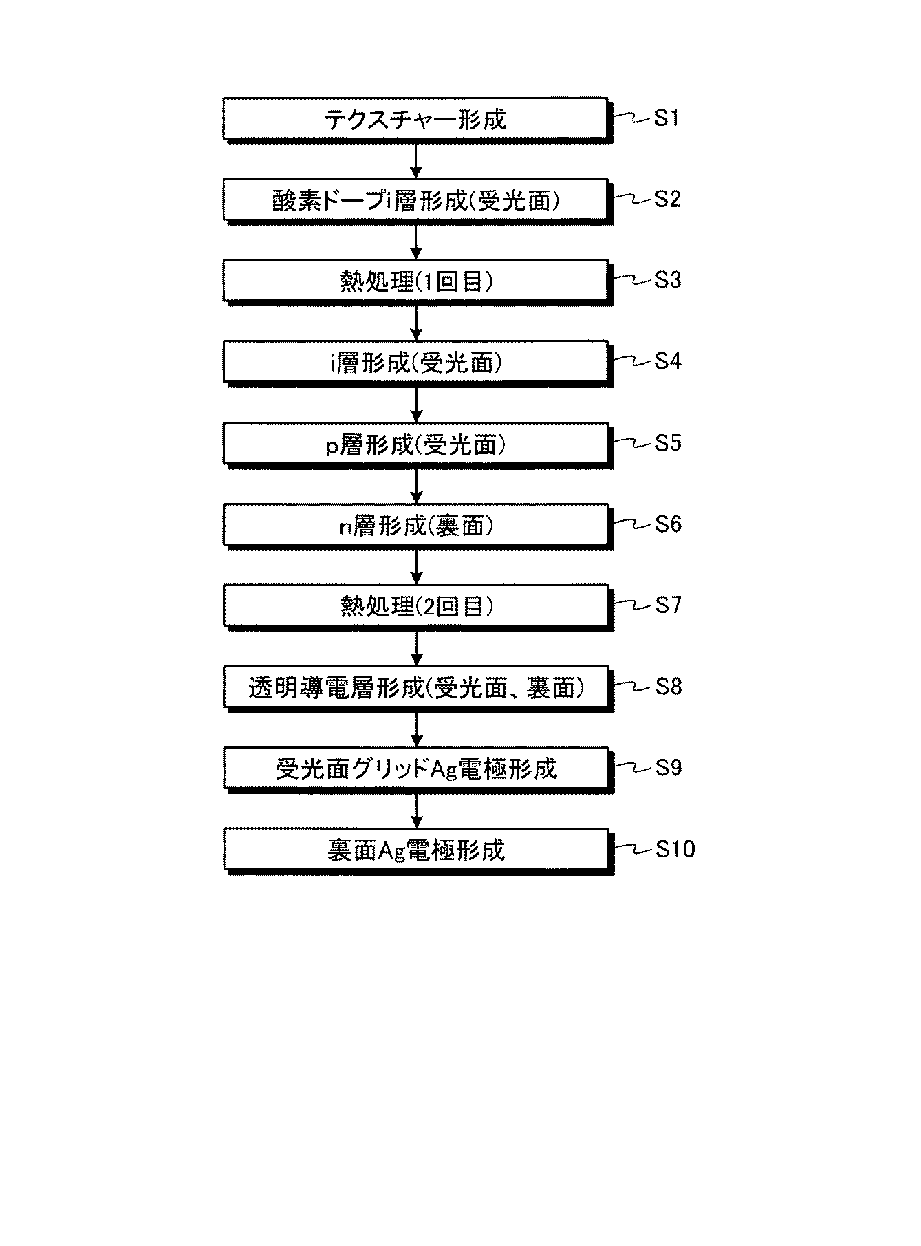
図2は、図1の太陽電池セル(太陽電池)30の製造プロセスの手順を示すフローチャートの図である。図2に沿って太陽電池セル30の製造プロセスを説明する。まず、1Ωcmのn型単結晶シリコンを材料とするn型単結晶シリコン基板1を、アルカリ溶液中に浸漬してスライス時のワイヤーソーダメージを除去すると同時に異方性エッチングによりテクスチャーを形成した(ステップS1)。
FIG. 2 is a flowchart showing the procedure of the manufacturing process of the solar battery cell (solar battery) 30 in FIG. The manufacturing process of the
その後、n型単結晶シリコン基板1をRCA洗浄によりクリーニングするとともに、希フッ酸で自然酸化膜除去を施し、27.56MHzのRFプラズマCVDチャンバで約1〜5nmの酸素ドープi型非晶質シリコン層2を形成した。酸素ドープi型非晶質シリコン層2は、RF出力50mW/cm2、基板温度200℃(第一の形成温度)、ガス圧500Paの雰囲気下で、シラン50sccm、水素500sccm、炭酸ガス5sccmを流して成膜することにより形成した(ステップS2)。 Thereafter, the n-type single crystal silicon substrate 1 is cleaned by RCA cleaning, a natural oxide film is removed with dilute hydrofluoric acid, and about 1 to 5 nm of oxygen-doped i-type amorphous silicon in a 27.56 MHz RF plasma CVD chamber. Layer 2 was formed. The oxygen-doped i-type amorphous silicon layer 2 is made to flow 50 sccm of silane, 500 sccm of hydrogen, and 5 sccm of carbon dioxide gas in an atmosphere of an RF output of 50 mW / cm 2 , a substrate temperature of 200 ° C. (first forming temperature), and a gas pressure of 500 Pa. (Step S2).
その後、フォーミングガス(水素5%含有の不活性ガス雰囲気)中で熱処理(1回目)を行った。本実施の形態では、熱処理温度による太陽電池特性への影響を調べるため、200、300、400、500℃の4種の温度(第一の熱処理温度)で各10分間の熱処理を実施した(ステップS3)。 Thereafter, heat treatment (first time) was performed in a forming gas (inert gas atmosphere containing 5% hydrogen). In this embodiment, in order to investigate the influence of the heat treatment temperature on the solar cell characteristics, heat treatment was performed for 10 minutes each at four temperatures (first heat treatment temperature) of 200, 300, 400, and 500 ° C. (step S3).
1回目の熱処理の後、プラズマCVDチャンバで1〜10nmの厚さのi型非晶質シリコン層3を形成した。i型非晶質シリコン層3は、RF出力50mW/cm2、基板温度190℃(第二の形成温度)、ガス圧500Paの雰囲気下で、シラン30sccm、水素500sccmを流して成膜することにより形成した(ステップS4)。
After the first heat treatment, an i-type amorphous silicon layer 3 having a thickness of 1 to 10 nm was formed in a plasma CVD chamber. The i-type amorphous silicon layer 3 is formed by flowing
続けて、プラズマCVDチャンバで約20nmの厚さのp型非晶質シリコン層4を形成した。成膜条件は基板温度140℃(第二の形成温度)、ガス圧500Paの雰囲気下で、100mW/cm2、シラン10sccm、水素100sccm、0.1%に水素希釈したジボラン20sccmとした(ステップS5)。 Subsequently, a p-type amorphous silicon layer 4 having a thickness of about 20 nm was formed in a plasma CVD chamber. The film forming conditions were a substrate temperature of 140 ° C. (second forming temperature) and a gas pressure of 500 Pa, 100 mW / cm 2 , silane 10 sccm, hydrogen 100 sccm, diborane 20 sccm diluted with 0.1% (Step S5). ).
次に、n型単結晶シリコン基板1の反対側の面に、CVDチャンバで約20nmのn型非晶質シリコン層5を製膜し、基板の裏面側にBSF構造を形成した。成膜条件は基板温度140℃(第二の形成温度)、ガス圧500Paの雰囲気下で、100mW/cm2、シラン10sccm、水素50sccm、1%に水素希釈したホスフィン50sccmとした(ステップS6)。 Next, an n-type amorphous silicon layer 5 having a thickness of about 20 nm was formed on the opposite side of the n-type single crystal silicon substrate 1 in a CVD chamber, and a BSF structure was formed on the back side of the substrate. The film forming conditions were 100 mW / cm 2 , silane 10 sccm, hydrogen 50 sccm, hydrogen phosphine 50 sccm diluted to 1% with hydrogen at a substrate temperature of 140 ° C. (second forming temperature) and a gas pressure of 500 Pa (step S 6).
その後、フォーミングガス(水素5%含有の不活性ガス雰囲気)中で200℃(第二の熱処理温度)で10分間の熱処理(2回目)を行った(ステップS7)。 Thereafter, a heat treatment (second time) was performed for 10 minutes at 200 ° C. (second heat treatment temperature) in a forming gas (inert gas atmosphere containing 5% hydrogen) (step S7).
そして、p型非晶質シリコン層4の表面に、表面電極としてに約70〜90nmの厚みを有する透明導電層(ITO)6を形成し(ステップS8)、その上に集電極として受光面グリッドAg電極7をスクリーン印刷法で形成した(ステップS9)。 A transparent conductive layer (ITO) 6 having a thickness of about 70 to 90 nm is formed as a surface electrode on the surface of the p-type amorphous silicon layer 4 (step S8), and a light receiving surface grid is formed thereon as a collecting electrode. The Ag electrode 7 was formed by screen printing (Step S9).
また、裏面電極として、n型非晶質シリコン膜上に約70〜90nmの厚みを有する透明導電層(ITO)6を形成し(ステップS8)、その上にスパッタリング法で約100nmの厚みの裏面Ag電極8を全面に形成した(ステップS10)。 Further, a transparent conductive layer (ITO) 6 having a thickness of about 70 to 90 nm is formed on the n-type amorphous silicon film as a back electrode (step S8), and a back surface having a thickness of about 100 nm is formed thereon by sputtering. An Ag electrode 8 was formed on the entire surface (step S10).
上記製造方法で作製した太陽電池セル30を、AM1.5のスペクトルの100mW/cm2の光照射にて電流−電圧特性を評価した。その結果、酸素ドープi型非晶質シリコン層2形成後の熱処理(1回目)を300℃(第一の熱処理温度)で実施した太陽電池セルが最も特性が良かった。
The
比較のため、上記プロセスにて作製した太陽電池セル30と同じ結晶、同じ特性をもつ基板を用いて、酸素ドープi型非晶質シリコン層2形成後の熱処理(1回目)の有無、p型非晶質シリコン層4及びn型非晶質シリコン層5の形成後の熱処理(2回目)の有無で、表1のように比較例1,2として検討し、それ以外はすべて同じプロセスで太陽電池を作製した。そしてAM1.5のスペクトルで100mW/cm2の光照射にて電流−電圧特性を評価した。
For comparison, the presence or absence of heat treatment (first time) after forming the oxygen-doped i-type amorphous silicon layer 2 using a substrate having the same crystal and the same characteristics as the
酸素ドープi型非晶質シリコン層2形成後に300℃(第一の熱処理温度)で10分の熱処理をしたのち、p型、n型非晶質シリコン膜形成後に200℃(第二の熱処理温度)で10分間の熱処理をした太陽電池セル30が最も出力が高かった。表1のサンプルにおいて、標準プロセスである比較例1のサンプルより6mV高い開放電圧を得ることができた。その理由は、酸素ドープi型非晶質シリコン層2の製膜後に、高温側熱処理を行うことで、n型単結晶シリコン基板1と酸素ドープi型非晶質シリコン層2との界面に存在する欠陥密度を、効果的に低減できたためと考えられる。また、酸素ドープi型非晶質シリコン層2の形成後に熱処理を行わず、p型、n型非晶質シリコン層4、5形成後に高温側熱処理を実施した比較例2では、標準プロセスである比較例1のサンプルと比べて10mV低い開放電圧となった。i型非晶質シリコン層3、p型、n型非晶質シリコン層4、5の耐熱温度を超える高い温度で熱処理を行ったため、水素脱離等の膜質低下に伴い界面欠陥密度が増大し、太陽電池の出力も低下したと考えられる。
After the oxygen-doped i-type amorphous silicon layer 2 is formed, heat treatment is performed at 300 ° C. (first heat treatment temperature) for 10 minutes, and after the formation of the p-type and n-type amorphous silicon films, 200 ° C. (second heat treatment temperature). The
上記のように、本実施の形態においては、n型単結晶シリコン基板1上に酸素ドープi型非晶質シリコン層2と、i型非晶質シリコン層3とが順に形成される構造において、酸素ドープi型非晶質シリコン層2を形成した後、i型非晶質シリコン層3や、p型、n型非晶質シリコン層4、5形成の耐熱温度よりも高い温度で熱処理を施すことにより、結晶シリコン基板と酸素ドープi型非晶質シリコン層2との界面特性の改善が可能となり、太陽電池の出力が向上した。 As described above, in the present embodiment, in the structure in which the oxygen-doped i-type amorphous silicon layer 2 and the i-type amorphous silicon layer 3 are sequentially formed on the n-type single crystal silicon substrate 1, After the oxygen-doped i-type amorphous silicon layer 2 is formed, heat treatment is performed at a temperature higher than the heat resistance temperature for forming the i-type amorphous silicon layer 3 and the p-type and n-type amorphous silicon layers 4 and 5. As a result, the interface characteristics between the crystalline silicon substrate and the oxygen-doped i-type amorphous silicon layer 2 can be improved, and the output of the solar cell is improved.
なお、i型非晶質シリコン層3や、その後形成されるp型非晶質シリコン層4、反対側の面のn型非晶質シリコン層5の形成温度(第二の形成温度)は、酸素ドープi型非晶質シリコン層2の形成温度(第一の形成温度)以下とすることが望ましい。酸素ドープi型非晶質シリコン層2に比べて、それより後に形成される膜(層)は耐熱性の点で劣り、酸素ドープi型非晶質シリコン層2の形成温度よりも高い温度で形成すると、特性が低下する傾向が見られるからである。 The formation temperature (second formation temperature) of the i-type amorphous silicon layer 3, the p-type amorphous silicon layer 4 formed thereafter, and the n-type amorphous silicon layer 5 on the opposite surface is: It is desirable that the temperature be lower than the formation temperature (first formation temperature) of the oxygen-doped i-type amorphous silicon layer 2. Compared to the oxygen-doped i-type amorphous silicon layer 2, the film (layer) formed after that is inferior in heat resistance and at a temperature higher than the formation temperature of the oxygen-doped i-type amorphous silicon layer 2. This is because, when formed, the characteristics tend to deteriorate.
なお、本実施の形態では、基材となる基板として、単結晶基板であるn型単結晶シリコン基板1を用いているが、多結晶基板を用いてもよい。また、n型単結晶シリコン基板1の熱処理においては、フォーミングガス(水素5%含有の不活性ガス)を用いたが、酸素、窒素、アルゴン等を含んだ雰囲気ガスを用いてもよい。ただし、水素を含んだガスは、n型単結晶シリコン基板1と酸素ドープi型非晶質シリコン層2との界面を水素終端することによりパッシベーション効果を高め、また、非晶質膜中の欠陥も水素により修復されるため、水素を含んだガスを用いるのが望ましい。 In the present embodiment, n-type single crystal silicon substrate 1 which is a single crystal substrate is used as a substrate serving as a base material, but a polycrystalline substrate may be used. In the heat treatment of the n-type single crystal silicon substrate 1, a forming gas (inert gas containing 5% hydrogen) is used, but an atmospheric gas containing oxygen, nitrogen, argon, or the like may be used. However, the gas containing hydrogen enhances the passivation effect by hydrogen-termination of the interface between the n-type single crystal silicon substrate 1 and the oxygen-doped i-type amorphous silicon layer 2, and defects in the amorphous film Since hydrogen is also repaired, it is desirable to use a gas containing hydrogen.
また、本実施の形態においては、上記第一真性半導体層(酸素ドープi型非晶質シリコン層2)を熱処理(1回目)するときの熱処理温度(第一の熱処理温度)は、酸素ドープi型非晶質シリコン層2の形成温度(第一の形成温度)より5〜200℃高く、より好ましくは10〜150℃高くすることがよい。絶対温度では400℃以下にするのが好ましい。400℃より高くなると、酸素を含有する第一真性半導体層であっても水素脱離による膜質の劣化が顕著になり太陽電池セルの出力が低下するためである。熱処理時間は、熱処理(1回目)の温度に依存するが、1〜120分間程度で、5〜60分間がより好ましい。おおよそ熱処理(1回目)の温度と熱処理時間とは反比例の関係になる。 In the present embodiment, the heat treatment temperature (first heat treatment temperature) when the first intrinsic semiconductor layer (oxygen-doped i-type amorphous silicon layer 2) is heat-treated (first time) is oxygen-doped i. The temperature is preferably 5 to 200 ° C., more preferably 10 to 150 ° C. higher than the formation temperature (first formation temperature) of the type amorphous silicon layer 2. The absolute temperature is preferably 400 ° C. or lower. This is because when the temperature is higher than 400 ° C., even in the first intrinsic semiconductor layer containing oxygen, the deterioration of the film quality due to hydrogen desorption becomes remarkable, and the output of the solar battery cell is lowered. The heat treatment time depends on the temperature of the heat treatment (first time), but is about 1 to 120 minutes, and more preferably 5 to 60 minutes. The temperature of the heat treatment (first time) is approximately inversely proportional to the heat treatment time.
また、本実施の形態では、受光面側のi型非晶質シリコン層3について検討したが、裏面側のn型単結晶シリコン基板1とn型非晶質シリコン層5との界面にi型非晶質シリコン層を挿入する場合には、このi型非晶質シリコン層についても、同様の処理を行って同様の効果が得られる。 In the present embodiment, the i-type amorphous silicon layer 3 on the light-receiving surface side has been studied, but i-type is formed at the interface between the n-type single crystal silicon substrate 1 and the n-type amorphous silicon layer 5 on the back surface side. When an amorphous silicon layer is inserted, the same effect can be obtained by performing the same process on the i-type amorphous silicon layer.
また、本実施の形態では、2回目の熱処理を、p型非晶質シリコン層4及びn型非晶質シリコン層5の形成後に実施したが、透明導電層(ITO)6の生成後以降で実施しても同様の効果が期待することができる。 In the present embodiment, the second heat treatment is performed after the formation of the p-type amorphous silicon layer 4 and the n-type amorphous silicon layer 5, but after the formation of the transparent conductive layer (ITO) 6. Even if implemented, the same effect can be expected.
以上のように、本発明にかかる光起電力装置及びその製造方法は、太陽電池などの光起電力装置及びその製造方法に適用されて有用なものであり、特に、結晶シリコン系太陽電池において高効率化が可能なヘテロ接合太陽電池及びその製造方法に適用されて最適なものである。 As described above, the photovoltaic device and the manufacturing method thereof according to the present invention are useful when applied to a photovoltaic device such as a solar cell and the manufacturing method thereof. It is optimally applied to a heterojunction solar cell capable of increasing efficiency and a method for manufacturing the same.
1 n型単結晶シリコン基板(第一導電型結晶系半導体基板)
2 酸素ドープi型非晶質シリコン層(第一の酸素濃度の第一真性半導体層)
3 i型非晶質シリコン層(第二の酸素濃度の第二真性半導体層)
4 p型非晶質シリコン層(第二導電型の非晶質半導体層)
5 n型非晶質シリコン層(第一導電型の非晶質半導体層)
6 透明導電層(ITO)
7 受光面グリッドAg電極
8 裏面Ag電極
30 太陽電池セル(太陽電池)
1 n-type single crystal silicon substrate (first conductivity type crystalline semiconductor substrate)
2 Oxygen-doped i-type amorphous silicon layer (first intrinsic semiconductor layer having a first oxygen concentration)
3 i-type amorphous silicon layer (second intrinsic semiconductor layer having a second oxygen concentration)
4 p-type amorphous silicon layer (second conductivity type amorphous semiconductor layer)
5 n-type amorphous silicon layer (first conductivity type amorphous semiconductor layer)
6 Transparent conductive layer (ITO)
7 Photosensitive surface grid Ag electrode 8 Back
Claims (10)
前記真性な非晶質半導体層は、前記基板側から積層された第一の酸素濃度の第一真性半導体層と、前記第一の酸素濃度より低い第二の酸素濃度の第二真性半導体層とから構成される光起電力装置において、
前記第一真性半導体層は、第一の形成温度にて形成の後、前記第一の形成温度より高い第一の熱処理温度で熱処理され、前記第二真性半導体層、前記第二導電型非晶質半導体層、および前記第一導電型非晶質半導体層は、前記第一の形成温度以下の第二の形成温度で形成されていることを特徴とする光起電力装置。 Forming a first conductive type crystalline semiconductor substrate and an intrinsic amorphous semiconductor layer and a second conductive type amorphous semiconductor layer in this order from the substrate side on the first surface of the first conductive type crystalline semiconductor substrate Each layer formed, and a first conductivity type amorphous semiconductor layer formed on a second surface opposite to the first surface of the first conductivity type crystalline semiconductor substrate,
The intrinsic amorphous semiconductor layer includes a first intrinsic semiconductor layer having a first oxygen concentration stacked from the substrate side, and a second intrinsic semiconductor layer having a second oxygen concentration lower than the first oxygen concentration. In the photovoltaic device composed of
The first intrinsic semiconductor layer is formed at a first formation temperature and then heat treated at a first heat treatment temperature higher than the first formation temperature, and the second intrinsic semiconductor layer, the second conductivity type amorphous The photovoltaic device and the first conductive amorphous semiconductor layer are formed at a second formation temperature lower than the first formation temperature.
ことを特徴とする請求項1に記載の光起電力装置。 The photovoltaic device according to claim 1, wherein the heat treatment is performed in a forming gas atmosphere.
ことを特徴とする請求項1または2に記載の光起電力装置。 The photovoltaic device according to claim 1 or 2, wherein the first heat treatment temperature is higher by 5 to 200 ° C than the first formation temperature.
ことを特徴とする請求項1から4のいずれか1項に記載の光起電力装置。 5. The light according to claim 1, wherein the first intrinsic semiconductor layer has a thickness of 1 nm to 5 nm and the second intrinsic semiconductor layer has a thickness of 1 nm to 10 nm. Electromotive force device.
前記真性な非晶質半導体層は、前記基板側から積層された第一の酸素濃度の第一真性半導体層と、前記第一の酸素濃度より低い第二の酸素濃度の第二真性半導体層とから構成される光起電力装置の製造方法において、
第一の形成温度にて前記第一真性半導体層を形成の後、前記第一真性半導体層を前記第一の形成温度より高い第一の熱処理温度で熱処理すると共に、前記第一の形成温度以下の第二の形成温度で、前記第二真性半導体層、前記第二導電型非晶質半導体層、および前記第一導電型非晶質半導体層を形成することを特徴とする光起電力装置の製造方法。 Forming a first conductive type crystalline semiconductor substrate and an intrinsic amorphous semiconductor layer and a second conductive type amorphous semiconductor layer in this order from the substrate side on the first surface of the first conductive type crystalline semiconductor substrate Each layer formed, and a first conductivity type amorphous semiconductor layer formed on a second surface opposite to the first surface of the first conductivity type crystalline semiconductor substrate,
The intrinsic amorphous semiconductor layer includes a first intrinsic semiconductor layer having a first oxygen concentration stacked from the substrate side, and a second intrinsic semiconductor layer having a second oxygen concentration lower than the first oxygen concentration. In a method for producing a photovoltaic device comprising:
After forming the first intrinsic semiconductor layer at a first formation temperature, the first intrinsic semiconductor layer is heat-treated at a first heat treatment temperature higher than the first formation temperature, and less than the first formation temperature. And forming the second intrinsic semiconductor layer, the second conductive amorphous semiconductor layer, and the first conductive amorphous semiconductor layer at a second formation temperature of the photovoltaic device. Production method.
ことを特徴とする請求項6に記載の光起電力装置の製造方法。 The method for manufacturing a photovoltaic device according to claim 6, wherein the heat treatment is performed in a forming gas atmosphere.
ことを特徴とする請求項6または7に記載の光起電力装置の製造方法。 The method for manufacturing a photovoltaic device according to claim 6, wherein the first heat treatment temperature is higher by 5 to 200 ° C. than the first formation temperature.
ことを特徴とする請求項6から9のいずれか1項に記載の光起電力装置の製造方法。 The thickness of said 1st intrinsic semiconductor layer shall be 1 nm or more and 5 nm or less, and the thickness of said 2nd intrinsic semiconductor layer shall be 1 nm or more and 10 nm or less. Photovoltaic device manufacturing method.
Priority Applications (1)
| Application Number | Priority Date | Filing Date | Title |
|---|---|---|---|
| JP2011122665A JP2012253091A (en) | 2011-05-31 | 2011-05-31 | Photovoltaic device and method for manufacturing the same |
Applications Claiming Priority (1)
| Application Number | Priority Date | Filing Date | Title |
|---|---|---|---|
| JP2011122665A JP2012253091A (en) | 2011-05-31 | 2011-05-31 | Photovoltaic device and method for manufacturing the same |
Publications (1)
| Publication Number | Publication Date |
|---|---|
| JP2012253091A true JP2012253091A (en) | 2012-12-20 |
Family
ID=47525663
Family Applications (1)
| Application Number | Title | Priority Date | Filing Date |
|---|---|---|---|
| JP2011122665A Withdrawn JP2012253091A (en) | 2011-05-31 | 2011-05-31 | Photovoltaic device and method for manufacturing the same |
Country Status (1)
| Country | Link |
|---|---|
| JP (1) | JP2012253091A (en) |
Cited By (3)
| Publication number | Priority date | Publication date | Assignee | Title |
|---|---|---|---|---|
| CN103178148A (en) * | 2013-04-21 | 2013-06-26 | 常州合特光电有限公司 | Thin film/heterojunction lamination type solar battery and manufacturing method thereof |
| JP2014203924A (en) * | 2013-04-03 | 2014-10-27 | 三菱電機株式会社 | Process of manufacturing solar cell and solar cell |
| JP2017017323A (en) * | 2015-06-30 | 2017-01-19 | エルジー エレクトロニクス インコーポレイティド | Solar cell and method of manufacturing the same |
-
2011
- 2011-05-31 JP JP2011122665A patent/JP2012253091A/en not_active Withdrawn
Cited By (5)
| Publication number | Priority date | Publication date | Assignee | Title |
|---|---|---|---|---|
| JP2014203924A (en) * | 2013-04-03 | 2014-10-27 | 三菱電機株式会社 | Process of manufacturing solar cell and solar cell |
| CN103178148A (en) * | 2013-04-21 | 2013-06-26 | 常州合特光电有限公司 | Thin film/heterojunction lamination type solar battery and manufacturing method thereof |
| JP2017017323A (en) * | 2015-06-30 | 2017-01-19 | エルジー エレクトロニクス インコーポレイティド | Solar cell and method of manufacturing the same |
| US10566487B2 (en) | 2015-06-30 | 2020-02-18 | Lg Electronics Inc. | Solar cell and method of manufacturing the same |
| US11462654B2 (en) | 2015-06-30 | 2022-10-04 | Lg Electronics Inc. | Solar cell and method of manufacturing the same |
Similar Documents
| Publication | Publication Date | Title |
|---|---|---|
| JP5456168B2 (en) | Method for manufacturing photoelectric conversion device | |
| JP3926800B2 (en) | Manufacturing method of tandem type thin film photoelectric conversion device | |
| US6566159B2 (en) | Method of manufacturing tandem thin-film solar cell | |
| JP5058184B2 (en) | Method for manufacturing photovoltaic device | |
| JP5183588B2 (en) | Method for manufacturing photovoltaic device | |
| TWI496300B (en) | Solar cell with heterojunction and manufacturing method thereof | |
| JP2020017763A (en) | Manufacturing method of photoelectric conversion device | |
| JP5052309B2 (en) | Photovoltaic device and manufacturing method thereof | |
| JP2012227281A (en) | Crystalline silicon solar cell | |
| JP5307688B2 (en) | Crystalline silicon solar cell | |
| JP2014072406A (en) | Solar cell and manufacturing method therefor, solar cell module | |
| JP5232362B2 (en) | A manufacturing method of an integrated thin film photoelectric conversion device, and an integrated thin film photoelectric conversion device obtainable by the manufacturing method. | |
| JP2019033201A (en) | Crystalline silicon type solar cell | |
| JP4711851B2 (en) | Photovoltaic device | |
| JP5745653B2 (en) | Photovoltaic device, manufacturing method thereof, and photovoltaic module | |
| JP2012253091A (en) | Photovoltaic device and method for manufacturing the same | |
| KR20130035876A (en) | Photoelectric conversion device | |
| JP2014072416A (en) | Solar cell and manufacturing method therefor, solar cell module | |
| JP5268976B2 (en) | Method for manufacturing photovoltaic device | |
| JP5748907B2 (en) | Photovoltaic device and manufacturing method thereof | |
| JP2014011198A (en) | Photovoltaic device and method for manufacturing the same | |
| TWI790245B (en) | Manufacturing method of photoelectric conversion device | |
| JP5398772B2 (en) | Photovoltaic device, manufacturing method thereof, and photovoltaic module | |
| WO2010067704A1 (en) | Photovoltaic device and method for manufacturing same | |
| JP2005191024A (en) | Photovoltaic power device and its manufacturing method |
Legal Events
| Date | Code | Title | Description |
|---|---|---|---|
| A300 | Application deemed to be withdrawn because no request for examination was validly filed |
Free format text: JAPANESE INTERMEDIATE CODE: A300 Effective date: 20140805 |