JP2012234603A - Method for inspecting film thickness of transferred object, method for producing transferred object, apparatus for producing transferred object, and stamper for transfer - Google Patents
Method for inspecting film thickness of transferred object, method for producing transferred object, apparatus for producing transferred object, and stamper for transfer Download PDFInfo
- Publication number
- JP2012234603A JP2012234603A JP2011104259A JP2011104259A JP2012234603A JP 2012234603 A JP2012234603 A JP 2012234603A JP 2011104259 A JP2011104259 A JP 2011104259A JP 2011104259 A JP2011104259 A JP 2011104259A JP 2012234603 A JP2012234603 A JP 2012234603A
- Authority
- JP
- Japan
- Prior art keywords
- film thickness
- pattern
- resin agent
- transferred
- stamper
- Prior art date
- Legal status (The legal status is an assumption and is not a legal conclusion. Google has not performed a legal analysis and makes no representation as to the accuracy of the status listed.)
- Pending
Links
Images


Classifications
-
- G—PHYSICS
- G11—INFORMATION STORAGE
- G11B—INFORMATION STORAGE BASED ON RELATIVE MOVEMENT BETWEEN RECORD CARRIER AND TRANSDUCER
- G11B5/00—Recording by magnetisation or demagnetisation of a record carrier; Reproducing by magnetic means; Record carriers therefor
- G11B5/84—Processes or apparatus specially adapted for manufacturing record carriers
- G11B5/855—Coating only part of a support with a magnetic layer
Landscapes
- Length Measuring Devices By Optical Means (AREA)
- Shaping Of Tube Ends By Bending Or Straightening (AREA)
- Manufacturing Of Magnetic Record Carriers (AREA)
Abstract
【課題】安価な装置で簡便にレジスト膜の膜厚を測定できるようする。
【解決手段】被転写物膜厚検査方法は、所定のパターンの設けられたスタンパを被転写物用基板に塗布された光硬化樹脂剤に押圧すると共に光硬化樹脂剤にUV光線を照射し、硬化後にスタンパを剥離することによってスタンパの所定のパターンの転写された被転写物用基板を製造する際に、光硬化樹脂剤に転写されたパターンの所定箇所を観察することによって、光硬化樹脂剤の膜厚が適切であるか否かを検査する。所定のパターンが設けられていない部分に、それぞれ幅または深さの異なるパターンを膜厚測定用パターンとして設けたスタンパによって転写し、この膜厚測定用パターン内のどのパターンに光硬化樹脂が充填されているか否かを観察することによって、被転写物用基板に塗布された光硬化樹脂剤の膜厚を測定する。
【選択図】図2A film thickness of a resist film can be easily measured with an inexpensive apparatus.
A method for inspecting a film thickness of a transferred material is a method in which a stamper provided with a predetermined pattern is pressed against a photocurable resin agent applied to a substrate for an object to be transferred and irradiated with UV light. A photocurable resin agent is obtained by observing a predetermined portion of a pattern transferred to a photocurable resin agent when a substrate for a transferred object having a predetermined pattern transferred to the stamper is manufactured by peeling the stamper after curing. Inspect whether the film thickness is appropriate. A pattern with a different width or depth is transferred to a portion where a predetermined pattern is not provided by a stamper provided as a film thickness measurement pattern, and any pattern in the film thickness measurement pattern is filled with a photocurable resin. The film thickness of the photo-curing resin agent applied to the substrate for transfer object is measured by observing whether or not it is.
[Selection] Figure 2
Description
本発明は、高密度記録のディスクの膜厚を検査する被転写物膜厚検査方法、被転写物製造方法及び被転写物製造装置並びに転写用スタンパに係り、特に転写ディスクの膜厚を正確に測定することのできる被転写物膜厚検査方法、被転写物製造方法及び被転写物製造装置並びに転写用スタンパに関する。 The present invention relates to a transfer object film thickness inspection method, a transfer object manufacturing method, a transfer object manufacturing apparatus, and a transfer stamper for inspecting a film thickness of a high density recording disk. The present invention relates to a transfer film thickness inspection method, a transfer object manufacturing method, a transfer object manufacturing apparatus, and a transfer stamper that can be measured.
ハードディスクデバイス(HDD)の記録媒体であるディスクは、アルミニウムやガラスなどの円板をベースとし、その表面に磁性膜が塗布され、さらに、その上に保護膜がコーテングされて構成されている。この磁性膜の膜厚は、磁気ヘッドで情報を記録・再生するときの磁気的特性に影響を与えるので、ディスクの製造時にはその膜厚を検査して、その精度を管理することが重要である。この磁性膜の膜厚の検査を正確に検査するディスク媒体の膜厚測定方法として特許文献1に示すようなものが知られている。 A disk, which is a recording medium of a hard disk device (HDD), is based on a disk such as aluminum or glass, a magnetic film is applied on the surface, and a protective film is further coated thereon. Since the thickness of this magnetic film affects the magnetic characteristics when information is recorded / reproduced by a magnetic head, it is important to check the film thickness and manage its accuracy when manufacturing the disk. . As a method for measuring the thickness of a disk medium for accurately inspecting the thickness of the magnetic film, a method as disclosed in Patent Document 1 is known.
特許文献1に示すディスク媒体の膜厚測定方法は、波長の異なる2以上のレーザビームを別々に磁性膜に照射して、それぞれの反射光によって発生する干渉光の光強度の強い部分の値のうち、最も近い値を求めることで、正しい膜厚を測定している。従来の膜厚検査方法は、測定のために2以上のレーザビームを必要としており、装置全体が高価であった。 The method of measuring the film thickness of the disk medium disclosed in Patent Document 1 irradiates the magnetic film with two or more laser beams having different wavelengths separately, and the value of the portion where the light intensity of the interference light generated by each reflected light is strong. The correct film thickness is measured by obtaining the closest value. The conventional film thickness inspection method requires two or more laser beams for measurement, and the entire apparatus is expensive.
この発明は、上述の点に鑑みなされたものであって、安価な装置で簡便にレジスト膜などの被転写物の膜厚を測定することのできる被転写物膜厚検査方法、被転写物製造方法及び被転写物製造装置並びに転写用スタンパを提供することを目的とする。 The present invention has been made in view of the above-described points, and can provide a method for inspecting a film thickness of a transferred material, which can easily measure the film thickness of the transferred material such as a resist film, and the manufacture of the transferred material. It is an object of the present invention to provide a method, a transfer object manufacturing apparatus, and a transfer stamper.
本発明に係る被転写物膜厚検査方法の第1の特徴は、所定のパターンの設けられたスタンパを被転写物用基板に塗布された光硬化樹脂剤に押圧すると共に前記光硬化樹脂剤にUV光線を照射し、硬化後に前記スタンパを剥離することによって前記スタンパの所定のパターンの転写された被転写物用基板を製造する際に、前記光硬化樹脂剤に転写された前記パターンの所定箇所を観察することによって、前記光硬化樹脂剤の膜厚が適切であるか否かを検査することにある。ナノインプリント装置などのようにスタンパによって所定のパターンの転写される被転写物用基板の表面には、サーボパターンのバースト領域などのように非記録部分を有するので、この部分を光学顕微鏡やカメラなどで観察して、レジスト充填率を多く要する。非記録部分に光硬化樹脂剤(レジスト剤)が十分に充填されていなければ、被転写物用基板全体に十分な量の光硬化樹脂剤が塗布されずに、膜厚が薄くなっている箇所が存在すると判断することができ、逆の場合は被転写物用基板全体に十分な量の光硬化樹脂剤が塗布されたと判断することができる。ここで、非記録部分とは、ディスクの読み書きをする上で、ディスク上に何らかの情報が書き込まれる部分以外の部分をいう。 A first feature of the film thickness inspection method for a transferred object according to the present invention is that a stamper provided with a predetermined pattern is pressed against a photocurable resin agent applied to a substrate for the transferred object, and the photocurable resin agent is When manufacturing a substrate for a transferred object to which a predetermined pattern of the stamper is transferred by irradiating UV light and peeling off the stamper after curing, a predetermined portion of the pattern transferred to the photocurable resin agent Is to check whether the film thickness of the photocurable resin agent is appropriate. Since the surface of the substrate for the object to which a predetermined pattern is transferred by a stamper such as a nanoimprint apparatus has a non-recorded part such as a burst area of a servo pattern, this part can be removed with an optical microscope or a camera. Observe a large resist filling rate. If the non-recording part is not sufficiently filled with a photo-curing resin agent (resist agent), a portion where the film thickness is reduced without applying a sufficient amount of the photo-curing resin agent to the entire substrate for the object to be transferred In the opposite case, it can be determined that a sufficient amount of the photo-curing resin agent has been applied to the entire substrate for transferred object. Here, the non-recording portion refers to a portion other than a portion where some information is written on the disc when reading / writing the disc.
本発明に係る被転写物膜厚検査方法の第2の特徴は、前記第1の特徴に記載の被転写物膜厚検査方法において、前記光硬化樹脂剤に転写された前記パターンの所定箇所として、前記被転写物用基板の非記録領域を観察し、前記領域に前記光硬化樹脂が充填されていない部分があればその箇所の膜厚は薄いと判定することにある。これは、光硬化樹脂剤の膜厚が適切であるか否かを検査するのに、レジスト充填率の多い非記録領域を観察するようにしたものである。 A second feature of the transferred object film thickness inspection method according to the present invention is the transferred material film thickness inspection method according to the first feature, wherein the pattern transferred to the photo-curing resin agent is a predetermined portion. The non-recording area of the substrate for transfer object is observed, and if there is a part that is not filled with the photocurable resin in the area, it is determined that the film thickness of that part is thin. In this case, in order to inspect whether or not the film thickness of the photo-curing resin agent is appropriate, a non-recording area with a high resist filling rate is observed.
本発明に係る被転写物膜厚検査方法の第3の特徴は、所定のパターンの設けられたスタンパを被転写物用基板に塗布された光硬化樹脂剤に押圧すると共に前記光硬化樹脂剤にUV光線を照射し、硬化後に前記スタンパを剥離することによって前記スタンパの所定のパターンの転写された被転写物用基板を製造する際に、前記スタンパに前記所定のパターンとは別個の膜厚測定用のパターンを設け、前記光硬化樹脂剤に転写された前記膜厚測定用パターンを観察し、前記膜厚測定用パターン内に前記光硬化樹脂が充填されているか否かによって、前記光硬化樹脂剤の膜厚を測定することにある。これは、スタンパにおいて所定のパターンが設けられていない部分に、それぞれ幅の異なるパターンを膜厚測定用パターンとして設け、このスタンパによって転写された被転写物用基板の膜厚測定用パターン内のどのパターンに光硬化樹脂が充填されているか否かを観察することによって、被転写物用基板に塗布された光硬化樹脂剤の膜厚を測定するようにしたものである。この膜厚測定用パターンは、被転写物用基板に転写した際に、例えば膜厚が20nmの時に光硬化樹脂剤(レジスト剤)が充填されるパターン、膜厚が40nmの時にレジスト剤が充填されるパターン、膜厚が60mmの時にレジスト剤が充填されるパターンのように、膜厚に対応して充填される幅をそれぞれ有するものである。これによって、専用の測定機器を用いなくてもレジスト剤の充填の様子を観察することで容易に膜厚を測定することができる。 A third feature of the transferred object film thickness inspection method according to the present invention is that the stamper provided with a predetermined pattern is pressed against the photocurable resin agent applied to the substrate for the transferred object, and the photocurable resin agent is applied to the photocurable resin agent. When manufacturing a substrate for a transferred object on which a predetermined pattern of the stamper is transferred by irradiating with UV light and peeling off the stamper after curing, film thickness measurement different from the predetermined pattern on the stamper The film thickness measurement pattern transferred to the photocurable resin agent is observed, and the photocurable resin is determined depending on whether the photocurable resin is filled in the film thickness measurement pattern. The purpose is to measure the film thickness of the agent. This is because a pattern having a different width is provided as a film thickness measurement pattern in a portion where a predetermined pattern is not provided in the stamper, and any of the film thickness measurement patterns of the substrate for transferred material transferred by the stamper is selected. By observing whether or not the pattern is filled with a photo-curing resin, the film thickness of the photo-curing resin agent applied to the substrate for transfer object is measured. This film thickness measurement pattern is, for example, a pattern that is filled with a photo-curing resin agent (resist agent) when the film thickness is 20 nm when transferred to the substrate for a transfer object, and a resist agent that is filled when the film thickness is 40 nm. Each pattern has a width filled corresponding to the film thickness, such as a pattern filled with a resist agent when the film thickness is 60 mm. Accordingly, the film thickness can be easily measured by observing the state of filling the resist agent without using a dedicated measuring instrument.
本発明に係る被転写物製造方法の第1の特徴は、被転写物用基板に光硬化樹脂剤を塗布するステップと、前記光硬化樹脂剤に所定のパターンの設けられたスタンパを押圧するステップと、前記光硬化樹脂剤にUV光線を照射するステップと、前記UV光線の照射によって硬化した前記光硬化樹脂から前記スタンパを剥離するステップと、前記スタンパ剥離後に前記光硬化樹脂剤に転写された前記パターンの所定箇所を観察し、前記光硬化樹脂剤の膜厚が適切であるか否かを判断するステップとを含むことにある。これは、前記被転写物膜厚検査方法の第1の特徴に対応した被転写物製造方法の発明である。 The first feature of the transfer object manufacturing method according to the present invention is a step of applying a photocurable resin agent to the transfer object substrate, and a step of pressing a stamper provided with a predetermined pattern on the photocurable resin agent. And a step of irradiating the photo-curing resin agent with UV light, a step of peeling the stamper from the photo-curing resin cured by irradiation of the UV light, and a transfer to the photo-curing resin agent after the stamper peeling. Observing a predetermined portion of the pattern and determining whether or not the film thickness of the photocurable resin agent is appropriate. This is an invention of a transferred object manufacturing method corresponding to the first feature of the transferred object film thickness inspection method.
本発明に係る被転写物製造方法の第2の特徴は、前記第4の特徴に記載の被転写物製造方法において、前記光硬化樹脂剤に転写された前記パターンの所定箇所として、非記録領域を観察し、前記非記録領域に前記光硬化樹脂が充填されていない部分があればその箇所の膜厚は薄いと判定することにある。これは、前記被転写物膜厚検査方法の第2の特徴に対応した被転写物製造方法の発明である。 A second feature of the transferred object manufacturing method according to the present invention is the transferred object manufacturing method according to the fourth feature, wherein a non-recording area is used as the predetermined portion of the pattern transferred to the photocurable resin agent. If there is a portion where the photo-curing resin is not filled in the non-recording area, it is determined that the film thickness of the portion is thin. This is an invention of a transfer object manufacturing method corresponding to the second feature of the transfer object film thickness inspection method.
本発明に係る被転写物製造方法の第3の特徴は、被転写物用基板に光硬化樹脂剤を塗布するステップと、前記光硬化樹脂剤に前記被転写物用基板固有のパターン及び膜厚測定用パターンの設けられたスタンパを押圧するステップと、前記光硬化樹脂剤にUV光線を照射するステップと、前記UV光線の照射によって硬化した前記光硬化樹脂から前記スタンパを剥離するステップと、前記スタンパ剥離後に前記光硬化樹脂剤に転写された前記膜厚測定用パターンを観察し、前記膜厚測定用パターン内に前記光硬化樹脂が充填されているか否かによって、前記光硬化樹脂剤の膜厚を測定するステップとを含むことにある。これは、前記被転写物膜厚検査方法の第3の特徴に対応した被転写物製造方法の発明である。 The third feature of the transferred object manufacturing method according to the present invention is that a photocurable resin agent is applied to the transferred object substrate, and the pattern and film thickness unique to the transferred object substrate on the photocurable resin agent. Pressing a stamper provided with a measurement pattern, irradiating the photocurable resin agent with UV light, peeling the stamper from the photocured resin cured by irradiation with the UV light, The film thickness measurement pattern transferred to the photocurable resin agent after the stamper peeling is observed, and the photocurable resin agent film is determined depending on whether the photocurable resin is filled in the film thickness measurement pattern. Measuring the thickness. This is an invention of a transfer object manufacturing method corresponding to the third feature of the transfer object film thickness inspection method.
本発明に係る被転写物製造装置の第1の特徴は、被転写物用基板に光硬化樹脂剤を塗布する樹脂剤塗布手段と、前記樹脂剤塗布手段によって前記被転写物用基板に塗布された前記光硬化樹脂剤に所定のパターンの設けられたスタンパを押圧すると共に前記光硬化樹脂剤にUV光線を照射して前記光硬化樹脂剤を硬化させるパターン転写手段と、硬化した前記光硬化樹脂剤から前記スタンパを剥離する剥離手段と、前記スタンパ剥離後に前記光硬化樹脂剤に転写された前記パターンの所定箇所を観察し、前記光硬化樹脂剤の膜厚が適切であるか否かを判断する膜厚判断手段とを備えたことにある。これは、前記被転写物製造方法の第1の特徴に対応した被転写物製造装置の発明である。 The first feature of the transfer object manufacturing apparatus according to the present invention is that the transfer agent substrate is applied to the transfer object substrate by the resin agent applying means for applying a photocurable resin agent to the transfer object substrate, and the resin agent applying means. A pattern transfer means for pressing the stamper provided with a predetermined pattern on the photocurable resin agent and irradiating the photocurable resin agent with UV light to cure the photocurable resin agent; and the cured photocurable resin. A peeling means for peeling the stamper from the agent, and a predetermined portion of the pattern transferred to the photocurable resin agent after the stamper is peeled off to determine whether the film thickness of the photocurable resin agent is appropriate And a film thickness judging means. This is an invention of a transfer object manufacturing apparatus corresponding to the first feature of the transfer object manufacturing method.
本発明に係る被転写物製造装置の第2の特徴は、前記第1の特徴に記載の被転写物製造装置において、前記膜厚判断手段は、前記光硬化樹脂剤に転写された前記パターンの所定箇所として、非記録領域を観察し、前記非記録領域に前記光硬化樹脂剤が充填されていない部分があればその箇所の膜厚は薄いと判定することにある。これは、前記被転写物製造方法の第2の特徴に対応した被転写物製造装置の発明である。 A second feature of the transferred object manufacturing apparatus according to the present invention is the transferred object manufacturing apparatus according to the first feature, wherein the film thickness determining means is configured to transfer the pattern transferred to the photocurable resin agent. As the predetermined portion, a non-recording area is observed, and if there is a portion not filled with the photocurable resin agent in the non-recording area, it is determined that the film thickness of the portion is thin. This is an invention of a transfer object manufacturing apparatus corresponding to the second feature of the transfer object manufacturing method.
本発明に係る被転写物製造装置の第3の特徴は、被転写物用基板に光硬化樹脂剤を塗布する樹脂剤塗布手段と、前記樹脂剤塗布手段によって前記被転写物用基板に塗布された前記光硬化樹脂剤に前記被転写物用基板固有のパターン及び膜厚測定用パターンの設けられたスタンパを押圧すると共に前記光硬化樹脂剤にUV光線を照射して前記光硬化樹脂剤を硬化させるパターン転写手段と、硬化した前記光硬化樹脂剤から前記スタンパを剥離する剥離手段と、前記スタンパ剥離後に前記光硬化樹脂剤に転写された前記膜厚測定用パターンを観察し、前記膜厚測定用パターン内に前記光硬化樹脂が充填されているか否かによって、前記光硬化樹脂剤の膜厚を測定する膜厚測定手段とを備えたことにある。これは、前記被転写物製造方法の第3の特徴に対応した被転写物製造装置の発明である。 A third feature of the transfer object manufacturing apparatus according to the present invention is that the transfer agent substrate is applied to the transfer object substrate by a resin agent applying unit that applies a photocurable resin agent to the transfer object substrate, and the resin agent applying unit. Further, the photocuring resin agent is pressed with a stamper provided with a pattern specific to the substrate to be transferred and a film thickness measurement pattern, and the photocuring resin agent is irradiated with UV light to cure the photocuring resin agent. Pattern transfer means, peeling means for peeling the stamper from the cured photocurable resin agent, and observation of the film thickness measurement pattern transferred to the photocurable resin agent after the stamper peeling, and measuring the film thickness A film thickness measuring means for measuring the film thickness of the photo-curing resin agent depending on whether or not the photo-curing resin is filled in the pattern for use. This is an invention of a transfer object manufacturing apparatus corresponding to the third feature of the transfer object manufacturing method.
本発明に係る転写用スタンパの特徴は、被転写物用基板固有のパターン及び膜厚測定用パターンを有し、光硬化樹脂剤の塗布された被転写物用基板に押圧されることによって前記被転写物用基板固有のパターン及び膜厚測定用パターンを前記光硬化樹脂剤に転写するように構成されたことにある。これは、前記ディスク検査方法の第3の特徴、前記被転写物製造方法の第3の特徴及び前記被転写物製造装置の第3の特徴で使用される転写用スタンパの発明である。 The transfer stamper according to the present invention is characterized by having a pattern unique to a substrate for a transfer object and a pattern for measuring a film thickness, and is pressed against the transfer object substrate coated with a photocurable resin agent. A pattern unique to a substrate for transfer and a pattern for measuring a film thickness are transferred to the photo-curing resin agent. This is an invention of a transfer stamper used in the third feature of the disk inspection method, the third feature of the transfer object manufacturing method, and the third feature of the transfer object manufacturing apparatus.
本発明によれば、安価な装置で簡便に被転写物の膜厚を測定することができるという効果がある。 According to the present invention, there is an effect that the film thickness of a transfer object can be easily measured with an inexpensive apparatus.
以下、図面に基いて説明する。図1は本発明のディスク膜厚測定方法を採用したディスクを作成するナノインプリント装置の概要構成を示す図である。このナノインプリント装置は、ローダ12、ディスク置き台13、ディスクマテハン14、スピンコータ15、転写ステージ16、UV光源17a,17b、転写プレス18、剥離ステージ19、アンローダ21から構成される。
Hereinafter, description will be made based on the drawings. FIG. 1 is a diagram showing a schematic configuration of a nanoimprint apparatus for producing a disc adopting the disc film thickness measuring method of the present invention. The nanoimprint apparatus includes a
ローダ12は被検査対象物となる被転写物用基板7aをディスク置き台13上に載置する。ディスク置き台13に載置された被転写物用基板7aは、ディスクマテハン14によってスピンコータ15上に設置される。スピンコータ15は光硬化樹脂を被転写物用基板7bの表面に塗布する。光硬化樹脂を表面に塗布された被転写物用基板7bは、ディスクマテハン14によって転写ステージ16上に設置されたスタンパ9aの上に載置される。なお、スタンパ9a上に載置されている被転写物用基板については図示を省略してある。被転写物用基板としては、ディスク基板やウエハー基板などである。
The
転写ステージ16と剥離ステージ19は、レール上を図の左右方向にスライド移動可能に構成されている。従って、光硬化樹脂が塗布された被転写物用基板7bがスタンパ9aの上に載置されると、転写ステージ16は、転写プレス18の下へと移動する。このとき剥離ステージ19は、アンローダ21の下に移動している。転写プレス18は、図示のようにその下側であって、スタンパ9aの上側にスタンパ9bを設置している。
The
転写プレス18が下降して、光硬化樹脂が塗布された被転写物用基板をスタンパ9aに押圧する。この押圧と同時に転写ステージ16に設置されているUV光源17a、及び転写プレス18に設置されているUV光源17bは、UV光線を被転写物用基板に照射し、被転写物用基板に塗布されている光硬化樹脂を硬化させる。これによってスタンパ9a,9bの各パターンが被転写物用基板の光硬化樹脂に転写される。
The
転写プレス18によるパターン転写後、転写プレス18が上昇することによって、被転写物用基板は転写ステージ16から剥離され、転写プレス18に付着した形となる。被転写物用基板の剥離された転写ステージ16は元の位置(ディスクマテハン14の下側)に移動する。一方、アンローダ21の下に位置していた剥離ステージ19は、転写プレス18の下へと移動する。転写プレス18は剥離ステージ19の位置まで下降する。剥離ステージ19は転写プレス18に付着している被転写物用基板を吸着する。その後、転写プレス18が上昇する。これによってスタンパ9bから被転写物用基板が剥離され、被転写物用基板は剥離ステージ19に付着される。剥離ステージ19はアンローダ21の下側へと移動し、被転写物用基板の吸着を解除する。その後、膜厚検査用のカメラや顕微鏡などの膜厚検査器20でレジスト膜厚を検査した後、アンローダ21が剥離ステージ19上から被転写物用基板を取り出す。
After the pattern is transferred by the
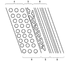
図2は本発明に係る被転写物膜厚検査方法の概要を示す図である。図3は図1のディスクのサーボパターンの概要を模式的に表した図である。図2に示すように、光硬化樹脂塗布前のディスク1には、法線方向に延びた複数本のサーボパターン3が形成されている。サーボパターン3は、図3に示すように、バースト4、グレーゾーン5、及びプレアンビル6から構成されている。これらは、ディスク1がハードディスクドライブ装置に組み込まれたときに、磁気ヘッドがデータの場所を探す際に必要な部位である。光硬化樹脂の未充填(充填量が規定量に達しない場合も含まれる)は、このレジスト充填量を多く必要とする非記録箇所で起こる。また、レジスト充填量を多く必要とする箇所はパターン原版の設計値による。
FIG. 2 is a diagram showing an outline of the transferred object film thickness inspection method according to the present invention. FIG. 3 is a diagram schematically showing an outline of the servo pattern of the disk of FIG. As shown in FIG. 2, a plurality of servo patterns 3 extending in the normal direction are formed on the disk 1 before application of the photocurable resin. As shown in FIG. 3, the servo pattern 3 is composed of a
そこで、この実施の形態では、図2に示すように、ディスク1において、最も光硬化樹脂の充填量が必要である箇所、例えばサーボパターン3のバースト4を光学顕微鏡のレンズ2で観察する。光硬化樹脂がディスク1のバースト4に十分に充填されているか否かによって判断する。具体的には、光硬化樹脂がディスク1のバースト4に十分に充填されていれば、所定の膜厚に足りていると判断し、逆に、光硬化樹脂がディスク1のバースト4に充填されていなければ所定の膜厚に足りていないと判断する。観察する箇所は、図2に示すよう、ディスク1の法線方向に延びたサーボパターン3について角度90度間隔の4箇所3a〜3dとする。このように、専用の機器を用いることなく、通常の光学顕微鏡などで数ヶ所のバースト4の充填状態を観察するだけで膜厚の判定を行うことができる。なお、観察する箇所は、一例であり、これ以上の複数箇所を観察するようにしてもよい。
Therefore, in this embodiment, as shown in FIG. 2, a portion of the disk 1 where the filling amount of the photocurable resin is most necessary, for example, the
図4は図3のサーボパターンのバーストに光硬化樹脂が充填された状態の拡大画像を示す図である。バースト4において、点線楕円4a,4bで囲まれた部分のように白い網状に見える部分が光硬化樹脂の未充填部分である。このように白い網状に見える状態の時にレジストの膜厚は足りていないと判断できる。逆にバースト4において、点線楕円4a,4b以外の箇所は、光硬化樹脂がバースト4の最も深い部分に完全に充填されている状態を示しており、所定の丸型のパターンが規則正しく並んでいる様子が観察できる。このような丸型のパターンが規則正しく並んでいる状態の時にレジストの膜厚は十分足りていると判断できる。
FIG. 4 is a view showing an enlarged image in a state in which a photo-curing resin is filled in the burst of the servo pattern of FIG. In the
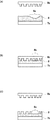
図5は光硬化樹脂が完全に充填された場合のパターン転写の様子を示す断面模式図である。図5(A)では、光硬化樹脂8の均一塗布された被転写物用基板7bをスタンパ9a(図5では図示せず)の上に載置した転写ステージ16が、転写プレス18のスタンパ9bの下へと移動する。図5(B)では、転写プレス18が下降して、光硬化樹脂8の塗布された被転写物用基板7bを押圧すると同時にUV光源17b(図5では図示せず)によって光硬化樹脂8が硬化する。これによって、スタンパ9bの各パターンが被転写物用基板7bの光硬化樹脂8に転写される。図5(C)では、パターン転写後、転写プレス18のスタンパ9bが上昇することによりスタンパ9bから被転写物用基板7bが剥離される。このような一連の処理によって未充填部分のない光硬化樹脂8が被転写物用基板7bの表面に形成される。
FIG. 5 is a schematic cross-sectional view showing a state of pattern transfer when the photo-curing resin is completely filled. In FIG. 5A, the
図6は光硬化樹脂が完全に充填されていない場合のパターン転写の様子を示す断面模式図である。図6(A)に示すように、光硬化樹脂8の塗布が不十分な箇所(膜厚の薄い部分)8aが存在する場合、被転写物用基板7bをスタンパ9a(図6では図示せず)の上に載置した転写ステージ16が、転写プレス18のスタンパ9bの下へと移動する。図6(B)では、転写プレス18のスタンパ9bが下降して、光硬化樹脂8の塗布された被転写物用基板7bを押圧すると同時にUV光源17b(図6では図示せず)によって光硬化樹脂8が硬化する。しかしながら、光硬化樹脂8の塗布が不十分な箇所(膜厚の薄い部分)8aでは、スタンパ9bの押圧によって、パターン内にレジストが充填されず、未充填部分8bが発生し、スタンパ9bのパターンの間に光硬化樹脂8の充填されない転写不良箇所8cが形成される。図6(C)では、パターン転写後、転写プレス18のスタンパ9bが上昇するが光硬化樹脂8には転写不良箇所8cが存在することとなる。このような転写不良箇所は、カメラや光学顕微鏡などの膜厚検査器20にて図4のバースト4に白い網状の模様として観察されることになる。
FIG. 6 is a schematic cross-sectional view showing a state of pattern transfer when the photo-curing resin is not completely filled. As shown in FIG. 6A, when a
図7は本発明に係る被転写物膜厚検査方法の変形例を示す図である。上述の実施の形態では、サーボパターンのバーストを光学顕微鏡のレンズ2で観察する場合について説明したが、この変形例では、ディスク1の内周付近にそれぞれ深さが異なる溝(高さ)又は幅が異なるパターンを用いて膜厚判定用パターンを形成し、そのパターンにおける光硬化樹脂の充填状態を光学顕微鏡のレンズ2で観察して、膜厚を測定するものである。観察する箇所は、図7に示すよう、ディスク1の内周付近であって角度90度間隔の4箇所3e〜3hとする。
FIG. 7 is a view showing a modification of the transferred object film thickness inspection method according to the present invention. In the above-described embodiment, the case where the servo pattern burst is observed with the
図8は図7の被転写物膜厚検査方法で使用するそれぞれ高さの異なる凸部からなる膜厚判定用パターンを用いた例を示す図である。図8(A)は、それぞれ高さの異なる凸部からなる膜厚判定用パターン10a〜10cを備えたスタンパ9bによって押圧転写が行われている状態の断面を模式的に示している。スタンパ9bは、図8(A)に示すように、膜厚が約20nmの時に充填される膜厚測定用パターン10a、約40nmの時に充填される膜厚測定用パターン10b、約60nmの時に充填される膜厚測定用パターン10cの3種類のそれぞれ高さの異なる凸部からなる膜厚判定用パターンを備えており、UV光線による硬化後に膜厚測定用パターン10a〜10cによって形成されたそれぞれ深さの異なる溝の充填状態を光学顕微鏡のレンズ2で観察することによって、その膜厚を目視で判別することができるようになっている。すなわち、膜厚判定用パターンを備えたスタンパ9bを押し付けた時、膜厚判定用パターン10aの間に形成された溝に樹脂が充填されていれば約20nm、また膜厚判定用パターン10bの間に形成された溝にも樹脂が充填されていれば約40nm、さらに膜厚判定用パターン10cの間に形成された溝にも樹脂が充填されていれば約60nmというように、その膜厚を目視によって容易に測定することができる。
FIG. 8 is a diagram showing an example using a film thickness determination pattern made up of convex portions having different heights, which are used in the transfer object film thickness inspection method of FIG. FIG. 8A schematically shows a cross section in a state where the pressure transfer is performed by the
図9は図7の被転写物膜厚検査方法で使用するそれぞれ幅の異なる凸部からなる膜厚判定用パターンを用いた例を示す図である。図8の膜厚判定用パターン10a〜10cは、それぞれ高さの異なる凹部(深さが異なる溝)のパターンを用いて膜厚を測定する場合について説明したが、図9の膜厚測定用パターン10d〜10fは、それぞれ幅が異なる凸部から膜厚判定用パターンを用いて膜厚を測定するようにしたものである。
FIG. 9 is a diagram illustrating an example using a film thickness determination pattern including convex portions having different widths, which are used in the transferred object film thickness inspection method of FIG. Although the film
図9(A)は、それぞれ幅の異なる凸部からなる膜厚判定用パターン10d〜10fを備えたスタンパ9cによって押圧転写が行われている状態の断面を模式的に示している。スタンパ9cは、図9(A)に示すように、それぞれ幅の異なる3種類の凸部を備えており、UV光線による硬化後に膜厚測定用パターン10d〜10fによって形成されたそれぞれ深さの異なる溝の充填状態を光学顕微鏡のレンズ2で観察することによって、その膜厚を目視で判別することができるようになっている。すなわち、膜厚判定用パターンを備えたスタンパ9cを押し付けた時、膜厚判定用パターン10fの間に形成された溝に樹脂が充填されていれば約20nm、また膜厚判定用パターン10eの間に形成された溝にも樹脂が充填されていれば約40nm、さらに膜厚判定用パターン10dの間に形成された溝にも樹脂が充填されていれば約60nm、というように、その膜厚を目視によって簡易に測定することができる。図8及び図9に示すような膜厚判定用パターンを用いることによって、専用の機器を用いることなく、通常の光学顕微鏡などで数ヶ所の充填状態を観察するだけで膜厚の判定を行うことができる。なお、この実施の形態では、ディスク1の内周付近に膜厚判定用パターンを形成する場合について説明したが、これ以外の箇所に設けてもよいことは言うまでもない。そのパターンにおける光硬化樹脂の充填状態を光学顕微鏡のレンズ2で観察して、膜厚を測定するものである。観察する箇所は、図7に示すよう、ディスク1の内周付近であって角度90度間隔の4箇所3e〜3hとするのが好ましい。
FIG. 9A schematically shows a cross section in a state where the pressure transfer is performed by the
この発明の実施例によれば、専用の測定機器を用いず、ディスク表面上の数箇所を観察するだけで膜厚の判定が可能になり、測定に必要な時間を大幅に削減し、かつその情報を即時フィードバックできるという効果がある。また、オンラインでレジスト膜厚が測定でき、スループットを向上させることができるという効果もある。さらに、本発明によれば、レジスト膜厚の測定の他に、(1)ディスクとスタンパの密着不良、(2)塗布機器の異常、(3)スタンパの変形を確認する事ができる。例えば、4か所確認し、その1か所のみが未充填である場合は前記(1)又は(2)の可能性が高く、2〜3か所が未充填、または連続して同じ位置に未充填がある場合は前記(1)の可能性が高く、同一条件で転写していたにも関わらず、4か所全てが未充填になっていた場合は前記(3)の可能性が高いという、判定をすることが可能となる。 According to the embodiment of the present invention, it becomes possible to determine the film thickness by observing only a few points on the disk surface without using a dedicated measuring instrument, and the time required for measurement is greatly reduced. There is an effect that information can be immediately fed back. In addition, the resist film thickness can be measured online, and the throughput can be improved. Furthermore, according to the present invention, in addition to the measurement of the resist film thickness, (1) poor adhesion between the disc and the stamper, (2) abnormality of the coating device, and (3) deformation of the stamper can be confirmed. For example, if four places are confirmed and only one of them is unfilled, there is a high possibility of the above (1) or (2), and two to three places are unfilled or continuously in the same position. If there is unfilled, the possibility of (1) is high. If all four places are unfilled even though the transfer was performed under the same conditions, the possibility of (3) is high. It is possible to make a determination.
1…ディスク、
10a,10b,10c…膜厚判定用パターン、
12…ローダ、
13…ディスク置き台、
14…ディスクマテハン、
15…スピンコータ、
16…転写ステージ、
17a,17b…UV光源、
18…転写プレス、
19…剥離ステージ、
20…膜厚検査器
2…レンズ、
21…アンローダ、
3…サーボパターン、
4…バースト、
5…グレーゾーン、
6…プレアンビル、
7a,7b…被転写物用基板、
8…光硬化樹脂、
8b…未充填部分、
8c…転写不良箇所、
9a,9b…スタンパ
1 ... disc,
10a, 10b, 10c ... pattern for film thickness determination,
12 ... loader,
13: Disc holder,
14 ... disc material handling,
15 ... Spin coater,
16 ... Transcription stage,
17a, 17b ... UV light source,
18 ... Transfer press,
19 ... Peeling stage,
20 ...
21 ... Unloader,
3. Servo pattern,
4 ... burst,
5 ... Gray zone,
6 ... Pleanville,
7a, 7b ... substrate for transferred object,
8 ... light curable resin,
8b: Unfilled part,
8c ... transfer failure place,
9a, 9b ... Stamper
Claims (10)
前記光硬化樹脂剤に所定のパターンの設けられたスタンパを押圧するステップと、
前記光硬化樹脂剤にUV光線を照射するステップと、
前記UV光線の照射によって硬化した前記光硬化樹脂から前記スタンパを剥離するステップと、
前記スタンパ剥離後に前記光硬化樹脂剤に転写された前記パターンの所定箇所を観察し、前記光硬化樹脂剤の膜厚が適切であるか否かを判断するステップとを含むことを特徴とする被転写物製造方法。 Applying a photo-curing resin agent to the substrate for transfer;
Pressing a stamper provided with a predetermined pattern on the photocurable resin agent;
Irradiating the photocurable resin agent with UV light;
Peeling the stamper from the photocured resin cured by irradiation with the UV light;
Observing a predetermined portion of the pattern transferred to the photo-curing resin agent after the stamper is peeled off, and determining whether or not the film thickness of the photo-curing resin agent is appropriate. Transcript production method.
前記光硬化樹脂剤に前記被転写物用基板固有のパターン及び膜厚測定用パターンの設けられたスタンパを押圧するステップと、
前記光硬化樹脂剤にUV光線を照射するステップと、
前記UV光線の照射によって硬化した前記光硬化樹脂から前記スタンパを剥離するステップと、
前記スタンパ剥離後に前記光硬化樹脂剤に転写された前記膜厚測定用パターンを観察し、前記膜厚測定用パターン内に前記光硬化樹脂が充填されているか否かによって、前記光硬化樹脂剤の膜厚を測定するステップとを含むことを特徴とする被転写物製造方法。 Applying a photo-curing resin agent to the substrate for transfer;
Pressing a stamper provided with a pattern specific to the substrate for transfer object and a film thickness measurement pattern on the photocurable resin agent;
Irradiating the photocurable resin agent with UV light;
Peeling the stamper from the photocured resin cured by irradiation with the UV light;
The film thickness measurement pattern transferred to the photo-curing resin agent after the stamper peeling is observed, and depending on whether the photo-curing resin is filled in the film thickness measurement pattern or not, And a step of measuring a film thickness.
前記樹脂剤塗布手段によって前記被転写物用基板に塗布された前記光硬化樹脂剤に所定のパターンの設けられたスタンパを押圧すると共に前記光硬化樹脂剤にUV光線を照射して前記光硬化樹脂剤を硬化させるパターン転写手段と、
硬化した前記光硬化樹脂剤から前記スタンパを剥離する剥離手段と、
前記スタンパ剥離後に前記光硬化樹脂剤に転写された前記パターンの所定箇所を観察し、前記光硬化樹脂剤の膜厚が適切であるか否かを判断する膜厚判断手段と
を備えたことを特徴とする被転写物製造装置。 A resin agent applying means for applying a photo-curing resin agent to the substrate for transfer;
The photocurable resin agent is applied by pressing a stamper provided with a predetermined pattern on the photocurable resin agent applied to the substrate for transfer object by the resin agent applying means and irradiating the photocurable resin agent with UV light. Pattern transfer means for curing the agent;
Peeling means for peeling the stamper from the cured photocurable resin agent;
A film thickness judging means for observing a predetermined portion of the pattern transferred to the photocurable resin agent after the stamper peeling and judging whether or not the film thickness of the photocurable resin agent is appropriate. An apparatus for manufacturing a transferred object.
前記樹脂剤塗布手段によって前記被転写物用基板に塗布された前記光硬化樹脂剤に前記被転写物用基板固有のパターン及び膜厚測定用パターンの設けられたスタンパを押圧すると共に前記光硬化樹脂剤にUV光線を照射して前記光硬化樹脂剤を硬化させるパターン転写手段と、
硬化した前記光硬化樹脂剤から前記スタンパを剥離する剥離手段と、
前記スタンパ剥離後に前記光硬化樹脂剤に転写された前記膜厚測定用パターンを観察し、前記膜厚測定用パターン内に前記光硬化樹脂が充填されているか否かによって、前記光硬化樹脂剤の膜厚を測定する膜厚測定手段と
を備えたことを特徴とする被転写物製造装置。 A resin agent applying means for applying a photo-curing resin agent to the substrate for transfer;
A stamper provided with a pattern unique to the substrate for transferred object and a pattern for measuring film thickness is pressed against the photocurable resin agent applied to the substrate for transferred object by the resin agent applying means and the photocurable resin Pattern transfer means for curing the photocurable resin agent by irradiating the agent with UV light;
Peeling means for peeling the stamper from the cured photocurable resin agent;
The film thickness measurement pattern transferred to the photo-curing resin agent after the stamper peeling is observed, and depending on whether the photo-curing resin is filled in the film thickness measurement pattern or not, And a film thickness measuring means for measuring the film thickness.
Priority Applications (2)
| Application Number | Priority Date | Filing Date | Title |
|---|---|---|---|
| JP2011104259A JP2012234603A (en) | 2011-05-09 | 2011-05-09 | Method for inspecting film thickness of transferred object, method for producing transferred object, apparatus for producing transferred object, and stamper for transfer |
| PCT/JP2012/061679 WO2012153708A1 (en) | 2011-05-09 | 2012-05-07 | Inspection method for film thickness of transfer-receiving object, manufacturing method for transfer-receiving object, manufacturing device for transfer-receiving object, and stamper for transfer |
Applications Claiming Priority (1)
| Application Number | Priority Date | Filing Date | Title |
|---|---|---|---|
| JP2011104259A JP2012234603A (en) | 2011-05-09 | 2011-05-09 | Method for inspecting film thickness of transferred object, method for producing transferred object, apparatus for producing transferred object, and stamper for transfer |
Publications (1)
| Publication Number | Publication Date |
|---|---|
| JP2012234603A true JP2012234603A (en) | 2012-11-29 |
Family
ID=47139187
Family Applications (1)
| Application Number | Title | Priority Date | Filing Date |
|---|---|---|---|
| JP2011104259A Pending JP2012234603A (en) | 2011-05-09 | 2011-05-09 | Method for inspecting film thickness of transferred object, method for producing transferred object, apparatus for producing transferred object, and stamper for transfer |
Country Status (2)
| Country | Link |
|---|---|
| JP (1) | JP2012234603A (en) |
| WO (1) | WO2012153708A1 (en) |
Cited By (1)
| Publication number | Priority date | Publication date | Assignee | Title |
|---|---|---|---|---|
| JP2015500547A (en) * | 2011-12-05 | 2015-01-05 | シーゲイト テクノロジー エルエルシー | Optical calibration disc |
Citations (3)
| Publication number | Priority date | Publication date | Assignee | Title |
|---|---|---|---|---|
| JP2007059006A (en) * | 2005-08-25 | 2007-03-08 | Tdk Corp | Method for manufacturing original disk, method for manufacturing stamper and method for manufacturing magnetic recording medium |
| JP2011061165A (en) * | 2009-09-14 | 2011-03-24 | Canon Inc | Imprint apparatus and method of manufacturing article |
| JP2011081902A (en) * | 2010-12-08 | 2011-04-21 | Toshiba Corp | Method of manufacturing magnetic recording medium |
-
2011
- 2011-05-09 JP JP2011104259A patent/JP2012234603A/en active Pending
-
2012
- 2012-05-07 WO PCT/JP2012/061679 patent/WO2012153708A1/en not_active Ceased
Patent Citations (3)
| Publication number | Priority date | Publication date | Assignee | Title |
|---|---|---|---|---|
| JP2007059006A (en) * | 2005-08-25 | 2007-03-08 | Tdk Corp | Method for manufacturing original disk, method for manufacturing stamper and method for manufacturing magnetic recording medium |
| JP2011061165A (en) * | 2009-09-14 | 2011-03-24 | Canon Inc | Imprint apparatus and method of manufacturing article |
| JP2011081902A (en) * | 2010-12-08 | 2011-04-21 | Toshiba Corp | Method of manufacturing magnetic recording medium |
Cited By (1)
| Publication number | Priority date | Publication date | Assignee | Title |
|---|---|---|---|---|
| JP2015500547A (en) * | 2011-12-05 | 2015-01-05 | シーゲイト テクノロジー エルエルシー | Optical calibration disc |
Also Published As
| Publication number | Publication date |
|---|---|
| WO2012153708A1 (en) | 2012-11-15 |
Similar Documents
| Publication | Publication Date | Title |
|---|---|---|
| US5526341A (en) | Test disk having defect patterns uniformly distributed in recording areas | |
| JP5175605B2 (en) | Pattern shape inspection method | |
| US20080237938A1 (en) | Method for manufacturing information recording medium, method of transferring concavo-convex pattern, and transfer apparatus | |
| JP2012234603A (en) | Method for inspecting film thickness of transferred object, method for producing transferred object, apparatus for producing transferred object, and stamper for transfer | |
| US8142693B2 (en) | Stamper and stamper evaluation method | |
| JP4630929B2 (en) | Stamper evaluation method | |
| TWI606443B (en) | Optical calibration discs | |
| US7888930B2 (en) | Method for testing mold structure and magnetic recording medium | |
| JP2008116272A (en) | Pattern inspection method and pattern inspection apparatus | |
| TWI254306B (en) | Manufacturing method of stamper for manufacturing data medium, the stamper, and the photoresist template | |
| JP6668714B2 (en) | Injection mold release test method | |
| JP5548151B2 (en) | Pattern shape inspection method and apparatus | |
| JP4861505B2 (en) | Stamper evaluation method | |
| JP2010192111A (en) | Stamper and evaluation method of stamper | |
| JP4629780B2 (en) | Test optical disc manufacturing method and test optical disc manufacturing apparatus | |
| JP6508306B2 (en) | Inspection method for imprint substrate, imprint method and imprint system | |
| JP2005201785A (en) | Method for detecting mixed-in bubbles, detection apparatus, and duplication method | |
| CN100339681C (en) | CD detection device | |
| JP5358674B2 (en) | Multilayer information recording medium manufacturing method, multilayer information recording medium manufacturing apparatus, and multilayer information recording medium | |
| JP2010003360A (en) | Quality check method and resin mold manufacturing method | |
| JP2004259339A (en) | Inspection device for magnetic transfer master carrier | |
| JP2776205B2 (en) | Inspection disk and manufacturing method thereof | |
| EP2091043A1 (en) | A method for examining an optical stamper | |
| CN101627432B (en) | Master disk, master disk manufacturing method, stamper, disk substrate, optical disk, and optical disk manufacturing method | |
| JP2011237255A (en) | Device and method for detecting pattern profile, and production line for patterned media disk |
Legal Events
| Date | Code | Title | Description |
|---|---|---|---|
| A621 | Written request for application examination |
Free format text: JAPANESE INTERMEDIATE CODE: A621 Effective date: 20140325 |
|
| A131 | Notification of reasons for refusal |
Free format text: JAPANESE INTERMEDIATE CODE: A131 Effective date: 20140826 |
|
| A02 | Decision of refusal |
Free format text: JAPANESE INTERMEDIATE CODE: A02 Effective date: 20150106 |