JP2012190885A - Semiconductor device and method for manufacturing the same - Google Patents
Semiconductor device and method for manufacturing the same Download PDFInfo
- Publication number
- JP2012190885A JP2012190885A JP2011051224A JP2011051224A JP2012190885A JP 2012190885 A JP2012190885 A JP 2012190885A JP 2011051224 A JP2011051224 A JP 2011051224A JP 2011051224 A JP2011051224 A JP 2011051224A JP 2012190885 A JP2012190885 A JP 2012190885A
- Authority
- JP
- Japan
- Prior art keywords
- land
- wiring
- connection conductor
- base
- width
- Prior art date
- Legal status (The legal status is an assumption and is not a legal conclusion. Google has not performed a legal analysis and makes no representation as to the accuracy of the status listed.)
- Pending
Links
Images


Classifications
-
- H—ELECTRICITY
- H10—SEMICONDUCTOR DEVICES; ELECTRIC SOLID-STATE DEVICES NOT OTHERWISE PROVIDED FOR
- H10W—GENERIC PACKAGES, INTERCONNECTIONS, CONNECTORS OR OTHER CONSTRUCTIONAL DETAILS OF DEVICES COVERED BY CLASS H10
- H10W72/00—Interconnections or connectors in packages
- H10W72/01—Manufacture or treatment
- H10W72/012—Manufacture or treatment of bump connectors, dummy bumps or thermal bumps
Landscapes
- Internal Circuitry In Semiconductor Integrated Circuit Devices (AREA)
Abstract
【課題】配線の断線を防止する。
【解決手段】半導体装置1が、半導体基板11と、半導体基板11の上に形成された配線21と、半導体基板11の上に形成され、配線21に接続された接続導体22と、半導体基板11の上に形成され、接続導体22に接続されたランド23と、ランド23の上に形成され、ランド23の外縁からはみ出るように形成された端子29と、を備る。接続導体22が端子29の外周からはみ出て、接続導体22の幅W2が配線21の幅W1よりも広い。
【選択図】図2An object of the present invention is to prevent disconnection of wiring.
A semiconductor device includes a semiconductor substrate, a wiring formed on the semiconductor substrate, a connection conductor formed on the semiconductor substrate and connected to the wiring, and a semiconductor substrate. A land 23 connected to the connection conductor 22, and a terminal 29 formed on the land 23 so as to protrude from the outer edge of the land 23. The connection conductor 22 protrudes from the outer periphery of the terminal 29, and the width W 2 of the connection conductor 22 is wider than the width W 1 of the wiring 21.
[Selection] Figure 2
Description
本発明は、半導体装置及びその製造方法に関する。 The present invention relates to a semiconductor device and a manufacturing method thereof.
半導体チップのパッケージ方法として、いわゆるWLP(Wafer Level Package)法がある。WLP法は、個片化する前の半導体ウエハに配線形成と樹脂封止を行った後に、チップサイズに切り出す方法である(例えば、特許文献1の図1〜図2参照)。具体的には、以下のような工程を経て、半導体チップをパッケージする。即ち、まず、シード層(9)を半導体ウエハの表面に成長させる。その後、そのシード層(9)をレジスト(16)によってマスキングした状態で、そのシード層(9)の上に配線(10)を電解メッキ法により形成する。そのレジスト(16)の除去後、ドライフィルム(19)を貼り付けて、そのドライフィルム(19)に開口(12)を形成する。次に、ドライフィルム(19)の開口(12)内に柱状電極(11)を電解メッキ法によって成長させる。そのドライフィルム(19)の除去後、エポキシ樹脂を塗布して、エポキシ樹脂で配線(10)及び柱状電極(11)を覆い、そのエポキシ樹脂を硬化させる。エポキシ樹脂が硬化することで封止層(14)になる。その後、封止層(14)の表面を研削し、柱状電極(11)を露出させる。次に、その柱状電極(11)の表面にバンプ(15)を形成し、最後に半導体ウエハを封止層(14)と一緒に個片化する。 As a semiconductor chip packaging method, there is a so-called WLP (Wafer Level Package) method. The WLP method is a method of cutting a chip size after wiring formation and resin sealing are performed on a semiconductor wafer before singulation (see, for example, FIGS. 1 to 2 of Patent Document 1). Specifically, the semiconductor chip is packaged through the following steps. That is, first, the seed layer (9) is grown on the surface of the semiconductor wafer. Thereafter, with the seed layer (9) masked by the resist (16), a wiring (10) is formed on the seed layer (9) by an electrolytic plating method. After removing the resist (16), a dry film (19) is attached to form an opening (12) in the dry film (19). Next, the columnar electrode (11) is grown in the opening (12) of the dry film (19) by an electrolytic plating method. After the dry film (19) is removed, an epoxy resin is applied, the wiring (10) and the columnar electrode (11) are covered with the epoxy resin, and the epoxy resin is cured. The epoxy resin is cured to form the sealing layer (14). Thereafter, the surface of the sealing layer (14) is ground to expose the columnar electrode (11). Next, bumps (15) are formed on the surface of the columnar electrode (11), and finally the semiconductor wafer is separated into pieces together with the sealing layer (14).
ところで、特許文献1には、配線(10)の平面的な形状について何ら記載されていない。配線(10)の幅が柱状電極(11)の直径よりも狭いと、配線(10)のうち柱状電極(11)の外周を横切る箇所に電力集中が生じる。そのため、配線(10)は、柱状電極(11)の外周を横切る箇所で断線してしまうことがある。
また、電気めっきにより柱状電極(11)を形成する際、ドライフィルム(19)を用いている。そして、シード層(9)の上面には配線(10)が形成されているので、配線(10)およびシード層(9)の上面にドライフィルム(19)をラミネートすることになる。ところで、最近では、狭ピッチ化の進行に伴い、配線(10)のランドと配線(10)の引き回し線部との間隔が狭くなってきている。配線(10)のランドの直径は柱状電極(11)の直径よりも例えば数μm〜10μm大きくなっている。また、配線(10)の厚さは例えば6μm程度と比較的厚くなっている。
この結果、ラミネートローラを用いた熱圧着方法では、ローラ圧力が配線(10)のランドと配線(10)の引き回し線部との間に十分に伝わらず、配線(10)のランドの周辺部上面へのドライフィルムの密着性が低下し、メッキ液が配線(10)のランドと配線(10)の引き回し線部との間に染み出し、シード層(9)のエッチング工程においてシード層(9)のエッチング不良が発生し、配線(10)間でショートが発生してしまうことがある。
そこで、本発明が解決しようとする課題は、ドライフィルム(19)の密着性の低下によるメッキ液の染み出しが起こりにくいようにすると共に、配線の断線を防止することである。
Incidentally, Patent Document 1 does not describe anything about the planar shape of the wiring (10). If the width of the wiring (10) is narrower than the diameter of the columnar electrode (11), power concentration occurs in the wiring (10) at a location crossing the outer periphery of the columnar electrode (11). For this reason, the wiring (10) may be disconnected at a location crossing the outer periphery of the columnar electrode (11).
Further, when the columnar electrode (11) is formed by electroplating, a dry film (19) is used. Since the wiring (10) is formed on the upper surface of the seed layer (9), the dry film (19) is laminated on the upper surfaces of the wiring (10) and the seed layer (9). Recently, with the progress of narrowing the pitch, the distance between the land of the wiring (10) and the lead line portion of the wiring (10) has become narrower. The diameter of the land of the wiring (10) is, for example, several μm to 10 μm larger than the diameter of the columnar electrode (11). Further, the thickness of the wiring (10) is relatively thick, for example, about 6 μm.
As a result, in the thermocompression bonding method using the laminate roller, the roller pressure is not sufficiently transmitted between the land of the wiring (10) and the lead wire portion of the wiring (10), and the upper surface of the peripheral portion of the land of the wiring (10) The adhesion of the dry film to the surface decreases, and the plating solution oozes out between the land of the wiring (10) and the lead line portion of the wiring (10), and the seed layer (9) is etched in the seed layer (9) etching process. May cause a short circuit between the wirings (10).
Accordingly, the problem to be solved by the present invention is to prevent the plating solution from leaking out due to a decrease in the adhesion of the dry film (19) and to prevent the wiring from being disconnected.
以上の課題を解決するための本発明に係る半導体装置が、半導体基板と、前記半導体基板の上方に設けられた配線と、一端部が、前記配線の一端部に接続された接続導体と、前記接続導体の他端部に接続され、平面視して前記配線の幅より広い幅のランドと、前記ランド上及び前記ランドの周側面の少なくとも一部を覆うように設けられた端子と、を備えている。 In order to solve the above problems, a semiconductor device according to the present invention includes a semiconductor substrate, a wiring provided above the semiconductor substrate, a connection conductor having one end connected to one end of the wiring, A land connected to the other end of the connection conductor and having a width wider than the width of the wiring in plan view; and a terminal provided to cover at least a part of the land and the peripheral side surface of the land. ing.
本発明に係る半導体装置の製造方法は、配線と、前記配線の一端部に、一端部が接続された接続導体と、前記接続導体の他端部に接続され、平面視して前記配線の幅より広い幅のランドと、を半導体ウエハの上方に形成し、前記ランド上及び前記ランドの周側面を覆うように端子を形成する方法である。 The method for manufacturing a semiconductor device according to the present invention includes a wiring, a connection conductor having one end connected to one end of the wiring, and the width of the wiring in plan view, connected to the other end of the connection conductor. In this method, a land having a wider width is formed above a semiconductor wafer, and a terminal is formed so as to cover the land and the peripheral side surface of the land.
本発明によれば、配線の断線を防止することができる。 According to the present invention, disconnection of wiring can be prevented.
以下に、本発明を実施するための形態について、図面を用いて説明する。但し、以下に述べる実施形態には、本発明を実施するために技術的に好ましい種々の限定が付されているが、本発明の範囲を以下の実施形態及び図示例に限定するものではない。 EMBODIMENT OF THE INVENTION Below, the form for implementing this invention is demonstrated using drawing. However, the embodiments described below are given various technically preferable limitations for carrying out the present invention, but the scope of the present invention is not limited to the following embodiments and illustrated examples.
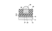
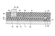
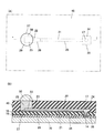
図1は、半導体装置1の一部を破断した状態で示した斜視図である。図2(A)は、この半導体装置1に設けられた導体構造20の平面図である。図2(B)は、図2(A)の導体構造20のうち、アウター端子29を形成する前の配線21、接続導体22、ランド23の平面図である。図3は、III−III断面図である。図4は、IV−IV断面図である。
FIG. 1 is a perspective view showing a part of the semiconductor device 1 in a broken state. FIG. 2A is a plan view of the
図1に示すように、半導体装置1は、チップサイズにパッケージしたものであって、いわゆるCSP(Chip Size Package)である。特に、この半導体装置1は、個片化する前の半導体ウエハの表面を樹脂によって封止した後に、それをチップサイズに個片化したものである。つまり、半導体装置1は、CSPの中でも特にWLP(Wafer Level Package)である。 As shown in FIG. 1, the semiconductor device 1 is packaged in a chip size and is a so-called CSP (Chip Size Package). In particular, the semiconductor device 1 is obtained by sealing the surface of a semiconductor wafer before being singulated with a resin and then singulating it into chips. That is, the semiconductor device 1 is a WLP (Wafer Level Package) among CSPs.
半導体装置1は、半導体基板11、パッシベーション膜15、絶縁膜16、導体構造20、封止層40及び半田バンプ50を有する。
The semiconductor device 1 includes a
半導体基板11は、半導体ウエハを個片化したものである。半導体基板11は、一方の面12と、その面12の反対側となる他方の面13と、これら面12,13の間の厚みと、を有する。半導体基板11は、シリコンといった半導体材料等からなる。半導体基板11の表側の表層には、集積回路が形成されている。
The
半導体基板11の一方の面12がパッシベーション膜15によって被覆されている。半導体基板11の表層に形成された集積回路がパッシベーション膜15によって保護されている。パッシベーション膜15は、酸化シリコン又は窒化シリコンを含有する。パッシベーション膜15が、絶縁膜16によって被覆されている。絶縁膜16は、エポキシ系樹脂、ポリイミド系樹脂その他の樹脂を含有する。例えば、絶縁膜16には、ポリイミド(PI)、ポリベンゾオキサゾール(PBO)、エポキシ系、フェノール系、シリコン系等のプラスチック材料又はこれらの複合材料等を用いることができる。なお、絶縁膜16が形成されていなくてもよい。
One
半導体基板11の一方の面12には、複数のインナー端子14が形成されている。インナー端子14は、半導体基板11の表層に形成された集積回路の配線の一部であったり、その集積回路の各種電気素子(例えば、ダイオード、トランジスタ、抵抗、コンデンサ等)の電極であったりする。パッシベーション膜15及び絶縁膜16のうちインナー端子14に重なる位置には、コンタクトホール17(図2、図4等に図示)が形成されており、インナー端子14の全体又は一部はパッシベーション膜15及び絶縁膜16によって覆われていない。
A plurality of
本実施の形態では、半導体基板11、パッシベーション膜15及び絶縁膜16の積層体が基材である。
In the present embodiment, a laminated body of the
絶縁膜16上(絶縁膜16が無い場合には、パッシベーション膜15上)には、複数の導体構造20が設けられている。導体構造20は、半田バンプ50とインナー端子14を電気的に導通させる。1体の導体構造20に接続されるインナー端子14の数は1又は複数である。1体の導体構造20に接続される半田バンプ50の数は1又は複数である。
A plurality of
図2〜図4に示すように、導体構造20は、配線21、接続導体22、ランド23、インナーランド24、配線下地25、接続導体下地26、ランド下地27、インナーランド下地28及びアウター端子29を有する。
As shown in FIGS. 2 to 4, the
配線下地25、接続導体下地26、ランド下地27及びインナーランド下地28は、絶縁膜16の開口内以外は絶縁膜16上(絶縁膜16が無い場合には、パッシベーション膜15上)に敷設されている。配線下地25は線状に設けられ、平面視した配線下地25の幅W1(配線下地25の長さ方向に対して直行する方向の長さ)がほぼ一様である。配線下地25は、直線状又は曲線状である。
The
接続導体下地26が配線下地25の端部に接続され、インナーランド下地28が配線下地25の別の端部に接続されている。ランド下地27が、接続導体下地26と配線下地25との接続部の反対側で、接続導体下地26に接続されている。配線下地25、接続導体下地26、ランド下地27及びインナーランド下地28は、一体形成されている。配線下地25、接続導体下地26、ランド下地27及びインナーランド下地28は導体である。配線下地25、接続導体下地26、ランド下地27及びインナーランド下地28は、銅(Cu)の薄膜、チタン(Ti)の薄膜、チタンに銅を積層した薄膜その他の金属薄膜である。
The connecting
インナーランド下地28の一部がコンタクトホール17に埋まり、インナーランド下地28の一部がインナー端子14上に形成され、インナーランド下地28とインナー端子14が電気的に導通している。インナーランド下地28の面積がコンタクトホール17の開口面積よりも大きく、インナーランド下地28の縁寄り部分がコンタクトホール17の周囲で絶縁膜16上(絶縁膜16が無い場合には、パッシベーション膜15上)に形成されている。インナーランド下地28の直径(インナーランド下地28が円形でない場合には、インナーランド下地28の外接円の直径)は、配線下地25の幅W1よりも長い。
A part of the
接続導体下地26が三角形状に形作られ、三角形の何れかの頂部が配線下地25の端部に接続されている。接続導体下地26は、配線下地25の延長線25aから両側に膨出するように設けられ、平面視した接続導体下地26の幅W2は配線下地25の幅W1よりも広い。接続導体下地26の幅W2は、一様ではない。具体的には、接続導体下地26の幅W2は、ランド下地27側から配線下地25側にかけて漸減する。接続導体下地26の幅W2とは、配線下地25の延長線25aに直交する方向の長さをいう。
The
ランド下地27は、島状に形成されており、より具体的には円形状に形成されている。ランド下地27の周縁部の一部が、接続導体下地26の三角形状の頂部(配線下地25との接続部分)に対する底部に接続されている。ランド下地27と接続導体下地26を組み合わせた形状は、いわゆるティアドロップ型(しずく型)である。なお、ランド下地27が三角形状、四角形状その他の凸多角形状に形成されていてもよい。また、ランド下地27が楕円形状に形成されていてもよい。
The
ランド下地27の直径(インナーランド下地28が円形でない場合には、インナーランド下地28の外接円の直径)は、配線下地25の幅W1よりも長く、更に、接続導体下地26の幅W2(最も広い部分)以上である。
The diameter of the land base 27 (when the
配線21が配線下地25上に形成されている。接続導体22が接続導体下地26上に形成されている。ランド23がランド下地27上に形成されている。インナーランド24がインナーランド下地28上に形成されている。
The
配線21は線状に設けられ、配線21の幅W1がほぼ一様である。配線21の平面形状と配線下地25の平面形状が同じであり、平面視して配線21と配線下地25が合致している。配線21の幅W1と配線下地25の幅W1が等しい。
The
接続導体22が配線21の端部に接続され、インナーランド24が配線21の別の端部に接続されている。ランド23が、接続導体22と配線21との接続部の反対側で接続導体22に接続されている。配線21、接続導体22、ランド23及びインナーランド24は、一体形成されている。配線21、接続導体22、ランド23及びインナーランド24は、導体である。配線21、接続導体22、ランド23及びインナーランド24は、銅メッキその他の金属メッキからなる。配線21、接続導体22、ランド23及びインナーランド24は、配線下地25、接続導体下地26、ランド下地27及びインナーランド下地28よりも厚い。
The
インナーランド24がインナーランド下地28を介してインナー端子14に電気的導通している。インナーランド24の面積がコンタクトホール17の開口面積よりも大きく、インナーランド24の縁寄り部分がインナーランド下地28を介して絶縁膜16上(絶縁膜16が無い場合には、パッシベーション膜15上)に形成されている。インナーランド24の直径(インナーランド24が円形でない場合には、インナーランド24の外接円の直径)は、配線21及び配線下地25の幅W1よりも長い。インナーランド24の平面形状がインナーランド下地28の平面形状と同じであり、インナーランド24の周縁とインナーランド下地28の周縁が重なっている。
The
接続導体22が三角形状に形作られ、三角形の何れかの頂部が配線21の端部に接続されている。接続導体22は、配線21の延長線25aから両側に膨出するように設けられ、接続導体22の幅W2は配線21の幅W1よりも広い。接続導体22の幅W2は、一様ではない。具体的には、接続導体22の幅W2は、ランド23側から配線21側に向かって漸減する。接続導体22の幅W2とは、配線21の延長線25aに直交する方向の長さをいう。
The
接続導体22の平面形状が接続導体下地26の平面形状と同じであり、接続導体22の周縁と接続導体下地26の周縁が重なっている。
The planar shape of the
ランド23は、島状に形成されており、より具体的には矩形状に形成されている。ランド23の周縁部の一部が、接続導体22の三角形状の頂部(配線21との接続部分)に対する底部に接続されている。なお、ランド23が三角形状、四角形状その他の凸多角形状に形成されていてもよい。また、ランド23が円形又は楕円形に形成されていてもよい。
The
ランド23の面積がランド下地27の面積よりも狭い。平面視して、ランド23全体がランド下地27の外縁の内側に配置され、ランド下地27の外縁寄り部分がランド23の外縁からはみ出ている。ランド23の外縁のうち接続導体22との接続部分以外は、ランド下地27の外縁から内側に離れている。ランド23の幅W3(ランド23の延長線25aに直交する方向の長さをいう。)は、配線21の幅W1よりも広い。また、ランド23が円形の場合は、ランド23の内接円の直径をW3とする。ランド23の幅W3は、配線21側からランド23側にかけて漸増していく際の最も広い部分の接続導体22の幅W2と同じである。
The area of the
アウター端子29は、柱状電極である。アウター端子29は、ランド23及びランド下地27の上に立設されている。つまり、アウター端子29の中央部分がランド23の上に形成され、アウター端子29の外周寄り部分がランド23の外縁から外にはみ出てランド下地27の外縁寄り部分の上に形成されている。アウター端子29の平面形状とランド下地27の平面形状が同じであり、アウター端子29の外周がランド下地27の外縁に重なっている。アウター端子29の高さ(厚さ)は、配線21、接続導体22、ランド23及びインナーランド24の厚さよりも高い。アウター端子29は、銅その他の金属からなる。平面視した際、ランド23全体がアウター端子29と重なっており、ランド23はアウター端子29下に位置する。
The
また、平面視して、接続導体22及び接続導体下地26が、アウター端子29の外周から外にはみ出ている。平面視して、接続導体22及び接続導体下地26が、アウター端子29と重なる領域は存在しない。
Further, the
絶縁膜16上には、封止層40が積層されている。封止層40が、配線21、接続導体22及びインナーランド24を覆っている。配線21、接続導体22、配線下地25、接続導体下地26、ランド下地27及びインナーランド下地28が、絶縁膜16と封止層40の間に介在する。封止層40は、配線21、接続導体22及びインナーランド24をそれらの上から保護する。アウター端子29が封止層40を貫通するように封止層40に埋設されている。アウター端子29の頭頂面は封止層40によって覆われていないが、アウター端子29の周側面は封止層40によって覆われ、封止層40がアウター端子29の周面を保護する。封止層40の表面は、アウター端子29の頭頂面と面一に設けられ、又は、アウター端子29の頭頂面よりも僅かに高い位置にある。封止層40は、エポキシ系樹脂、ポリイミド系樹脂その他の絶縁性樹脂を含有し、好ましくは、絶縁性樹脂(例えば、エポキシ系樹脂又はポリイミド系樹脂)にフィラー(例えば、ガラスフィラー又はシリカフィラー)又は繊維(例えば、ガラス繊維又は炭素繊維)を配合した強化樹脂からなる。また、封止層40は遮光性を有する。
A
半田バンプ50がアウター端子29の頭頂面に形成されている。半田バンプ50がアウター端子29の頭頂面に結合することによって、半田バンプ50とアウター端子29が相互に電気的に接続している。なお、半田バンプ50が無くてもよい。
A
1体の導体構造20に接続されるインナー端子14の数が複数である場合、1体の導体構造20が有するインナーランド24及びインナーランド下地28の数が複数である。その場合、配線21及び配線下地25が分岐しており、分かれたそれぞれの端部ごとにインナーランド24及びインナーランド下地28が接続される。
また、1体の導体構造20に接続される半田バンプ50の数が複数である場合、1体の導体構造20が有する接続導体22、ランド23、接続導体下地26及びランド下地27の数が複数である。その場合、配線21及び配線下地25が分岐しており、分かれたそれぞれの端部ごとに接続導体22及び接続導体下地26が接続される。
When the number of
Further, when the number of solder bumps 50 connected to one
半導体装置1及び導体構造20の製造方法について図5〜図16を参照して説明する。図5〜図16は半導体装置1の製造工程を示すものであり、図5は、半導体装置1の製造に用いる半導体ウエハ70の斜視図であり、図6〜図16の(A)は半導体ウエハ70の要部の平面図であり、(B)はその半導体ウエハ70の要部の断面図である。
A method for manufacturing the semiconductor device 1 and the
半導体装置1を製造するに際しては、個片化する前の半導体ウエハ70(図5に図示)を用いる。図5に示すように、半導体ウエハ70は、分割予定線としての格子状の境界線(ダイシングストリート)72によって複数のチップ領域71に区分けされている。これらチップ領域71がマトリクス状に配列されている。半導体ウエハ70の表層には、チップ領域71ごとに集積回路が形成されている。パッシベーション膜15が半導体ウエハ70の表側の面上に成膜され、集積回路がパッシベーション膜15によって覆われている。パッシベーション膜15はパターニングされており、複数のコンタクトホール17が各チップ領域71内の外周付近のパッシベーション膜15に形成されている。
When the semiconductor device 1 is manufactured, a semiconductor wafer 70 (shown in FIG. 5) before being singulated is used. As shown in FIG. 5, the
まず、パッシベーション膜15の上に絶縁膜16をパターニングすることで、チップ領域71ごとに絶縁膜16を分断するとともに、絶縁膜16に複数のコンタクトホール17を形成する。なお、絶縁膜16のパターニングを省略してもよい。
次に、図6に示すように、無電解メッキ法若しくは気相成長法(例えば、スパッタ法)又はこれらの組合せによって、絶縁膜16(絶縁膜16が無い場合には、パッシベーション膜15)の上及びコンタクトホール17の中にシード層73を成長させる。シード層73は、銅(Cu)の薄膜、チタン(Ti)の薄膜、チタンに銅を積層した薄膜その他の金属薄膜である。
First, the insulating
Next, as shown in FIG. 6, on the insulating film 16 (or the
次に、図7に示すように、シード層73の上にレジスト74の塗布又は貼着をして、そのレジスト74の露光・現像をすることで、そのレジスト74をパターニングする。レジスト74をパターニングすることによって、レジスト74に複数の溝75を形成する。溝75の平面形状は、配線21、接続導体22、ランド23及びインナーランド24を組み合わせた平面形状と同じである。つまり、溝75は、線状部分75aと、線状部分75aの端部に繋がる幅広部75bと、幅広部75bに繋がる大開口部75cと、線状部分75aの別の端部に繋がる小開口部75dとからなる。線状部分75aが配線21に対応し、幅広部75bが接続導体22に対応し、大開口部75cがランド23に対応し、小開口部75dがインナーランド24に対応する。溝75の形成に際しては、小開口部75d内にはコンタクトホール17を位置させる。
Next, as shown in FIG. 7, a resist 74 is applied or stuck on the
次に、図8に示すように、残留したレジスト74をマスクとしてそのレジスト74によってシード層73の一部を被覆した状態で、シード層73を電極として電解メッキを行う。これにより、シード層73の上であってレジスト74の溝75内に配線21、接続導体22、ランド23及びインナーランド24を成長させる。この際、配線21、接続導体22、ランド23及びインナーランド24をシード層73よりも厚く成長させる。配線21は線状部分75a内で成長し、接続導体22は幅広部75b内で成長し、ランド23は大開口部75c内で成長し、インナーランド24が小開口部75d内で成長する。
配線21、接続導体22、ランド23及びインナーランド24の形成後、レジスト74を除去する。
Next, as shown in FIG. 8, using the remaining resist 74 as a mask, electrolytic plating is performed using the
After the
次に、図9に示すように、配線21、接続導体22、ランド23及びインナーランド24よりも厚いネガ型のドライフィルムレジスト76をシード層73、配線21、接続導体22、ランド23及びインナーランド24の上の一面に貼り付ける。なお、ドライフィルムレジスト76を用いる代わりに、液状のネガ型レジストを厚くコーティングしてもよい。また、ドライフィルムレジスト76及び液状レジストがポジ型であってもよい。
Next, as shown in FIG. 9, a negative dry film resist 76 thicker than the
次に、図10に示すように、レクチル77及び露光装置を用いて、ドライフィルムレジスト76を露光する。ドライフィルムレジスト76がネガ型である場合、レクチル77によって遮光する領域78はランド23及びその周辺の上である。ここで、平面視して、遮光領域78の面積をランド23の面積よりも大きくし、ランド23全体を遮光領域78の内側に配置し、ランド23の外縁(但し、ランド23と接続導体22の境界を除く。)を遮光領域78の縁から離す。また、遮光領域78を接続導体22の外側に位置させ、接続導体22を遮光領域78からはみ出させる。遮光領域78の縁がランド23の外縁(但し、ランド23と接続導体22の境界を除く。)から離れているので、ドライフィルムレジスト76に投射された光がランド23の外縁(但し、ランド23と接続導体22の境界を除く。)に入射しない。そのため、光がランド23の表面で乱反射することがない。従って、レクチル77のパターンが、解像不良とならずに、ドライフィルムレジスト76に投影される。シード層73は無電解メッキ又は気相成長法により形成されたものであるから、シード層73の表面に光が入射しても乱反射しにくい。なお、ポジ型のレジストを用いた場合、遮光領域78と露光領域79を反転させる。また、図10では、露光装置の光源や投影光学系の図示を省略する。
Next, as shown in FIG. 10, the dry film resist 76 is exposed using a
次に、図11に示すように、ドライフィルムレジスト76を現像して、ドライフィルムレジスト76に開口80を形成する。開口80は遮光領域78に形成される。平面視して、開口80の面積がランド23の面積よりも大きく、ランド23全体が開口80の内側に配置され、ランド23の外縁(但し、ランド23と接続導体22の境界を除く。)が開口80の縁から離れる。そのため、開口80のうちランド23の周辺部ではシード層73の一部が露出する。形成された開口80の縁がランド23の上でなく、シード層73の上にあり、ランド23が開口80内に配置されている。そのため、ランド23からその近傍の別の配線までの間の領域では、シード層73とドライフィルムレジスト76との間に隙間が発生しにくく、その領域ではドライフィルムレジスト76とシード層73が密着している。また、形成された開口80の縁の一部がランド23と接続導体22の境界に重なる。
Next, as shown in FIG. 11, the dry film resist 76 is developed to form
次に、図12に示すように、残留したドライフィルムレジスト76をマスクとしてそのドライフィルムレジスト76でシード層73、配線21、接続導体22及びインナーランド24を被覆した状態で、シード層73及びランド23等を電極として電解メッキを行う。これにより、ドライフィルムレジスト76の開口80内において、アウター端子29をランド23及びシード層73の上に成長させる。ここで、アウター端子29を配線21、接続導体22、ランド23及びインナーランド24よりも厚く成長させる。
Next, as shown in FIG. 12, with the remaining dry film resist 76 as a mask, the
電解メッキの際、ランド23とその近傍の別の配線との間の領域では、ドライフィルムレジスト76の追従性が向上して、ドライフィルムレジスト76とシード層73が密着しているから、メッキ液がドライフィルムレジスト76とシード層73との間に浸透しない。そのため、アウター端子29がその近傍の別の配線に短絡することを防止することができる。
アウター端子29の形成後、ドライフィルムレジスト76を除去する。
In electrolytic plating, in the region between the
After the formation of the
次に、図13に示すように、シード層73のうち配線21、接続導体22、ランド23、インナーランド24及びアウター端子29に重なっていない部分をエッチングにより除去する。そうすることで、シード層73をパターニングして、シード層73から配線下地25、接続導体下地26、ランド下地27、インナーランド下地28及びアウター端子29を形成する。このとき、配線21、接続導体22、インナーランド24及びアウター端子29の表面が一部エッチングされるが、配線21、接続導体22、インナーランド24及びアウター端子29がシード層73と比較して充分に厚いため、配線21、接続導体22、インナーランド24及びアウター端子29は残留する。
Next, as shown in FIG. 13, portions of the
次に、図14に示すように、印刷法、液滴吐出法(インクジェット法)、スピンコート法、滴下法その他の塗布法によって封止樹脂を絶縁膜16(絶縁膜16が無い場合には、パッシベーション膜15)上に塗布し、その封止樹脂によって配線21、接続導体22、インナーランド24及びアウター端子29を覆って、その封止樹脂を硬化させる。これにより、絶縁膜16(絶縁膜16が無い場合には、パッシベーション膜15)上に封止層40を形成する。封止層40の形成に際しては、封止層40の厚さをアウター端子29の厚さ(高さ)よりも厚くして、アウター端子29全体を封止層40に埋め込む。封止層40は、なお、プリプレグを絶縁膜16(絶縁膜16が無い場合には、パッシベーション膜15)に貼り付けて、そのプリプレグを硬化させて、そのプリプレグから封止層40を形成してもよい。
Next, as shown in FIG. 14, the sealing resin is applied to the insulating film 16 (if the insulating
次に、図15に示すように、封止層40の表面を研削することにより、封止層40の表面がアウター端子29の頭頂面と略面一となるようにアウター端子29の頭頂面を露出させる。この時、アウター端子29の頭頂面も研削され、アウター端子29の頭頂面が平坦になる。
次に、半導体ウエハ70の裏面を研削し、半導体ウエハ70を薄くする。なお、半導体ウエハ70の裏面の研削は、後述の個片化処理時に行ってもよい。
Next, as shown in FIG. 15, the top surface of the
Next, the back surface of the
次に、アウター端子29の頭頂面を軽くエッチングする。この処理は省略してもよい。
次に、図16に示すように、半田バンプ50をアウター端子29の頭頂面に形成する。半田バンプ50の形成は後述の個片化処理の後に行ってもよいし、半田バンプ50を形成しなくてもよい。
次に、封止層40、パッシベーション膜15及び半導体ウエハ70を境界線72(図5参照)に沿って分断することによって、半導体ウエハ70から封止層40までの積層体をチップサイズに細分割する。具体的には、1種類又は複数種類のダイシングブレードによって封止層40、パッシベーション膜15及び半導体ウエハ70を境界線72に沿って切断する。これにより、複数の半導体装置1を得られる。
Next, the top surface of the
Next, as shown in FIG. 16, the
Next, by dividing the
先に半導体ウエハ70の裏面を研削しなかった場合には、半導体ウエハ70の裏面まで切り込むのではなく、ダイシングブレードによって半導体ウエハ70の表側の面と裏面の間の途中まで半導体ウエハ70を切り込む(いわゆる、ハーフダイシング処理)。その後、半導体ウエハ70の裏面を切り込みまで研削すると、半導体ウエハ70を複数の半導体基板11に分断することができる。
If the back surface of the
この実施の形態によれば、以下のような効果が得られる。
(1) 平面視して、細い配線21及び配線下地25がアウター端子29の外周を横切っていない。つまり、配線21及び配線下地25よりも幅広の接続導体22及び接続導体下地26がアウター端子29の外周から外側へはみ出ている。そのため、配線21及び配線下地25の端部からアウター端子29の外周までの部分で電力集中が起こりにくく、断線が生じない。
(2) 図10に示すように、ドライフィルムレジスト76の露光時における遮光領域78がランド23よりも広いから、形成される開口80が解像不良となることがない。つまり、開口80のうち底の部分が遮光領域78よりも狭くならず、ドライフィルムレジスト76がランド23の上に残留しない。一方、従来の技術(特許文献1:特開2008−218731号公報の図2参照)では、ドライフィルム(19)に開口(12)を形成する際には、ドライフィルム(19)を露光・現像し、ドライフイルム(19)の露光に際しては、開口(12)の縁が、露光領域と遮光領域の明暗境界線となる。ところが、配線(10)やその保護金属膜(18)が電解メッキによって形成されているから、配線(10)や保護金属膜(18)の表面が粗いので、露光時の光が配線(10)や保護金属膜(18)の表面で乱反射してしまう。そのため、露光領域と遮光領域の明暗境界線がはっきりせず、ドライフィルム(19)を現像しても、ドライフィルム(19)の一部が開口(12)内に残留してしまう。従って、本発明の実施の形態によれば、従来技術では得ることができない効果を得られる。
(3) 図11に示すように、ランド23の外縁がドライフィルムレジスト76の開口80の縁から内側に離れていることで、アウター端子29をその近傍の他の配線に短絡させずに、アウター端子29を成長させることができる。そのため、アウター端子29を周の他の配線に近づけて形成することができ、単位面積当たりに形成することができるアウター端子29の数を増やすことができる。
(4) 平面視して、ランド23の面積をアウター端子29の面積よりも小さくし、単位面積当たりに形成することができるアウター端子29の数を増やすことができるから、アウター端子29を形成することができる範囲を拡げることができる。
(5) ランド23がアウター端子29の外周からはみ出ていないから、アウター端子29とその近くの配線との距離を長くすることができる。そのため、アウター端子29とその近くの配線との間でイオンマイグレーションが発生することを抑えることができるとともに、アウター端子29とその近くの配線との短絡を防止することができる。
According to this embodiment, the following effects can be obtained.
(1) The
(2) As shown in FIG. 10, since the light-shielding
(3) As shown in FIG. 11, the outer edge of the
(4) Since the area of the
(5) Since the
以下に、この出願の願書に最初に添付した特許請求の範囲に記載した発明を付記する。付記に記載した請求項の項番は、この出願の願書に最初に添付した特許請求の範囲の通りである。 The invention described in the scope of claims attached to the application of this application will be added below. The item numbers of the claims described in the appendix are as set forth in the claims attached to the application of this application.
〔付記〕
<請求項1>
半導体基板と、
前記半導体基板の上方に設けられた配線と、
一端部が、前記配線の一端部に接続された接続導体と、
前記接続導体の他端部に接続され、平面視して前記配線の幅より広い幅のランドと、
前記ランド上及び前記ランドの周側面の少なくとも一部を覆うように設けられた端子と、
を備えていることを特徴とする半導体装置。
<請求項2>
前記接続導体と前記ランドとは、前記半導体基板の上方に設けられており、
平面視して前記接続導体の前記ランド側の端部の幅は、前記接続導体の前記配線側の端部の幅より広いことを特徴とする請求項1に記載の半導体装置。
<請求項3>
前記半導体基板の上方であって前記配線の下に形成された配線下地と、
前記半導体基板の上方であって前記接続導体の下に形成され、前記配線下地に接続された接続導体下地と、
前記半導体基板の上方であって前記ランドの下に形成され、前記接続導体下地に接続されたランド下地と、を更に備え、
前記ランド下地が前記ランドよりも広く形成され、
前記端子のうち前記ランドの外縁からはみ出た部分が前記ランド下地上に設けられ、
前記端子の外周が前記ランド下地の外縁に重なり、
前記接続導体下地が前記端子の外周からはみ出て、
前記配線の幅と前記配線下地の幅が等しく、
前記接続導体下地の幅が前記配線及び前記配線下地の幅よりも広いことを特徴とする請求項1又は2に記載の半導体装置。
<請求項4>
前記接続導体の幅が前記ランド側から前記配線側に向かって漸減し、
前記接続導体下地の幅が前記ランド下地側から前記配線下地側に向かって漸減することを特徴とする請求項3に記載の半導体装置。
<請求項5>
前記端子の周囲において前記半導体基板の上に形成されているとともに前記配線及び前記接続導体を覆う封止層を更に備えることを特徴とする請求項1から4の何れか一項に記載の半導体装置。
<請求項6>
前記端子が前記ランド上に設けられた柱状電極であることを特徴とする請求項1から5の何れか一項に記載の半導体装置。
<請求項7>
配線と、前記配線の一端部に、一端部が接続された接続導体と、前記接続導体の他端部に接続され、平面視して前記配線の幅より広い幅のランドと、を半導体ウエハの上方に形成し、
前記ランド上及び前記ランドの周側面を覆うように端子を形成することを特徴とする半導体装置の製造方法。
<請求項8>
平面視して前記接続導体の前記ランド側の端部の幅は、前記接続導体の前記配線側の端部の幅より広く、
前記接続導体の形成に際しては、前記接続導体の幅を前記ランド側から前記配線側に向かって漸減させることを特徴とする請求項7に記載の半導体装置の製造方法。
<請求項9>
前記配線、前記接続導体及び前記ランドの形成の前に前記半導体ウエハの上にシード層を成膜した後、前記配線、前記接続導体及び前記ランドを前記シード層上に形成し、
前記配線、前記接続導体及び前記ランドの形成の後に前記配線、前記接続導体、前記ランド及び前記シード層をネガ型のレジストで被覆し、前記ランド及びその周辺の上を遮光してその遮光領域から前記接続導体をはみ出させるように前記レジストを露光し、前記レジストを現像することによって前記遮光領域に開口を形成し、
前記端子の形成に際しては、前記ランド及び前記シード層を電極として電解メッキを行って、前記開口内に端子を成長させ、
前記端子の形成後に前記レジストを除去し、
前記シード層のうち前記配線、前記接続導体及び前記端子の重なっていない部分を除去することを特徴とする請求項8に記載の半導体装置の製造方法。
<請求項10>
前記シード層の成膜後に前記シード層の上にレジストをパターニングして、前記シード層を電極として電解メッキを行うことによって前記配線、前記接続導体及び前記ランドを前記シード層上に成長させることを特徴とする請求項9に記載の半導体装置の製造方法。
<請求項11>
前記シード層の部分的な除去後に前記半導体基板の上に封止層を形成して、前記配線、前記接続導体及び前記端子を前記封止層によって覆い、
前記封止層の表面を研削して前記端子を露出させ、
前記封止層及び前記半導体ウエハをチップサイズに分断することを特徴とする請求項89又は10に記載の半導体装置の製造方法。
[Appendix]
<Claim 1>
A semiconductor substrate;
Wiring provided above the semiconductor substrate;
One end part is a connection conductor connected to one end part of the wiring,
Connected to the other end of the connection conductor, and a land having a width wider than the width of the wiring in plan view;
A terminal provided on the land and covering at least a part of the peripheral side surface of the land;
A semiconductor device comprising:
<Claim 2>
The connection conductor and the land are provided above the semiconductor substrate,
2. The semiconductor device according to claim 1, wherein a width of an end portion of the connection conductor on the land side is wider than a width of an end portion of the connection conductor on the wiring side in plan view.
<Claim 3>
A wiring substrate formed above the semiconductor substrate and below the wiring;
A connection conductor base formed above the semiconductor substrate and under the connection conductor, and connected to the wiring base;
A land base formed above the semiconductor substrate and below the land and connected to the connection conductor base; and
The land base is formed wider than the land,
A portion of the terminal that protrudes from the outer edge of the land is provided on the land base,
The outer periphery of the terminal overlaps the outer edge of the land base,
The connection conductor base protrudes from the outer periphery of the terminal,
The width of the wiring and the width of the wiring base are equal,
The semiconductor device according to claim 1, wherein a width of the connection conductor base is wider than a width of the wiring and the wiring base.
<Claim 4>
The width of the connection conductor gradually decreases from the land side toward the wiring side,
4. The semiconductor device according to claim 3, wherein the width of the connection conductor base gradually decreases from the land base side toward the wiring base side.
<Claim 5>
5. The semiconductor device according to claim 1, further comprising a sealing layer formed on the semiconductor substrate around the terminal and covering the wiring and the connection conductor. 6. .
<Claim 6>
The semiconductor device according to claim 1, wherein the terminal is a columnar electrode provided on the land.
<Claim 7>
A wiring, a connection conductor having one end connected to one end of the wiring, and a land connected to the other end of the connection conductor and having a width wider than the width of the wiring in plan view. Forming upwards,
A terminal is formed so as to cover the land and the peripheral side surface of the land.
<Claim 8>
The width of the end portion on the land side of the connection conductor in plan view is wider than the width of the end portion on the wiring side of the connection conductor,
8. The method of manufacturing a semiconductor device according to claim 7, wherein when forming the connection conductor, the width of the connection conductor is gradually reduced from the land side toward the wiring side.
<Claim 9>
After forming a seed layer on the semiconductor wafer before forming the wiring, the connection conductor, and the land, forming the wiring, the connection conductor, and the land on the seed layer,
After forming the wiring, the connection conductor, and the land, the wiring, the connection conductor, the land, and the seed layer are covered with a negative resist, and the land and the periphery thereof are shielded from the light shielding region. Exposing the resist so that the connection conductor protrudes, and developing the resist to form an opening in the light shielding region;
In forming the terminal, electrolytic plating is performed using the land and the seed layer as an electrode, and a terminal is grown in the opening,
Removing the resist after forming the terminal;
The method for manufacturing a semiconductor device according to claim 8, wherein a portion of the seed layer where the wiring, the connection conductor, and the terminal do not overlap is removed.
<Claim 10>
After the seed layer is formed, a resist is patterned on the seed layer, and the wiring, the connection conductor, and the land are grown on the seed layer by performing electrolytic plating using the seed layer as an electrode. The method for manufacturing a semiconductor device according to claim 9, wherein:
<Claim 11>
Forming a sealing layer on the semiconductor substrate after partial removal of the seed layer, covering the wiring, the connection conductor and the terminal with the sealing layer;
Grinding the surface of the sealing layer to expose the terminals;
The method for manufacturing a semiconductor device according to claim 89, wherein the sealing layer and the semiconductor wafer are divided into chip sizes.
1 半導体装置
11 半導体基板
20 導体構造
21 配線
22 接続導体
23 ランド
24 インナーランド
25 配線下地
26 接続導体下地
27 ランド下地
28 インナーランド下地
29 アウター端子
40 封止層
70 半導体ウエハ
73 シード層
74 レジスト
75 溝
75a 線状部分
75b 幅広部
75c 大開口部
75d 小開口部
76 ドライフィルムレジスト
77 レクチル
78 遮光領域
79 露光領域
80 開口
DESCRIPTION OF SYMBOLS 1
Claims (11)
前記半導体基板の上方に設けられた配線と、
一端部が、前記配線の一端部に接続された接続導体と、
前記接続導体の他端部に接続され、平面視して前記配線の幅より広い幅のランドと、
前記ランド上及び前記ランドの周側面の少なくとも一部を覆うように設けられた端子と、
を備えていることを特徴とする半導体装置。 A semiconductor substrate;
Wiring provided above the semiconductor substrate;
One end part is a connection conductor connected to one end part of the wiring,
Connected to the other end of the connection conductor, and a land having a width wider than the width of the wiring in plan view;
A terminal provided on the land and covering at least a part of the peripheral side surface of the land;
A semiconductor device comprising:
平面視して前記接続導体の前記ランド側の端部の幅は、前記接続導体の前記配線側の端部の幅より広いことを特徴とする請求項1に記載の半導体装置。 The connection conductor and the land are provided above the semiconductor substrate,
2. The semiconductor device according to claim 1, wherein a width of an end portion of the connection conductor on the land side is wider than a width of an end portion of the connection conductor on the wiring side in plan view.
前記半導体基板の上方であって前記接続導体の下に形成され、前記配線下地に接続された接続導体下地と、
前記半導体基板の上方であって前記ランドの下に形成され、前記接続導体下地に接続されたランド下地と、を更に備え、
前記ランド下地が前記ランドよりも広く形成され、
前記端子のうち前記ランドの外縁からはみ出た部分が前記ランド下地上に設けられ、
前記端子の外周が前記ランド下地の外縁に重なり、
前記接続導体下地が前記端子の外周からはみ出て、
前記配線の幅と前記配線下地の幅が等しく、
前記接続導体下地の幅が前記配線及び前記配線下地の幅よりも広いことを特徴とする請求項1又は2に記載の半導体装置。 A wiring substrate formed above the semiconductor substrate and below the wiring;
A connection conductor base formed above the semiconductor substrate and under the connection conductor, and connected to the wiring base;
A land base formed above the semiconductor substrate and below the land and connected to the connection conductor base; and
The land base is formed wider than the land,
A portion of the terminal that protrudes from the outer edge of the land is provided on the land base,
The outer periphery of the terminal overlaps the outer edge of the land base,
The connection conductor base protrudes from the outer periphery of the terminal,
The width of the wiring and the width of the wiring base are equal,
The semiconductor device according to claim 1, wherein a width of the connection conductor base is wider than a width of the wiring and the wiring base.
前記接続導体下地の幅が前記ランド下地側から前記配線下地側に向かって漸減することを特徴とする請求項3に記載の半導体装置。 The width of the connection conductor gradually decreases from the land side toward the wiring side,
4. The semiconductor device according to claim 3, wherein the width of the connection conductor base gradually decreases from the land base side toward the wiring base side.
前記ランド上及び前記ランドの周側面を覆うように端子を形成することを特徴とする半導体装置の製造方法。 A wiring, a connection conductor having one end connected to one end of the wiring, and a land connected to the other end of the connection conductor and having a width wider than the width of the wiring in plan view. Forming upwards,
A terminal is formed so as to cover the land and the peripheral side surface of the land.
前記接続導体の形成に際しては、前記接続導体の幅を前記ランド側から前記配線側に向かって漸減させることを特徴とする請求項7に記載の半導体装置の製造方法。 The width of the end portion on the land side of the connection conductor in plan view is wider than the width of the end portion on the wiring side of the connection conductor,
8. The method of manufacturing a semiconductor device according to claim 7, wherein when forming the connection conductor, the width of the connection conductor is gradually reduced from the land side toward the wiring side.
前記配線、前記接続導体及び前記ランドの形成の後に前記配線、前記接続導体、前記ランド及び前記シード層をネガ型のレジストで被覆し、前記ランド及びその周辺の上を遮光してその遮光領域から前記接続導体をはみ出させるように前記レジストを露光し、前記レジストを現像することによって前記遮光領域に開口を形成し、
前記端子の形成に際しては、前記ランド及び前記シード層を電極として電解メッキを行って、前記開口内に端子を成長させ、
前記端子の形成後に前記レジストを除去し、
前記シード層のうち前記配線、前記接続導体及び前記端子の重なっていない部分を除去することを特徴とする請求項8に記載の半導体装置の製造方法。 After forming a seed layer on the semiconductor wafer before forming the wiring, the connection conductor, and the land, forming the wiring, the connection conductor, and the land on the seed layer,
After forming the wiring, the connection conductor, and the land, the wiring, the connection conductor, the land, and the seed layer are covered with a negative resist, and the land and the periphery thereof are shielded from the light shielding region. Exposing the resist so that the connection conductor protrudes, and developing the resist to form an opening in the light shielding region;
In forming the terminal, electrolytic plating is performed using the land and the seed layer as an electrode, and a terminal is grown in the opening,
Removing the resist after forming the terminal;
The method for manufacturing a semiconductor device according to claim 8, wherein a portion of the seed layer where the wiring, the connection conductor, and the terminal do not overlap is removed.
前記封止層の表面を研削して前記端子を露出させ、
前記封止層及び前記半導体ウエハをチップサイズに分断することを特徴とする請求項8、9又は10に記載の半導体装置の製造方法。 Forming a sealing layer on the semiconductor substrate after partial removal of the seed layer, covering the wiring, the connection conductor and the terminal with the sealing layer;
Grinding the surface of the sealing layer to expose the terminals;
The method for manufacturing a semiconductor device according to claim 8, wherein the sealing layer and the semiconductor wafer are divided into chips.
Priority Applications (1)
| Application Number | Priority Date | Filing Date | Title |
|---|---|---|---|
| JP2011051224A JP2012190885A (en) | 2011-03-09 | 2011-03-09 | Semiconductor device and method for manufacturing the same |
Applications Claiming Priority (1)
| Application Number | Priority Date | Filing Date | Title |
|---|---|---|---|
| JP2011051224A JP2012190885A (en) | 2011-03-09 | 2011-03-09 | Semiconductor device and method for manufacturing the same |
Publications (1)
| Publication Number | Publication Date |
|---|---|
| JP2012190885A true JP2012190885A (en) | 2012-10-04 |
Family
ID=47083760
Family Applications (1)
| Application Number | Title | Priority Date | Filing Date |
|---|---|---|---|
| JP2011051224A Pending JP2012190885A (en) | 2011-03-09 | 2011-03-09 | Semiconductor device and method for manufacturing the same |
Country Status (1)
| Country | Link |
|---|---|
| JP (1) | JP2012190885A (en) |
Citations (3)
| Publication number | Priority date | Publication date | Assignee | Title |
|---|---|---|---|---|
| JP2002093946A (en) * | 2000-09-19 | 2002-03-29 | Hitachi Ltd | Semiconductor device and mounting structure of semiconductor device |
| JP2007305694A (en) * | 2006-05-09 | 2007-11-22 | Oki Electric Ind Co Ltd | Semiconductor device and manufacturing method thereof |
| JP2011014843A (en) * | 2009-07-06 | 2011-01-20 | Casio Computer Co Ltd | Semiconductor device and method of manufacturing the same |
-
2011
- 2011-03-09 JP JP2011051224A patent/JP2012190885A/en active Pending
Patent Citations (3)
| Publication number | Priority date | Publication date | Assignee | Title |
|---|---|---|---|---|
| JP2002093946A (en) * | 2000-09-19 | 2002-03-29 | Hitachi Ltd | Semiconductor device and mounting structure of semiconductor device |
| JP2007305694A (en) * | 2006-05-09 | 2007-11-22 | Oki Electric Ind Co Ltd | Semiconductor device and manufacturing method thereof |
| JP2011014843A (en) * | 2009-07-06 | 2011-01-20 | Casio Computer Co Ltd | Semiconductor device and method of manufacturing the same |
Similar Documents
| Publication | Publication Date | Title |
|---|---|---|
| US11545424B2 (en) | Package structure and manufacturing method thereof | |
| CN101587886B (en) | Electronic component package and manufacturing method thereof | |
| KR100730707B1 (en) | Method of manufacturing semiconductor device | |
| US9165890B2 (en) | Chip package comprising alignment mark and method for forming the same | |
| US9263406B2 (en) | Semiconductor device and method for manufacturing semiconductor device | |
| JP4193897B2 (en) | Semiconductor device and manufacturing method thereof | |
| US20190385975A1 (en) | Integrated fan-out package and manufacturing method thereof | |
| WO2006054606A1 (en) | Semiconductor device and method for manufacturing semiconductor device | |
| TW201917863A (en) | Semiconductor device package | |
| JP5758605B2 (en) | Semiconductor device and manufacturing method thereof | |
| CN109727942B (en) | Semiconductor device and method of manufacturing semiconductor device | |
| JP7048153B2 (en) | Semiconductor devices and methods for manufacturing semiconductor devices | |
| WO2011078319A1 (en) | Semiconductor device, semiconductor wafer, and method for manufacturing a semiconductor device | |
| JP6424996B1 (en) | CSP type semiconductor device and method of manufacturing the same | |
| JP4232044B2 (en) | Manufacturing method of semiconductor device | |
| JP2012023259A (en) | Semiconductor device and method for manufacturing the same | |
| JP2012190885A (en) | Semiconductor device and method for manufacturing the same | |
| CN113725106B (en) | Wafer-level chip packaging technology using dicing trench process chips | |
| JP2011258733A (en) | Semiconductor device and manufacturing method of semiconductor device | |
| JP5574780B2 (en) | Semiconductor device and manufacturing method thereof | |
| JP2011171644A (en) | Semiconductor device and method of manufacturing the same | |
| JP3351345B2 (en) | Semiconductor device and manufacturing method thereof | |
| JP7271754B2 (en) | semiconductor equipment | |
| CN115527872B (en) | Semiconductor structure and forming method thereof | |
| JP4946693B2 (en) | Semiconductor device |
Legal Events
| Date | Code | Title | Description |
|---|---|---|---|
| A711 | Notification of change in applicant |
Free format text: JAPANESE INTERMEDIATE CODE: A712 Effective date: 20131118 |
|
| A621 | Written request for application examination |
Free format text: JAPANESE INTERMEDIATE CODE: A621 Effective date: 20140205 |
|
| A977 | Report on retrieval |
Free format text: JAPANESE INTERMEDIATE CODE: A971007 Effective date: 20141009 |
|
| A131 | Notification of reasons for refusal |
Free format text: JAPANESE INTERMEDIATE CODE: A131 Effective date: 20141111 |
|
| A521 | Request for written amendment filed |
Free format text: JAPANESE INTERMEDIATE CODE: A523 Effective date: 20150107 |
|
| A02 | Decision of refusal |
Free format text: JAPANESE INTERMEDIATE CODE: A02 Effective date: 20150804 |