JP2012190867A - Surface-emitting laser device - Google Patents
Surface-emitting laser device Download PDFInfo
- Publication number
- JP2012190867A JP2012190867A JP2011050939A JP2011050939A JP2012190867A JP 2012190867 A JP2012190867 A JP 2012190867A JP 2011050939 A JP2011050939 A JP 2011050939A JP 2011050939 A JP2011050939 A JP 2011050939A JP 2012190867 A JP2012190867 A JP 2012190867A
- Authority
- JP
- Japan
- Prior art keywords
- semiconductor layer
- reflector
- electrode
- semiconductor
- emitting laser
- Prior art date
- Legal status (The legal status is an assumption and is not a legal conclusion. Google has not performed a legal analysis and makes no representation as to the accuracy of the status listed.)
- Granted
Links
Images
Classifications
-
- H—ELECTRICITY
- H01—ELECTRIC ELEMENTS
- H01S—DEVICES USING THE PROCESS OF LIGHT AMPLIFICATION BY STIMULATED EMISSION OF RADIATION [LASER] TO AMPLIFY OR GENERATE LIGHT; DEVICES USING STIMULATED EMISSION OF ELECTROMAGNETIC RADIATION IN WAVE RANGES OTHER THAN OPTICAL
- H01S5/00—Semiconductor lasers
- H01S5/10—Construction or shape of the optical resonator, e.g. extended or external cavity, coupled cavities, bent-guide, varying width, thickness or composition of the active region
- H01S5/18—Surface-emitting [SE] lasers, e.g. having both horizontal and vertical cavities
- H01S5/183—Surface-emitting [SE] lasers, e.g. having both horizontal and vertical cavities having only vertical cavities, e.g. vertical cavity surface-emitting lasers [VCSEL]
- H01S5/18341—Intra-cavity contacts
-
- B—PERFORMING OPERATIONS; TRANSPORTING
- B82—NANOTECHNOLOGY
- B82Y—SPECIFIC USES OR APPLICATIONS OF NANOSTRUCTURES; MEASUREMENT OR ANALYSIS OF NANOSTRUCTURES; MANUFACTURE OR TREATMENT OF NANOSTRUCTURES
- B82Y20/00—Nanooptics, e.g. quantum optics or photonic crystals
-
- H—ELECTRICITY
- H01—ELECTRIC ELEMENTS
- H01S—DEVICES USING THE PROCESS OF LIGHT AMPLIFICATION BY STIMULATED EMISSION OF RADIATION [LASER] TO AMPLIFY OR GENERATE LIGHT; DEVICES USING STIMULATED EMISSION OF ELECTROMAGNETIC RADIATION IN WAVE RANGES OTHER THAN OPTICAL
- H01S5/00—Semiconductor lasers
- H01S5/04—Processes or apparatus for excitation, e.g. pumping, e.g. by electron beams
- H01S5/042—Electrical excitation ; Circuits therefor
- H01S5/0425—Electrodes, e.g. characterised by the structure
- H01S5/04252—Electrodes, e.g. characterised by the structure characterised by the material
- H01S5/04253—Electrodes, e.g. characterised by the structure characterised by the material having specific optical properties, e.g. transparent electrodes
-
- H—ELECTRICITY
- H01—ELECTRIC ELEMENTS
- H01S—DEVICES USING THE PROCESS OF LIGHT AMPLIFICATION BY STIMULATED EMISSION OF RADIATION [LASER] TO AMPLIFY OR GENERATE LIGHT; DEVICES USING STIMULATED EMISSION OF ELECTROMAGNETIC RADIATION IN WAVE RANGES OTHER THAN OPTICAL
- H01S5/00—Semiconductor lasers
- H01S5/10—Construction or shape of the optical resonator, e.g. extended or external cavity, coupled cavities, bent-guide, varying width, thickness or composition of the active region
- H01S5/18—Surface-emitting [SE] lasers, e.g. having both horizontal and vertical cavities
- H01S5/183—Surface-emitting [SE] lasers, e.g. having both horizontal and vertical cavities having only vertical cavities, e.g. vertical cavity surface-emitting lasers [VCSEL]
- H01S5/18308—Surface-emitting [SE] lasers, e.g. having both horizontal and vertical cavities having only vertical cavities, e.g. vertical cavity surface-emitting lasers [VCSEL] having a special structure for lateral current or light confinement
- H01S5/18322—Position of the structure
- H01S5/18327—Structure being part of a DBR
-
- H—ELECTRICITY
- H01—ELECTRIC ELEMENTS
- H01S—DEVICES USING THE PROCESS OF LIGHT AMPLIFICATION BY STIMULATED EMISSION OF RADIATION [LASER] TO AMPLIFY OR GENERATE LIGHT; DEVICES USING STIMULATED EMISSION OF ELECTROMAGNETIC RADIATION IN WAVE RANGES OTHER THAN OPTICAL
- H01S5/00—Semiconductor lasers
- H01S5/02—Structural details or components not essential to laser action
- H01S5/024—Arrangements for thermal management
- H01S5/02469—Passive cooling, e.g. where heat is removed by the housing as a whole or by a heat pipe without any active cooling element like a TEC
-
- H—ELECTRICITY
- H01—ELECTRIC ELEMENTS
- H01S—DEVICES USING THE PROCESS OF LIGHT AMPLIFICATION BY STIMULATED EMISSION OF RADIATION [LASER] TO AMPLIFY OR GENERATE LIGHT; DEVICES USING STIMULATED EMISSION OF ELECTROMAGNETIC RADIATION IN WAVE RANGES OTHER THAN OPTICAL
- H01S5/00—Semiconductor lasers
- H01S5/04—Processes or apparatus for excitation, e.g. pumping, e.g. by electron beams
- H01S5/042—Electrical excitation ; Circuits therefor
- H01S5/0425—Electrodes, e.g. characterised by the structure
- H01S5/04252—Electrodes, e.g. characterised by the structure characterised by the material
-
- H—ELECTRICITY
- H01—ELECTRIC ELEMENTS
- H01S—DEVICES USING THE PROCESS OF LIGHT AMPLIFICATION BY STIMULATED EMISSION OF RADIATION [LASER] TO AMPLIFY OR GENERATE LIGHT; DEVICES USING STIMULATED EMISSION OF ELECTROMAGNETIC RADIATION IN WAVE RANGES OTHER THAN OPTICAL
- H01S5/00—Semiconductor lasers
- H01S5/04—Processes or apparatus for excitation, e.g. pumping, e.g. by electron beams
- H01S5/042—Electrical excitation ; Circuits therefor
- H01S5/0425—Electrodes, e.g. characterised by the structure
- H01S5/04254—Electrodes, e.g. characterised by the structure characterised by the shape
-
- H—ELECTRICITY
- H01—ELECTRIC ELEMENTS
- H01S—DEVICES USING THE PROCESS OF LIGHT AMPLIFICATION BY STIMULATED EMISSION OF RADIATION [LASER] TO AMPLIFY OR GENERATE LIGHT; DEVICES USING STIMULATED EMISSION OF ELECTROMAGNETIC RADIATION IN WAVE RANGES OTHER THAN OPTICAL
- H01S5/00—Semiconductor lasers
- H01S5/10—Construction or shape of the optical resonator, e.g. extended or external cavity, coupled cavities, bent-guide, varying width, thickness or composition of the active region
- H01S5/18—Surface-emitting [SE] lasers, e.g. having both horizontal and vertical cavities
- H01S5/183—Surface-emitting [SE] lasers, e.g. having both horizontal and vertical cavities having only vertical cavities, e.g. vertical cavity surface-emitting lasers [VCSEL]
- H01S5/18308—Surface-emitting [SE] lasers, e.g. having both horizontal and vertical cavities having only vertical cavities, e.g. vertical cavity surface-emitting lasers [VCSEL] having a special structure for lateral current or light confinement
- H01S5/18322—Position of the structure
- H01S5/18325—Between active layer and substrate
-
- H—ELECTRICITY
- H01—ELECTRIC ELEMENTS
- H01S—DEVICES USING THE PROCESS OF LIGHT AMPLIFICATION BY STIMULATED EMISSION OF RADIATION [LASER] TO AMPLIFY OR GENERATE LIGHT; DEVICES USING STIMULATED EMISSION OF ELECTROMAGNETIC RADIATION IN WAVE RANGES OTHER THAN OPTICAL
- H01S5/00—Semiconductor lasers
- H01S5/30—Structure or shape of the active region; Materials used for the active region
- H01S5/34—Structure or shape of the active region; Materials used for the active region comprising quantum well or superlattice structures, e.g. single quantum well [SQW] lasers, multiple quantum well [MQW] lasers or graded index separate confinement heterostructure [GRINSCH] lasers
- H01S5/343—Structure or shape of the active region; Materials used for the active region comprising quantum well or superlattice structures, e.g. single quantum well [SQW] lasers, multiple quantum well [MQW] lasers or graded index separate confinement heterostructure [GRINSCH] lasers in AIIIBV compounds, e.g. AlGaAs-laser, InP-based laser
- H01S5/34333—Structure or shape of the active region; Materials used for the active region comprising quantum well or superlattice structures, e.g. single quantum well [SQW] lasers, multiple quantum well [MQW] lasers or graded index separate confinement heterostructure [GRINSCH] lasers in AIIIBV compounds, e.g. AlGaAs-laser, InP-based laser with a well layer based on Ga(In)N or Ga(In)P, e.g. blue laser
Landscapes
- Physics & Mathematics (AREA)
- Optics & Photonics (AREA)
- Condensed Matter Physics & Semiconductors (AREA)
- General Physics & Mathematics (AREA)
- Electromagnetism (AREA)
- Chemical & Material Sciences (AREA)
- Engineering & Computer Science (AREA)
- Nanotechnology (AREA)
- Life Sciences & Earth Sciences (AREA)
- Biophysics (AREA)
- Crystallography & Structural Chemistry (AREA)
- Semiconductor Lasers (AREA)
Abstract
Description
本発明は面発光レーザ素子に関する。 The present invention relates to a surface emitting laser element.
これまでに半導体レーザ素子の一種として面発光レーザ素子が報告されている(例えば特許文献1)。特許文献1の図1に記載された面発光レーザ素子は、半導体部の一方の側に設けられた「第2ブラッグ反射器18」(本願発明の「第1反射器」に相当)と、半導体部の他方の側に設けられた「第1ブラッグ反射器12」(本願発明の「第2反射器」に相当)と、半導体部の他方の主面に設けられた「第1透明電極13」(本願発明の「第2電極」に相当)と、「第1透明電極13」の周囲に設けられた「絶縁層22」(本願発明の「電流狭窄部」に相当)と、「絶縁層22」上に設けられ「第1透明電極13」と接続された「接続電極23」(本願発明の「接続電極50」に相当)と、を備える。
So far, a surface emitting laser element has been reported as a kind of semiconductor laser element (for example, Patent Document 1). The surface emitting laser element shown in FIG. 1 of
従来の面発光レーザ素子では、「接続電極23」における光の損失は考慮されていなかった。 In the conventional surface emitting laser element, the loss of light in the “connection electrode 23” is not considered.
本願発明は、上記課題に鑑みてなされたものであり、閾値電流を低下することができる面発光レーザ素子を提供することを目的とする。 This invention is made | formed in view of the said subject, and it aims at providing the surface emitting laser element which can reduce a threshold current.
本実施形態に係る面発光レーザ素子は、第1半導体層及び第2半導体層を有する半導体部と、半導体部の第1半導体層側に設けられた第1反射器と、半導体部の第2半導体層側に設けられた第2反射器と、を有する。特に、第2半導体層と第2反射器との間に設けられ第2半導体層と接続された第2電極と、第2反射器の周囲に設けられ第2電極と接続された接続電極と、第2半導体層と前記接続電極との間に設けられ半導体部からの光を反射可能な電流狭窄部と、を備える。 The surface-emitting laser device according to the present embodiment includes a semiconductor unit having a first semiconductor layer and a second semiconductor layer, a first reflector provided on the first semiconductor layer side of the semiconductor unit, and a second semiconductor of the semiconductor unit. A second reflector provided on the layer side. In particular, a second electrode provided between the second semiconductor layer and the second reflector and connected to the second semiconductor layer, a connection electrode provided around the second reflector and connected to the second electrode, A current confinement portion provided between the second semiconductor layer and the connection electrode and capable of reflecting light from the semiconductor portion.
以下、図面を参照しながら、本発明を実施するための形態について説明する。ただし、以下に示す形態は、本発明の技術思想を具体化するための例示であって、特に記載しない限り本発明を以下に限定するものではない。さらに、同一の名称、符号については、原則として同一もしくは同質の部材を示しており、詳細説明は適宜省略する。 Hereinafter, embodiments for carrying out the present invention will be described with reference to the drawings. However, the form shown below is an illustration for embodying the technical idea of the present invention, and the present invention is not limited to the following unless otherwise specified. Further, in principle, the same names and symbols indicate the same or the same members, and detailed description thereof will be omitted as appropriate.
<実施形態1>
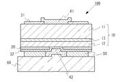
図1に、本実施形態に係る面発光レーザ素子の半導体積層方向における断面図を示す。本実施形態に係る面発光レーザ素子100は、第1半導体層11及び第2半導体層12を有する半導体部10と、半導体部10の第1半導体層11側に設けられた第1反射器41と、半導体部10の第2半導体層12側に設けられた第2反射器42と、を有する。特に、第2半導体層12と第2反射器42との間に設けられ第2半導体層12と接続された第2電極32と、第2反射器42の周囲に設けられ第2電極32と接続された接続電極50と、第2半導体層12と接続電極50との間に設けられ半導体部10からの光を反射可能な電流狭窄部20と、を備える。
<
FIG. 1 is a cross-sectional view of the surface emitting laser element according to this embodiment in the semiconductor stacking direction. The surface
第2半導体層12と接続電極50との間に半導体部10からの光を反射可能な電流狭窄部20を設けることで、接続電極50における光の吸収を抑制することができる。つまり、光反射が可能な電流狭窄部20を設けることで、接続電極50における光の損失を抑制することができる。これにより、閾値電流の低下や光出力の向上が期待できる。
By providing the
以下、本実施の形態の面発光レーザ素子の主な構成要素について説明する
(半導体部10)
半導体部10は、少なくとも第1半導体層11及び第2半導体層12を有していれば良く、その構造は特に限定されない。第1半導体層11は第1電極31を接続するための部材であり、第2半導体層12と異なる極性を有している。同様に、第2半導体層12は第2電極32を接続するための部材であり、第1半導体層11と異なる極性を有している。本実施形態では、第1半導体層11をn型、第2半導体層12をp型としており、両者の間に活性層13を備えたものを半導体部としている。活性層13の構造は限定されず、多重量子井戸構造や単一量子井戸構造など公知のものを採用することができる。半導体部10を構成する各層の材料は限定されないが、本実施形態では、一般式がInxAlyGa1−x−yN(0≦x≦1、0≦y≦1、0≦x+y≦1)で示される窒化物半導体を用いている。
Hereinafter, main components of the surface emitting laser element of the present embodiment will be described (semiconductor part 10).
The
(電流狭窄部20)
電流狭窄部20は、所望の領域(電流狭窄領域)に電流を狭窄するために設けられ、半導体部10からの光を反射することを目的として設けられる。電流狭窄部20の構成は限定されないが、本実施形態では、電流狭窄部20を誘電体多層膜からなるDBRから構成している。誘電体多層膜を構成する各層としては、SiO2、TiO2、Nb2O5、ZrO2、Ta2O5、HfO2、AlN、SiN、Al2O3、SiC、MgO等が例示される。これらの誘電体のうち、屈折率が異なる2種以上の材料層を所定の膜厚で交互に積層することにより半導体部10からの光を反射可能な誘電体多層膜からなる電流狭窄部20を得ることができる。例えば、SiO2/Nb2O5、SiO2/ZrO2、SiO2/AlN等の多層膜が好ましい。電流狭窄部20の膜厚は、0.03μm以上7.0μm未満、好ましくは0.04μm以上5.0μm未満、より好ましくは0.05μm以上3.0μm未満とすることができる。用いる材料によって決まる電流狭窄部全体の熱伝導率と反射率から適宜調整することが好ましい。
(Current constriction part 20)
The
電流狭窄部20は、半導体部10及び/又は第2電極31よりも屈折率が小さい材料であることが適している。このような屈折率を有することにより、横方向の光の閉じ込めを確実に行うことができる。
The
電流狭窄部20は、電流狭窄領域における定在波の位相と合うように調整されていることが好ましい。電流狭窄部20において、光の損失を効果的に低減させることができるからである。また、電流狭窄部20上の第2反射器42が形成されている領域と接続電極50が形成されている領域で層構造が異なっていても良い。光の損失をより低減させることができる。
The
(第1電極31)
本実施形態では、第1電極31はn電極として形成されている。n電極としての第1電極31は、Pd、Pt、Ni、Au、Ti、W、Cu、Ag、Zn、Sn、In、Al、Ir、Rh、V、ITO等のいずれかを含む構成とすることができる。
(First electrode 31)
In the present embodiment, the
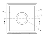
図2に、面発光レーザ素子100を第1反射器41側からみた平面図を示す。第1電極31は第1半導体層11が露出した開口部(図2の破線部分)を有しており、当該開口部が露出した領域で第1半導体層11と第1反射器41が接して設けられている。また、第1電極31の外縁は第1半導体層11の外縁近傍まで配置されている。
FIG. 2 is a plan view of the surface emitting
(第2電極32)
本実施形態では、第2電極32はp電極として形成されている。p電極としての第2電極32は、ZnO、In2O3、SnO2、ATO、ITO、MgO、Ni/Au、より好ましくはITOを用いることができる。その膜厚は特に限定されないが、5〜100nm程度とすることができる。なお、本実施の形態では活性層13からの光が第2電極32を透過して第2反射器42で反射されることを要するため、第2電極32はその光に対して実質的に透明である。
(Second electrode 32)
In the present embodiment, the
第2電極32は、電流狭窄部20の開口部内において第2半導体層12と直接接続されており、そこから更に電流狭窄部20と接続電極50の間において延在するように形成されている。
The
(接続電極50)
接続電極50は、第2電極32と電気的に接続される部材であり、第2反射器42を取り囲むようにその近傍に形成されている。換言すると、接続電極50は開口部を有しており、当該開口部内に第2反射器42が配されている。
(Connection electrode 50)
The
接続電極50には、高い電気伝導率及び熱伝導率が求められるので、その材料及び膜厚の関係から、第2電極32よりも半導体部10からの光に対して透光性が低く、半導体部10からの光を吸収しやすい(例えば非透光性)。接続電極50は、例えば、Ni、Au、Ag、Cu、Pt、Al、Pd、Rh、Ti、Mo、Cr又はWの少なくともいずれか一種を含む材料から構成することができる。より具体的には、Ti−Rh−Au、Cr−Pt−Au、Ni−Au、Ni−Au−Pt、Pd−Pt、Ni−Pt等が挙げられる。
Since the
第2反射器42が誘電体多層膜から構成される場合、一般に誘電体は半導体よりも熱伝導率が低いので、半導体部10からの放熱の問題が顕著となる。つまり、半導体部10では電流が流れる領域は電流狭窄領域に制限されているので電流狭窄領域が主な発熱源となるが、熱伝導率の低い誘電体多層膜からなる第2反射器42が電流狭窄領域と支持基板60との間に介在する場合、放熱経路が分断されて放熱性が損なわれてしまうという問題がある。一方、放熱性を向上させるには、熱伝導率に優れた接続電極50を電流狭窄領域に近付ければよいが、接続電極50を電流狭窄領域に近づけすぎると、今度は接続電極50による光の吸収が問題となってしまう。そこで、接続電極50と第2半導体層12との間に、電流を狭窄するだけでなく光を反射する機能を有する電流狭窄部20を介在させることにより、放熱性を向上させつつ光損失を軽減させた面発光レーザ素子とすることができる。
When the
電流狭窄部20の開口部の周縁は、接続電極50の開口部の周縁と実質的に一致しているか、好ましくは図1に示すように、接続電極50の開口部の周縁の内側に位置する(つまり、電流狭窄部20の開口部は接続電極50の開口部よりも小さい)ことが好ましい。電流狭窄部20で光が反射されることにより、接続電極50での光の吸収がより軽減できるからである。
The peripheral edge of the opening portion of the
図1では、接続電極50は、第2反射器42の周囲のみに設けられており、第2反射器42と支持基板60との間には設けられていない。ただ、必要に応じて、第2反射器42と支持基板60との間にも接続電極50を介在させてもよいことは言うまでもない。
In FIG. 1, the
(第1反射器41、第2反射器42)
第1反射器41及び第2反射器42は、半導体多層膜や誘電体多層膜から形成される。第1反射器41及び第2反射器42が誘電体多層膜からなる場合、誘電体多層膜を構成する各層としては、SiO2、TiO2、Nb2O5、ZrO2、Ta2O5、HfO2、AlN、SiN、Al2O3、SiC、MgO等が例示される。これらの誘電体のうち、屈折率が異なる2種以上の材料層を所定の膜厚で交互に積層することにより誘電体多層膜からなる第1反射器41及び第2反射器42を得ることができる。例えば、SiO2/Nb2O5、SiO2/ZrO2、SiO2/AlN等の多層膜が好ましい。第1反射器41、第2反射器42の膜厚としては、0.3μm以上7.0μm未満、好ましくは0.4μm以上6.0μm未満、より好ましくは0.5μm以上5.0μm未満とすることができる。用いる材料によって決まる第1反射器41及び第2反射器42全体の熱伝導率と反射率から適宜調整することが好ましい。
(
The
(支持基板60)
支持基板60は、接続電極50と接続される部材である。支持基板60としては種々のものを採用できるが、好ましくはSi、GaN、AlN、より好ましくはSiを用いることができる。
(Supporting substrate 60)
The
支持基板60は単層である必要はなく、多層であっても良い。さらに、本実施の形態では導電性の支持基板を用いているが、支持基板10は必ずしも導電性を備えている必要はなく、絶縁性であってもよい。支持基板10を絶縁性とする場合は、例えば支持基板に導電性のスルーホールを設け、スルーホールを介してコンタクト電極と通電させることもできる。
The
電流狭窄領域近傍において、第2反射器42側における支持基板60にAl等の高反射率部材を含有させることもできる。これにより、電流狭窄領域近傍における反射率をより向上させることができる。
In the vicinity of the current confinement region, the
<実施形態2>
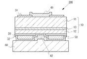
図3に、本実施形態に係る面発光レーザ素子200の断面図を示す。面発光レーザ素子200は、第2電極32と接続電極50が異なる以外は、実施形態1と実質的に同一である。
<Embodiment 2>
FIG. 3 is a cross-sectional view of the surface emitting
つまり、面発光レーザ素子200では、接続電極50は第2電極32を介在せずに電流狭窄部20と直接接しており、支持基板60は接続電極50を介在せずに第2電極32と直接接している。このような構成であっても実施形態1と同様の作用効果が期待できる。
That is, in the surface emitting
<実施形態3>
図4に、本実施形態に係る面発光レーザ素子300の断面図を示す。面発光レーザ素子300は、半導体部10において電流狭窄領域の周囲が電流狭窄領域に比較して薄くなったおり、それにより凸部が形成されていること、凸部の第2反射器42が設けられている側だけでなく側面(第1反射器41と第2反射器42とを結ぶ直線に平行な面)にも光反射が可能な電流狭窄部20が設けられていること、が実施形態2の面発光レーザ素子200と主に異なっている。
<Embodiment 3>
FIG. 4 is a sectional view of the surface emitting
面発光レーザ素子300では、活性層13を含む凸部の側面に光を反射するための電流狭窄部20が形成されている。これにより、横方向における強い光閉じ込めが期待できる。
In the surface emitting
実施形態1〜3では、第1電極31と第2電極32とが半導体部10を介して互いに反対となるように構成しているが、本願発明に係る面発光レーザ素子はこれに限定されない。例えば、半導体部10の一部を第2半導体層12側から第1半導体層11が露出するように除去し、当該除去部分に第1電極31を形成してもよい。
In the first to third embodiments, the
10…半導体部
11…第1半導体層
12…第2半導体層
13…活性層
20…電流狭窄部
31…第1電極
32…第2電極
41…第1反射器
42…第2反射器
50…接続電極
60…支持基板
DESCRIPTION OF
Claims (3)
前記第2半導体層と前記第2反射器との間に設けられ、前記第2半導体層と接続された第2電極と、
前記第2反射器の周囲に設けられ、前記第2電極と接続された接続電極と、
前記第2半導体層と前記接続電極との間に設けられ、前記半導体部からの光を反射可能な電流狭窄部と、を備えることを特徴とする面発光レーザ素子。 A semiconductor part having a first semiconductor layer and a second semiconductor layer, a first reflector provided on the first semiconductor layer side of the semiconductor part, and a second reflection provided on the second semiconductor layer side of the semiconductor part A surface-emitting laser element having:
A second electrode provided between the second semiconductor layer and the second reflector and connected to the second semiconductor layer;
A connection electrode provided around the second reflector and connected to the second electrode;
A surface emitting laser device comprising: a current confinement portion provided between the second semiconductor layer and the connection electrode and capable of reflecting light from the semiconductor portion.
前記接続電極は、開口部を有し、
前記電流狭窄部の開口部は、前記接続電極の開口部の内側に配置されていることを特徴とする請求項1又は2に記載の面発光レーザ素子。 The current confinement portion has an opening,
The connection electrode has an opening,
3. The surface emitting laser element according to claim 1, wherein the opening portion of the current confinement portion is disposed inside the opening portion of the connection electrode.
Priority Applications (2)
| Application Number | Priority Date | Filing Date | Title |
|---|---|---|---|
| JP2011050939A JP5633435B2 (en) | 2011-03-09 | 2011-03-09 | Surface emitting laser element |
| US13/413,375 US8855157B2 (en) | 2011-03-09 | 2012-03-06 | Surface emitting laser element |
Applications Claiming Priority (1)
| Application Number | Priority Date | Filing Date | Title |
|---|---|---|---|
| JP2011050939A JP5633435B2 (en) | 2011-03-09 | 2011-03-09 | Surface emitting laser element |
Publications (2)
| Publication Number | Publication Date |
|---|---|
| JP2012190867A true JP2012190867A (en) | 2012-10-04 |
| JP5633435B2 JP5633435B2 (en) | 2014-12-03 |
Family
ID=46795550
Family Applications (1)
| Application Number | Title | Priority Date | Filing Date |
|---|---|---|---|
| JP2011050939A Active JP5633435B2 (en) | 2011-03-09 | 2011-03-09 | Surface emitting laser element |
Country Status (2)
| Country | Link |
|---|---|
| US (1) | US8855157B2 (en) |
| JP (1) | JP5633435B2 (en) |
Cited By (1)
| Publication number | Priority date | Publication date | Assignee | Title |
|---|---|---|---|---|
| JPWO2014065332A1 (en) * | 2012-10-26 | 2016-09-08 | 大学共同利用機関法人情報・システム研究機構 | Light generating device and light generating method |
Families Citing this family (4)
| Publication number | Priority date | Publication date | Assignee | Title |
|---|---|---|---|---|
| KR102420016B1 (en) | 2015-08-28 | 2022-07-12 | 삼성전자주식회사 | Optical modulator having reflection layers |
| CN111869022B (en) * | 2018-03-19 | 2024-03-15 | 株式会社理光 | Surface-emitting laser array, detection device and laser device |
| JP7166871B2 (en) * | 2018-10-18 | 2022-11-08 | スタンレー電気株式会社 | Vertical cavity light emitting device |
| CN110277732A (en) * | 2019-07-16 | 2019-09-24 | 河北工业大学 | VCSEL device and preparation method thereof with high dielectric constant limiting holes |
Citations (3)
| Publication number | Priority date | Publication date | Assignee | Title |
|---|---|---|---|---|
| JP2010123921A (en) * | 2008-10-22 | 2010-06-03 | Nichia Corp | Method for manufacturing nitride semiconductor light-emitting element and nitride semiconductor light-emitting element |
| JP2011029607A (en) * | 2009-06-30 | 2011-02-10 | Nichia Corp | Vertical resonator type surface-emitting laser |
| JP2011175993A (en) * | 2010-02-23 | 2011-09-08 | Nichia Corp | Nitride semiconductor laser element |
Family Cites Families (18)
| Publication number | Priority date | Publication date | Assignee | Title |
|---|---|---|---|---|
| JPS63318195A (en) * | 1987-06-19 | 1988-12-27 | Agency Of Ind Science & Technol | Transverse buried type surface emitting laser |
| US4943970A (en) * | 1988-10-24 | 1990-07-24 | General Dynamics Corporation, Electronics Division | Surface emitting laser |
| US5070509A (en) * | 1990-08-09 | 1991-12-03 | Eastman Kodak Company | Surface emitting, low threshold (SELTH) laser diode |
| US5331658A (en) * | 1992-08-26 | 1994-07-19 | Motorola, Inc. | Vertical cavity surface emitting laser and sensor |
| KR100243656B1 (en) * | 1996-12-05 | 2000-02-01 | 정선종 | A vertical-cavity surface-emitting LASER with hydrogenation treatment and method for fabricating the same |
| US6760357B1 (en) * | 1998-04-14 | 2004-07-06 | Bandwidth9 | Vertical cavity apparatus with tunnel junction |
| EP1399994B1 (en) * | 2001-06-20 | 2005-07-27 | Infineon Technologies AG | Photon emitter and data transmission device |
| JP3860494B2 (en) * | 2002-03-13 | 2006-12-20 | 富士通株式会社 | Surface emitting laser and manufacturing method thereof |
| JP4590820B2 (en) * | 2002-12-16 | 2010-12-01 | 富士ゼロックス株式会社 | Surface emitting semiconductor laser and manufacturing method thereof |
| US7564887B2 (en) * | 2004-06-30 | 2009-07-21 | Finisar Corporation | Long wavelength vertical cavity surface emitting lasers |
| JP5017804B2 (en) * | 2005-06-15 | 2012-09-05 | 富士ゼロックス株式会社 | Tunnel junction type surface emitting semiconductor laser device and manufacturing method thereof |
| JP2007142375A (en) * | 2005-10-20 | 2007-06-07 | Furukawa Electric Co Ltd:The | Surface emitting laser element, and method of manufacturing same |
| JP2007234824A (en) * | 2006-02-28 | 2007-09-13 | Canon Inc | Vertical resonator type surface-emitting laser |
| US7573074B2 (en) * | 2006-05-19 | 2009-08-11 | Bridgelux, Inc. | LED electrode |
| JP5027010B2 (en) * | 2007-03-01 | 2012-09-19 | 古河電気工業株式会社 | Surface emitting laser element |
| JP4878322B2 (en) * | 2007-03-29 | 2012-02-15 | 古河電気工業株式会社 | Surface emitting laser element and method for manufacturing surface emitting laser element |
| JP2009246291A (en) * | 2008-03-31 | 2009-10-22 | Furukawa Electric Co Ltd:The | Surface emitting laser element array |
| JP4902682B2 (en) * | 2009-03-27 | 2012-03-21 | キヤノン株式会社 | Nitride semiconductor laser |
-
2011
- 2011-03-09 JP JP2011050939A patent/JP5633435B2/en active Active
-
2012
- 2012-03-06 US US13/413,375 patent/US8855157B2/en active Active
Patent Citations (3)
| Publication number | Priority date | Publication date | Assignee | Title |
|---|---|---|---|---|
| JP2010123921A (en) * | 2008-10-22 | 2010-06-03 | Nichia Corp | Method for manufacturing nitride semiconductor light-emitting element and nitride semiconductor light-emitting element |
| JP2011029607A (en) * | 2009-06-30 | 2011-02-10 | Nichia Corp | Vertical resonator type surface-emitting laser |
| JP2011175993A (en) * | 2010-02-23 | 2011-09-08 | Nichia Corp | Nitride semiconductor laser element |
Cited By (1)
| Publication number | Priority date | Publication date | Assignee | Title |
|---|---|---|---|---|
| JPWO2014065332A1 (en) * | 2012-10-26 | 2016-09-08 | 大学共同利用機関法人情報・システム研究機構 | Light generating device and light generating method |
Also Published As
| Publication number | Publication date |
|---|---|
| US20120230360A1 (en) | 2012-09-13 |
| JP5633435B2 (en) | 2014-12-03 |
| US8855157B2 (en) | 2014-10-07 |
Similar Documents
| Publication | Publication Date | Title |
|---|---|---|
| JP5633477B2 (en) | Light emitting element | |
| JP5929714B2 (en) | Semiconductor light emitting device | |
| KR101226706B1 (en) | Semiconductor light emimitting device | |
| JP5541261B2 (en) | Group III nitride semiconductor light emitting device | |
| JP2018121059A (en) | Light-emitting element | |
| JP5633435B2 (en) | Surface emitting laser element | |
| JP2011138820A (en) | Light-emitting element | |
| JP2007258276A (en) | Semiconductor light emitting device | |
| JP6664688B2 (en) | Vertical cavity light emitting device | |
| US20080217634A1 (en) | Vertical light-emitting diode structure with omni-directional reflector | |
| JP6149878B2 (en) | Light emitting element | |
| JP5724316B2 (en) | Nitride semiconductor laser device | |
| JP2017117904A (en) | Light-emitting element and method for manufacturing the same | |
| JP2017157650A (en) | Semiconductor light emitting element | |
| KR101165253B1 (en) | Light emitting diode | |
| JP5378131B2 (en) | Nitride semiconductor light emitting diode device | |
| US10396248B2 (en) | Semiconductor light emitting diode | |
| JP5857707B2 (en) | Surface emitting laser element | |
| JP6651843B2 (en) | Light emitting element | |
| JP5573222B2 (en) | Nitride semiconductor laser device | |
| JP7227469B2 (en) | Vertical cavity surface emitting laser device | |
| JP5974808B2 (en) | Semiconductor light emitting device | |
| JP5745250B2 (en) | Light emitting device | |
| JP2012142339A (en) | Semiconductor device | |
| KR101544128B1 (en) | Semiconductor light emitting device |
Legal Events
| Date | Code | Title | Description |
|---|---|---|---|
| A621 | Written request for application examination |
Free format text: JAPANESE INTERMEDIATE CODE: A621 Effective date: 20131010 |
|
| A977 | Report on retrieval |
Free format text: JAPANESE INTERMEDIATE CODE: A971007 Effective date: 20140319 |
|
| A131 | Notification of reasons for refusal |
Free format text: JAPANESE INTERMEDIATE CODE: A131 Effective date: 20140408 |
|
| A521 | Request for written amendment filed |
Free format text: JAPANESE INTERMEDIATE CODE: A523 Effective date: 20140425 |
|
| TRDD | Decision of grant or rejection written | ||
| A01 | Written decision to grant a patent or to grant a registration (utility model) |
Free format text: JAPANESE INTERMEDIATE CODE: A01 Effective date: 20140916 |
|
| A61 | First payment of annual fees (during grant procedure) |
Free format text: JAPANESE INTERMEDIATE CODE: A61 Effective date: 20140929 |
|
| R150 | Certificate of patent or registration of utility model |
Ref document number: 5633435 Country of ref document: JP Free format text: JAPANESE INTERMEDIATE CODE: R150 |
|
| R250 | Receipt of annual fees |
Free format text: JAPANESE INTERMEDIATE CODE: R250 |
|
| R250 | Receipt of annual fees |
Free format text: JAPANESE INTERMEDIATE CODE: R250 |
|
| R250 | Receipt of annual fees |
Free format text: JAPANESE INTERMEDIATE CODE: R250 |
|
| R250 | Receipt of annual fees |
Free format text: JAPANESE INTERMEDIATE CODE: R250 |
|
| R250 | Receipt of annual fees |
Free format text: JAPANESE INTERMEDIATE CODE: R250 |
|
| R250 | Receipt of annual fees |
Free format text: JAPANESE INTERMEDIATE CODE: R250 |