JP2012185032A - Displacement sensor - Google Patents
Displacement sensor Download PDFInfo
- Publication number
- JP2012185032A JP2012185032A JP2011048173A JP2011048173A JP2012185032A JP 2012185032 A JP2012185032 A JP 2012185032A JP 2011048173 A JP2011048173 A JP 2011048173A JP 2011048173 A JP2011048173 A JP 2011048173A JP 2012185032 A JP2012185032 A JP 2012185032A
- Authority
- JP
- Japan
- Prior art keywords
- sensor
- coil
- sensor coil
- displacement sensor
- current
- Prior art date
- Legal status (The legal status is an assumption and is not a legal conclusion. Google has not performed a legal analysis and makes no representation as to the accuracy of the status listed.)
- Granted
Links
Images


Abstract
Description
本発明は、変位センサに関する。
より詳細には、高感度且つ安定した検出性能を実現する変位センサに関する。
The present invention relates to a displacement sensor.
More specifically, the present invention relates to a displacement sensor that realizes high sensitivity and stable detection performance.
出願人は、抵抗スライダと違い、電気機械的接触部品を伴わずに、直線変位量をリニアなアナログ電圧で出力できる、アクティブ型変位センサを製造販売している。以下、このアクティブ型変位センサの動作原理について説明する。 Unlike the resistance slider, the applicant manufactures and sells an active displacement sensor that can output a linear displacement amount with a linear analog voltage without an electromechanical contact part. Hereinafter, the operation principle of the active displacement sensor will be described.
特許文献1は、出願人による変位センサの先行技術文献である。特許文献1に開示されている技術内容は、コイルのインダクタンスの変化を利用して変位を検出するための技術である。
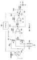
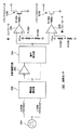
図16は特許文献1に開示されている、変位センサの検出回路の回路図である。
コイルA及びコイルBには、トランス1602を介して矩形波発生器の矩形波が印加される。
コイルAに流れる電流は、ダイオードD1603を通じてコンデンサC1604に流れ、コンデンサC1604には電荷が蓄積される。コイルAとコンデンサC1604との間のダイオードD1603は、コイルからコンデンサに流れる電流を片方向に制限する。ダイオードD1603に電流が流れない期間では、コンデンサC1604に蓄積された電荷は、コンデンサC1604に並列接続されている抵抗R1605によって放電される。したがって、コンデンサC1604の両端(端子1610Bと端子1610Cとの間)には鋸歯状波が得られる。
Patent document 1 is a prior art document of the displacement sensor by the applicant. The technical content disclosed in Patent Document 1 is a technique for detecting a displacement using a change in inductance of a coil.
FIG. 16 is a circuit diagram of a detection circuit of a displacement sensor disclosed in Patent Document 1.
The rectangular wave of the rectangular wave generator is applied to the coil A and the coil B through the
The current flowing through the coil A flows to the capacitor C1604 through the diode D1603, and electric charge is accumulated in the capacitor C1604. A diode D1603 between the coil A and the capacitor C1604 limits the current flowing from the coil to the capacitor in one direction. During a period when no current flows through the diode D1603, the electric charge accumulated in the capacitor C1604 is discharged by the resistor R1605 connected in parallel to the capacitor C1604. Accordingly, a sawtooth wave is obtained at both ends of the capacitor C1604 (between the terminals 1610B and 1610C).
コイルBに流れる電流は、ダイオードD1606を通じてコンデンサC1607に流れ、コンデンサC1607には電荷が蓄積される。コイルBとコンデンサC1607との間のダイオードD1606は、コイルからコンデンサに流れる電流を片方向に制限する。ダイオードD1606に電流が流れない期間では、コンデンサC1607に蓄積された電荷は、コンデンサC1607に並列接続されている抵抗R1608によって放電される。したがって、コンデンサC1607の両端(端子1610Aと端子1610Cとの間)には、コンデンサC1604の両端には鋸歯状波が得られる。
端子1610Aと端子1610Bから得られる信号を図示しない差動増幅回路で差動増幅すると、直流電圧が得られる。この直流電圧は、コイルA及びコイルBのインダクタンスに応じて変化する。
The current flowing through the coil B flows to the capacitor C1607 through the diode D1606, and electric charge is accumulated in the capacitor C1607. A diode D1606 between the coil B and the capacitor C1607 limits the current flowing from the coil to the capacitor in one direction. In a period in which no current flows through the diode D1606, the charge accumulated in the capacitor C1607 is discharged by the resistor R1608 connected in parallel to the capacitor C1607. Therefore, sawtooth waves are obtained at both ends of the capacitor C1607 (between the
When signals obtained from the
コイルA及びコイルBは、それぞれ合成樹脂の筒(プローブ)に収納され、変位センサの検出コイルとして用いられる。このプローブに真鍮製の筒(スリーブ)が被さり、プローブを移動すると、変位センサはその位置に応じた直流電圧を出力する。
コイルA及びコイルBのそれぞれに同じ検出回路が接続され、同相の鋸歯状波が検出され、筒が被さった方の検出出力が小さくなる。両方の検出出力信号を差動増幅器で差動増幅すると、検出コイルのインダクタンスの変化に基づいて、出力電圧が変化する。
The coil A and the coil B are each housed in a synthetic resin tube (probe) and used as a detection coil of a displacement sensor. When this probe is covered with a brass tube (sleeve) and the probe is moved, the displacement sensor outputs a DC voltage corresponding to the position.
The same detection circuit is connected to each of the coil A and the coil B, the in-phase sawtooth wave is detected, and the detection output on the side covered with the cylinder becomes small. When both detection output signals are differentially amplified by the differential amplifier, the output voltage changes based on the change in the inductance of the detection coil.
例えば、自動車や自動二輪車のサスペンションに変位センサを装着して、サスペンションの変位を計測する場合、サスペンションには強い力が加わるので、変位センサを構成する合成樹脂のプローブは機械衝撃に耐えられず、破損することがあった。
そこで、出願人および発明者は、プローブの機械強度を上げるため、プローブの外殻を金属製に代える検討を始めた。
しかし、変位センサがコイルのインダクタンスの変化を検出する仕組みであるが故に、プローブの外殻を金属製にすると、外殻に渦電流に起因する損失が発生し、位置検出感度が著しく低下する。
更に、図16に開示する、従来技術の変位センサの回路構成では、検出感度を上昇させるためにコイルに流す電流を大きくしても、渦電流損失ばかり大きくなり、感度の向上に殆ど寄与しないことが判った。
For example, when a displacement sensor is mounted on a suspension of an automobile or a motorcycle and the displacement of the suspension is measured, since a strong force is applied to the suspension, the synthetic resin probe constituting the displacement sensor cannot withstand mechanical shock, It was sometimes damaged.
Therefore, the applicant and the inventor have started to study to replace the outer shell of the probe with metal in order to increase the mechanical strength of the probe.
However, since the displacement sensor is a mechanism for detecting a change in the inductance of the coil, if the outer shell of the probe is made of metal, a loss due to eddy current occurs in the outer shell, and the position detection sensitivity is significantly reduced.
Further, in the circuit configuration of the conventional displacement sensor disclosed in FIG. 16, even if the current flowing through the coil is increased in order to increase the detection sensitivity, only the eddy current loss is increased, and this hardly contributes to the improvement of the sensitivity. I understood.
また、図16に開示する変位センサは、コンパレータで二値化すると、金属物の存在を検出する近接センサとしても利用できる。しかし、これも機械強度を確保するために金属製の筐体に収納すると、前述の変位センサと同様の問題を生じることとなる。 The displacement sensor disclosed in FIG. 16 can also be used as a proximity sensor that detects the presence of a metal object when binarized by a comparator. However, if this is housed in a metal housing in order to ensure mechanical strength, the same problem as that of the aforementioned displacement sensor will occur.
本発明はかかる課題を解決し、検出コイルを金属製の外殻で覆っても、渦電流損失を小さく抑え、必要十分な位置検出感度を得ることができる変位センサを提供することを目的とする。 SUMMARY OF THE INVENTION An object of the present invention is to solve such problems and to provide a displacement sensor that can suppress eddy current loss and obtain necessary and sufficient position detection sensitivity even when a detection coil is covered with a metal outer shell. .
更に、本発明はかかる課題を解決し、検出コイルを金属製の外殻で覆っても、渦電流損失を小さく抑え、必要十分な位置検出感度を得ることができる近接センサを提供することを目的とする。 It is another object of the present invention to provide a proximity sensor that solves such problems and can suppress eddy current loss and obtain necessary and sufficient position detection sensitivity even when the detection coil is covered with a metal outer shell. And
上記課題を解決するために、本発明の変位センサは、第一センサコイルと、第二センサコイルと、第一センサコイル及び/又は第二センサコイルのインダクタンスを変化させる金属製のスリーブと、第一センサコイル及び第二センサコイルに矩形波電圧を供給する矩形波電圧源と、第一センサコイルに流れる第一の電流と、第二センサコイルに流れる第二の電流との差を検出して電圧信号を出力する電流差検出部と、電流差検出部から得られる電流差信号の電位を反転する反転増幅回路と、電流差信号と反転増幅回路の出力信号を基に第一センサコイル及び第二センサコイルの相対的インダクタンスの差に応じて変化する信号を出力する電圧検出部とを具備する。 In order to solve the above problems, a displacement sensor of the present invention includes a first sensor coil, a second sensor coil, a metal sleeve that changes the inductance of the first sensor coil and / or the second sensor coil, Detecting a difference between a rectangular wave voltage source that supplies a rectangular wave voltage to one sensor coil and a second sensor coil, a first current flowing through the first sensor coil, and a second current flowing through the second sensor coil; A current difference detector that outputs a voltage signal; an inverting amplifier that inverts the potential of the current difference signal obtained from the current difference detector; and the first sensor coil and the second sensor coil based on the output signal of the current difference signal and the inverting amplifier. A voltage detection unit that outputs a signal that changes in accordance with a difference in relative inductance between the two sensor coils.
また、上記課題を解決するために、本発明の近接センサは、非磁性体金属及び/又は磁性体が近接するとインダクタンスが変化する検出コイルと、検出コイルと電気的特性が等しい参照コイルと、検出コイル及び参照コイルに矩形波電圧を供給する矩形波電圧源と、検出コイルに流れる第一の電流と、参照コイルに流れる第二の電流との差を検出して電圧信号を出力する電流差検出部と、電流差検出部から得られる電流差信号の電位を反転する反転増幅回路と、電流差信号と反転増幅回路の出力信号を基に検出コイル及び参照コイルの相対的インダクタンスの差に応じて変化する信号を出力する電圧検出部と、電圧検出部が出力する信号を二値化するコンパレータとを具備する。 In order to solve the above problems, a proximity sensor according to the present invention includes a detection coil whose inductance changes when a non-magnetic metal and / or magnetic material approaches, a reference coil having the same electrical characteristics as the detection coil, and a detection coil Current difference detection that outputs a voltage signal by detecting a difference between a rectangular wave voltage source that supplies a rectangular wave voltage to the coil and the reference coil, a first current flowing through the detection coil, and a second current flowing through the reference coil And an inverting amplification circuit that inverts the potential of the current difference signal obtained from the current difference detection unit, and a difference in relative inductance between the detection coil and the reference coil based on the output signal of the current difference signal and the inverting amplification circuit. A voltage detection unit that outputs a changing signal and a comparator that binarizes the signal output from the voltage detection unit.
二つのコイルに矩形波電圧を印加して、各々のコイルに流れる電流を独立して検出してから差動回路等で差を演算するのではなく、直接電流の差の値を検出することにより、S/N比が良好であり高感度な変位センサを実現できる。
また、各々のコイルは同じ磁気特性と電気特性を備えるため、温度変化でこれらの特性が変化したとしても夫々同じように変化するので、温度変化に起因するばらつきが生じ難い。
By detecting the value of the current difference directly, instead of calculating the difference with a differential circuit etc. after applying a rectangular wave voltage to the two coils and independently detecting the current flowing through each coil Thus, a highly sensitive displacement sensor with a good S / N ratio can be realized.
In addition, since each coil has the same magnetic characteristics and electrical characteristics, even if these characteristics change due to a temperature change, they change in the same way, so that variations due to the temperature change hardly occur.
本発明により、検出コイルを金属製の外殻で覆っても、渦電流損失を小さく抑え、必要十分な位置検出感度を得ることができる変位センサを提供できる。 According to the present invention, it is possible to provide a displacement sensor that can suppress eddy current loss and obtain necessary and sufficient position detection sensitivity even if the detection coil is covered with a metal outer shell.
また、本発明により、検出コイルを金属製の外殻で覆っても、渦電流損失を小さく抑え、必要十分な位置検出感度を得ることができる近接センサを提供できる。 Further, according to the present invention, it is possible to provide a proximity sensor that can suppress eddy current loss and obtain necessary and sufficient position detection sensitivity even when the detection coil is covered with a metal outer shell.
本実施形態では、変位センサと、近接センサを開示する。
第一の実施形態及び第二の実施形態にて開示する変位センサは、二つのコイルを用いて、基準点から正負方向に移動体が変位した際の変位量を正負両極性のアナログ信号として出力する。
第三の実施形態、第四の実施形態及び第五の実施形態にて開示する近接センサは、二つのコイルを用いて、変位センサと同じ動作原理にて非磁性体金属及び/又は磁性体がセンサコイルに近接したことをデジタルの論理信号として出力する。
In this embodiment, a displacement sensor and a proximity sensor are disclosed.
The displacement sensor disclosed in the first embodiment and the second embodiment uses two coils and outputs the displacement amount when the moving body is displaced in the positive and negative directions from the reference point as an analog signal of both positive and negative polarities. To do.
The proximity sensor disclosed in the third embodiment, the fourth embodiment, and the fifth embodiment uses two coils, and the non-magnetic metal and / or magnetic body is made of the same operating principle as the displacement sensor. The proximity of the sensor coil is output as a digital logic signal.
[第一の実施形態・変位センサの外観]
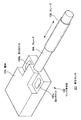
図1は、本発明の第一の実施形態に係る変位センサの外観斜視図である。
変位センサ101は、センサ本体部102とスリーブ103の組み合わせよりなる。
センサ本体部102は、検出回路を内蔵する筐体105の一端に、円筒形状のプローブ104が取り付けられている。
筐体105には、センサ本体部102を任意の物品に固定するための取り付け穴105a及び105bが設けられている。
プローブ104には後述する検出コイルである第一センサコイルL201及び第二センサコイルL202が内蔵されている。このプローブ104に、真鍮製の筒であるスリーブ103が挿入される。
スリーブ103がプローブ104を左右に移動すると、センサ本体部102は、プローブ104に対するスリーブ103の位置に応じた、アナログの検出信号を出力する。
[Appearance of first embodiment / displacement sensor]
FIG. 1 is an external perspective view of a displacement sensor according to a first embodiment of the present invention.
The displacement sensor 101 is a combination of a sensor
In the sensor
The
The probe 104 includes a first sensor coil L201 and a second sensor coil L202 which are detection coils described later. A
When the
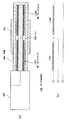
図2(a)及び(b)は、変位センサ101の一部断面図とセンサコイルの回路図である。
図2(a)は、変位センサ101を横から見た状態で、スリーブ103とプローブ104について断面形状を示す一部断面図である。
プローブ104の外殻104aは剛性を向上させるために、本出願人の従来製品の樹脂モールドではなく、非磁性体であるオーステナイト系のステンレスで形成され、検出コイルである第一センサコイルL201及び第二センサコイルL202を内蔵する。
2A and 2B are a partial cross-sectional view of the displacement sensor 101 and a circuit diagram of the sensor coil.
FIG. 2A is a partial cross-sectional view showing a cross-sectional shape of the
In order to improve rigidity, the outer shell 104a of the probe 104 is not made of the resin mold of the applicant's conventional product but is formed of austenitic stainless steel that is a nonmagnetic material, and the first sensor coil L201 and the first sensor coil L201 that are detection coils. A two-sensor coil L202 is incorporated.
周知のとおり、オーステナイト系のステンレスは剛性が高い非磁性体金属であり、更に抵抗率が高いので、プローブ104に用いる場合、抵抗率の低い金属と比べると渦電流を小さく抑えることができる。しかしながら、抵抗率が高いとはいえどもステンレスは導体であるので、コイルに交流電流を流した際に渦電流の発生は免れない。渦電流は熱エネルギーに変換され、結果としてコイルのインダクタンスの低下を招く。
なお、プローブ104の外殻104aの材質は、必ずしもステンレスに限られないが、一定の条件が求められる。前述のように、非磁性体金属であることと、抵抗率が高いことである。抵抗率は、スリーブ103の抵抗率より高いことが好ましい。本実施形態の場合はスリーブ103の材質である真鍮(黄銅)が5〜7×10⁻⁸nΩmであるのに対し、ステンレスは7.2×10⁻⁷nΩmなので、この条件を満たす。
As is well known, austenitic stainless steel is a non-magnetic metal having high rigidity and has a high resistivity. Therefore, when used for the probe 104, the eddy current can be suppressed to be smaller than that of a metal having a low resistivity. However, although stainless steel is a conductor even though the resistivity is high, generation of eddy current is inevitable when an alternating current is passed through the coil. Eddy currents are converted into thermal energy, resulting in a reduction in coil inductance.
The material of the outer shell 104a of the probe 104 is not necessarily limited to stainless steel, but certain conditions are required. As described above, it is a non-magnetic metal and has a high resistivity. The resistivity is preferably higher than the resistivity of the
第一センサコイルL201及び第二センサコイルL202は図2(a)に示すように、プローブ104の内部に長手方向に設けられている、円柱形状のフェライトのコア203に巻きつけられている。つまり、プローブ104は、コア203を中心として、コア203に第一センサコイルL201及び第二センサコイルL202が巻きつけられ、これら第一センサコイルL201及び第二センサコイルL202を外殻104aが被さることによって形成される。
スリーブ103の長さは、第一センサコイルL201及び第二センサコイルL202の長さと同一か、やや長い。
図2(b)はコイルの回路図である。第一センサコイルL201及び第二センサコイルL202は、一端が接続され、三つの端子が設けられている。
As shown in FIG. 2A, the first sensor coil L201 and the second sensor coil L202 are wound around a cylindrical ferrite core 203 provided in the probe 104 in the longitudinal direction. That is, in the probe 104, the first sensor coil L201 and the second sensor coil L202 are wound around the core 203 around the core 203, and the outer shell 104a covers the first sensor coil L201 and the second sensor coil L202. Formed by.
The length of the
FIG. 2B is a circuit diagram of the coil. One end of the first sensor coil L201 and the second sensor coil L202 is connected, and three terminals are provided.
[第一の実施形態・変位センサの概念]
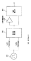
図3は、変位センサ101のブロック図である。図3のブロック図は、第一の実施形態に係る変位センサ101と、後述する第二の実施形態に係る変位センサの、上位概念を示す。
矩形波電圧源301は、第一センサコイルL201及び第二センサコイルL202に夫々矩形波の交流電圧を印加する。電流差検出部302は、第一センサコイルL201及び第二センサコイルL202に流れる電流の差を検出し、電流の差に応じた電圧信号を出力する。電流差検出部302は交流の検出信号を出力するので、これを直流にするため、反転増幅回路303と電圧検出部304を用いて、直流の変位検出信号を生成する。
[First Embodiment / Displacement Sensor Concept]
FIG. 3 is a block diagram of the displacement sensor 101. The block diagram of FIG. 3 shows a general concept of the displacement sensor 101 according to the first embodiment and the displacement sensor according to the second embodiment described later.
The rectangular
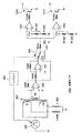
[第一の実施形態・変位センサの回路構成]
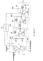
図4は、変位センサ101の回路図である。
第一矩形波電圧源401と第二矩形波電圧源402は、シーケンサ403の制御に基づいて、同じ電圧且つ相互に逆位相の矩形波電圧を生成する。
第一矩形波電圧源401の一端には第一センサコイルL201が接続され、第二矩形波電圧源402の一端には第二センサコイルL202が接続されている。第一矩形波電圧源401の他端と第二矩形波電圧源402の他端は接地されている。
第一センサコイルL201と第二センサコイルL202の接続中点には、オペアンプ404の反転入力端子が接続される。オペアンプ404の非反転入力端子は接地され、オペアンプ404の反転入力端子と出力端子との間には、帰還抵抗である抵抗R405が接続されている。オペアンプ404と抵抗R405は、周知の電流電圧変換回路を構成する。
[First Embodiment / Circuit Configuration of Displacement Sensor]
FIG. 4 is a circuit diagram of the displacement sensor 101.
The first rectangular
A first sensor coil L201 is connected to one end of the first rectangular
The inverting input terminal of the
オペアンプ404の出力端子は抵抗R406を介してオペアンプ407の反転入力端子に接続される。オペアンプ404の反転入力端子と出力端子との間には、帰還抵抗である抵抗R408が接続されている。抵抗R406と抵抗R408の抵抗値は等しい。したがって、オペアンプ404と抵抗R405及び抵抗R405は、増幅率が「−1」の、周知の反転増幅回路303を構成する。
The output terminal of the
オペアンプ404の出力端子とオペアンプ407の出力端子は、夫々アナログスイッチ409に接続される。アナログスイッチ409はシーケンサ403によって切り替え制御される。反転増幅回路303とアナログスイッチ409は、周知の同期整流回路を構成する。詳細は図5にて後述するが、アナログスイッチ409の出力端子には、三角波形状の脈流の信号が出力される。
アナログスイッチ409の出力端子には、抵抗R410が接続され、抵抗R410の他端にはコンデンサC411が接続される。コンデンサC411の他端は接地される。抵抗R405とコンデンサC411は周知の積分器を構成するので、脈流の信号から交流成分が除去され、出力端子から直流信号が出力される。
The output terminal of the
A resistor R410 is connected to the output terminal of the
[第一の実施形態・変位センサの動作]
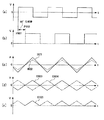
図5(a)、(b)、(c)、(d)、(e)及び(f)は、図4に示した変位センサ101の、各部の信号波形図である。
図5(a)は、第一矩形波電圧源401の電圧波形である。
図5(b)は、第二矩形波電圧源402の電圧波形である。
図5(c)は、シーケンサ403からアナログスイッチ409に与えられる制御信号の波形である。
図5(d)は、第一センサコイルL201及び第二センサコイルL202の電流波形である。
図5(e)は、オペアンプ404の出力端子及びオペアンプ404の出力端子の電圧波形である。
図5(f)は、アナログスイッチ409の出力信号波形である。
なお、図5(a)、(b)、(c)、(d)、(e)及び(f)は、横軸が同一の時間軸である。
[First Embodiment: Operation of Displacement Sensor]
5 (a), (b), (c), (d), (e), and (f) are signal waveform diagrams of each part of the displacement sensor 101 shown in FIG.
FIG. 5A shows a voltage waveform of the first rectangular
FIG. 5B shows a voltage waveform of the second rectangular
FIG. 5C shows a waveform of a control signal given from the
FIG. 5D shows current waveforms of the first sensor coil L201 and the second sensor coil L202.
FIG. 5E shows voltage waveforms at the output terminal of the
FIG. 5F shows the output signal waveform of the
5A, 5B, 5C, 5D, 5E, and 5F are time axes having the same horizontal axis.
コイルに矩形波の交流電圧を与えると(図5(a)及び(b))、電流波形は周知であるコイルの自己誘導特性によって三角波形状になる(図5(d))。
第一センサコイルL201と第二センサコイルL202の接続中点は、周知のオペアンプ404のイマジナルショートによって仮想的な接地状態になっている。
オペアンプ404は、第一センサコイルL201に流れる電流I421と、第二センサコイルL202に流れる電流I422の差(I421−I422)が抵抗R405に流れるように動作する。したがって、オペアンプ404の出力端子には電流差に比例した電圧(図5(e)のE423)が出力される。
When a rectangular wave AC voltage is applied to the coil (FIGS. 5A and 5B), the current waveform becomes a triangular wave shape due to the well-known self-induction characteristics of the coil (FIG. 5D).
The midpoint of connection between the first sensor coil L201 and the second sensor coil L202 is in a virtual ground state due to an imaginary short circuit of the well-known
The
図5(d)を見て判るように、第一センサコイルL201及び第二センサコイルL202の電流の差は、図5(e)の実線(電流差信号E423)で示す波形になる。図5(e)の実線に示す電流差信号E423の波形は交流なので、直流電圧信号に変換するには整流と積分が必要になる。そこで、図5(e)の電流差信号E423の波形のゼロクロスの時点で同期整流を行うように、アナログスイッチ409を制御する。このための制御信号が、第一矩形波電圧源401の波形から90°位相が遅れた、図5(c)に示す制御信号である。
そして、図5(e)の電流差信号E423を、反転増幅回路303で反転させた信号(反転信号E424)と共にアナログスイッチ409によって同期整流を行うことで、図5(f)に示すように全波整流(全波整流信号E425)を実現する。
As can be seen from FIG. 5D, the difference in current between the first sensor coil L201 and the second sensor coil L202 has a waveform indicated by a solid line (current difference signal E423) in FIG. Since the waveform of the current difference signal E423 shown by the solid line in FIG. 5 (e) is alternating current, rectification and integration are required to convert it to a direct current voltage signal. Therefore, the
Then, the current difference signal E423 in FIG. 5 (e) is subjected to synchronous rectification by the
オペアンプ404の出力端子の電圧である電流差信号E423は以下の式で表せられる。
E423=−R405(I421−I422)
オペアンプ404の出力端子の電圧である反転信号E424は以下の式で表せられる。
E424=−E423
以上より、アナログスイッチ409、抵抗R410及びコンデンサC411で構成される同期整流回路は、電流差信号E423の振幅に比例した直流電圧を出力する。
A current difference signal E423 that is a voltage at the output terminal of the
E423 = -R405 (I421-I422)
An inverted signal E424 that is a voltage at the output terminal of the
E424 = −E423
As described above, the synchronous rectification circuit including the
図6(a)、(b)、(c)、(d)、(e)、(f)、(g)、(h)及び(i)は、スリーブ103の位置に対応する、コイルの電流と電流差信号E423とアナログスイッチ409の出力信号である全波整流信号E425の信号波形図である。
6 (a), (b), (c), (d), (e), (f), (g), (h) and (i) are the coil currents corresponding to the position of the
図6(a)は、スリーブ103がプローブ104の中心に位置している時の、第一センサコイルL201及び第二センサコイルL202の電流波形である。
図6(b)は、スリーブ103がプローブ104の中心に位置している時の、オペアンプ404の出力端子及びオペアンプ404の出力端子の電圧波形である。
図6(c)は、スリーブ103がプローブ104の中心に位置している時の、アナログスイッチ409の出力信号波形である。
スリーブ103が第一センサコイルL201及び第二センサコイルL202の中心にある時は、夫々のコイルにスリーブ103が均等に作用するので、第一センサコイルL201及び第二センサコイルL202のインダクタンスは同じである。このため、電流差信号E423の電圧はゼロになり、よってアナログスイッチ409の出力電圧である全波整流信号E425もゼロになる。
FIG. 6A shows current waveforms of the first sensor coil L201 and the second sensor coil L202 when the
FIG. 6B shows voltage waveforms at the output terminal of the
FIG. 6C shows an output signal waveform of the
When the
図6(d)は、スリーブ103がプローブ104の第一センサコイルL201側に位置している時の、第一センサコイルL201及び第二センサコイルL202の電流波形である。
図6(e)は、スリーブ103がプローブ104の第一センサコイルL201側に位置している時の、オペアンプ404の出力端子及びオペアンプ404の出力端子の電圧波形である。
図6(f)は、スリーブ103がプローブ104の第一センサコイルL201側に位置している時の、アナログスイッチ409の出力信号波形である。
スリーブ103が第一センサコイルL201の側に位置している時は、第一センサコイルL201のインダクタンスは第二センサコイルL202のインダクタンスより小さくなる。
このため、第一センサコイルL201は電流が流れやすくなるので、第一センサコイルL201の電流波形の振幅は第二センサコイルL202の電流波形の振幅より大きくなる。この状態で同期整流を行うと、第一の実施形態の場合、全波整流信号E425の電圧は正方向に現れる。
FIG. 6D shows current waveforms of the first sensor coil L201 and the second sensor coil L202 when the
FIG. 6E shows voltage waveforms at the output terminal of the
FIG. 6F shows an output signal waveform of the
When the
For this reason, since current flows easily through the first sensor coil L201, the amplitude of the current waveform of the first sensor coil L201 is larger than the amplitude of the current waveform of the second sensor coil L202. When synchronous rectification is performed in this state, in the first embodiment, the voltage of the full-wave rectified signal E425 appears in the positive direction.
図6(g)は、スリーブ103がプローブ104の第二センサコイルL202側に位置している時の、第一センサコイルL201及び第二センサコイルL202の電流波形である。
図6(h)は、スリーブ103がプローブ104の第二センサコイルL202側に位置している時の、オペアンプ404の出力端子及びオペアンプ404の出力端子の電圧波形である。
図6(i)は、スリーブ103がプローブ104の第二センサコイルL202側に位置している時の、アナログスイッチ409の出力信号波形である。
スリーブ103が第二センサコイルL202の側に位置している時は、第二センサコイルL202のインダクタンスは第一センサコイルL201のインダクタンスより小さくなる。
このため、第二センサコイルL202は電流が流れやすくなるので、第二センサコイルL202の電流波形の振幅は第一センサコイルL201の電流波形の振幅より大きくなる。この状態で同期整流を行うと、第一の実施形態の場合、全波整流信号E425の電圧は負方向に現れる。
FIG. 6G shows current waveforms of the first sensor coil L201 and the second sensor coil L202 when the
FIG. 6H shows voltage waveforms at the output terminal of the
FIG. 6I shows the output signal waveform of the
When the
For this reason, since the current easily flows through the second sensor coil L202, the amplitude of the current waveform of the second sensor coil L202 is larger than the amplitude of the current waveform of the first sensor coil L201. When synchronous rectification is performed in this state, in the first embodiment, the voltage of the full-wave rectified signal E425 appears in the negative direction.
以上、図6(a)乃至(i)の説明より明らかになったように、第一の実施形態に係る変位センサ101は、第一センサコイルL201及び第二センサコイルL202のインダクタンスがスリーブ103の位置に応じて変化する。そして、第一センサコイルL201及び第二センサコイルL202の電流差を検出し、整流することで、変位センサ101はスリーブ103の位置をアナログ電圧信号として得ることができる。
6A to 6I, the displacement sensor 101 according to the first embodiment has the inductances of the first sensor coil L201 and the second sensor coil L202 of the
[第一の実施形態・変位センサ101の付随事項]
本実施形態に係る変位センサ101は、以下のような応用例が考えられる。
(1)第一矩形波電圧源401と第二矩形波電圧源402の出力電圧を個別に調整できるように構成すると、第一センサコイルL201及び第二センサコイルL202の相互のインダクタンスのばらつきから生じるオフセット電圧をキャンセルできるように、変位センサ101を構成することができる。
(2)第一の実施形態に係る変位センサ101は、第一矩形波電圧源401と第二矩形波電圧源402の、二つの矩形波電圧源を用いているが、トランスを利用することで、単一の矩形波電圧源で変位センサ101を実現することができる。
図7(a)は、変位センサ101の応用例を示す、矩形波電圧源と第一センサコイルL201及び第二センサコイルL202の回路図である。
点線枠で示す変位検出部701は、図4に示す変位センサ101の変位検出部412を置換する。トランス702の二次側巻線は、第一矩形波電圧源401及び第二矩形波電圧源402と実質的に等価である。
[Attached Items of First Embodiment / Displacement Sensor 101]
The displacement sensor 101 according to the present embodiment can be applied as follows.
(1) If the output voltages of the first rectangular
(2) The displacement sensor 101 according to the first embodiment uses two rectangular wave voltage sources, a first rectangular
FIG. 7A is a circuit diagram of the rectangular wave voltage source, the first sensor coil L201, and the second sensor coil L202, showing an application example of the displacement sensor 101. FIG.
A displacement detector 701 indicated by a dotted frame replaces the
(3)第一の実施形態に係る変位センサ101は、交流の電流差信号E423を直流に変換する手段として、同期整流回路を採用したが、直流に変換する方法はこれに限られない。
図7(b)は、変位センサ101の応用例を示す、サンプルホールド回路の回路図である。
モノマルチ704にはシーケンサ403から出力される第一矩形波電圧源401の制御信号を、モノマルチ705にはシーケンサ403から出力される第二矩形波電圧源402の制御信号を、それぞれ入力する。周知のとおり、モノマルチは入力信号のアップエッジ或はダウンエッジに呼応して、所定の時間幅のパルス信号を出力する。
モノマルチ704が出力するパルス信号でスイッチ706をオン・オフ制御すると、電流差信号E423のピーク電圧をコンデンサC707でサンプルし、ボルテージフォロワを構成するオペアンプ708で電圧信号を得ることができる。同様に、モノマルチ705が出力するパルス信号でスイッチ710をオン・オフ制御すると、反転信号E424のピーク電圧をコンデンサC711でサンプルし、ボルテージフォロワを構成するオペアンプ712で電圧信号を得ることができる。
なお、サンプルホールド回路を採用する場合、積分回路は不要になる。
(3) Although the displacement sensor 101 according to the first embodiment employs a synchronous rectifier circuit as means for converting the AC current difference signal E423 to DC, the method of converting to DC is not limited thereto.
FIG. 7B is a circuit diagram of a sample hold circuit showing an application example of the displacement sensor 101.
The
When the
Note that when the sample-and-hold circuit is employed, an integrating circuit is not necessary.
[第一の実施形態・変位センサ101の作用と効果]
前述の通り、プローブ104に対するスリーブ103の変位は、第一センサコイルL201及び第二センサコイルL202のインダクタンスを変化させる。そして、インダクタンスの変化は第一センサコイルL201と第二センサコイルL202の夫々に流れる電流の、ピーク電流値の変化として現れる。変位センサ101は、ピーク電流値の差からスリーブ103の変位を検出している。
ピーク電流値の差を大きくするには、二通りの方法がある。一つは、パルス電圧を大きくすることであり、もうひとつはパルス電圧のパルス周期を大きくすることである。後者の場合、図5(d)にて明らかなように、電流値は時間の一次関数で増加することに起因する。
[Operation and Effect of First Embodiment / Displacement Sensor 101]
As described above, the displacement of the
There are two ways to increase the difference in peak current values. One is to increase the pulse voltage, and the other is to increase the pulse period of the pulse voltage. In the latter case, as is apparent from FIG. 5D, the current value is increased by a linear function of time.
本実施形態の変位センサ101の場合、第一センサコイルL201及び第二センサコイルL202を保護する保護管ともいえる外殻104aの材質は、機械的強度を確保するためにオーステナイト系ステンレスである。
もし、パルス電圧を大きくすると、ステンレス製の外殻104aに発生する渦電流が大きくなる。すると、渦電流に基づく損失が大きくなり、消費電流が増大し、発熱する。
また、この現象はトランスに置き換えて説明することもできる。第一センサコイルL201及び第二センサコイルL202に対して、ステンレス製の外殻104aは、トランスの一時コイルと1ターンの二次コイルの関係に相当する。このため、第一センサコイルL201及び第二センサコイルL202の電流を増やすために第一矩形波電圧源401及び第二矩形波電圧源402の電圧を大きくすると、二次コイルに相当する外殻104aに誘起する電圧も大きくなり、短絡電流が増加する。
つまり、外殻104aをステンレス製にしたことで、パルス電圧を大きくすることは消費電力をいたずらに増大させるばかりで、変位センサ101の感度上昇には殆ど寄与しない。
以上のことから、パルス電圧はなるべく低く押さえて、その代わりにパルス周期を大きく取ることでピーク電流を大きくすることが、変位センサ101の感度上昇に効果がある。
In the case of the displacement sensor 101 of the present embodiment, the material of the outer shell 104a, which can be called a protective tube for protecting the first sensor coil L201 and the second sensor coil L202, is austenitic stainless steel in order to ensure mechanical strength.
If the pulse voltage is increased, the eddy current generated in the stainless steel outer shell 104a increases. Then, the loss based on the eddy current increases, the current consumption increases, and heat is generated.
This phenomenon can also be explained by replacing it with a transformer. For the first sensor coil L201 and the second sensor coil L202, the outer shell 104a made of stainless steel corresponds to the relationship between the temporary coil of the transformer and the secondary coil of one turn. Therefore, when the voltages of the first rectangular
That is, by making the outer shell 104a made of stainless steel, increasing the pulse voltage only unnecessarily increases the power consumption, and hardly contributes to the increase in sensitivity of the displacement sensor 101.
From the above, it is effective to increase the sensitivity of the displacement sensor 101 by holding the pulse voltage as low as possible and increasing the peak current instead by increasing the pulse period.
なお、第一センサコイルL201及び第二センサコイルL202のピーク電流値がそのまま回路の消費電流値にはならないことに注意されたい。
コイルを有する交流回路の電力消費は、フェライトコアの場合、巻線抵抗によるジュール熱が支配的である。例えば、ピーク電流値が50mAであっても、巻線抵抗が数Ωの場合、消費電流は1mA以下である。したがって、検出感度を上げるためにピーク電流を増大させても、消費電流に与える影響は少ない。
It should be noted that the peak current values of the first sensor coil L201 and the second sensor coil L202 do not directly become the current consumption values of the circuit.
In the case of a ferrite core, the power consumption of an AC circuit having a coil is dominated by Joule heat due to winding resistance. For example, even if the peak current value is 50 mA, if the winding resistance is several Ω, the current consumption is 1 mA or less. Therefore, even if the peak current is increased in order to increase the detection sensitivity, the influence on the current consumption is small.
第一の実施形態に係る変位センサ101の、動作原理として最も大事な点は、個々のコイルの電流を独立して検出してから差動回路等で差を演算するのではなく、直接電流の差の値を検出することである。
仮に、個々のコイルの電流を検出する場合は、その回路にはピーク電流値に対応したダイナミックレンジが求められる。言い換えると、大きなオフセット値を持った信号の中から僅かな変化(電流差)を求めるような回路構成になってしまう。このような回路構成の場合、出力信号のS/N比は低下する。
第一の実施形態に係る変位センサ101の場合、直接電流差のみを検出しているので、S/N比は良好であり高感度である。
また、第一センサコイルL201及び第二センサコイルL202は同じ磁気特性と電気特性を備えるため、温度変化でこれらの特性が変化したとしても夫々同じように変化するので、温度変化に起因するばらつきが生じ難い。
The most important point of the operation principle of the displacement sensor 101 according to the first embodiment is that the current of each coil is detected independently and then the difference is not calculated by a differential circuit or the like, but the direct current It is to detect the difference value.
If the current of each coil is detected, a dynamic range corresponding to the peak current value is required for the circuit. In other words, the circuit configuration is such that a slight change (current difference) is obtained from a signal having a large offset value. In the case of such a circuit configuration, the S / N ratio of the output signal decreases.
In the case of the displacement sensor 101 according to the first embodiment, since only the direct current difference is directly detected, the S / N ratio is good and the sensitivity is high.
In addition, since the first sensor coil L201 and the second sensor coil L202 have the same magnetic characteristics and electrical characteristics, even if these characteristics change due to a temperature change, they change in the same way, and therefore variations due to the temperature change occur. Not likely to occur.
更に、第一の実施形態に係る変位センサ101の、図16に示した従来技術と異なる点は、従来技術がコイルのインダクタンスの変化を検出するために、コイルに交流を流し、コイルの定常状態における電流を検出していることに対し、第一の実施形態に係る変位センサ101は、コイルの過渡特性を利用している点である。過渡特性を検出するためには極僅かな電流で検出できる。このため、従来技術と比較すると変位センサに要する消費電力が大幅に低減される。 Further, the displacement sensor 101 according to the first embodiment is different from the conventional technique shown in FIG. 16 in that the conventional technique applies an alternating current to the coil in order to detect a change in the inductance of the coil. In contrast, the displacement sensor 101 according to the first embodiment uses the transient characteristics of the coil. In order to detect the transient characteristic, it can be detected with a very small current. For this reason, compared with a prior art, the power consumption which a displacement sensor requires is reduced significantly.
すなわち、第一の実施形態に係る変位センサ101は、二つのセンサコイルに矩形波交流電圧を与え、その電流差を電圧信号に変換して、交流直流変換を施すことと、矩形波交流電圧は低く抑え、その代わりに矩形波交流の周期を大きく設定することで、センサコイルを感度が低下してしまう金属製の外殻104aに収納しても、必要十分な位置検出感度を得ることができる。 That is, the displacement sensor 101 according to the first embodiment applies a rectangular wave AC voltage to the two sensor coils, converts the current difference into a voltage signal, performs AC / DC conversion, and the rectangular wave AC voltage is Even if the sensor coil is housed in the metal outer shell 104a whose sensitivity is lowered by setting the period of the rectangular wave alternating current to be low and setting it to be large instead, a necessary and sufficient position detection sensitivity can be obtained. .
[第二の実施形態・変位センサ801の回路構成]
図8は、本発明の第二の実施形態に係る変位センサ801の回路図である。
図8の変位センサ801の、図4に開示した本発明の第一の実施形態に係る変位センサ101との相違点は、一つの矩形波電圧源802がカレントトランス803に接続され、更にカレントトランス803に第一センサコイルL201及び第二センサコイルL202が接続されている点である。オペアンプ404以降の回路構成は図4の変位センサ101と同一であるので、同一の回路素子には同一の符号を付して説明を省略する。
矩形波電圧源802の一端は接地されており、他端はカレントトランス803の第一巻線の上流側端子と、第二巻線の下流側端子に接続されている。カレントトランス803の第一巻線と第二巻線の巻線数は同じである。
カレントトランス803の第一巻線の下流側端子には、第一センサコイルL201の一端が接続されている。
同様に、カレントトランス803の第二巻線の上流側端子には、第二センサコイルL202の一端が接続されている。
第一センサコイルL201及び第二センサコイルL202の他端は夫々接地されている。
カレントトランス803の第三巻線の上流側端子及び下流側端子は、夫々オペアンプ404の反転入力端子と非反転入力端子に接続される。
カレントトランス803の第三巻線に接続されるオペアンプ404は、図4と同様、電流電圧変換回路を構成する。
[Second Embodiment / Circuit Configuration of Displacement Sensor 801]
FIG. 8 is a circuit diagram of a displacement sensor 801 according to the second embodiment of the present invention.
The difference between the displacement sensor 801 of FIG. 8 and the displacement sensor 101 according to the first embodiment of the present invention disclosed in FIG. 4 is that one rectangular
One end of the rectangular
One end of the first sensor coil L201 is connected to the downstream terminal of the first winding of the
Similarly, one end of the second sensor coil L202 is connected to the upstream terminal of the second winding of the
The other ends of the first sensor coil L201 and the second sensor coil L202 are grounded.
The upstream terminal and the downstream terminal of the third winding of the
The
[第二の実施形態・変位センサ801の動作]
図9(a)、(b)、(c)、(d)及び(e)は、変位センサ801の各部の信号波形図である。
図9(a)は、矩形波電圧源802の電圧波形である。これは図5(a)と等しい。
図9(b)は、シーケンサ804からアナログスイッチ409に与えられる制御信号の波形である。これは図5(c)と等しい。
図9(c)は、第一センサコイルL201及び第二センサコイルL202の電流波形である。これは図5(d)と等しい。
図9(d)は、オペアンプ404の出力端子及びオペアンプ404の出力端子の電圧波形である。これは図5(e)と等しい。
図9(e)は、アナログスイッチ409の出力信号波形である。これは図5(f)と等しい。
[Second Embodiment: Operation of Displacement Sensor 801]
FIGS. 9A, 9 </ b> B, 9 </ b> C, 9 </ b> D, and 9 </ b> E are signal waveform diagrams of each part of the displacement sensor 801.
FIG. 9A shows the voltage waveform of the rectangular
FIG. 9B shows a waveform of a control signal given from the
FIG. 9C shows current waveforms of the first sensor coil L201 and the second sensor coil L202. This is equivalent to FIG.
FIG. 9D shows voltage waveforms at the output terminal of the
FIG. 9E shows an output signal waveform of the
矩形波電圧源802が生成する矩形波の交流電圧は、カレントトランス803の第一巻線を通じて第一センサコイルL201に印加される。
同様に、矩形波電圧源802が生成する矩形波の交流電圧は、カレントトランス803の第二巻線を通じて第二センサコイルL202に印加される。
矩形波電圧源802はカレントトランス803の第一巻線と第二巻線には逆位相に接続されているので、第一センサコイルL201と第二センサコイルL202の電流差が第三巻線に現れる。
これ以降は、図5の説明と同等であるので割愛する。
The rectangular wave AC voltage generated by the rectangular
Similarly, a rectangular wave AC voltage generated by the rectangular
Since the rectangular
The subsequent steps are the same as the description of FIG.
[第二の実施形態・変位センサ801の作用と効果]
第二の実施形態に係る変位センサ801は、カレントトランス803を採用することで第一センサコイルL201及び第二センサコイルL202の一端を接地すると同時に、電流電圧変換回路を構成するオペアンプ404の入力端子を第一センサコイルL201及び第二センサコイルL202から絶縁した。
第一の実施形態に係る変位センサ101の場合、第一センサコイルL201及び第二センサコイルL202は接地されていないので、仮に第一センサコイルL201及び第二センサコイルL202と回路の間を接続コードで延長すると、外来ノイズの影響を受けやすくなる。
一方、第二の実施形態に係る変位センサ801は、第一センサコイルL201及び第二センサコイルL202の一端が接地されているので、ノイズに強くなる。したがって、回路から第一センサコイルL201及び第二センサコイルL202を延長コードで離す構成の変位センサ101を実現するに適している。
[Operation and Effect of Second Embodiment / Displacement Sensor 801]
The displacement sensor 801 according to the second embodiment employs a
In the case of the displacement sensor 101 according to the first embodiment, since the first sensor coil L201 and the second sensor coil L202 are not grounded, a connection cord is temporarily connected between the first sensor coil L201 and the second sensor coil L202 and the circuit. If it is extended with, it will be more susceptible to external noise.
On the other hand, the displacement sensor 801 according to the second embodiment is resistant to noise because one end of the first sensor coil L201 and the second sensor coil L202 is grounded. Therefore, it is suitable for realizing the displacement sensor 101 having a configuration in which the first sensor coil L201 and the second sensor coil L202 are separated from the circuit by the extension cord.
[第二の実施形態・変位センサ801の付随事項]
本実施形態に係る変位センサ801は、以下のような応用例が考えられる。
(1)第二の実施形態に係る変位センサ801も、第一の実施形態に係る変位センサ101と同様に、図7(b)のサンプルホールド回路を採用することができる。この場合、一方のモノマルチ704には、他方のモノマルチ704に入力される、シーケンサ804から出力される矩形波電圧源の制御信号をNOTゲートで反転させた信号を入力する。
[Second Embodiment: Accompanying Items of Displacement Sensor 801]
The displacement sensor 801 according to the present embodiment can be applied as follows.
(1) Similarly to the displacement sensor 101 according to the first embodiment, the displacement sensor 801 according to the second embodiment can employ the sample hold circuit of FIG. In this case, a signal obtained by inverting the control signal of the rectangular wave voltage source output from the
[第三の実施形態・近接センサの外観]
第一及び第二の実施形態では、変位センサ101及び変位センサ801を開示した。変位センサ101は、第一センサコイルL201及び第二センサコイルL202に被さる金属製のスリーブ103の、被さる長さに応じたアナログ電圧信号を出力する仕様である。
今、この変位センサ101のプローブ104からスリーブ103を抜き取り、第一センサコイルL201及び第二センサコイルL202のうち一方のコイルにのみスリーブ103を被せると、同様のアナログ電圧信号を得ることができる。ここで、コイル及びヨークの形状を工夫して、金属物がコイルに近接したことに呼応してインダクタンスが変化するように構成すると、コイルに対する金属物の近接状態を信号として得ることができる。そして、この信号をコンパレータで二値化すれば、コイルに対する金属物の所定距離以内の近接状態を論理値として得ることができる。
つまり、変位センサ101のアナログ電圧信号を二値化することで、容易に金属物の存在を検出する近接センサに応用することができる。
[Third embodiment: Appearance of proximity sensor]
In the first and second embodiments, the displacement sensor 101 and the displacement sensor 801 have been disclosed. The displacement sensor 101 has a specification for outputting an analog voltage signal corresponding to the length of the
If the
That is, by binarizing the analog voltage signal of the displacement sensor 101, it can be applied to a proximity sensor that easily detects the presence of a metal object.
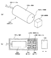
図10(a)及び(b)は、近接センサの外観斜視図と断面図である。
近接センサ1001は、円筒形状でオーステナイト系ステンレス製の筐体1001aに収納され、その先端部分1001bに金属物1002が近接すると、ケーブル1003を通じて所定の論理信号を出力する。
筐体1001aの内部には、回路基板1004と、フェライト製の第一コア1005に収納された検出コイルL1006と、第一コア1005と同一材質且つ同一形状の第二コア1007に収納された参照コイルL1008が、対面状態で収納されている。
10A and 10B are an external perspective view and a cross-sectional view of the proximity sensor.
The
Inside the
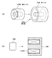
図11(a)及び(b)は、近接センサ1001に用いるコイルとコアの概略図である。
図11(a)は、検出コイルL1006と第一コア1005の分解斜視図である。図11(b)は、検出コイルL1006を収納した第一コア1005の断面図である。なお、参照コイルL1008も検出コイルL1006と同一形状及び同一の電気特性である。
検出コイルL1006を、ボビン形状の第一コア1005に形成された開口部1005aに収納する。こうして第一コア1005に収納された検出コイルL1006は、金属物1002が開口部1005aに近づくと当該金属に渦電流が発生し、この渦電流に起因する損失に応じて検出コイルL1006のインダクタンスが低下する。
FIGS. 11A and 11B are schematic views of a coil and a core used in the
FIG. 11A is an exploded perspective view of the detection coil L1006 and the
The detection coil L1006 is housed in an
[第三の実施形態・近接センサ1001の概念]
図12は、近接センサ1001のブロック図である。図12のブロック図の、図3の変位センサ101と同じ箇所には同一の符号を付して説明を省略する。
図12に示す近接センサ1001の、図3の変位センサ101と異なる点は、電圧検出部304の後にコンパレータが二つ存在することである。
第一コンパレータ1201には、電圧検出部304から出力される変位検出信号が反転入力端子に入力されると共に、電源電圧+Vccを抵抗R1202及び抵抗R1203で分圧した参照電圧が非反転入力端子に入力される。
第二コンパレータ1206には、電圧検出部304から出力される変位検出信号が非反転入力端子に入力されると共に、電源電圧+Vccを抵抗R1207及び抵抗R1208で分圧した参照電圧が反転入力端子に入力される。
第一コンパレータ1201は、電流制限抵抗R1204を通じてオープンコレクタのトランジスタスイッチ1205をオン・オフ制御する。
第二コンパレータ1206は、電流制限抵抗R1209を通じてオープンコレクタのトランジスタスイッチ1210をオン・オフ制御する。
[Third Embodiment / Concept of Proximity Sensor 1001]
FIG. 12 is a block diagram of the
The
In the
In the
The
The
第一の実施形態及び第二の実施形態にて説明した変位センサ101及び変位センサ801は、第一センサコイルL201及び第二センサコイルL202の、インダクタンスの相対的な大小に応じて、電圧検出部304から正負の信号を出力する。
これを近接センサ1001に応用すると、例えば、インダクタンスが固定されている参照コイルL1008に対して検出コイルL1006のインダクタンスが減少すると正極の検出信号を出力するように近接センサ1001が構成されている場合、逆に検出コイルL1006のインダクタンスが増加すると負極の検出信号を出力することとなる。
そこで、検出コイルL1006に非磁性体金属が近接して、検出コイルL1006のインダクタンスが減少することを検出する第一コンパレータ1201と、検出コイルL1006に磁性体金属が近接して、検出コイルL1006のインダクタンスが増加することを検出する第二コンパレータ1206とをそれぞれ設けると、一つの近接センサ1001で二つの状態変化を検出することができる。
勿論、一方のコンパレータを省略して、非磁性体金属のみを検出する近接センサとしても、或は磁性体金属のみを検出する近接センサとしても応用することができる。
The displacement sensor 101 and the displacement sensor 801 described in the first embodiment and the second embodiment include voltage detection units according to the relative magnitudes of the inductances of the first sensor coil L201 and the second sensor coil L202. A positive / negative signal is output from 304.
When this is applied to the
Therefore, the
Of course, one of the comparators can be omitted and applied as a proximity sensor that detects only non-magnetic metal or as a proximity sensor that detects only magnetic metal.
[第三の実施形態・近接センサ1001の回路構成]
図12にて説明したように、変位センサ101の出力信号をコンパレータで二値化することで、近接センサ1001が実現できる。
図13は、本発明の第三の実施形態である近接センサ1001の回路図である。
図13に示す近接センサ1001の回路構成のうち、コンパレータ以前の回路構成は、図4にて説明した、第一の実施形態に係る変位センサ101と同一である。勿論、シーケンサ403の動作も同一であるので、図5及び図6に開示した波形図と同じ動作をする。変位センサ101と異なる点は、第一センサコイルL201は検出コイルL1006となり、第二センサコイルL202は参照コイルL1008となったことである。つまり、検出コイルL1006のインダクタンスは変化するが、参照コイルL1008のインダクタンスは変化しないので、厳密には図5(d)の波形の振幅が少し変化する。しかし、相対的なインダクタンスの差が変化することには変わりがないので、電流差を検出した以降の波形は同一になる。
また、コンパレータ以降の回路構成は、図12の回路素子と全く同一である。したがって、検出コイルL1006のインダクタンスの変化に応じて、非磁性体金属及び磁性体をそれぞれのコンパレータで検出することができる。
[Third Embodiment / Circuit Configuration of Proximity Sensor 1001]
As described in FIG. 12, the
FIG. 13 is a circuit diagram of a
Of the circuit configuration of the
The circuit configuration after the comparator is exactly the same as the circuit element of FIG. Therefore, the nonmagnetic metal and the magnetic material can be detected by the respective comparators according to the change in the inductance of the detection coil L1006.
[第四の実施形態・近接センサ1401の回路構成]
図14は、本発明の第四の実施形態である近接センサ1401の回路図である。
コンパレータ以前の回路構成は、図8にて説明した、第二の実施形態に係る変位センサ801と同一である。勿論、シーケンサ804の動作も同一であるので、図9に開示した波形図と同じ動作をする。
また、第三の実施形態の近接センサ1001と同様、コンパレータ以降の回路構成は、図12の回路素子と全く同一である。したがって、検出コイルL1006のインダクタンスの変化に応じて、非磁性体金属及び磁性体をそれぞれのコンパレータで検出することができる。
[Fourth Embodiment / Circuit Configuration of Proximity Sensor 1401]
FIG. 14 is a circuit diagram of a proximity sensor 1401 according to the fourth embodiment of the present invention.
The circuit configuration before the comparator is the same as that of the displacement sensor 801 according to the second embodiment described with reference to FIG. Of course, since the operation of the
Further, like the
[第五の実施形態・近接センサ1501の回路構成]
第三の実施形態の近接センサ1001及び第四の実施形態に係る近接センサ1401は、それぞれ第一の実施形態に係る変位センサ101及び第二の実施形態に係る変位センサ801の回路をそのまま応用して、近接センサを実現した。変位センサは、プローブ104に対するスリーブ103の位置をアナログ電圧信号にて出力するため、その回路素子には所定の精度(誤差範囲)を要求する。特に、アナログ電圧信号は正負両極方向に変化するので、所定の位置検出精度を実現するため、計測用途に適したオペアンプを正電源と負電源の二電源で駆動させる必要があった。
翻って、近接センサはデジタル値を出力する。つまり、変位センサに求められていた位置検出精度は不要である。非磁性体金属及び/又は磁性体が近接したか否かを検出できさえすればよい。そこで、回路構成をより簡易にするため、図13に開示した近接センサ1001を片電源で実現する構成に作り変えたものが、図15に開示する近接センサ1501である。
[Fifth Embodiment: Circuit Configuration of Proximity Sensor 1501]
The
In turn, the proximity sensor outputs a digital value. That is, the position detection accuracy required for the displacement sensor is unnecessary. It is only necessary to detect whether or not the nonmagnetic metal and / or the magnetic material are close to each other. Therefore, in order to make the circuit configuration simpler, a proximity sensor 1501 disclosed in FIG. 15 is changed to a configuration in which the
図15は、本発明の第五の実施形態である近接センサ1501の回路図である。
図15に示す近接センサ1501の回路構成のうち、図13に示す近接センサ1001の回路構成との相違点は、第一矩形波電圧源401、第二矩形波電圧源402及びシーケンサ403をマイコン1511で実現している点と、オペアンプ404及びオペアンプ407を片電源で動作させるために、非反転入力端子に抵抗R1504及び抵抗R1505で電源電圧を分圧して、電源電圧の半分の電位を与えている点である。
検出コイルL1006には、マイコン1511から出力される矩形波信号がコンデンサC1509を介して入力される。同様に参照コイルL1008には、マイコン1511から出力される矩形波信号がコンデンサC1510を介して入力される。市場に流通する一般的なマイコン1511は例えば+5Vの片電源仕様であるので、マイコン1511のバスから出力される矩形波信号は、0Vと5Vしか出力しない。そこで、コンデンサC1509及びC1510で直流成分をカットして、検出コイルL1006及び参照コイルL1008に矩形波信号の交流成分のみ供給する。
図15の回路は、仮に変位センサとして用いると変位検出精度の点では劣るものの、金属物或は磁性体を検出する用途であれば十分な性能を発揮する。また、片電源仕様であり、市販のマイコン1511をそのまま用いることができるので、極めて安価に近接センサ1501を実現することができる。
FIG. 15 is a circuit diagram of a proximity sensor 1501 according to the fifth embodiment of the present invention.
15 differs from the circuit configuration of the
A rectangular wave signal output from the
Although the circuit of FIG. 15 is inferior in terms of displacement detection accuracy if used as a displacement sensor, it exhibits sufficient performance for use in detecting a metal object or a magnetic material. Moreover, since it is a single power supply specification and the commercially
本実施形態では、変位センサ及び近接センサを開示した。
第一乃至第五の実施形態に共通する技術として、二つのコイルに矩形波電圧を印加して、各々のコイルに流れる電流を独立して検出してから差動回路等で差を演算するのではなく、直接電流の差の値を検出することにより、S/N比が良好であり高感度なセンサを実現できる。
また、各々のコイルは同じ磁気特性と電気特性を備えるため、温度変化でこれらの特性が変化したとしても夫々同じように変化するので、温度変化に起因するばらつきが生じ難い。
In the present embodiment, a displacement sensor and a proximity sensor have been disclosed.
As a technique common to the first to fifth embodiments, a rectangular wave voltage is applied to two coils, a current flowing through each coil is independently detected, and then a difference is calculated by a differential circuit or the like. Instead, by directly detecting the value of the current difference, a sensor with a good S / N ratio and high sensitivity can be realized.
In addition, since each coil has the same magnetic characteristics and electrical characteristics, even if these characteristics change due to a temperature change, they change in the same way, so that variations due to the temperature change hardly occur.
第一の実施形態に係る変位センサ101は、二つのセンサコイルに矩形波交流電圧を与え、その電流差を電圧信号に変換して、交流直流変換を施すことと、矩形波交流電圧は低く抑え、その代わりに矩形波交流の周期を大きく設定することで、センサコイルを感度が低下してしまう金属製の外殻104aに収納しても、必要十分な位置検出感度を得ることができる。 The displacement sensor 101 according to the first embodiment applies a rectangular wave AC voltage to two sensor coils, converts the current difference into a voltage signal, performs AC / DC conversion, and keeps the rectangular wave AC voltage low. Instead, by setting the period of the rectangular wave AC to be large, even if the sensor coil is housed in the metal outer shell 104a whose sensitivity is lowered, necessary and sufficient position detection sensitivity can be obtained.
第二の実施形態に係る変位センサ801も、第一の実施形態に係る変位センサ101と同様に、センサコイルを感度が低下してしまう金属製の外殻104aに収納しても、必要十分な位置検出感度を得ることができる。更に、第二の実施形態に係る変位センサ801は、カレントトランス803を採用することで、二つのセンサコイルをケーブルで延長する用途に適している。
Similarly to the displacement sensor 101 according to the first embodiment, the displacement sensor 801 according to the second embodiment is necessary and sufficient even if the sensor coil is housed in the metal outer shell 104a whose sensitivity decreases. Position detection sensitivity can be obtained. Furthermore, the displacement sensor 801 according to the second embodiment is suitable for an application in which two sensor coils are extended with a cable by adopting a
第三の実施形態に係る近接センサ1001は、二つのコイルに矩形波交流電圧を与え、その電流差を電圧信号に変換して、交流直流変換を施すことと、矩形波交流電圧は低く抑え、その代わりに矩形波交流の周期を大きく設定することで、検出コイルL1006を感度が低下してしまう金属製の筐体1001aに収納しても、必要十分な金属物或は磁性体が近接したことを検出する感度を得ることができる。
The
第四の実施形態に係る近接センサ1401も、第三の実施形態に係る近接センサ1001と同様に、検出コイルL1006を感度が低下してしまう金属製の筐体1001aに収納しても、必要十分な金属物或は磁性体が近接したことを検出する感度を得ることができる。更に、第四の実施形態に係る近接センサ1401は、第二の実施形態に係る変位センサ801と同様にカレントトランス803を採用することで、検出コイルL1006をケーブルで延長する用途に適している。
Similar to the
第五の実施形態に係る近接センサ1501も、第三の実施形態に係る近接センサ1001と同様に、検出コイルL1006を感度が低下してしまう金属製の筐体1001aに収納しても、必要十分な金属物或は磁性体が近接したことを検出する感度を得ることができる。更に、第五の実施形態に係る近接センサ1501は、片電源仕様にすることで回路構成が簡素になると共に、回路素子の精度に余裕ができるので、低コストの近接センサを実現できる。
Similar to the
以上、本発明の実施形態例について説明したが、本発明は上記実施形態例に限定されるものではなく、特許請求の範囲に記載した本発明の要旨を逸脱しない限りにおいて、他の変形例、応用例を含む。 The embodiment of the present invention has been described above. However, the present invention is not limited to the above-described embodiment, and other modifications may be made without departing from the gist of the present invention described in the claims. Includes application examples.
101…変位センサ、102…センサ本体部、103…スリーブ、104…プローブ、105…筐体、203…コア、L201…第一センサコイル、L202…第二センサコイル、301…矩形波電圧源、302…電流差検出部、303…反転増幅回路、304…電圧検出部、401…第一矩形波電圧源、402…第二矩形波電圧源、403…シーケンサ、404…オペアンプ、407…オペアンプ、409…アナログスイッチ、412…変位検出部、701…変位検出部、702…トランス、704…モノマルチ、705…モノマルチ、706…スイッチ、708…オペアンプ、710…スイッチ、712…オペアンプ、801…変位センサ、802…矩形波電圧源、803…カレントトランス、804…シーケンサ、1001…近接センサ、1002…金属物、1003…ケーブル、1004…回路基板、1005…第一コア、L1006…検出コイル、1007…第二コア、L1008…参照コイル、1201…第一コンパレータ、1205…トランジスタスイッチ、1206…第二コンパレータ、1210…トランジスタスイッチ、1401…近接センサ、1501…近接センサ、1511…マイコン
DESCRIPTION OF SYMBOLS 101 ...
周知のとおり、オーステナイト系のステンレスは剛性が高い非磁性体金属であり、更に抵抗率が高いので、プローブ104に用いる場合、抵抗率の低い金属と比べると渦電流を小さく抑えることができる。しかしながら、抵抗率が高いとはいえどもステンレスは導体であるので、コイルに交流電流を流した際に渦電流の発生は免れない。渦電流は熱エネルギーに変換され、結果としてコイルのインダクタンスの低下を招く。
なお、プローブ104の外殻104aの材質は、必ずしもステンレスに限られないが、一定の条件が求められる。前述のように、非磁性体金属であることと、抵抗率が高いことである。抵抗率は、スリーブ103の抵抗率より高いことが好ましい。本実施形態の場合はスリーブ103の材質である真鍮(黄銅)が5〜7×10⁻⁸ Ωmであるのに対し、ステンレスは7.2×10⁻⁷ Ωmなので、この条件を満たす。
As is well known, austenitic stainless steel is a non-magnetic metal having high rigidity and has a high resistivity. Therefore, when used for the probe 104, the eddy current can be suppressed to be smaller than that of a metal having a low resistivity. However, although stainless steel is a conductor even though the resistivity is high, generation of eddy current is inevitable when an alternating current is passed through the coil. Eddy currents are converted into thermal energy, resulting in a reduction in coil inductance.
The material of the outer shell 104a of the probe 104 is not necessarily limited to stainless steel, but certain conditions are required. As described above, it is a non-magnetic metal and has a high resistivity. The resistivity is preferably higher than the resistivity of the
Claims (4)
第二センサコイルと、
前記第一センサコイル及び/又は第二センサコイルのインダクタンスを変化させる金属製のスリーブと、
前記第一センサコイル及び前記第二センサコイルに矩形波電圧を供給する矩形波電圧源と、
前記第一センサコイルに流れる第一の電流と、前記第二センサコイルに流れる第二の電流との差を検出して電圧信号を出力する電流差検出部と、
前記電流差検出部から得られる電流差信号の電位を反転する反転増幅回路と、
前記電流差信号と前記反転増幅回路の出力信号を基に前記第一センサコイル及び前記第二センサコイルの相対的インダクタンスの差に応じて変化する信号を出力する電圧検出部と
を具備する変位センサ。 A first sensor coil;
A second sensor coil;
A metal sleeve for changing the inductance of the first sensor coil and / or the second sensor coil;
A rectangular wave voltage source for supplying a rectangular wave voltage to the first sensor coil and the second sensor coil;
A current difference detector that detects a difference between a first current flowing through the first sensor coil and a second current flowing through the second sensor coil and outputs a voltage signal;
An inverting amplifier circuit for inverting the potential of the current difference signal obtained from the current difference detection unit;
A displacement sensor comprising: a voltage detection unit that outputs a signal that changes in accordance with a difference in relative inductance between the first sensor coil and the second sensor coil based on the current difference signal and an output signal of the inverting amplifier circuit. .
前記第一センサコイル及び前記第二センサコイルが長手方向に巻線される高透磁率のコアと、
前記第一センサコイル及び前記第二センサコイルを収納する金属製の外殻と
を具備し、
前記スリーブは前記金属製の外殻を覆う形状であると共に、前記スリーブの抵抗率は前記外殻の抵抗率より小さい、
請求項1記載の変位センサ。 Furthermore,
A high permeability core around which the first sensor coil and the second sensor coil are wound in the longitudinal direction;
A metal outer shell that houses the first sensor coil and the second sensor coil;
The sleeve has a shape covering the metal outer shell, and the resistivity of the sleeve is smaller than the resistivity of the outer shell,
The displacement sensor according to claim 1.
前記第一センサコイルと前記第二センサコイルは前記オペアンプの反転入力端子に接続される、
請求項2記載の変位センサ。 The current difference detection unit is an operational amplifier,
The first sensor coil and the second sensor coil are connected to an inverting input terminal of the operational amplifier.
The displacement sensor according to claim 2.
前記第一センサコイルは前記トランスの第一巻線に接続され、
前記第二センサコイルは前記トランスの前記第一巻線と同一巻線数の第二巻線に接続され、
前記オペアンプの反転入力端子及び非反転入力端子はそれぞれ前記トランスの第三巻線に接続される、
請求項2記載の変位センサ。 The current difference detection unit is a transformer and an operational amplifier,
The first sensor coil is connected to the first winding of the transformer;
The second sensor coil is connected to a second winding having the same number of windings as the first winding of the transformer,
The inverting input terminal and the non-inverting input terminal of the operational amplifier are respectively connected to the third winding of the transformer.
The displacement sensor according to claim 2.
Priority Applications (1)
| Application Number | Priority Date | Filing Date | Title |
|---|---|---|---|
| JP2011048173A JP4852666B1 (en) | 2011-03-04 | 2011-03-04 | Displacement sensor |
Applications Claiming Priority (1)
| Application Number | Priority Date | Filing Date | Title |
|---|---|---|---|
| JP2011048173A JP4852666B1 (en) | 2011-03-04 | 2011-03-04 | Displacement sensor |
Publications (2)
| Publication Number | Publication Date |
|---|---|
| JP4852666B1 JP4852666B1 (en) | 2012-01-11 |
| JP2012185032A true JP2012185032A (en) | 2012-09-27 |
Family
ID=45540510
Family Applications (1)
| Application Number | Title | Priority Date | Filing Date |
|---|---|---|---|
| JP2011048173A Active JP4852666B1 (en) | 2011-03-04 | 2011-03-04 | Displacement sensor |
Country Status (1)
| Country | Link |
|---|---|
| JP (1) | JP4852666B1 (en) |
Cited By (1)
| Publication number | Priority date | Publication date | Assignee | Title |
|---|---|---|---|---|
| KR101751485B1 (en) * | 2015-03-10 | 2017-06-27 | 주식회사 트루윈 | Inductive Displacement Sensor Using Amplitude Modulation |
Families Citing this family (2)
| Publication number | Priority date | Publication date | Assignee | Title |
|---|---|---|---|---|
| CN112284230B (en) * | 2020-10-09 | 2021-11-16 | 珠海格力电器股份有限公司 | Displacement detection device, displacement monitoring method and compressor |
| CN114440753B (en) * | 2022-02-24 | 2022-11-22 | 电子科技大学 | Non-contact displacement measuring device based on eddy current principle |
Citations (33)
| Publication number | Priority date | Publication date | Assignee | Title |
|---|---|---|---|---|
| JPS5276055A (en) * | 1975-12-22 | 1977-06-25 | Bon Denki Kk | Device for detecting uneveness of surface of banddlike object |
| JPS549652A (en) * | 1977-06-22 | 1979-01-24 | Matsushita Electric Works Ltd | Differential transformer type sensor |
| JPS5544950A (en) * | 1978-09-25 | 1980-03-29 | Shin Meiwa Ind Co Ltd | Electromagnetic sensing method and sensor |
| JPS566488A (en) * | 1979-06-28 | 1981-01-23 | Toshiba Corp | Oxide piezo-electric material |
| JPS57207804A (en) * | 1981-06-17 | 1982-12-20 | Japanese National Railways<Jnr> | Spot detecting device of vehicle |
| JPS58206918A (en) * | 1982-01-29 | 1983-12-02 | Komatsu Ltd | Signal processing circuit of differential transformer |
| JPS5910814A (en) * | 1982-07-12 | 1984-01-20 | Hitachi Metals Ltd | Level sensor for toner |
| JPS6018701A (en) * | 1983-07-13 | 1985-01-30 | Anritsu Corp | Displacement measuring device |
| JPS6049404U (en) * | 1983-09-12 | 1985-04-06 | 株式会社ミツトヨ | Displacement measuring device |
| JPS6146463U (en) * | 1984-08-30 | 1986-03-28 | ティーディーケイ株式会社 | magnetic sensing device |
| JPS61284608A (en) * | 1985-06-11 | 1986-12-15 | Shin Meiwa Ind Co Ltd | Signal processing unit for differential transformer |
| JPS6222002A (en) * | 1985-07-22 | 1987-01-30 | Mitsutoyo Mfg Corp | Displacement detection head |
| JPS6253373U (en) * | 1985-09-25 | 1987-04-02 | ||
| JPS63163114A (en) * | 1986-12-25 | 1988-07-06 | Sanki Eng Co Ltd | Displacement detector |
| JPS63252258A (en) * | 1987-04-09 | 1988-10-19 | Diesel Kiki Co Ltd | Detector of acceleration caused by vibration |
| JPS63273001A (en) * | 1987-04-30 | 1988-11-10 | Makome Kenkyusho:Kk | Displacement measuring instrument |
| JPH0158163U (en) * | 1987-10-08 | 1989-04-11 | ||
| JPH01202670A (en) * | 1988-02-09 | 1989-08-15 | Diesel Kiki Co Ltd | Three-dimensional acceleration sensor |
| JPH02201114A (en) * | 1989-01-30 | 1990-08-09 | Makome Kenkyusho:Kk | Displacement measuring device |
| JPH0518406A (en) * | 1991-07-11 | 1993-01-26 | Yamaha Motor Co Ltd | Oil-hydraulic apparatus with stroke sensor |
| JPH0577604U (en) * | 1992-03-23 | 1993-10-22 | 株式会社南武 | Rotary cylinder rod position detector |
| JPH05280914A (en) * | 1992-03-31 | 1993-10-29 | Isuzu Motors Ltd | Detection sensor of amount of displacement |
| JPH06331303A (en) * | 1993-05-26 | 1994-12-02 | I T W Ind Kk | Detection of quantity of displacement of core |
| JPH0755499A (en) * | 1993-08-13 | 1995-03-03 | Sakata Denki Kk | Device for measuring displacement |
| JPH07234102A (en) * | 1994-02-25 | 1995-09-05 | Reideitsuku:Kk | Displacement measuring apparatus |
| JPH07270178A (en) * | 1994-03-29 | 1995-10-20 | Japan Steel Works Ltd:The | Apparatus for detecting position of core of differential transformer |
| JPH1038090A (en) * | 1996-07-22 | 1998-02-13 | Koyo Electron Ind Co Ltd | Waterproof structure in integrally molded product by metal member and resin |
| JP2001027505A (en) * | 1999-07-13 | 2001-01-30 | Ribekkusu:Kk | Position transducer for small fluid pressure cylinder |
| JP2001356179A (en) * | 2000-06-13 | 2001-12-26 | S G:Kk | Conductor detection device |
| JP2005031245A (en) * | 2003-07-09 | 2005-02-03 | Kyocera Mita Corp | Image forming apparatus |
| JP2005201790A (en) * | 2004-01-16 | 2005-07-28 | Keyence Corp | Contact type displacement measuring instrument |
| JP2008170360A (en) * | 2007-01-15 | 2008-07-24 | Shinko Denki Kk | Displacement sensor |
| JP2010216863A (en) * | 2009-03-13 | 2010-09-30 | Yamatake Corp | Proximity sensor |
Family Cites Families (4)
| Publication number | Priority date | Publication date | Assignee | Title |
|---|---|---|---|---|
| JPS6049404A (en) * | 1983-08-30 | 1985-03-18 | Toshiba Mach Co Ltd | Simulator of system to be controlled of temperature controller |
| JPS6146463A (en) * | 1984-08-09 | 1986-03-06 | Nippon Denso Co Ltd | Starter |
| EP0214792A3 (en) * | 1985-08-29 | 1988-03-02 | The Research Foundation Of State University Of New York | Polymer alloys of aminopolysiloxanes with brominated derivatives of polyphenylene oxide |
| JPS6458163A (en) * | 1987-08-28 | 1989-03-06 | Minolta Camera Kk | Picture reader having magnification function |
-
2011
- 2011-03-04 JP JP2011048173A patent/JP4852666B1/en active Active
Patent Citations (33)
| Publication number | Priority date | Publication date | Assignee | Title |
|---|---|---|---|---|
| JPS5276055A (en) * | 1975-12-22 | 1977-06-25 | Bon Denki Kk | Device for detecting uneveness of surface of banddlike object |
| JPS549652A (en) * | 1977-06-22 | 1979-01-24 | Matsushita Electric Works Ltd | Differential transformer type sensor |
| JPS5544950A (en) * | 1978-09-25 | 1980-03-29 | Shin Meiwa Ind Co Ltd | Electromagnetic sensing method and sensor |
| JPS566488A (en) * | 1979-06-28 | 1981-01-23 | Toshiba Corp | Oxide piezo-electric material |
| JPS57207804A (en) * | 1981-06-17 | 1982-12-20 | Japanese National Railways<Jnr> | Spot detecting device of vehicle |
| JPS58206918A (en) * | 1982-01-29 | 1983-12-02 | Komatsu Ltd | Signal processing circuit of differential transformer |
| JPS5910814A (en) * | 1982-07-12 | 1984-01-20 | Hitachi Metals Ltd | Level sensor for toner |
| JPS6018701A (en) * | 1983-07-13 | 1985-01-30 | Anritsu Corp | Displacement measuring device |
| JPS6049404U (en) * | 1983-09-12 | 1985-04-06 | 株式会社ミツトヨ | Displacement measuring device |
| JPS6146463U (en) * | 1984-08-30 | 1986-03-28 | ティーディーケイ株式会社 | magnetic sensing device |
| JPS61284608A (en) * | 1985-06-11 | 1986-12-15 | Shin Meiwa Ind Co Ltd | Signal processing unit for differential transformer |
| JPS6222002A (en) * | 1985-07-22 | 1987-01-30 | Mitsutoyo Mfg Corp | Displacement detection head |
| JPS6253373U (en) * | 1985-09-25 | 1987-04-02 | ||
| JPS63163114A (en) * | 1986-12-25 | 1988-07-06 | Sanki Eng Co Ltd | Displacement detector |
| JPS63252258A (en) * | 1987-04-09 | 1988-10-19 | Diesel Kiki Co Ltd | Detector of acceleration caused by vibration |
| JPS63273001A (en) * | 1987-04-30 | 1988-11-10 | Makome Kenkyusho:Kk | Displacement measuring instrument |
| JPH0158163U (en) * | 1987-10-08 | 1989-04-11 | ||
| JPH01202670A (en) * | 1988-02-09 | 1989-08-15 | Diesel Kiki Co Ltd | Three-dimensional acceleration sensor |
| JPH02201114A (en) * | 1989-01-30 | 1990-08-09 | Makome Kenkyusho:Kk | Displacement measuring device |
| JPH0518406A (en) * | 1991-07-11 | 1993-01-26 | Yamaha Motor Co Ltd | Oil-hydraulic apparatus with stroke sensor |
| JPH0577604U (en) * | 1992-03-23 | 1993-10-22 | 株式会社南武 | Rotary cylinder rod position detector |
| JPH05280914A (en) * | 1992-03-31 | 1993-10-29 | Isuzu Motors Ltd | Detection sensor of amount of displacement |
| JPH06331303A (en) * | 1993-05-26 | 1994-12-02 | I T W Ind Kk | Detection of quantity of displacement of core |
| JPH0755499A (en) * | 1993-08-13 | 1995-03-03 | Sakata Denki Kk | Device for measuring displacement |
| JPH07234102A (en) * | 1994-02-25 | 1995-09-05 | Reideitsuku:Kk | Displacement measuring apparatus |
| JPH07270178A (en) * | 1994-03-29 | 1995-10-20 | Japan Steel Works Ltd:The | Apparatus for detecting position of core of differential transformer |
| JPH1038090A (en) * | 1996-07-22 | 1998-02-13 | Koyo Electron Ind Co Ltd | Waterproof structure in integrally molded product by metal member and resin |
| JP2001027505A (en) * | 1999-07-13 | 2001-01-30 | Ribekkusu:Kk | Position transducer for small fluid pressure cylinder |
| JP2001356179A (en) * | 2000-06-13 | 2001-12-26 | S G:Kk | Conductor detection device |
| JP2005031245A (en) * | 2003-07-09 | 2005-02-03 | Kyocera Mita Corp | Image forming apparatus |
| JP2005201790A (en) * | 2004-01-16 | 2005-07-28 | Keyence Corp | Contact type displacement measuring instrument |
| JP2008170360A (en) * | 2007-01-15 | 2008-07-24 | Shinko Denki Kk | Displacement sensor |
| JP2010216863A (en) * | 2009-03-13 | 2010-09-30 | Yamatake Corp | Proximity sensor |
Cited By (1)
| Publication number | Priority date | Publication date | Assignee | Title |
|---|---|---|---|---|
| KR101751485B1 (en) * | 2015-03-10 | 2017-06-27 | 주식회사 트루윈 | Inductive Displacement Sensor Using Amplitude Modulation |
Also Published As
| Publication number | Publication date |
|---|---|
| JP4852666B1 (en) | 2012-01-11 |
Similar Documents
| Publication | Publication Date | Title |
|---|---|---|
| JP6304647B2 (en) | Current detector | |
| JP2014117153A (en) | Estimation of resistance in electrical machine | |
| JP2011017632A (en) | Flux gate leakage sensor | |
| US20180292235A1 (en) | Measuring the position of an object using eddy-currents | |
| JP2010533856A5 (en) | ||
| CN107407576B (en) | Induction type movable sensor | |
| CN106950515A (en) | Magnetic Sensor and the current sensor for possessing it | |
| JP4852666B1 (en) | Displacement sensor | |
| JP5814976B2 (en) | Current measuring device | |
| JP4852667B1 (en) | Proximity sensor | |
| JP4623289B2 (en) | Current sensor | |
| JP2013120098A (en) | Voltage detection apparatus and power detection apparatus | |
| JP4209114B2 (en) | Magnetic field sensor | |
| JP2008164449A (en) | Current sensor | |
| JP6106909B2 (en) | Current sensor | |
| Wang et al. | Split core closed loop Hall effect current sensors and applications | |
| Qing et al. | An innovative combined electronic instrument transformer applied in high voltage lines | |
| JP7262885B2 (en) | Ultra-sensitive micro magnetic sensor | |
| JP5767673B2 (en) | Current waveform measuring device | |
| JP2011112634A (en) | Ring core for flux gate leakage sensor, ring core unit including the ring core, and the flux gate leakage sensor | |
| JP4810021B2 (en) | Position detection device | |
| JP4731633B1 (en) | Magnetic sensor | |
| JP4747224B1 (en) | Inductance change detection circuit, displacement detection device, and metal detection device | |
| JP4898971B1 (en) | Inductance change detection circuit, displacement detection device, and metal detection device | |
| KR100828737B1 (en) | Linear variable differential transformer |
Legal Events
| Date | Code | Title | Description |
|---|---|---|---|
| TRDD | Decision of grant or rejection written | ||
| A01 | Written decision to grant a patent or to grant a registration (utility model) |
Free format text: JAPANESE INTERMEDIATE CODE: A01 |
|
| A61 | First payment of annual fees (during grant procedure) |
Free format text: JAPANESE INTERMEDIATE CODE: A61 Effective date: 20111024 |
|
| R150 | Certificate of patent or registration of utility model |
Ref document number: 4852666 Country of ref document: JP Free format text: JAPANESE INTERMEDIATE CODE: R150 Free format text: JAPANESE INTERMEDIATE CODE: R150 |
|
| FPAY | Renewal fee payment (event date is renewal date of database) |
Free format text: PAYMENT UNTIL: 20141028 Year of fee payment: 3 |
|
| R250 | Receipt of annual fees |
Free format text: JAPANESE INTERMEDIATE CODE: R250 |
|
| R250 | Receipt of annual fees |
Free format text: JAPANESE INTERMEDIATE CODE: R250 |
|
| R250 | Receipt of annual fees |
Free format text: JAPANESE INTERMEDIATE CODE: R250 |
|
| R250 | Receipt of annual fees |
Free format text: JAPANESE INTERMEDIATE CODE: R250 |
|
| R250 | Receipt of annual fees |
Free format text: JAPANESE INTERMEDIATE CODE: R250 |
|
| R250 | Receipt of annual fees |
Free format text: JAPANESE INTERMEDIATE CODE: R250 |
|
| R250 | Receipt of annual fees |
Free format text: JAPANESE INTERMEDIATE CODE: R250 |
|
| R250 | Receipt of annual fees |
Free format text: JAPANESE INTERMEDIATE CODE: R250 |
|
| R250 | Receipt of annual fees |
Free format text: JAPANESE INTERMEDIATE CODE: R250 |
|
| R250 | Receipt of annual fees |
Free format text: JAPANESE INTERMEDIATE CODE: R250 |