JP2012175067A - Image pickup device, and manufacturing method therefor, and electronic apparatus - Google Patents
Image pickup device, and manufacturing method therefor, and electronic apparatus Download PDFInfo
- Publication number
- JP2012175067A JP2012175067A JP2011038668A JP2011038668A JP2012175067A JP 2012175067 A JP2012175067 A JP 2012175067A JP 2011038668 A JP2011038668 A JP 2011038668A JP 2011038668 A JP2011038668 A JP 2011038668A JP 2012175067 A JP2012175067 A JP 2012175067A
- Authority
- JP
- Japan
- Prior art keywords
- solid
- imaging device
- gate electrode
- state imaging
- substrate
- Prior art date
- Legal status (The legal status is an assumption and is not a legal conclusion. Google has not performed a legal analysis and makes no representation as to the accuracy of the status listed.)
- Ceased
Links
- 238000004519 manufacturing process Methods 0.000 title claims description 23
- 239000000758 substrate Substances 0.000 claims abstract description 158
- 239000004065 semiconductor Substances 0.000 claims abstract description 131
- 238000003384 imaging method Methods 0.000 claims abstract description 126
- 239000007769 metal material Substances 0.000 claims description 15
- 229910052735 hafnium Inorganic materials 0.000 claims description 10
- RTAQQCXQSZGOHL-UHFFFAOYSA-N Titanium Chemical compound [Ti] RTAQQCXQSZGOHL-UHFFFAOYSA-N 0.000 claims description 9
- 229910052782 aluminium Inorganic materials 0.000 claims description 9
- XAGFODPZIPBFFR-UHFFFAOYSA-N aluminium Chemical compound [Al] XAGFODPZIPBFFR-UHFFFAOYSA-N 0.000 claims description 9
- 239000010936 titanium Substances 0.000 claims description 9
- 229910052719 titanium Inorganic materials 0.000 claims description 9
- XUIMIQQOPSSXEZ-UHFFFAOYSA-N Silicon Chemical compound [Si] XUIMIQQOPSSXEZ-UHFFFAOYSA-N 0.000 claims description 8
- VBJZVLUMGGDVMO-UHFFFAOYSA-N hafnium atom Chemical compound [Hf] VBJZVLUMGGDVMO-UHFFFAOYSA-N 0.000 claims description 8
- 229910052710 silicon Inorganic materials 0.000 claims description 8
- 239000010703 silicon Substances 0.000 claims description 8
- 229910052715 tantalum Inorganic materials 0.000 claims description 8
- GUVRBAGPIYLISA-UHFFFAOYSA-N tantalum atom Chemical compound [Ta] GUVRBAGPIYLISA-UHFFFAOYSA-N 0.000 claims description 8
- 239000000463 material Substances 0.000 claims description 7
- WFKWXMTUELFFGS-UHFFFAOYSA-N tungsten Chemical compound [W] WFKWXMTUELFFGS-UHFFFAOYSA-N 0.000 claims description 6
- 229910052721 tungsten Inorganic materials 0.000 claims description 6
- 239000010937 tungsten Substances 0.000 claims description 6
- 229910017052 cobalt Inorganic materials 0.000 claims description 5
- 239000010941 cobalt Substances 0.000 claims description 5
- GUTLYIVDDKVIGB-UHFFFAOYSA-N cobalt atom Chemical compound [Co] GUTLYIVDDKVIGB-UHFFFAOYSA-N 0.000 claims description 5
- OAICVXFJPJFONN-UHFFFAOYSA-N Phosphorus Chemical compound [P] OAICVXFJPJFONN-UHFFFAOYSA-N 0.000 claims description 3
- VYPSYNLAJGMNEJ-UHFFFAOYSA-N Silicium dioxide Chemical compound O=[Si]=O VYPSYNLAJGMNEJ-UHFFFAOYSA-N 0.000 claims description 3
- 229910021417 amorphous silicon Inorganic materials 0.000 claims description 3
- 229910052746 lanthanum Inorganic materials 0.000 claims description 3
- FZLIPJUXYLNCLC-UHFFFAOYSA-N lanthanum atom Chemical compound [La] FZLIPJUXYLNCLC-UHFFFAOYSA-N 0.000 claims description 3
- 229910052698 phosphorus Inorganic materials 0.000 claims description 3
- 239000011574 phosphorus Substances 0.000 claims description 3
- 229910052814 silicon oxide Inorganic materials 0.000 claims description 3
- OKTJSMMVPCPJKN-UHFFFAOYSA-N Carbon Chemical compound [C] OKTJSMMVPCPJKN-UHFFFAOYSA-N 0.000 claims description 2
- 229910021389 graphene Inorganic materials 0.000 claims description 2
- AMGQUBHHOARCQH-UHFFFAOYSA-N indium;oxotin Chemical compound [In].[Sn]=O AMGQUBHHOARCQH-UHFFFAOYSA-N 0.000 claims description 2
- 229910021332 silicide Inorganic materials 0.000 claims description 2
- FVBUAEGBCNSCDD-UHFFFAOYSA-N silicide(4-) Chemical compound [Si-4] FVBUAEGBCNSCDD-UHFFFAOYSA-N 0.000 claims description 2
- 229910006404 SnO 2 Inorganic materials 0.000 claims 1
- 239000007787 solid Substances 0.000 abstract 1
- 239000010408 film Substances 0.000 description 146
- 239000010410 layer Substances 0.000 description 15
- 238000012986 modification Methods 0.000 description 15
- 230000004048 modification Effects 0.000 description 15
- 238000000034 method Methods 0.000 description 9
- 230000002093 peripheral effect Effects 0.000 description 8
- 238000006243 chemical reaction Methods 0.000 description 7
- GWEVSGVZZGPLCZ-UHFFFAOYSA-N Titan oxide Chemical compound O=[Ti]=O GWEVSGVZZGPLCZ-UHFFFAOYSA-N 0.000 description 6
- 230000003287 optical effect Effects 0.000 description 5
- 230000000149 penetrating effect Effects 0.000 description 5
- 230000035515 penetration Effects 0.000 description 5
- 230000006870 function Effects 0.000 description 4
- 229910000449 hafnium oxide Inorganic materials 0.000 description 4
- WIHZLLGSGQNAGK-UHFFFAOYSA-N hafnium(4+);oxygen(2-) Chemical compound [O-2].[O-2].[Hf+4] WIHZLLGSGQNAGK-UHFFFAOYSA-N 0.000 description 4
- BPUBBGLMJRNUCC-UHFFFAOYSA-N oxygen(2-);tantalum(5+) Chemical compound [O-2].[O-2].[O-2].[O-2].[O-2].[Ta+5].[Ta+5] BPUBBGLMJRNUCC-UHFFFAOYSA-N 0.000 description 4
- RVTZCBVAJQQJTK-UHFFFAOYSA-N oxygen(2-);zirconium(4+) Chemical compound [O-2].[O-2].[Zr+4] RVTZCBVAJQQJTK-UHFFFAOYSA-N 0.000 description 4
- 238000005498 polishing Methods 0.000 description 4
- 229910001936 tantalum oxide Inorganic materials 0.000 description 4
- 239000010409 thin film Substances 0.000 description 4
- 229910001928 zirconium oxide Inorganic materials 0.000 description 4
- 238000001312 dry etching Methods 0.000 description 3
- 238000005530 etching Methods 0.000 description 3
- 230000031700 light absorption Effects 0.000 description 3
- 241000588731 Hafnia Species 0.000 description 2
- BPQQTUXANYXVAA-UHFFFAOYSA-N Orthosilicate Chemical compound [O-][Si]([O-])([O-])[O-] BPQQTUXANYXVAA-UHFFFAOYSA-N 0.000 description 2
- 238000000231 atomic layer deposition Methods 0.000 description 2
- 238000000701 chemical imaging Methods 0.000 description 2
- 238000010586 diagram Methods 0.000 description 2
- 238000009792 diffusion process Methods 0.000 description 2
- 230000005684 electric field Effects 0.000 description 2
- -1 hafnium aluminate Chemical class 0.000 description 2
- CJNBYAVZURUTKZ-UHFFFAOYSA-N hafnium(IV) oxide Inorganic materials O=[Hf]=O CJNBYAVZURUTKZ-UHFFFAOYSA-N 0.000 description 2
- 238000005468 ion implantation Methods 0.000 description 2
- 230000001590 oxidative effect Effects 0.000 description 2
- TWNQGVIAIRXVLR-UHFFFAOYSA-N oxo(oxoalumanyloxy)alumane Chemical compound O=[Al]O[Al]=O TWNQGVIAIRXVLR-UHFFFAOYSA-N 0.000 description 2
- SIWVEOZUMHYXCS-UHFFFAOYSA-N oxo(oxoyttriooxy)yttrium Chemical compound O=[Y]O[Y]=O SIWVEOZUMHYXCS-UHFFFAOYSA-N 0.000 description 2
- MMKQUGHLEMYQSG-UHFFFAOYSA-N oxygen(2-);praseodymium(3+) Chemical compound [O-2].[O-2].[O-2].[Pr+3].[Pr+3] MMKQUGHLEMYQSG-UHFFFAOYSA-N 0.000 description 2
- 229910003447 praseodymium oxide Inorganic materials 0.000 description 2
- 239000002210 silicon-based material Substances 0.000 description 2
- 239000000243 solution Substances 0.000 description 2
- 239000000126 substance Substances 0.000 description 2
- XOLBLPGZBRYERU-UHFFFAOYSA-N tin dioxide Chemical compound O=[Sn]=O XOLBLPGZBRYERU-UHFFFAOYSA-N 0.000 description 2
- 239000004408 titanium dioxide Substances 0.000 description 2
- OGIDPMRJRNCKJF-UHFFFAOYSA-N titanium oxide Inorganic materials [Ti]=O OGIDPMRJRNCKJF-UHFFFAOYSA-N 0.000 description 2
- VHUUQVKOLVNVRT-UHFFFAOYSA-N Ammonium hydroxide Chemical compound [NH4+].[OH-] VHUUQVKOLVNVRT-UHFFFAOYSA-N 0.000 description 1
- ZAMOUSCENKQFHK-UHFFFAOYSA-N Chlorine atom Chemical compound [Cl] ZAMOUSCENKQFHK-UHFFFAOYSA-N 0.000 description 1
- MHAJPDPJQMAIIY-UHFFFAOYSA-N Hydrogen peroxide Chemical compound OO MHAJPDPJQMAIIY-UHFFFAOYSA-N 0.000 description 1
- 238000009825 accumulation Methods 0.000 description 1
- 239000000853 adhesive Substances 0.000 description 1
- 230000001070 adhesive effect Effects 0.000 description 1
- 230000002411 adverse Effects 0.000 description 1
- 239000000908 ammonium hydroxide Substances 0.000 description 1
- 230000003321 amplification Effects 0.000 description 1
- 238000000137 annealing Methods 0.000 description 1
- 239000007864 aqueous solution Substances 0.000 description 1
- 230000015572 biosynthetic process Effects 0.000 description 1
- 239000000969 carrier Substances 0.000 description 1
- 239000000460 chlorine Substances 0.000 description 1
- 229910052801 chlorine Inorganic materials 0.000 description 1
- 230000000295 complement effect Effects 0.000 description 1
- 230000000994 depressogenic effect Effects 0.000 description 1
- PJXISJQVUVHSOJ-UHFFFAOYSA-N indium(III) oxide Inorganic materials [O-2].[O-2].[O-2].[In+3].[In+3] PJXISJQVUVHSOJ-UHFFFAOYSA-N 0.000 description 1
- 238000009413 insulation Methods 0.000 description 1
- 239000012212 insulator Substances 0.000 description 1
- 239000011229 interlayer Substances 0.000 description 1
- 229910052751 metal Inorganic materials 0.000 description 1
- 239000002184 metal Substances 0.000 description 1
- 229910044991 metal oxide Inorganic materials 0.000 description 1
- 150000004706 metal oxides Chemical class 0.000 description 1
- 150000004767 nitrides Chemical class 0.000 description 1
- 238000003199 nucleic acid amplification method Methods 0.000 description 1
- 238000003672 processing method Methods 0.000 description 1
- 238000002834 transmittance Methods 0.000 description 1
- 238000001039 wet etching Methods 0.000 description 1
- XLOMVQKBTHCTTD-UHFFFAOYSA-N zinc oxide Inorganic materials [Zn]=O XLOMVQKBTHCTTD-UHFFFAOYSA-N 0.000 description 1
Images


Classifications
-
- H—ELECTRICITY
- H01—ELECTRIC ELEMENTS
- H01L—SEMICONDUCTOR DEVICES NOT COVERED BY CLASS H10
- H01L27/00—Devices consisting of a plurality of semiconductor or other solid-state components formed in or on a common substrate
- H01L27/14—Devices consisting of a plurality of semiconductor or other solid-state components formed in or on a common substrate including semiconductor components sensitive to infrared radiation, light, electromagnetic radiation of shorter wavelength or corpuscular radiation and specially adapted either for the conversion of the energy of such radiation into electrical energy or for the control of electrical energy by such radiation
- H01L27/144—Devices controlled by radiation
- H01L27/146—Imager structures
- H01L27/14601—Structural or functional details thereof
- H01L27/14609—Pixel-elements with integrated switching, control, storage or amplification elements
- H01L27/14612—Pixel-elements with integrated switching, control, storage or amplification elements involving a transistor
- H01L27/14614—Pixel-elements with integrated switching, control, storage or amplification elements involving a transistor having a special gate structure
-
- H—ELECTRICITY
- H01—ELECTRIC ELEMENTS
- H01L—SEMICONDUCTOR DEVICES NOT COVERED BY CLASS H10
- H01L21/00—Processes or apparatus adapted for the manufacture or treatment of semiconductor or solid state devices or of parts thereof
- H01L21/70—Manufacture or treatment of devices consisting of a plurality of solid state components formed in or on a common substrate or of parts thereof; Manufacture of integrated circuit devices or of parts thereof
- H01L21/71—Manufacture of specific parts of devices defined in group H01L21/70
- H01L21/768—Applying interconnections to be used for carrying current between separate components within a device comprising conductors and dielectrics
- H01L21/76898—Applying interconnections to be used for carrying current between separate components within a device comprising conductors and dielectrics formed through a semiconductor substrate
Abstract
Description
本発明は、撮像素子、製造方法、および電子機器に関し、特に、より良好な画素特性を備えることができるようにした撮像素子、製造方法、および電子機器に関する。 The present invention relates to an imaging device, a manufacturing method, and an electronic device, and more particularly, to an imaging device, a manufacturing method, and an electronic device that can have better pixel characteristics.
従来、CMOS(Complementary Metal Oxide Semiconductor)イメージセンサに代表される増幅型固体撮像素子では、半導体基板の表面から深い位置にある光電変換素子(フォトダイオード)から電荷が表面近傍に転送される。 Conventionally, in an amplification type solid-state imaging device typified by a CMOS (Complementary Metal Oxide Semiconductor) image sensor, charges are transferred to the vicinity of the surface from a photoelectric conversion device (photodiode) located deep from the surface of the semiconductor substrate.
例えば、特許文献1には、電荷を転送する方法の一つとして、縦型トランジスタを用いることが提案されている。縦型トランジスタは、半導体基板表面側からドライエッチングによってトレンチ(縦穴)を形成し、ゲート絶縁膜を形成した後に、ゲート電極を埋め込むことで形成される。 For example, Patent Document 1 proposes using a vertical transistor as one of methods for transferring charges. A vertical transistor is formed by forming a trench (vertical hole) from the semiconductor substrate surface side by dry etching, forming a gate insulating film, and then embedding a gate electrode.
また、特許文献2には、縦型トランジスタを用いることで、深い位置にあるフォトダイオードから、光電変換された電荷を効率良く汲み上げてフローティングディフュージョンに転送することが可能であることが開示されている。 Patent Document 2 discloses that by using a vertical transistor, photoelectrically converted charges can be efficiently pumped from a photodiode at a deep position and transferred to a floating diffusion. .
さらに、縦型トランジスタを用いることにより、特許文献3に開示されているフォトダイオードと同じ導電型のウェルを転送パスとして使用する構造と比較して、画素サイズの小面積化を実現することができる。特に、縦方向分光撮像素子では、深い位置にあるフォトダイオードから電荷を汲み出して転送する必要があるため、小画素な縦方向分光撮像素子を実現するためには縦型トランジスタ構造の適用が有効である。 Further, by using a vertical transistor, the area of the pixel size can be reduced as compared with a structure in which a well having the same conductivity type as that of the photodiode disclosed in Patent Document 3 is used as a transfer path. . In particular, in a vertical spectral imaging device, it is necessary to pump out and transfer charges from a photodiode located at a deep position. Therefore, in order to realize a vertical spectral imaging device with a small pixel, application of a vertical transistor structure is effective. is there.
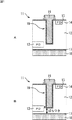
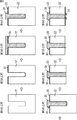
図1を参照して、従来の縦型トランジスタの構造について説明する。図1は、縦型トランジスタが形成された固体撮像素子の構成例を示す断面図であり、図1の上側が、固体撮像素子の表面側とされ、図1の下側が固体撮像素子の裏面側とされる。 The structure of a conventional vertical transistor will be described with reference to FIG. FIG. 1 is a cross-sectional view illustrating a configuration example of a solid-state imaging device in which a vertical transistor is formed. The upper side of FIG. 1 is the front side of the solid-state imaging device, and the lower side of FIG. It is said.
図1Aに示すように、固体撮像素子11では、半導体基板12の深い位置にPD(Photodiode:フォトダイオード)13が配置されるとともに、半導体基板12の表面側にFD(Floating diffusion:フローティングディフュージョン)14が配置されている。そして、半導体基板12の表面と、半導体基板12の表面側から形成されたトレンチとにゲート絶縁膜15が形成されており、そのトレンチにゲート電極16が埋め込まれている。また、半導体基板12の裏面側には、反射防止膜17および酸化膜18が積層されている。
As shown in FIG. 1A, in the solid-
このような固体撮像素子11では、ゲート電極16に電圧を印加することで、光電変換によりPD13に蓄積された電荷がFD14に転送される構造で縦型トランジスタ19が構成されている。
In such a solid-
ところで、縦型トランジスタ19の製造工程において、半導体基板12にトレンチを形成する際にトレンチの深さを制御することは困難であり、トレンチの深さが画素ごとにばらつくことがあった。これにより、図1Bに示すように、縦型トランジスタ19を構成するゲート電極16と、半導体基板12の裏面との間隔がばらつくことになり、このばらつきが画素特性に悪影響を与えることがあった。
By the way, in the manufacturing process of the
即ち、縦型トランジスタ19と半導体基板12の裏面の間隔のばらつきは、縦型トランジスタ19を加工する際のドライエッチング工程での深さ制御のばらつきや、半導体基板12自体の膜厚ばらつきに起因する。さらに、半導体基板12の膜厚ばらつきは、裏面照射型半導体製造プロセスにおける半導体基板薄肉化プロセスにおいて強調されてしまう。また、縦型トランジスタ19と、半導体基板12の裏面との間隔のばらつきは、半導体基板12の表面側から深い位置にあるPD13と縦型トランジスタ19の底部との間隔、もしくは被り量のばらつきとも言える。PD13と縦型トランジスタ19の底部との間隔は、光電変換された電荷の転送効率に大きく影響を与えるため、ばらつきを可能な限り抑える必要がある。
That is, the variation in the distance between the
このため、半導体基板12の裏面から光を照射する裏面照射型の撮像素子では、ゲート電極16を半導体基板12の裏面まで貫通させて縦型トランジスタ19を構成する構造である貫通縦型トランジスタ構造を採用することが有用である。
For this reason, in a back-illuminated imaging device that irradiates light from the back surface of the
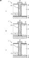
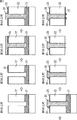
次に、図2を参照して、貫通縦型トランジスタ構造について説明する。図2は、貫通縦型トランジスタ構造の固体撮像素子の構成例を示す断面図であり、図2の上側が、固体撮像素子の表面側とされ、図2の下側が固体撮像素子の裏面側とされる。 Next, the through vertical transistor structure will be described with reference to FIG. FIG. 2 is a cross-sectional view illustrating a configuration example of a solid-state imaging device having a penetrating vertical transistor structure. The upper side of FIG. 2 is the front side of the solid-state imaging device, and the lower side of FIG. Is done.
図2Aに示すように、貫通縦型トランジスタ構造の固体撮像素子11’では、半導体基板12の裏面まで貫通するように形成されたトレンチにゲート電極16’が埋め込まれることで貫通縦型トランジスタ19’が構成されている。このような構成により、貫通縦型トランジスタ19’では、ゲート電極16’の深さは画素ごとに同一となり、上述したようなばらつきは解消される。
As shown in FIG. 2A, in a solid-
しかしながら、固体撮像素子11’では、トレンチが貫通しているため、ゲート絶縁膜15’がゲート電極16’の先端面側には形成されない構造となり、ゲート電極16’の先端面が反射防止膜17に接触する構成となる。これにより、図2Bに示すように、貫通縦型トランジスタ構造の固体撮像素子11’では、貫通縦型トランジスタ19’の先端部分において、反射防止膜17を介して半導体基板12とゲート電極16’との間で電流(ゲートリーク電流)が流れる恐れがあった。
However, in the solid-
特に、図2Cに示すように、製造工程において、貫通縦型トランジスタ19’の先端部分のゲート絶縁膜15’が後退し、半導体基板12とゲート電極16’との間に挟まれるように、半導体基板12の裏面側に成膜される反射防止膜17が形成されることがある。この場合、半導体基板12とゲート電極16’との間でゲートリーク電流がさらに流れ易くなる。また、半導体基板12とゲート電極16’との間に酸化膜18が形成されてしまう場合も同様にゲートリーク電流が流れ易くなる。
In particular, as shown in FIG. 2C, in the manufacturing process, the
このようなゲートリーク電流の発生は、裏面側で成膜する反射防止膜17および酸化膜18の膜質の悪さに起因する。即ち、裏面側で成膜する材料は、金属配線層やウェハ接合面の接着剤の耐熱温度に律速されてしまい高温成膜することができないため、膜質が悪くなり、表面工程で作成する絶縁膜と比較して電流が流れ易い。このことにより、半導体基板12とゲート電極16’との間の電界の加わる領域やその近くに反射防止膜17や酸化膜18を形成すると、半導体基板12とゲート電極16’との間にゲートリーク電流が発生することになる。
The generation of such a gate leakage current is caused by poor film quality of the
上述したように、従来の貫通縦型トランジスタの構成では、半導体基板とゲート電極との間でゲートリーク電流が発生する。これにより、貫通縦型トランジスタの先端部分にキャリアが大量に発生してしまい、電荷蓄積時や電荷転送時にキャリアがフォトダイオードに流れ込むことで、白点または暗電流が発生するなど、画素特性が低下することがあった。 As described above, in the configuration of the conventional through vertical transistor, a gate leakage current is generated between the semiconductor substrate and the gate electrode. As a result, a large amount of carriers are generated at the tip of the through-type vertical transistor, and the carrier characteristics flow into the photodiode during charge accumulation or charge transfer, resulting in white dots or dark current, resulting in poor pixel characteristics. There was something to do.
本発明は、このような状況に鑑みてなされたものであり、より良好な画素特性を備えることができるようにするものである。 The present invention has been made in view of such a situation, and makes it possible to provide better pixel characteristics.
本発明の一側面の固体撮像素子は、半導体で構成され、互いに反対側を向く第1および第2の面を有する基板と、前記第1の面と前記第2の面とを貫通するように前記基板に対して形成されたトレンチに成膜されたゲート絶縁膜と、前記ゲート絶縁膜を介して前記トレンチ内に、前記基板の前記第2の面側に露出するように埋め込まれたゲート電極とを備え、前記基板の前記第2の面から、前記ゲート電極の前記第2の面側の先端面までの間に段差が形成されている。 A solid-state imaging device according to one aspect of the present invention is configured by a semiconductor and has a substrate having first and second surfaces facing opposite sides, and the first surface and the second surface. A gate insulating film formed in a trench formed for the substrate, and a gate electrode embedded in the trench through the gate insulating film so as to be exposed on the second surface side of the substrate And a step is formed between the second surface of the substrate and the tip surface of the gate electrode on the second surface side.
本発明の一側面の電子機器は、半導体で構成され、互いに反対側を向く第1および第2の面を有する基板と、前記第1の面と前記第2の面とを貫通するように前記基板に対して形成されたトレンチに成膜されたゲート絶縁膜と、前記ゲート絶縁膜を介して前記トレンチ内に、前記基板の前記第2の面側に露出するように埋め込まれたゲート電極とを有し、前記基板の前記第2の面から、前記ゲート電極の前記第2の面側の先端面までの間に段差が形成されている固体撮像素子を備える。 According to another aspect of the invention, there is provided an electronic apparatus that includes a semiconductor and includes a substrate having first and second surfaces facing opposite sides, and the first surface and the second surface. A gate insulating film formed in a trench formed with respect to the substrate; and a gate electrode embedded in the trench through the gate insulating film so as to be exposed on the second surface side of the substrate; And a solid-state imaging device in which a step is formed from the second surface of the substrate to a tip surface on the second surface side of the gate electrode.
本発明の一側面の固体撮像素子の製造方法は、半導体で構成され、互いに反対側を向く第1および第2の面を有する基板の前記第1の面と前記第2の面とを貫通するように前記基板に対して形成されたトレンチに、ゲート絶縁膜を成膜し、前記ゲート絶縁膜を介して前記トレンチ内に、前記基板の前記第2の面側に露出するようにゲート電極を埋め込み、前記基板の前記第2の面から、前記ゲート電極の前記第2の面側の先端面までの間に段差を形成するステップを含む。 According to another aspect of the present invention, there is provided a method of manufacturing a solid-state imaging device, which is formed of a semiconductor and penetrates the first surface and the second surface of a substrate having first and second surfaces facing opposite to each other. A gate insulating film is formed in the trench formed with respect to the substrate, and a gate electrode is exposed to the second surface side of the substrate in the trench through the gate insulating film. Embedding and forming a step between the second surface of the substrate and the tip surface of the gate electrode on the second surface side.
本発明の一側面においては、半導体で構成され、互いに反対側を向く第1および第2の面を有する基板の第1の面と第2の面とを貫通するように基板に対して形成されたトレンチにゲート絶縁膜が成膜される。また、ゲート絶縁膜を介してトレンチ内に、基板の第2の面側に露出するようにゲート電極が埋め込まれる。そして、基板の第2の面から、ゲート電極の第2の面側の先端面までの間に段差が形成されている。 In one aspect of the present invention, the semiconductor substrate is formed with respect to the substrate so as to penetrate the first surface and the second surface of the substrate having first and second surfaces facing each other. A gate insulating film is formed in the trench. A gate electrode is embedded in the trench through the gate insulating film so as to be exposed on the second surface side of the substrate. A step is formed between the second surface of the substrate and the tip surface on the second surface side of the gate electrode.
本発明の一側面によれば、より良好な画素特性を備えることができる。 According to one aspect of the present invention, better pixel characteristics can be provided.
以下、本発明を適用した具体的な実施の形態について、図面を参照しながら詳細に説明する。 Hereinafter, specific embodiments to which the present invention is applied will be described in detail with reference to the drawings.
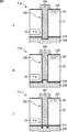
図3は、本発明を適用した固体撮像素子の第1乃至第3の実施の形態の構成例を示す断面図である。 FIG. 3 is a cross-sectional view showing a configuration example of the first to third embodiments of the solid-state imaging device to which the present invention is applied.
図3Aには、第1の実施の形態である固体撮像素子21Aが示されており、図3Bには、第2の実施の形態である固体撮像素子21Bが示されており、図3Cには、第3の実施の形態である固体撮像素子21Cが示されている。また、図3の上側が、固体撮像素子の表面側とされ、図3の下側が固体撮像素子の裏面側とされる。
3A shows a solid-
図3Aに示すように、固体撮像素子21Aは、半導体基板22、PD23、FD24、ゲート絶縁膜25A、ゲート電極26A、反射防止膜27A、酸化膜28Aを有して構成される。また、固体撮像素子21Aでは、光電変換によりPD23に蓄積された電荷が、ゲート電極26Aに電圧を印加することでFD24に転送される構造で貫通縦型トランジスタ29Aが構成されている。
As shown in FIG. 3A, the solid-
また、固体撮像素子21Aにおいて、半導体基板22は、例えば、半導体で構成された薄いシリコン製の基板であり、図3において、上側が半導体基板22の表面側(第1の面側)とされ、下側が半導体基板22の裏面側(第2の面側)とされる。PD23は、固体撮像素子21Aの面方向に沿って配置される複数の画素ごとに設けられ、半導体基板22の表面側から見て深い位置に配置され、固体撮像素子21Aの裏面側から照射される光により光電変換を行う。FD24は、半導体基板22の表面側に形成され、FD24には、PD23で光電変換されて蓄積されていた電荷が転送される。
In the solid-
ゲート絶縁膜25Aは、半導体基板22とゲート電極26Aとの間を絶縁するための膜であり、ゲート電極26Aは、PD23からFD24への電荷の転送を制御する電極である。また、反射防止膜27Aは、固体撮像素子21Aに照射された光の反射を軽減して、半導体基板22内への光の透過率を増加させるための膜であり、酸化膜28Aは、半導体基板22の裏面側を絶縁するための膜である。
The
そして、固体撮像素子21Aでは、図2に示した固体撮像素子11’と異なり、ゲート絶縁膜25Aおよびゲート電極26Aが半導体基板22の裏面側の面よりも突出するように、貫通縦型トランジスタ29Aの裏面側の先端部分が構成されている。
In the solid-
このように、ゲート絶縁膜25Aおよびゲート電極26Aが半導体基板22の裏面側の面よりも突出するように段差を有する構成のため、半導体基板22の裏面に成膜される反射防止膜27Aは、固体撮像素子21Aの裏面に対して凸形状となるように成膜される。つまり、反射防止膜27Aは、半導体基板22の裏面と、ゲート絶縁膜25Aおよびゲート電極26Aの裏面側の先端面とに成膜されるとともに、ゲート絶縁膜25Aの外周面に沿って成膜される。
Thus, since the
従って、固体撮像素子21Aにおいては、図2に示した固体撮像素子11’においてゲートリーク電流が流れるリーク経路よりも、ゲート絶縁膜25Aの外周面に沿って反射防止膜27Aが成膜される分に応じてリーク経路が長くなる。これにより、固体撮像素子21Aでは、半導体基板22とゲート電極26Aとの間におけるリーク電流の発生を抑制することができる。
Therefore, in the solid-
さらに、図2Cを参照して説明したように、固体撮像素子11’では、半導体基板12とゲート電極16’との間に挟み込まれるように反射防止膜17が形成されたときには、ゲートリーク電流が流れ易くなっていた。これに対し、固体撮像素子21Aでは、ゲート絶縁膜25Aおよびゲート電極26Aが半導体基板22の裏面側の面よりも突き出すように貫通縦型トランジスタ29Aが構成されている。この構成により、固体撮像素子21Aの製造工程において、半導体基板22とゲート電極26Aとの間に反射防止膜27Aなどが挟み込まれることはなく、固体撮像素子21Aでは、ゲートリーク電流の発生をより確実に抑制することができる。
Furthermore, as described with reference to FIG. 2C, in the solid-
また、図3Bに示すように、固体撮像素子21Bは、半導体基板22、PD23、FD24、ゲート絶縁膜25B、ゲート電極26B、反射防止膜27B、酸化膜28Bを有して構成される。また、固体撮像素子21Bでは、ゲート電極26Bが半導体基板22の裏面側まで貫通しており、貫通縦型トランジスタ29Bが構成されている。なお、以下では、固体撮像素子21Aと共通する部分についての説明は省略する。
As shown in FIG. 3B, the solid-
固体撮像素子21Bにおいて、貫通縦型トランジスタ29Bの裏面側の先端部分は、ゲート絶縁膜25Bが半導体基板22の裏面側の面まで形成されるとともに、ゲート電極26Bが半導体基板22の裏面側の面よりも凹む(窪む)ように段差を有する構成となっている。つまり、固体撮像素子21Bでは、ゲート電極26Bよりもゲート絶縁膜25Bが裏面側に延在するように形成される。
In the solid-
このような構成により、固体撮像素子21Bでは、半導体基板22の裏面に成膜される反射防止膜27Bが、固体撮像素子21Bの裏面に対して凹形状となるように成膜される。つまり、反射防止膜27Bは、半導体基板22の裏面およびゲート電極26Bの裏面側の先端面と、ゲート電極26Bの裏面側の先端面とに成膜されるとともに、ゲート絶縁膜25Bの内周面に沿って成膜される。
With such a configuration, in the solid-
従って、固体撮像素子21Bにおいては、固体撮像素子21Aと同様に、ゲート絶縁膜25Bの内周面に沿って反射防止膜27Bが成膜される分に応じてリーク経路が長くなる。これにより、固体撮像素子21Bでは、半導体基板22とゲート電極26Bとの間でのゲートリーク電流の発生を抑制することができる。また、固体撮像素子21Bの製造工程において、半導体基板22とゲート電極26Bとの間に反射防止膜27Bなどが挟み込まれることはなく、固体撮像素子21Bでは、ゲートリーク電流の発生をより確実に抑制することができる。
Therefore, in the solid-
また、図3Cに示すように、固体撮像素子21Cは、半導体基板22、PD23、FD24、ゲート絶縁膜25C、ゲート電極26C、反射防止膜27C、酸化膜28Cを有して構成される。また、固体撮像素子21Cでは、ゲート電極26Cが半導体基板22の裏面側まで貫通しており、貫通縦型トランジスタ29Cが構成されている。なお、以下では、固体撮像素子21Aと共通する部分についての説明は省略する。
As shown in FIG. 3C, the solid-state imaging device 21C includes a
固体撮像素子21Cにおいて、貫通縦型トランジスタ29Cの裏面側の先端部分は、ゲート電極26Cが半導体基板22の裏面側の面まで形成されるとともに、ゲート絶縁膜25Cが半導体基板22の裏面側の面よりも突出するように段差を有する構成となっている。つまり、固体撮像素子21Cでは、ゲート絶縁膜25Cが、半導体基板22およびゲート電極26Cの裏面側の面よりも突出するように形成されている。
In the solid-state imaging device 21C, the back end side portion of the through-type vertical transistor 29C has a gate electrode 26C formed up to the surface on the back surface side of the
このような構成により、固体撮像素子21Cでは、半導体基板22の裏面に成膜される反射防止膜27Cが、ゲート絶縁膜25Cに沿って円環状に凸形状となるように成膜される。つまり、反射防止膜27Cは、半導体基板22の裏面およびゲート電極26Cの裏面側の先端面と、ゲート電極26Cの裏面側の先端面とに成膜されるとともに、ゲート絶縁膜25Cの外周面および内周面に沿って成膜される。
With such a configuration, in the solid-state imaging device 21C, the antireflection film 27C formed on the back surface of the
従って、固体撮像素子21Cにおいては、ゲート絶縁膜25Cの外周面および内周面に沿って反射防止膜27Cが成膜される分に応じて、つまり固体撮像素子21Aおよび21Bの2倍程度、リーク経路が長くなる。これにより、固体撮像素子21Cでは、半導体基板22とゲート電極26Cとの間でのゲートリーク電流の発生を、固体撮像素子21Aおよび21Bよりもさらに抑制することができる。また、固体撮像素子21Cの製造工程において、半導体基板22とゲート電極26Cとの間に反射防止膜27Cなどが挟み込まれることはなく、固体撮像素子21Cでは、ゲートリーク電流の発生をより確実に抑制することができる。
Accordingly, in the solid-state image pickup device 21C, the antireflection film 27C is formed along the outer peripheral surface and the inner peripheral surface of the gate insulating film 25C, that is, about twice as much as the solid-state
さらに、固体撮像素子21Cでは、ゲート絶縁膜25Cが、半導体基板22およびゲート電極26Cの裏面側の面よりも突出するように形成されることにより、半導体基板22とゲート電極26Cとの間で電圧が直線状に印加されない構成となっている。つまり、固体撮像素子21Cでは、ゲート絶縁膜25Cが突出することにより、半導体基板22とゲート電極26Cとの間で直線的なリーク経路が発生しないように、反射防止膜27Cおよび酸化膜28Cが形成されている。このように、直線的なリーク経路が発生しない構成であるため、固体撮像素子21Cでは、固体撮像素子21Aまたは21Bよりも、ゲートリーク電流の発生を確実に抑制することができる。例えば、固体撮像素子21Aまたは21Bでは、ゲート絶縁膜25Aまたは25Bがミクロ的に後退してしまった場合には、直線的なリーク経路が発生する恐れがある。これに対し、固体撮像素子21Cでは、ゲート絶縁膜25Cが十分に突出しているため、直線的なリーク経路が発生することがなく、ゲートリーク電流の発生を確実に抑制することができる。
Furthermore, in the solid-state imaging device 21C, the gate insulating film 25C is formed so as to protrude from the back surface side of the
なお、以下適宜、ゲート絶縁膜25A乃至25C、ゲート電極26A乃至26C、反射防止膜27A乃至27C、酸化膜28A乃至28C、および貫通縦型トランジスタ29A乃至29Cについて、それぞれを区別する必要がない場合、ゲート絶縁膜25、ゲート電極26、反射防止膜27、酸化膜28、および貫通縦型トランジスタ29と称する。
In the following description, the
ここで、ゲート絶縁膜25、ゲート電極26、反射防止膜27、および酸化膜28を構成する素材について説明する。
Here, materials constituting the
ゲート絶縁膜25は、シリコンを熱酸化させた酸化シリコン膜、酸化窒化シリコン、または、高誘電体絶縁膜である。高誘電体絶縁膜としては、酸化ハフニウムや、ハフニアシリケート、窒素添加ハフニウムアルミネート、酸化タンタル、二酸化チタン、酸化ジルコニウム、酸化プラセオジム、酸化イットリウムなどが使用される。
The
ゲート電極26は、PDAS(Phosphorus Doped Amorphous Silicon)などのドープされたシリコン材料、または、アルミニウムや、タングステン、チタン、コバルト、ハフニウム、タンタルなどの金属材料により構成される。
The
反射防止膜27は、アルミニウム、タンタル、ハフニウム、チタン、ランタンなどの酸化物絶縁膜であり、他の負の固定電荷を有する絶縁膜を用いることもできる。負の固定電荷を有する絶縁膜には、酸化ハフニウム、酸化タンタル、酸化アルミニウム、酸化ジルコニウム、もしくは酸化チタンを用いることができる。
The
酸化膜28は、HDP(High Density Plasma)酸化膜などの堆積酸化膜である。
The
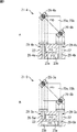
次に、図4および図5を参照して、貫通縦型トランジスタ29を備えた固体撮像素子の変形例について説明する。また、図4および図5では、固体撮像素子の平面図が上側に示されており、平面図に示されている一点鎖線における断面図が下側に示されている。なお、図4および図5では、FD24、ゲート絶縁膜25、反射防止膜27、および酸化膜28の図示は省略されている。
Next, with reference to FIG. 4 and FIG. 5, a modified example of the solid-state imaging device including the through vertical transistor 29 will be described. 4 and 5, the plan view of the solid-state imaging device is shown on the upper side, and the cross-sectional view taken along the alternate long and short dash line shown in the plan view is shown on the lower side. 4 and 5, the
図4Aには、第1の変形例である固体撮像素子21−1が示されている。固体撮像素子21−1では、ゲート電極26−1が円柱形状で形成されている。 FIG. 4A shows a solid-state imaging device 21-1 as a first modification. In the solid-state imaging device 21-1, the gate electrode 26-1 is formed in a cylindrical shape.
図4Bには、第2の変形例である固体撮像素子21−2が示されている。固体撮像素子21−2では、ゲート電極26−2がPD23の一辺に沿って細長い角柱形状で形成されている。つまり、固体撮像素子21−2では、PD23から電荷を転送する際の転送ゲート面積が広くなるように、ゲート電極26−2が形成されている。これにより、電荷の転送効率を向上させることができる。
FIG. 4B shows a solid-state imaging device 21-2 as a second modification. In the solid-state imaging device 21-2, the gate electrode 26-2 is formed in an elongated prismatic shape along one side of the
図4Cには、第3の変形例である固体撮像素子21−3が示されている。固体撮像素子21−3では、ゲート電極26−3がPD23の外周を囲うように、平面的に見てロ字形状で形成されている。つまり、PD23は画素ごとに設けられており、固体撮像素子21−3においては、ゲート電極26−3が、PD23を囲うように形成されることで、画素を分離させる機能を備える。さらに、固体撮像素子21−3では、PD23から電荷を転送する際の転送ゲート面積が広くなるので、電荷の転送効率を向上させることができる。
FIG. 4C shows a solid-state imaging device 21-3 as a third modification. In the solid-state imaging device 21-3, the gate electrode 26-3 is formed in a square shape as viewed in plan so as to surround the outer periphery of the
図5Aには、第4の変形例である固体撮像素子21−4が示されている。固体撮像素子21−4では、2つのPD23aおよび23bが異なる深さで半導体基板22内に配置されている。そして、固体撮像素子21−4では、PD23aの電荷を転送する貫通縦型トランジスタ29−4aを構成するゲート電極26−4a、および、PD23bの電荷を転送する貫通縦型トランジスタ29−4bを構成するゲート電極26−4bが設けられている。
FIG. 5A shows a solid-state imaging device 21-4 as a fourth modification. In the solid-state imaging device 21-4, the two PDs 23a and 23b are disposed in the
図5Bには、第5の変形例である固体撮像素子21−5が示されている。固体撮像素子21−5では、2つのPD23aおよび23bが異なる深さで半導体基板22内に配置されている。そして、固体撮像素子21−5では、PD23aの電荷を転送する縦型トランジスタ29−5aを構成するゲート電極26−5a、および、PD23bの電荷を転送する貫通縦型トランジスタ29−5bを構成するゲート電極26−5bが設けられている。
FIG. 5B shows a solid-state imaging device 21-5 that is a fifth modification. In the solid-state imaging device 21-5, the two PDs 23a and 23b are arranged in the
このように、固体撮像素子21では、複数(図5の例では2つ)のPD23を、単一画素内において、半導体基板22に入射する光の光吸収係数の波長依存性に対応した深さに配置することができる。そして、それぞれのPD23に対応して複数の貫通縦型トランジスタ29が設けられる。
As described above, in the solid-state imaging device 21, a plurality of (two in the example of FIG. 5) PDs 23 have a depth corresponding to the wavelength dependency of the light absorption coefficient of light incident on the
このとき、複数の貫通縦型トランジスタ29のうちの少なくとも一部が、図3を参照して説明したように、半導体基板22の裏面側の面から突出した構成となっていればよい。つまり、図5Aの固体撮像素子21−4では、貫通縦型トランジスタ29−4aおよび29−4bの両方とも先端部分が半導体基板22の裏面側の面から突出している。これに対し、図5Bの固体撮像素子21−5では、貫通縦型トランジスタ29−5aの先端部分だけが半導体基板22の裏面側の面から突出している。このように、固体撮像素子21では、PD23の構成などに応じて、貫通縦型トランジスタ29の深さを適宜調整することができる。
At this time, it is only necessary that at least a part of the plurality of through vertical transistors 29 protrude from the rear surface of the
なお、図4および図5に示した固体撮像素子21の変形例には、ゲート電極26が半導体基板22の裏面側の面から突出する構造、即ち、図3Aに示した貫通縦型トランジスタ29Aの構造が示されているが、これに限られるものではない。つまり、固体撮像素子21の変形例それぞれに対して、貫通縦型トランジスタ29Bまたは29Cの構造をそれぞれ適用することができる。
In the modification of the solid-state imaging device 21 shown in FIGS. 4 and 5, the
次に、図6を参照して、固体撮像素子21の製造工程について説明する。 Next, a manufacturing process of the solid-state imaging device 21 will be described with reference to FIG.
第1の工程では、第1導電型である、例えば、p型の半導体基板22に、貫通縦型トランジスタ29を形成するためのトレンチが形成される。なお、図示しないが、半導体基板22にトレンチを形成する工程の前に、PD23が形成されている。PD23は、半導体基板22に入射する光の光吸収係数の波長依存性に対応した深さに、第2導電型であるn型の半導体領域と第1導電型であるp型の半導体領域とを、イオン注入法によって交互に複数積層することにより形成される。また、それぞれの画素は、第1導電型である半導体基板22によって分離される。
In the first step, a trench for forming the through vertical transistor 29 is formed in the first conductivity type, for example, a p-
第2の工程では、半導体基板22の表面と、第1の工程で形成されたトレンチの内部にゲート絶縁膜25が形成される。例えば、ゲート絶縁膜25は、シリコンを熱酸化させた酸化シリコン膜、酸化窒化シリコン、高誘電体絶縁膜である。また、高誘電体絶縁膜としては、酸化ハフニウム、ハフニアシリケート、窒素添加ハフニウムアルミネート、酸化タンタル、二酸化チタン、酸化ジルコニウム、酸化プラセオジム、酸化イットリウムなどである。
In the second step, the
第3の工程では、トレンチの内部にゲート絶縁膜25を介してゲート電極26となる材料が埋め込まれる。ここで、ゲート電極26となる材料としては、PDAS(Phosphorus Doped Amorphous Silicon)などのドープされたシリコン材料、または、アルミニウムや、タングステン、チタン、コバルト、ハフニウム、タンタルなどの金属材料が用いられる。
In the third step, a material that becomes the
第4の工程では、ゲート電極26を形成する領域に対応したレジストマスク(図示せず)が形成され、このレジストをマスクとして異方性エッチングによりゲート電極26が加工される。その後、ゲート電極26と半導体基板22の界面準位を終端するため、塩素雰囲気中でアニール処理が施される。
In the fourth step, a resist mask (not shown) corresponding to a region for forming the
第5の工程では、半導体基板22の表面に酸化膜や窒化膜などが堆積されて、その後に等方性エッチングが行われることで、サイドウォール30が形成される。なお、サイドウォール30の形成後、通常の固体撮像素子と同様に、半導体基板22の表面側に層間絶縁膜を伴った複数の配線層(図示せず)が形成される。さらに、半導体基板22の表面側の最上層に、半導体基板22を支持する半導体基板(図示せず)が接合される。
In the fifth step, an oxide film, a nitride film, or the like is deposited on the surface of the
第6の工程では、例えば、半導体基板22の裏面側を研磨することで、ゲート電極26の裏面側の先端部分が、半導体基板22の裏面側の面に露出する所望の膜厚となるような薄膜加工が行われる。例えば、半導体基板22の厚みは、0.1μm〜100μm程度、より好ましくは、1μm〜10μm程度とされる。
In the sixth step, for example, by polishing the back surface side of the
第7の工程では、半導体基板22およびゲート電極26をエッチバックさせる溶液、例えば、水酸化アンモニウムと過酸化水素水の水溶液であるSC1溶液により、半導体基板22の裏面側の面、および、ゲート電極26の裏面側の先端面を後退させる。このように、半導体基板22の裏面側の面、および、ゲート電極26の裏面側の先端面が後退することで、ゲート絶縁膜25が突出することになる。ここで、ゲート絶縁膜25は、例えば、0.1nmから300nm程度で突出される。なお、ゲート絶縁膜25を突出させる処理は、CMP(Chemical Mechanical Polishing)により行ってもよい。
In the seventh step, a solution for etching back the
第8の工程では、反射防止膜27が半導体基板22の裏面側に堆積される。また、反射防止膜27を成膜した後、酸化膜28(図3)が堆積される。反射防止膜27は、アルミニウム、タンタル、ハフニウム、チタン、ランタンなどの酸化物絶縁膜であり、反射防止膜27には、他の負の固定電荷を有する絶縁膜を用いることもできる。負の固定電荷を有する絶縁膜には、酸化ハフニウム、酸化タンタル、酸化アルミニウム、酸化ジルコニウム、もしくは酸化チタンを用いることができる。なお、反射防止膜27は、例えば、ALD(Atomic Layer Deposition)で成膜した後、HDP(High Density Plasma)で膜厚を厚くしてもよい。
In the eighth step, an
さらに、第8の工程の後、半導体基板22の内部に光を照射させない領域に遮光膜(図示せず)が堆積される。遮光膜は、例えば、タングステンや、チタン、アルミニウムなどにより形成される。さらに、平坦化膜、カラーフィルタおよびオンチップマイクロレンズ(それぞれ図示せず)が順次形成される。
Further, after the eighth step, a light shielding film (not shown) is deposited in a region where light is not irradiated inside the
このような製造工程により、図3Cに示したような、ゲート絶縁膜25Cが半導体基板22の裏面側の面よりも突出して形成された構造の貫通縦型トランジスタ29Cを形成することができる。
Through such a manufacturing process, the through vertical transistor 29C having a structure in which the gate insulating film 25C is formed so as to protrude from the back surface of the
次に、図7を参照して、固体撮像素子21の他の製造工程について説明する。なお、この製造工程は、半導体基板22として、SOI(Silicon On Insulator)基板を用いる点において、図6で説明した製造工程と異なっている。
Next, another manufacturing process of the solid-state imaging device 21 will be described with reference to FIG. This manufacturing process is different from the manufacturing process described with reference to FIG. 6 in that an SOI (Silicon On Insulator) substrate is used as the
第1の工程では、第1導電型である、例えば、p型の半導体基板22に、貫通縦型トランジスタ29を形成するためのトレンチが形成される。このとき、トレンチは、SOI基板のBOX層31まで到達するように加工される。なお、トレンチを形成するために半導体基板22の表面に形成されたマスクを除去する際に、トレンチの先端側に存在するBOX層31の一部が後退する。これにより、図7に示すように、トレンチの先端側においてBOX層31の一部に空間が形成される。
In the first step, a trench for forming the through vertical transistor 29 is formed in the first conductivity type, for example, a p-
なお、図示しないが、半導体基板22にトレンチを形成する工程の前に、PD23が形成されている。PD23は、半導体基板22に入射する光の光吸収係数の波長依存性に対応した深さに、第2導電型であるn型の半導体領域と第1導電型であるp型の半導体領域とを、イオン注入法によって交互に複数積層することにより形成される。また、それぞれの画素は、第1導電型である半導体基板22によって分離される。
Although not shown, the
その後、第2乃至第5の工程が行われる。なお、第2乃至第5の工程は、図6で説明した第2乃至第5の工程と同様であり、その説明は省略する。 Thereafter, the second to fifth steps are performed. The second to fifth steps are the same as the second to fifth steps described with reference to FIG.
そして、第6の工程では、半導体基板22に対して薄膜加工が行われる。この薄膜加工は、半導体基板22のBOX層31よりも裏面側(図7の下側)にある半導体基板を研磨により除去した後、BOX層31を、ウェットエッチングまたはドライエッチングにより除去することにより行われる。なお、BOX層31の除去にCMP(Chemical Mechanical Polishing)を用いてもよく、これらの加工方法を組み合わせて用いてもよい。
In the sixth step, thin film processing is performed on the
その後、第7および第8の工程が行われる。なお、第7および第8の工程は、図6で説明した第7および第8の工程と同様であり、その説明は省略する。 Thereafter, the seventh and eighth steps are performed. The seventh and eighth steps are the same as the seventh and eighth steps described with reference to FIG.
以上のような工程により、貫通縦型トランジスタ29を有する固体撮像素子21が製造される。そして、貫通縦型トランジスタ29の先端部分において、半導体基板22の裏面側の面からゲート電極26の裏面側の先端面までの間に段差が形成されることになる。つまり、図3Aの固体撮像素子21Aの構成では、ゲート絶縁膜25Aおよびゲート電極26Aが半導体基板22の裏面側の面よりも突出することにより段差が形成される。また、図3Bの固体撮像素子21Bの構成では、ゲート絶縁膜25Bが半導体基板22の裏面側の面まで形成されるとともに、ゲート電極26Bが半導体基板22の裏面側の面よりも凹むように形成されることにより段差が形成される。また、図3Cの固体撮像素子21Cの構成では、ゲート電極26Cが半導体基板22の裏面側の面まで形成されるとともに、ゲート絶縁膜25Cが半導体基板22の裏面側の面よりも突出するように形成されることにより段差が形成される。
The solid-state imaging device 21 having the through vertical transistor 29 is manufactured through the processes as described above. Then, a step is formed between the back surface side surface of the
このような段差が形成されることにより、半導体基板22とゲート電極26との間の電界が強い領域と、反射防止膜27や酸化膜28などの裏面工程で成膜される膜との間に段差に応じた間隔が設けられることになる。さらに、この製造工程では、半導体基板22とゲート電極26との間に反射防止膜27などが挟み込まれることは回避される。従って、固体撮像素子21では、ゲートリーク電流の発生を抑制することができる。
By forming such a step, there is a gap between the region where the electric field between the
また、このような構成の貫通縦型トランジスタ29を適用した固体撮像素子21は、ゲートリーク電流に起因した白点または暗電流が発生することはなく、安定した画素特性を得ることができる。また、プロセスばらつきに対するマージンが向上し、画素どうしの特性にばらつきが発生することもない。従って、固体撮像素子21では、より良好な画像を得ることができる。 In addition, the solid-state imaging device 21 to which the through vertical transistor 29 having such a configuration is applied does not generate a white spot or a dark current due to a gate leakage current, and can obtain stable pixel characteristics. Further, the margin for process variation is improved, and variations in characteristics between pixels do not occur. Therefore, the solid-state image sensor 21 can obtain a better image.
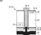
図8には、第6の変形例である固体撮像素子21−6が示されている。 FIG. 8 shows a solid-state imaging device 21-6 that is a sixth modification.
固体撮像素子21−6では、ゲート絶縁膜25−6が、半導体基板22およびゲート電極26−6の裏面側の面よりも突出して形成される構成となっている。そして、固体撮像素子21−6では、半導体基板22とゲート電極26−6との絶縁性を確保しながら、半導体基板22の裏面側に配設された金属材料32とゲート電極26−6とが接続される。
In the solid-state imaging device 21-6, the gate insulating film 25-6 is formed so as to protrude from the back surface of the
金属材料32は、ゲート電極26−6に電気的に接続される配線であり、ゲート電極26−6を介して金属材料32に電圧が印加されたり、金属材料32を介してゲート電極26−6に電圧が印加されたりする。例えば、固体撮像素子21−6では、金属材料32の裏面側に、さらに異種材料や構造が積層される構成が想定される。具体的には、金属材料32の裏面側に、光電変換膜を挟み込むように上部透明電極および下部透明電極が配置された構造が積層された構成において、ゲート電極26−6および金属材料32を介して、上部透明電極に電圧を印加するとともに下部透明電極の電圧を固定することで、光電変換膜で発生した電荷が基板に転送される。
The
また、金属材料32は、PD23に対応して開口するように形成され、半導体基板22に対して光を照射させない領域を遮光する遮光膜としての機能も備える。また、金属材料32は、アルミニウムや、タングステン、チタン、コバルト、ハフニウム、タンタル、各種のシリサイド材料などにより構成される。
Further, the
なお、遮光性の必要がない場合には、金属材料32に替えて、ゲート電極26−6に電気的に接続される配線として、透過性のある導電膜(図示せず)を採用してもよい。この透過性のある導電膜は、ITO (Indium-tin-oxide)や、ZnO,In2O3,SnO2,グラフェンなどにより構成される。
If light shielding is not necessary, a transmissive conductive film (not shown) may be employed as the wiring electrically connected to the gate electrode 26-6 instead of the
図9には、第7の変形例である固体撮像素子21−7と、その製造工程の一部が示されている。 FIG. 9 shows a solid-state imaging device 21-7 as a seventh modification and a part of the manufacturing process.
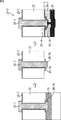
固体撮像素子21−7は、図7の製造工程で説明したSOI基板により製造される。図7を参照して説明したように、第1乃至第5の工程が行われて、図9の左側に示すように、半導体基板22に形成されたトレンチの内部にゲート電極26−7が埋め込まれる。このとき、上述したように、トレンチの先端側においてBOX層31の一部に空間が形成されており、その空間内にゲート電極26−7の先端部分26−7Aが充填されることになる。
The solid-state imaging device 21-7 is manufactured by the SOI substrate described in the manufacturing process of FIG. As described with reference to FIG. 7, the first to fifth steps are performed, and the gate electrode 26-7 is embedded in the trench formed in the
このような状態から薄膜加工を行うときに、ゲート電極26−7の裏面側の先端に形成された先端部分26−7Aが削除されずに、先端部分26−7Aが残るようにBOX層31が除去される。また、このとき、ゲート絶縁膜25−7の裏面側の先端においても、フランジ部25−7Aが形成されるようにBOX層31が除去される。
When performing thin film processing from such a state, the
そして、半導体基板22の裏面側に反射防止膜27−7が成膜され、酸化膜28−7が製膜される。その後、反射防止膜27−7および酸化膜28−7にゲート電極26−7まで貫通するような貫通穴が形成されて、ゲート電極26−7の先端部分26−7Aと接続するように金属材料32が配設される。
Then, an antireflection film 27-7 is formed on the back side of the
このように、ゲート電極26−7に形成された先端部分26−7Aを利用することで、裏面側から見たときに、ゲート電極26−7の面積よりも先端部分26−7Aの面積が広く、金属材料32を接続する際の配線作業を容易に行うことができる。
Thus, by using the tip portion 26-7A formed on the gate electrode 26-7, the area of the tip portion 26-7A is larger than the area of the gate electrode 26-7 when viewed from the back side. Wiring work when connecting the
また、上述したような固体撮像素子21は、例えば、デジタルスチルカメラやデジタルビデオカメラなどの撮像システム、撮像機能を備えた携帯電話機、または、撮像機能を備えた他の機器といった各種の電子機器に適用することができる。 The solid-state imaging device 21 as described above is used in various electronic devices such as an imaging system such as a digital still camera or a digital video camera, a mobile phone having an imaging function, or other devices having an imaging function. Can be applied.
図10は、電子機器に搭載される撮像装置の構成例を示すブロック図である。 FIG. 10 is a block diagram illustrating a configuration example of an imaging device mounted on an electronic device.
図10に示すように、撮像装置101は、光学系102、シャッタ装置103、撮像素子104、駆動回路105、信号処理回路106、モニタ107、およびメモリ108を備えて構成され、静止画像および動画像を撮像可能である。
As shown in FIG. 10, the
光学系102は、1枚または複数枚のレンズを有して構成され、被写体からの像光(入射光)を撮像素子104に導き、撮像素子104の受光面(センサ部)に結像させる。
The
シャッタ装置103は、光学系102および撮像素子104の間に配置され、駆動回路105の制御に従って、撮像素子104への光照射期間および遮光期間を制御する。
The
撮像素子104としては、上述したような実施の形態および変形例の固体撮像素子21のいずれかが適用される。撮像素子104には、光学系102およびシャッタ装置103を介して受光面に結像される像に応じて、一定期間、信号電荷が蓄積される。そして、撮像素子104に蓄積された信号電荷は、駆動回路105から供給される駆動信号(タイミング信号)に従って転送される。
As the
駆動回路105は、撮像素子104の転送動作、および、シャッタ装置103のシャッタ動作を制御する駆動信号を出力して、撮像素子104およびシャッタ装置103を駆動する。
The drive circuit 105 outputs a drive signal for controlling the transfer operation of the
信号処理回路106は、撮像素子104から出力された信号電荷に対して各種の信号処理を施す。信号処理回路106が信号処理を施すことにより得られた画像(画像データ)は、モニタ107に供給されて表示されたり、メモリ108に供給されて記憶(記録)されたりする。
The
このように構成されている撮像装置101では、撮像素子104として、上述したように画素特性が良好な固体撮像素子21を適用することにより、画質を向上させることができる。
In the
なお、上述した実施の形態では、固体撮像素子21として、裏面照射型のCMOS型固体撮像素子が採用された構成例を示しているが、固体撮像素子21の構造は、表面照射型のCMOS型固体撮像素子や、CCD型固体撮像素子などに適用することができる。 In the above-described embodiment, a configuration example in which a back-illuminated CMOS solid-state image sensor is employed as the solid-state image sensor 21 is shown. However, the structure of the solid-state image sensor 21 is a front-illuminated CMOS type. The present invention can be applied to a solid-state image sensor, a CCD solid-state image sensor, and the like.
また、本発明の実施の形態は、上述した実施の形態に限定されるものではなく、本発明の要旨を逸脱しない範囲において種々の変更が可能である。 The embodiments of the present invention are not limited to the above-described embodiments, and various modifications can be made without departing from the scope of the present invention.
21 固体撮像素子, 22 半導体基板, 23 PD, 24 FD, 25 ゲート絶縁膜, 26 ゲート電極, 27 反射防止膜, 28 酸化膜, 29 貫通縦型トランジスタ, 30 サイドウォール, 31 BOX層, 32 金属材料, 101 撮像装置, 102 光学系, 103 シャッタ装置, 104 撮像素子, 105 駆動回路, 106 信号処理回路, 107 モニタ, 108 メモリ 21 Solid-state imaging device, 22 Semiconductor substrate, 23 PD, 24 FD, 25 Gate insulating film, 26 Gate electrode, 27 Antireflection film, 28 Oxide film, 29 Through vertical transistor, 30 Side wall, 31 BOX layer, 32 Metal material , 101 imaging device, 102 optical system, 103 shutter device, 104 imaging device, 105 drive circuit, 106 signal processing circuit, 107 monitor, 108 memory
Claims (15)
前記第1の面と前記第2の面とを貫通するように前記基板に対して形成されたトレンチに成膜されたゲート絶縁膜と、
前記ゲート絶縁膜を介して前記トレンチ内に、前記基板の前記第2の面側に露出するように埋め込まれたゲート電極と
を備え、
前記基板の前記第2の面から、前記ゲート電極の前記第2の面側の先端面までの間に段差が形成されている
固体撮像素子。 A substrate made of a semiconductor and having first and second surfaces facing away from each other;
A gate insulating film formed in a trench formed in the substrate so as to penetrate the first surface and the second surface;
A gate electrode embedded in the trench through the gate insulating film so as to be exposed on the second surface side of the substrate;
A step is formed between the second surface of the substrate and a tip surface of the gate electrode on the second surface side.
請求項1に記載の固体撮像素子。 2. The solid-state imaging device according to claim 1, wherein the step is configured by projecting a front end surface on the second surface side of the gate electrode and the gate insulating film from the second surface of the substrate.
請求項1に記載の固体撮像素子。 2. The solid-state imaging device according to claim 1, wherein the step is formed by a tip surface on the second surface side of the gate electrode being recessed from the second surface of the substrate.
請求項1に記載の固体撮像素子。 2. The solid-state imaging device according to claim 1, wherein the step is configured by the gate insulating film projecting from the second surface of the substrate and a tip surface of the gate electrode on the second surface side. .
をさらに備え、
前記複数の画素ごとに、前記ゲート電極が前記フォトダイオードを囲うように形成される
請求項1に記載の固体撮像素子。 A photodiode provided for each of a plurality of pixels arranged in a surface direction along the first or second surface;
The solid-state imaging device according to claim 1, wherein the gate electrode is formed so as to surround the photodiode for each of the plurality of pixels.
をさらに備え、
前記ゲート電極は前記フォトダイオードごとに設けられ、それらの前記ゲート電極のうちの少なくとも1つの前記ゲート電極が、前記段差が形成される構成である
請求項1に記載の固体撮像素子。 A plurality of pixel units arranged in a plane direction along the first or second surface, further comprising photodiodes arranged at a plurality of locations having different depths in the substrate;
The solid-state imaging device according to claim 1, wherein the gate electrode is provided for each of the photodiodes, and at least one of the gate electrodes has a configuration in which the step is formed.
をさらに備える請求項1に記載の固体撮像素子。 The solid-state imaging device according to claim 1, further comprising: a wiring arranged on the second surface side of the substrate and connected to the gate electrode.
をさらに備える請求項1に記載の固体撮像素子。 The solid-state imaging device according to claim 1, further comprising an antireflection film in contact with the substrate on the second surface of the substrate.
請求項8に記載の固体撮像素子。 The solid-state imaging device according to claim 8, wherein the antireflection film is an oxide insulating film of silicon, aluminum, hafnium, tantalum, titanium, or lanthanum.
請求項1に記載の固体撮像素子。 The solid-state imaging device according to claim 1, wherein the gate insulating film is a silicon oxide film or silicon oxynitride.
請求項1に記載の固体撮像素子。 The solid-state imaging device according to claim 1, wherein the gate electrode is PDAS (Phosphorus Doped Amorphous Silicon), aluminum, tungsten, titanium, cobalt, hafnium, or tantalum.
請求項7に記載の固体撮像素子。 The solid-state imaging device according to claim 7, wherein the wiring is a metal material including aluminum, tungsten, titanium, cobalt, hafnium, tantalum, or a silicide material.
請求項7に記載の固体撮像素子。 The solid-state imaging device according to claim 7, wherein the wiring is ITO (Indium-tin-oxide), ZnO, In 2 O 3, SnO 2, or a conductive film including graphene and having transparency.
前記第1の面と前記第2の面とを貫通するように前記基板に対して形成されたトレンチに成膜されたゲート絶縁膜と、
前記ゲート絶縁膜を介して前記トレンチ内に、前記基板の前記第2の面側に露出するように埋め込まれたゲート電極と
を有し、前記基板の前記第2の面から、前記ゲート電極の前記第2の面側の先端面までの間に段差が形成されている固体撮像素子
を備える電子機器。 A substrate made of a semiconductor and having first and second surfaces facing away from each other;
A gate insulating film formed in a trench formed in the substrate so as to penetrate the first surface and the second surface;
A gate electrode embedded in the trench through the gate insulating film so as to be exposed on the second surface side of the substrate, and from the second surface of the substrate, the gate electrode An electronic apparatus comprising: a solid-state imaging device in which a step is formed between the second surface side and the front end surface.
前記ゲート絶縁膜を介して前記トレンチ内に、前記基板の前記第2の面側に露出するようにゲート電極を埋め込み、
前記基板の前記第2の面から、前記ゲート電極の前記第2の面側の先端面までの間に段差を形成する
ステップを含む固体撮像素子の製造方法。 A gate is formed in a trench formed with respect to the substrate so as to penetrate the first surface and the second surface of the substrate made of a semiconductor and having first and second surfaces facing opposite to each other. Insulating film is formed,
A gate electrode is embedded in the trench through the gate insulating film so as to be exposed on the second surface side of the substrate,
A method of manufacturing a solid-state imaging device, including a step of forming a step between the second surface of the substrate and a tip surface on the second surface side of the gate electrode.
Priority Applications (3)
| Application Number | Priority Date | Filing Date | Title |
|---|---|---|---|
| JP2011038668A JP2012175067A (en) | 2011-02-24 | 2011-02-24 | Image pickup device, and manufacturing method therefor, and electronic apparatus |
| US13/358,258 US8916916B2 (en) | 2011-02-24 | 2012-01-25 | Imaging device, method of manufacturing the same, and electronic apparatus |
| CN2012100356318A CN102651375A (en) | 2011-02-24 | 2012-02-16 | Solid-state imaging device, method of manufacturing the same, and electronic apparatus |
Applications Claiming Priority (1)
| Application Number | Priority Date | Filing Date | Title |
|---|---|---|---|
| JP2011038668A JP2012175067A (en) | 2011-02-24 | 2011-02-24 | Image pickup device, and manufacturing method therefor, and electronic apparatus |
Publications (2)
| Publication Number | Publication Date |
|---|---|
| JP2012175067A true JP2012175067A (en) | 2012-09-10 |
| JP2012175067A5 JP2012175067A5 (en) | 2014-04-03 |
Family
ID=46693337
Family Applications (1)
| Application Number | Title | Priority Date | Filing Date |
|---|---|---|---|
| JP2011038668A Ceased JP2012175067A (en) | 2011-02-24 | 2011-02-24 | Image pickup device, and manufacturing method therefor, and electronic apparatus |
Country Status (3)
| Country | Link |
|---|---|
| US (1) | US8916916B2 (en) |
| JP (1) | JP2012175067A (en) |
| CN (1) | CN102651375A (en) |
Cited By (6)
| Publication number | Priority date | Publication date | Assignee | Title |
|---|---|---|---|---|
| JP2017055050A (en) * | 2015-09-11 | 2017-03-16 | 株式会社東芝 | Solid state image sensor and manufacturing method of solid state image sensor |
| JP2017509142A (en) * | 2014-01-10 | 2017-03-30 | ケーエルエー−テンカー コーポレイション | Antireflective layer for backside illuminated sensors |
| JP2019117931A (en) * | 2019-02-20 | 2019-07-18 | 株式会社東芝 | Solid state image sensor and manufacturing method of solid state image sensor |
| WO2020045142A1 (en) * | 2018-08-30 | 2020-03-05 | ソニーセミコンダクタソリューションズ株式会社 | Imaging device and electronic instrument |
| JP2021141262A (en) * | 2020-03-06 | 2021-09-16 | Gpixel Japan株式会社 | Pixel for solid-state imaging device |
| WO2023199642A1 (en) * | 2022-04-15 | 2023-10-19 | ソニーセミコンダクタソリューションズ株式会社 | Light detection device and electronic apparatus |
Families Citing this family (9)
| Publication number | Priority date | Publication date | Assignee | Title |
|---|---|---|---|---|
| FR2984607A1 (en) * | 2011-12-16 | 2013-06-21 | St Microelectronics Crolles 2 | CURED PHOTODIODE IMAGE SENSOR |
| US9496425B2 (en) | 2012-04-10 | 2016-11-15 | Kla-Tencor Corporation | Back-illuminated sensor with boron layer |
| US9613886B2 (en) * | 2013-08-29 | 2017-04-04 | Industrial Technology Research Institute | Optical coupling module |
| US11114489B2 (en) | 2018-06-18 | 2021-09-07 | Kla-Tencor Corporation | Back-illuminated sensor and a method of manufacturing a sensor |
| US11114491B2 (en) | 2018-12-12 | 2021-09-07 | Kla Corporation | Back-illuminated sensor and a method of manufacturing a sensor |
| FR3091787A1 (en) * | 2019-01-14 | 2020-07-17 | Commissariat A L'energie Atomique Et Aux Energies Alternatives | Rear-illuminated image sensor |
| US11848350B2 (en) | 2020-04-08 | 2023-12-19 | Kla Corporation | Back-illuminated sensor and a method of manufacturing a sensor using a silicon on insulator wafer |
| US11527563B2 (en) * | 2020-04-20 | 2022-12-13 | Taiwan Semiconductor Manufacturing Company Limited | Photodetector using a buried gate electrode for a transfer transistor and methods of manufacturing the same |
| WO2022210367A1 (en) * | 2021-03-29 | 2022-10-06 | ヌヴォトンテクノロジージャパン株式会社 | Semiconductor device, battery protectoin circuit, and power management circuit |
Citations (3)
| Publication number | Priority date | Publication date | Assignee | Title |
|---|---|---|---|---|
| WO2006019156A1 (en) * | 2004-08-20 | 2006-02-23 | Zycube Co., Ltd. | Method for manufacturing semiconductor device having three-dimensional multilayer structure |
| JP2008258316A (en) * | 2007-04-03 | 2008-10-23 | Sharp Corp | Solid-state imaging device and its manufacturing method, and electronic information equipment |
| JP2010114273A (en) * | 2008-11-06 | 2010-05-20 | Sony Corp | Solid-state imaging device and electronic apparatus |
Family Cites Families (10)
| Publication number | Priority date | Publication date | Assignee | Title |
|---|---|---|---|---|
| CN100487898C (en) * | 2001-11-05 | 2009-05-13 | 佐伊科比株式会社 | Solid-state image sensor and its production method |
| KR100467027B1 (en) * | 2003-01-07 | 2005-01-24 | 삼성전자주식회사 | Static random access memory having vertical transistors and method for fabricating the same |
| JP4839008B2 (en) | 2005-03-28 | 2011-12-14 | 富士フイルム株式会社 | Single-plate color solid-state image sensor |
| KR100790257B1 (en) * | 2006-12-27 | 2008-01-02 | 동부일렉트로닉스 주식회사 | Semiconductor device and method for the same |
| JP2009272480A (en) * | 2008-05-08 | 2009-11-19 | Nec Electronics Corp | Method of manufacturing semiconductor device |
| JP5365144B2 (en) | 2008-11-06 | 2013-12-11 | ソニー株式会社 | SOLID-STATE IMAGING DEVICE, ITS MANUFACTURING METHOD, AND ELECTRONIC DEVICE |
| EP2133918B1 (en) * | 2008-06-09 | 2015-01-28 | Sony Corporation | Solid-state imaging device, drive method thereof and electronic apparatus |
| JP5369505B2 (en) * | 2008-06-09 | 2013-12-18 | ソニー株式会社 | Solid-state imaging device and electronic apparatus |
| JP4862878B2 (en) * | 2008-10-30 | 2012-01-25 | ソニー株式会社 | Solid-state imaging device, manufacturing method thereof, and imaging device |
| TWI445166B (en) * | 2008-11-07 | 2014-07-11 | Sony Corp | Solid-state imaging device, method for manufacturing solid-state imaging device, and electronic apparatus |
-
2011
- 2011-02-24 JP JP2011038668A patent/JP2012175067A/en not_active Ceased
-
2012
- 2012-01-25 US US13/358,258 patent/US8916916B2/en not_active Expired - Fee Related
- 2012-02-16 CN CN2012100356318A patent/CN102651375A/en active Pending
Patent Citations (3)
| Publication number | Priority date | Publication date | Assignee | Title |
|---|---|---|---|---|
| WO2006019156A1 (en) * | 2004-08-20 | 2006-02-23 | Zycube Co., Ltd. | Method for manufacturing semiconductor device having three-dimensional multilayer structure |
| JP2008258316A (en) * | 2007-04-03 | 2008-10-23 | Sharp Corp | Solid-state imaging device and its manufacturing method, and electronic information equipment |
| JP2010114273A (en) * | 2008-11-06 | 2010-05-20 | Sony Corp | Solid-state imaging device and electronic apparatus |
Cited By (6)
| Publication number | Priority date | Publication date | Assignee | Title |
|---|---|---|---|---|
| JP2017509142A (en) * | 2014-01-10 | 2017-03-30 | ケーエルエー−テンカー コーポレイション | Antireflective layer for backside illuminated sensors |
| JP2017055050A (en) * | 2015-09-11 | 2017-03-16 | 株式会社東芝 | Solid state image sensor and manufacturing method of solid state image sensor |
| WO2020045142A1 (en) * | 2018-08-30 | 2020-03-05 | ソニーセミコンダクタソリューションズ株式会社 | Imaging device and electronic instrument |
| JP2019117931A (en) * | 2019-02-20 | 2019-07-18 | 株式会社東芝 | Solid state image sensor and manufacturing method of solid state image sensor |
| JP2021141262A (en) * | 2020-03-06 | 2021-09-16 | Gpixel Japan株式会社 | Pixel for solid-state imaging device |
| WO2023199642A1 (en) * | 2022-04-15 | 2023-10-19 | ソニーセミコンダクタソリューションズ株式会社 | Light detection device and electronic apparatus |
Also Published As
| Publication number | Publication date |
|---|---|
| US8916916B2 (en) | 2014-12-23 |
| CN102651375A (en) | 2012-08-29 |
| US20120217558A1 (en) | 2012-08-30 |
Similar Documents
| Publication | Publication Date | Title |
|---|---|---|
| JP2012175067A (en) | Image pickup device, and manufacturing method therefor, and electronic apparatus | |
| US20230154965A1 (en) | Solid-state imaging device, manufacturing method thereof, and electronic apparatus | |
| US10332922B2 (en) | Solid-state imaging device and manufacturing method of the same, and electronic apparatus | |
| TW201715713A (en) | CMOS image sensor and formation method thereof | |
| JP2012049289A (en) | Solid state image sensor and method of manufacturing the same, and electronic apparatus | |
| JP2009021415A (en) | Solid-state imaging apparatus and manufacturing method thereof | |
| JP2016033972A (en) | Imaging apparatus and imaging system | |
| KR102010703B1 (en) | High dielectric constant dielectric layer forming method, image sensor device, and manufacturing method thereof | |
| CN105826331B (en) | Method for manufacturing back side illumination type image sensor adopting back side deep groove isolation | |
| JP2017107950A (en) | Photoelectric conversion device and manufacturing method of the same | |
| TWI760010B (en) | Image sensor, optical structure and methods of forming the same | |
| US7846761B2 (en) | Image sensor and method for manufacturing the same | |
| TW201015710A (en) | Image sensor and method for manufacturing the same | |
| JP2021114593A (en) | Imaging element and imaging apparatus | |
| JP2009176950A (en) | Solid-state image sensor and method of manufacturing the same process | |
| JP2016174038A (en) | Solid-state image pickup device and manufacturing method for the same | |
| JP2021015997A (en) | Photoelectric conversion device and camera | |
| JP2010080739A (en) | Solid-state imaging device, semiconductor device, and methods of manufacturing the devices |
Legal Events
| Date | Code | Title | Description |
|---|---|---|---|
| A521 | Written amendment |
Free format text: JAPANESE INTERMEDIATE CODE: A523 Effective date: 20140217 |
|
| A621 | Written request for application examination |
Free format text: JAPANESE INTERMEDIATE CODE: A621 Effective date: 20140217 |
|
| A977 | Report on retrieval |
Free format text: JAPANESE INTERMEDIATE CODE: A971007 Effective date: 20141113 |
|
| A131 | Notification of reasons for refusal |
Free format text: JAPANESE INTERMEDIATE CODE: A131 Effective date: 20141120 |
|
| A521 | Written amendment |
Free format text: JAPANESE INTERMEDIATE CODE: A523 Effective date: 20150107 |
|
| A01 | Written decision to grant a patent or to grant a registration (utility model) |
Free format text: JAPANESE INTERMEDIATE CODE: A01 Effective date: 20150203 |
|
| A045 | Written measure of dismissal of application |
Free format text: JAPANESE INTERMEDIATE CODE: A045 Effective date: 20150625 |