Disclosure of an invention
The present invention does in order to solve above-mentioned variety of issue, and its purpose is, a kind of solid state image sensor and manufacture method thereof that has so-called chip size packages and do not need special technology highly just can easily make is provided.
Another object of the present invention is to, provide a kind of obtaining to improve solid state image sensor and the manufacture method thereof that requires the sufficiently high operating rate (for example operating frequency of the GHz order of magnitude) that adapts with in recent years conversion speed.
Another purpose of the present invention is, the solid state image sensor and the manufacture method thereof of various circuit such as a kind of amplifying circuit that can install input electrical signal as required additional and signal processing circuit is provided.
A further object of the present invention is, a kind of high speed, high sensitivity and high performance microminiature solid state image sensor and manufacture method thereof are provided.
Here do not show other purposes of bright the present invention, will from following explanation, obtain understanding.
The solid state image sensor of first aspect present invention has a plurality of pixel regions of configuration regularly on one side, it is characterized in that, comprising:
(a) the photo detector layer that forms with semiconductor chip, comprise:, and make rayed become transmission region these semiconductor light-receiving devices with a plurality of semiconductor light-receiving devices of the corresponding configuration of a plurality of described pixel regions, the corresponding irradiated photogenerated signal of telecommunication of while;
(b) light introduced layer is used for by the described semiconductor light-receiving device lead-in light of described transmission region to described photo detector layer; And
(c) output layer or the plug-in type that forms with semiconductor chip selected to refer to layer, has to be used for by the signal of telecommunication that a plurality of described semiconductor light-receiving device generated of the described photo detector layer a plurality of outputs to outside output;
Described smooth introduced layer comprises:
(b-1) a plurality of lenticules on the corresponding transmission region that is disposed at described photo detector layer with a plurality of described pixel regions;
(b-2) be formed on the described transmission region, be used to form the abutment wall of accommodating described lenticular cavity; And
(b-3) be fixed in described abutment wall to form the light transmission lid of described cavity;
And constitute the exterior light that imports described inside cavity through described light transmission lid, by of the described semiconductor light-receiving device irradiation of described lenticule to described photo detector layer.
The solid state image sensor of first aspect present invention comprises that the selection of described photo detector layer, described smooth introduced layer and described output layer or described plug-in type refers to layer.Described photo detector layer, described smooth introduced layer and described output layer or described plug-in type select to refer to that layer constitutes a three-dimensional layered structure, and described photo detector layer and described output layer or described plug-in type are selected the through hole in correspondence with each other that refers to that layer has the electrical connection usefulness of perforation semiconductor chip separately.Described smooth introduced layer comprises a plurality of lenticules, abutment wall and light transmission lid, covers the exterior light that imports to described inside cavity shines described photo detector layer by lenticule described semiconductor light-receiving device by described light transmission.
Like this, the solid state image sensor of first aspect present invention, just become with respect to the described photo detector layer that comprises described semiconductor light-receiving device, be combined with the formation of the described output layer that imports described smooth introduced layer that exterior light uses and the output and the corresponding signal of telecommunication of exterior light.And, import the described smooth introduced layer that exterior light uses owing to comprise by described abutment wall and described light transmission and cover formed described cavity and be contained in a plurality of described lenticule in this cavity, therefore described smooth introduced layer plays and comprises described lenticule and import with the effect that encapsulates at interior light.So solid state image sensor of the present invention we can say that this light imports with encapsulation has the formation that forms as one with described photo detector layer and described output layer.
And the described lenticule of described smooth introduced layer, described abutment wall and described cavity, because can utilize semiconductor device to make used known Micrometer-Nanometer Processing Technology forms, thereby can make and contain described lenticular described light and import with the encapsulation miniaturization, make chip size.That is to say that the light that can make solid state image sensor of the present invention have chip size imports with encapsulation.
Aspect manufacture method, the solid state image sensor of first aspect present invention, because importing the described encapsulation of usefulness, light has the formation that forms as one with described photo detector layer and described output layer, thereby do not need to become encapsulation again semiconductor chip to be installed on this operation in this encapsulation, simplified manufacturing process with the sub semiconductor chip open form.And described lenticule is owing to be not the surface that is formed at quartz glass layer, but is formed on the transmission region (this forms with dielectric films such as SiO2 usually) of described photo detector layer, thereby do not require high-tech such when forming on the quartz glass laminar surface.
And in the making of described photo detector layer and described output layer, can use known laminated technology that the laminated formation three-dimensional structure of a plurality of semiconductor chips is used (aligned position one side is carried out laminated technology with bonding agent with substrate is bonding to each other).Therefore, as long as form described photo detector layer and described output layer with semiconductor substrate respectively, form as one both are laminated then, the making of described photo detector layer and described output layer also is easy to.
Therefore, the solid state image sensor of first aspect present invention, its manufacturing does not need extra high technology, can easily make.
From operating rate, the described lenticule of described smooth introduced layer, owing to be configured on the described transmission region of described photo detector layer, so as far as possible closely dispose described lenticule by described relatively transmission region, can will be directly converted to the signal of telecommunication by described lenticular exterior light by described semiconductor light-receiving device.This signal of telecommunication can directly output to the outside by described output layer from described photo detector layer.Therefore, the length of arrangement wire of the signal of telecommunication that conversion obtains at the exterior light process can contract extremely shortly.And the described signal of telecommunication does not need to pass on one by one with CCD yet.Thereby, can obtain the sufficiently high operating rate (for example operating frequency of the GHz order of magnitude) that adapts with the requirement of conversion speed raising in recent years.
From function aspects, the solid state image sensor of first aspect present invention, as required, can be easily with various circuit such as the amplifying circuit of input electrical signal, signal processing circuit join described photo detector layer or described output layer or this two-layer in, perhaps form in addition and comprise the signal processing circuit layer of desired signal treatment circuit and join between described photo detector layer and the described output layer.Therefore, can be as required various required circuit such as the amplifying circuit of input electrical signal, signal processing circuit be joined in the solid state image sensor of first aspect present invention.
Like this, according to the solid state image sensor of first aspect present invention, just can obtain high speed, high sensitivity and high performance microminiature solid state image sensor.
In the preference of the solid state image sensor of first aspect present invention, a plurality of described lenticule of described smooth introduced layer is formed with light-transmissive film by the lens that form island type pattern respectively.So described lenticular method for making is simple.
A plurality of described lenticules, be configured in the surface of described transmission region of this photo detector layer comparatively desirable.So can shorten the distance between described lenticule and the described semiconductor light-receiving device.
The described abutment wall of described smooth introduced layer, it is better in the rigid material on described transmission region surface to contain useful adhesive securement.As rigid material, as long as constituted, have desired stiffness (bearing strength) simultaneously by materials such as semiconductor, pottery, plastics, metals, can use rigid material arbitrarily.
In other preferences of the solid state image sensor of first aspect present invention, described photo detector layer or described output layer or described plug-in type select to refer to layer, comprises the semiconductor element that at least one handles the signal of telecommunication that a plurality of semiconductor light-receiving device generates.Its advantage of this example is, can apply required processing back output to the signal of telecommunication that described semiconductor light-receiving device generated.
In other preferences of the solid state image sensor of first aspect present invention,, comprise photodiode, photistor and MOS transistor wherein one of at least as the described semiconductor light-receiving device of described photo detector layer.
In other preferences of the solid state image sensor of first aspect present invention, described or the described plug-in type of described output layer selects to refer to that layer has the wiring of burying underground that is embedded in the semiconductor chip, and the signal of telecommunication that semiconductor light-receiving device generated of described photo detector layer is buried wiring underground and delivered to the described output that described output layer or described plug-in type select to refer to layer via described.
In other preferences of the solid state image sensor of first aspect present invention, the described transmission region of described photo detector layer is formed by dielectric film, is perhaps formed by dielectric film and semiconductor chip.
In other preferences of the solid state image sensor of first aspect present invention, select to refer between the layer at described photo detector layer and described output layer or described plug-in type, be provided with one and comprise the signal processing layer of signal processing circuit that the signal of telecommunication that is used for that described semiconductor light-receiving device is generated applies the signal processing of regulation.
In addition, in the solid state image sensor of first aspect present invention, described light transmission lid is so long as have light transmission and be fixed in described abutment wall so that form described cavity, and its formation can be arbitrarily, can make to cover shape or other any formations.
The solid state image sensor manufacture method of second aspect present invention, described solid state image sensor have a plurality of pixel regions of configuration regularly on one side, it is characterized in that described manufacture method comprises:
(a) form the operation of photo detector layer with semiconductor chip, described photo detector layer comprises: with a plurality of semiconductor light-receiving devices of the corresponding configuration of a plurality of described pixel regions, the corresponding irradiated photogenerated signal of telecommunication of while, and make the rayed to these semiconductor light-receiving devices become transmission region;
(b) operation of formation light introduced layer, described smooth introduced layer is used for by the described semiconductor light-receiving device lead-in light of described transmission region to described photo detector layer; And
(c) form the operation that output layer or plug-in type select to refer to layer with semiconductor chip, described output layer or plug-in type select to refer to that layer has is used for by the signal of telecommunication that a plurality of described semiconductor light-receiving device generated of the described photo detector layer a plurality of outputs to outside output;
In the operation (a) that forms described photo detector layer with form described output layer or described plug-in type selects to refer to implement in the operation (c) of layer the operation of through hole in correspondence with each other of the electrical connection usefulness of formation perforation semiconductor chip separately,
In the operation (b) that forms described smooth introduced layer, carry out following operation:
(b-1) on the transmission region of described photo detector layer with a plurality of lenticular operations of the corresponding formation of a plurality of described pixel regions;
(b-2) on described transmission region, form abutment wall is accommodated described lenticular cavity with formation operation; And
(b-3) the light transmission lid is fixed in described abutment wall and forms described cavity, and manage to make the exterior light that imports described inside cavity by described light transmission lid, shine the operation of the described semiconductor light-receiving device of described photo detector layer by described lenticule;
Described photo detector layer, described smooth introduced layer and described output layer or described plug-in type select to refer to that layer constitutes three-dimensional layered structure.
The solid state image sensor manufacture method of second aspect present invention, in operation (a), form and contain a plurality of semiconductor light-receiving devices and make the described photo detector layer that the rayed of these semiconductor light-receiving devices is become transmission region, in operation (b), form by the described smooth introduced layer of described transmission region, in operation (c), form and have described output layer or the selection of described plug-in type that the signal of telecommunication that a plurality of semiconductor light-receiving devices by described photo detector layer are generated outputs to a plurality of outputs of outside usefulness and refer to layer to the described semiconductor light-receiving device lead-in light of described photo detector layer.
And, in the operation (b) that forms described smooth introduced layer, carry out the operation (b-1) on the corresponding transmission region that a plurality of lenticules is disposed at described photo detector layer with a plurality of described pixel regions, abutment wall that described lenticular cavity uses is accommodated in formation be formed at operation (b-2) on the described transmission region, and light transmission lid is fixed in described abutment wall forms described cavity, make the exterior light that imports to described inside cavity by described light transmission lid by described lenticule, shine the operation (b-3) of the described semiconductor light-receiving device of described photo detector layer.
Therefore, obviously can obtain the solid state image sensor of the invention described above first aspect.
In the solid state image sensor manufacture method preference of second aspect present invention, on the described transmission region of described photo detector layer, form the lens light-transmissive film, with photoetching process these lens are formed a plurality of islands type part with the light-transmissive film composition, then by a plurality of described islands type partly being heat-treated each surface curvature that makes described island type part, to form a plurality of described lenticules.In this example, described lens are constituted by organic material with light-transmissive film.
In other preferences of the solid state image sensor manufacture method of second aspect present invention, on the described transmission region of described photo detector layer, form the lens light-transmissive film, form mask at these lens on light-transmissive film, use the described lens light-transmissive film of mask etching, form a plurality of islands type part, to form a plurality of described lenticules.In this example, described lens are constituted by inorganic material with light-transmissive film.Each surface of described island type part can be crooked, also can be not crooked.
In other preferences of the solid state image sensor manufacture method of second aspect present invention, when the described abutment wall of described smooth introduced layer forms, so that cover a plurality of described lenticules on the described transmission region of described photo detector layer, and this rigid plate of etching is exposed a plurality of described lenticules by bonding rigid plate.At this moment, comparatively it is desirable to, be included in the operation that plays the film of etch stop layer effect when being formed on described rigid plate etching between a plurality of described lenticules and the described rigid plate.As long as this film that plays the etch stop layer effect has enough light transmissions, just can stay, but preferably after the rigid plate etching finishes, utilize etching to be removed.
So long as metallic plate, glass plate, plastic plate, ceramic wafer, semiconductor board etc. have rigidity and have required bearing strength (with required processing characteristics), can use sheet material arbitrarily as rigid plate.
In other preferences of the solid state image sensor manufacture method of second aspect present invention, after described operation (c), carry out again directly or by other layers described output layer or described plug-in type being selected to refer to layer and described photo detector layer mechanical connection, simultaneously described output layer or the selection of described plug-in type are referred to the operation (d) that the described output of layer is electrically connected with the path of the signal of telecommunication that described semiconductor light-receiving device generates.
In addition, in the solid state image sensor manufacture method of second aspect present invention, described light transmission lid is so long as have light transmission and be fixed in described abutment wall so that form described cavity, and its formation can be arbitrarily, can make to cover shape or other any formations.
The solid state image sensor of third aspect present invention has a plurality of pixel regions of configuration regularly on one side, it is characterized in that, comprising:
(a) the photo detector layer that forms with semiconductor chip, comprise:, and make rayed become transmission region these semiconductor light-receiving devices with a plurality of semiconductor light-receiving devices of the corresponding configuration of a plurality of described pixel regions, the corresponding irradiated photogenerated signal of telecommunication of while;
(b) light introduced layer is used for by the described semiconductor light-receiving device lead-in light of described transmission region to described photo detector layer; And
(c) output layer or the plug-in type that forms with semiconductor chip selected to refer to layer, has to be used for the signal of telecommunication that a plurality of described semiconductor light-receiving device generated by described photo detector layer is outputed to outside a plurality of outputs;
Described smooth introduced layer comprises:
(b-1) body of light transmission; And
(b-2) be integrally formed at the inside of described body, and a plurality of lenticules on the corresponding transmission region that is disposed at described photo detector layer with a plurality of described pixel regions;
And the exterior light that constitutes the described body interior of importing shines the described semiconductor light-receiving device of described photo detector layer by described lenticule.
The solid state image sensor of third aspect present invention comprises that the selection of described photo detector layer, described smooth introduced layer and described output layer or described plug-in type refers to layer.Described photo detector layer, described smooth introduced layer and described output layer or described plug-in type select to refer to that layer constitutes a three-dimensional layered structure, and described photo detector layer and described output layer or described plug-in type are selected the through hole in correspondence with each other that refers to that layer has the electrical connection usefulness of perforation semiconductor chip separately.Described smooth introduced layer comprises a plurality of lenticules that are integrally formed at body interior, and the exterior light that imports to described body interior shines the described semiconductor light-receiving device of described photo detector layer by lenticule.
Like this, the solid state image sensor of third aspect present invention, just become with respect to the described photo detector layer that comprises described semiconductor light-receiving device, be combined with and import described smooth introduced layer and the described output layer of the output and the corresponding signal of telecommunication of exterior light or the formation that described plug-in type selects to refer to layer that exterior light is used.And the described smooth introduced layer that the importing exterior light is used is owing to comprise a plurality of described lenticules, and therefore described smooth introduced layer plays and comprises described lenticule in the interior light importing effect that encapsulates.So solid state image sensor of the present invention we can say, this light imports to have with described photo detector layer and described output layer or plug-in type with encapsulation selects to refer to a layer formation that forms as one.
And the described lenticule of described smooth introduced layer forms owing to can utilize semiconductor device to make used known Micrometer-Nanometer Processing Technology, thereby can make and contain described lenticular described light and import with the encapsulation miniaturization, makes chip size.That is to say that the light that can make solid state image sensor of the present invention have chip size imports with encapsulation.
Aspect manufacture method, the solid state image sensor of third aspect present invention, because importing the described encapsulation of usefulness, light has the formation that forms as one with described photo detector layer and described output layer, thereby do not need to become encapsulation again semiconductor chip to be installed on this operation in this encapsulation, simplified manufacturing process with the sub semiconductor chip open form.And described lenticule is owing to be not the surface that is formed at quartz glass layer, but is integrally formed at the inside of the described body of light transmission, thereby do not require high-tech such when forming on the quartz glass laminar surface.
And described photo detector layer and described output layer or plug-in type are selected to refer in the making of layer, can use known laminated technology that the laminated formation three-dimensional structure of a plurality of semiconductor chips is used (aligned position one side is carried out laminated technology with bonding agent with substrate is bonding to each other).Therefore, as long as form described photo detector layer and described output layer with semiconductor chip respectively or plug-in type selects to refer to layer, form as one both are laminated then, the making that described photo detector layer and described output layer or plug-in type are selected to refer to layer also is easy to.
Therefore, the solid state image sensor of third aspect present invention, its manufacturing does not need extra high technology, can easily make.
From operating rate, the described lenticule of described smooth introduced layer, owing to be configured on the described transmission region of described photo detector layer, so as far as possible closely dispose described lenticule by described relatively transmission region, can will be directly converted to the signal of telecommunication by described lenticular exterior light by described semiconductor light-receiving device.This signal of telecommunication can directly select to refer to that by described output layer or plug-in type layer outputs to the outside from described photo detector layer.Therefore, the length of arrangement wire of the signal of telecommunication that conversion obtains at the exterior light process can contract extremely shortly.And the described signal of telecommunication does not need to pass on one by one with CCD yet.Thereby, can obtain the sufficiently high operating rate (for example operating frequency of the GHz order of magnitude) that adapts with the requirement of conversion speed raising in recent years.
From function aspects, the solid state image sensor of third aspect present invention, as required, can be easy to that various circuit such as the amplifying circuit of input electrical signal, signal processing circuit are joined described photo detector layer or described output layer or plug-in type and select to refer in layer or these layers, perhaps form in addition and comprise the signal processing circuit layer of desired signal treatment circuit and join described photo detector layer and described output layer or plug-in type are selected to refer between the layer.Therefore, can be as required various required circuit such as the amplifying circuit of input electrical signal, signal processing circuit be joined in the solid state image sensor of third aspect present invention.
Like this, just identical according to the solid state image sensor of third aspect present invention with first aspect present invention solid state image sensor occasion, can obtain high speed, high sensitivity and high performance microminiature solid state image sensor.
In the solid state image sensor preference of third aspect present invention, a plurality of described lenticules are disposed at the surface of the described transmission region of described photo detector layer.So can shorten the distance between described lenticule and the described semiconductor light-receiving device.
In other preferences of the solid state image sensor of third aspect present invention, described photo detector layer or described output layer or described plug-in type select to refer to that layer comprises the semiconductor element that at least one handles the signal of telecommunication that a plurality of semiconductor light-receiving device generates.Its advantage of this example is, can apply required processing back output to the signal of telecommunication that described semiconductor light-receiving device generated.
In other preferences of the solid state image sensor of third aspect present invention,, comprise photodiode, photistor and MOS transistor wherein one of at least as the described semiconductor light-receiving device of described photo detector layer.
In other preferences of the solid state image sensor of third aspect present invention, described or the described plug-in type of described output layer selects to refer to that layer has the wiring of burying underground that is embedded in the semiconductor chip, is buried underground wiring and delivers to the output that described output layer or described plug-in type select to refer to layer by described by the signal of telecommunication that semiconductor light-receiving device generated of described photo detector layer.
In other preferences of the solid state image sensor of third aspect present invention, the described transmission region of described photo detector layer is formed by dielectric film, is perhaps formed by dielectric film and semiconductor chip.
In other preferences of the solid state image sensor of third aspect present invention, select to refer between the layer at described photo detector layer and described output layer or described plug-in type, be provided with one and comprise the signal processing layer of signal processing circuit that the signal of telecommunication that is used for that described semiconductor light-receiving device is generated applies the signal processing of regulation.
The solid state image sensor manufacture method of fourth aspect present invention, described solid state image sensor have a plurality of pixel regions of configuration regularly on one side, it is characterized in that described manufacture method comprises:
(a) form the operation of photo detector layer with semiconductor chip, described photo detector layer comprises: with a plurality of semiconductor light-receiving devices of the corresponding configuration of a plurality of described pixel regions, the corresponding irradiated photogenerated signal of telecommunication of while, and make the rayed to these semiconductor light-receiving devices become transmission region;
(b) operation of formation light introduced layer, described smooth introduced layer comprises a plurality of lenticules that are integrally formed at the light transmission body interior, and is used for by the described semiconductor light-receiving device lead-in light of described transmission region to described photo detector layer;
(c) form the operation that output layer or plug-in type select to refer to layer with semiconductor chip, described output layer or plug-in type select to refer to that layer has the signal of telecommunication that a plurality of described semiconductor light-receiving device generated that is used for described photo detector layer and outputs to outside a plurality of outputs;
(d), thereby make the exterior light that imports to described smooth introduced layer inside shine the operation of the described semiconductor light-receiving device of described photo detector layer by described lenticule with the described photo detector layer and the middle described smooth introduced layer mechanical connection that forms of described operation (b) that form in the described operation (a); And
(e) directly or by other layers the described output layer or the described plug-in type of formation in the described operation (c) are selected to refer to layer and the middle described photo detector layer mechanical connection that forms of described operation (a), simultaneously described output layer or the selection of described plug-in type are referred to the operation that the described output of layer is electrically connected with the path of the signal of telecommunication that described semiconductor light-receiving device generates;
Electrical connection in the described operation (e) is undertaken by the through hole in correspondence with each other of selecting to refer to connect in the layer semiconductor chip separately in described photo detector layer and described output layer or described plug-in type and forming,
Described photo detector layer, described smooth introduced layer and described output layer or described plug-in type select to refer to that layer constitutes three-dimensional layered structure.
The solid state image sensor manufacture method of fourth aspect present invention, in operation (a), form the described photo detector layer that contains a plurality of semiconductor light-receiving devices and can carry out light-struck transmission region to these semiconductor light-receiving devices, in operation (b), form the described smooth introduced layer that directs light into the described semiconductor light-receiving device of described photo detector layer by described transmission region, in operation (c), form and have described output layer or the selection of described plug-in type that the signal of telecommunication that a plurality of semiconductor light-receiving devices with described photo detector layer generate outputs to a plurality of outputs of outside usefulness and refer to layer.
And, in operation (d), will be at described operation (a) described photo detector layer that forms and the described smooth introduced layer mechanical connection that forms in described operation (b), thereby make the exterior light that imports described smooth introduced layer inside shine the described semiconductor light-receiving device of described photo detector layer by described lenticule, in operation (e), make the described output layer that forms in described operation (c) or described plug-in type select to refer to layer and the described smooth introduced layer that forms in described operation (b) directly or by other layers mechanical connection, the described output that described output layer or described plug-in type select to refer to layer and the path of the signal of telecommunication that described semiconductor light-receiving device generates are electrically connected.
Thereby, can obtain the solid state image sensor of the invention described above third aspect obviously.
In the solid state image sensor manufacture method preference of fourth aspect present invention, in the operation (b) that forms described smooth introduced layer, form the different lens area of refractive index by required part and form a plurality of described lenticules at described body.
The solid state image sensor manufacture method of fifth aspect present invention, described solid state image sensor have a plurality of pixel regions of configuration regularly on one side, it is characterized in that described manufacture method comprises:
(a) operation of formation photo detector layer, described photo detector layer comprises: with a plurality of semiconductor light-receiving devices of the corresponding configuration of a plurality of described pixel regions, the corresponding irradiated photogenerated signal of telecommunication of while, and make the rayed to these semiconductor light-receiving devices become transmission region;
(b) operation of formation light introduced layer, described smooth introduced layer is used for by the described semiconductor light-receiving device lead-in light of described transmission region to described photo detector layer; And
(c) form the operation that output layer or plug-in type select to refer to layer, described output layer or described plug-in type select to refer to that layer has is used for by the signal of telecommunication that a plurality of described semiconductor light-receiving device generated of the described photo detector layer a plurality of outputs to outside output;
In the operation (a) that forms described photo detector layer with form described output layer or described plug-in type selects to refer to implement to form in the operation (c) of layer the operation of the through hole in correspondence with each other that connects the electrical connection usefulness that photo detector layer and described output layer or the selection of described plug-in type refer to layer
In the operation (b) that forms described smooth introduced layer, implement following operation:
(b-1) on the transmission region of described photo detector layer with a plurality of lenticular operations of the corresponding formation of a plurality of described pixel regions;
(b-2) on described transmission region, form abutment wall is accommodated described lenticular cavity with formation operation; And
(b-3) the light transmission lid is fixed in described abutment wall and forms described cavity, and manage to make the exterior light that imports described inside cavity by described light transmission lid, by the operation of described lenticule to the described semiconductor light-receiving device irradiation of described photo detector layer;
The described abutment wall of described smooth introduced layer, by on the transmission region of described photo detector layer covering the bonding rigid plate of a plurality of described lenticular states, this rigid plate is carried out etching a plurality of described lenticules are exposed and forms.
The optimal morphology that carries out an invention
Following with reference to description of drawings the preferred embodiments of the present invention.
The 1st embodiment
The formation of solid state image sensor
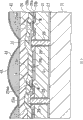
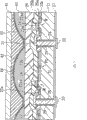
Fig. 2 is the part sectioned view of wanting portion to constitute that the present invention's the 1st embodiment solid state image sensor 1 is shown, and Fig. 1 is the local amplification profile of this imageing sensor 1.
As shown in Figures 1 and 2, this solid state image sensor 1 is a 3-tier architecture, possesses output layer 10, photo detector layer 20 and light introduced layer 40.This solid state image sensor 1 has a plurality of pixel region PX that are configured to the matrix array shape, with all pickup images of these pixel regions PX, is transformed into the signal of telecommunication and output.The flat shape of each pixel region PX is rectangle in the present embodiment, but also can be other shapes such as circle, hexagon certainly.
Light introduced layer 40 is taken into the light from the image that is positioned at imageing sensor 1 outside (external image), transmits to each pixel region PX of photo detector layer 20.Photo detector layer 20 imports light into layer 40 light that is taken into to each pixel region PX and is transformed into the signal of telecommunication corresponding with this light.Output layer 10 will be outputed to the outside of imageing sensor 1 by the signal of telecommunication that photo detector layer 20 obtains to each pixel region PX.Shu Chu the signal of telecommunication so for example is transferred into display unit and is used on its screen and shows external image, or is sent to signal processing apparatus arbitrarily, is used in the signal processing of regulation.
Light introduced layer 40, photo detector layer 20 and output layer 10 detailed formation separately below are described.
Photo detector layer 20 as Fig. 1 clearly shown in, have the p type single crystalline Si substrate 21 that lower surface is covered by dielectric film 27.On the upper surface of Si substrate 21, optionally be formed with insulated separation film 22, utilize this insulated separation film 22 to form and a plurality of one to one element-forming region of pixel region PX (active region).That is to say that these element-forming region are configured to the matrix shape identical with pixel region PX.
In the following description, the zone that will be formed with insulated separation film 22 claims " insulated separation zone ".Thereby, on the upper surface of Si substrate 21, exist the insulated separation zone and form zone (active region) with a plurality of pixels.
Inside in each element-forming region of Si substrate 21 forms MOS field-effect transistor (to call MOS transistor an in the following text) M and a photodiode PD.MOS transistor M and photodiode PD are electrically connected mutually.Photodiode PD is the semiconductor light-receiving device that the light that will be imported is transformed into the signal of telecommunication.MOS transistor M takes out the switching semiconductor element that the photodiode signal of telecommunication that PD generates is used from photo detector 20.
MOS transistor M is by leaving a pair of n that the compartment of terrain forms in Si substrate 21 inside
+Type source drain zone (S/D zone) 23a, 23b, the dielectric film 25aa of covering Si substrate 21 upper surfaces between S/ D zone 23a and 23b, and the gate electrode 24 that is formed on the dielectric film 25aa constitutes.Dielectric film 25aa is that dielectric film 25a is positioned at the part under the gate electrode 24, plays the effect of gate insulating film.Gate electrode 24 is disposed near element-forming region a certain (left side among Fig. 1) end.In these gate electrode 24 1 sides, wiring membrane 31 be formed at insulated separation film 22 above.This wiring membrane 31 contacts with a side source drain zone 23a (left side among Fig. 1) by the window that is formed at dielectric film 25a.Element forms the part of region surface except that this window and is covered by dielectric film 25a.
Photodiode PD is by another n
+The source drain zone 23b (right side among Fig. 1) and the p type single crystalline Si substrate 21 of type constitute.That is to say that the source drain zone 23b of the shared MOS transistor M of photodiode PD makes photodiode PD be electrically connected with MOS transistor M thus.Source drain zone 23b becomes the light area of photodiode PD.
The MOS transistor M and the photodiode PD that are formed at each element-forming region use interlayer dielectric 25b to cover.This interlayer dielectric 25b covers whole of Si substrate 21.Be formed with whole above the interlayer dielectric 25b than its thicker interlayer dielectric 26 covering Si substrates 21.The surface of interlayer dielectric 26 is for the formation that is easy to light introduced layer 40 and fixing, and smooth is parallel with Si substrate 21.
Interlayer dielectric 25b, 26 and dielectric film 25a with allowing the material of this imageing sensor 1 detectable light transmission (as SiO
2) form.Utilize light introduced layer 40 to import the exterior light of imageing sensor 1 inside, penetrate interlayer dielectric 25b, 26, dielectric film 25a, shine on the photodiode PD that is formed at photo detector layer 20 each element-forming region.Therefore, become transmission region with the position that each photodiode of interlayer dielectric 25b, 26, dielectric film 25a forms zone institute's corresponding (roughly repetition).As described later, light introduced layer 40 forms, is fixed on these transmission regions.
Among the 1st embodiment, the whole surface of photo detector layer 20 is a light-permeable, but this and inessential.Also a part of light-permeable on photo detector layer 20 surface.As long as the corresponding transmission region that exists with photodiode PD is just much of that on photo detector layer 20 surface.
On the position of insulated separation film 22 in Si substrate 21 (insulated separation zone), be formed with connect substrate 21 upper surfaces and lower surface a plurality of and bury wiring underground.These bury wiring underground, and each dielectric film 28 that is covered by the through hole madial wall to up/down perforation substrate 21 respectively, the filling dimpling electroplax 30 that forms that contacts in the conductivity plug 29 of these dielectric film 28 inboards, with the lower end of this conductivity plug 29 is constituted.The upper end of conductivity plug 29 contacts with wiring membrane 31 on being formed at insulated separation film 22, and this wiring membrane 31 and n
+The source drain zone 23a of type contacts, so this source drain zone 23a is electrically connected with dimpling electrode 30 by wiring membrane 31 and conductivity plug 29.
Among the 1st embodiment, use n-channel MOS transistor (nMOS) as switch with transistor, but also can use p-channel MOS transistor (pMOS), n-channel MOS transistor also capable of being combined and p-channel MOS transistor form complementary type MOS (CMOS) transistor and constitute.Transistor or other electronic components beyond the also available MOS transistor.
Light introduced layer 40 below is described.
Light introduced layer 40 form and be fixed in photo detector layer 20 interlayer dielectric 26 (in other words being the transmission region of photo detector layer 20) above.Light introduced layer 40 has and utilizes supporting walls to be bearing in interlayer dielectric 26 through the tabular quartz cover 51 on the smooth upper surface.The lower end of abutment wall 50 and upper end are individually fixed in the upper surface of interlayer dielectric 26 and the inner surface of lid 51.
Utilize abutment wall 50, be formed with cavity 42 between interlayer dielectric 26 and lid 51, the inside of this cavity 42 disposes a plurality of lenticules 43 by matrix shape.These lenticules 43 and the corresponding one by one configuration of pixel region PX, in other words, in photo detector layer 20, have photodiode PD element-forming region directly over overlap configuration respectively with them.
The flat shape of lid 51, consistent with the flat shape of this imageing sensor 1 here, be rectangle, but also can be other shape.The flat shape of cavity 42, for lid 51 flat shapes identical rectangle, but also can be other shapes.The flat shape of lenticule 43 is circular here, but also can be other shapes.The height of lenticule 43 for example is 1 μ m~3 μ m.
Abutment wall 50 is extended along the whole edges of rectangular cap 51 and is distributed to delimit the outward flange of cavity 42, also partly extends simultaneously to be distributed in cover position (i.e. inboard) beyond 51 the edge.Abutment wall 50 is owing to establishing for forming cavity 42, so also can an edge configuration along rectangular cap 51 form.But the mechanical strength of light introduced layer 40 probably has deficiency like this.Therefore consider this point, the position beyond the edge of lid 51 (promptly inboard) is in suitable position clathrate ground configuration abutment wall 50, to solve the problem of its undercapacity.
Abutment wall 50 is expressed as Fig. 1, is formed by aluminium (Al) film 44, bonding agent 45, single crystalline Si sheet 41, bonding agent 46, has 4 layers of structure.This results from the manufacturing process of light introduced layer 40.The detailed content of its manufacturing process will be narrated in the back.
Al film 44 utilizes evaporation or sputtering method to form with the thickness of stipulating with the state that covers lenticule 43 on the entire upper surface of interlayer dielectric 26 usually.Therefore, even without bonding agent, Al film 44 also is fixed in the surface of the upper surface and the lenticule 43 of interlayer dielectric 26.Al film 44 on the lenticule 43 utilizes etching to remove, and the Al film 44 between the lenticule 43 is etched and left behind.The part of the Al film of being removed by this etching 44 not constitutes the part of abutment wall 50.
Above the Al film 44, fixing the single crystalline Si sheet 41 of specific thickness with bonding agent 45.Si sheet 41 is removed by etching selectivity ground in order to form cavity 42, the part of the Si sheet 41 of etched removal not, another part of formation abutment wall 50.
Quartz cover 51 usefulness bonding agents 46 be fixed in Si sheet 41 above, utilize this to cover the whole upper opening of 51 closed cavities 42.Its result, cavity 42 delimited by interlayer dielectric 26, abutment wall 50 and quartz cover 51.And abutment wall 50 becomes 4 layers of structure of Al film 44, bonding agent 45, single crystalline Si sheet 41, bonding agent 46.
Form the quartz glass of quartz cover 51, to having light transmission, so outside luminous energy enters in the cavity 42 by covering 51 by the light that this imageing sensor 1 detects.Then, enter exterior light in the cavity 42 behind lenticule 43 optically focused, connect and pass interlayer dielectric 26,25b and dielectric film 25a, shine to the photodiode PD of each element-forming region by each pixel region PX.
Output layer 10 below is described.
Output layer 10 is to be used for the signal of telecommunication that photo detector layer 20 corresponding irradiated exterior light the are generated layer to this imageing sensor 1 outside output.This output layer 10 has two single crystalline Si substrates 11 that the surface is covered respectively by dielectric film 13 and 12 up and down.Be formed with on this Si substrate 11 that (being up/down perforation Si substrate 11) that connect its upper surface and lower surface is a plurality of buries wiring underground.These bury wiring underground, and each has the dielectric film 14 of the madial wall of the through hole that covers up/down perforation Si substrate 11, the conductivity plug 15 of filling dielectric film 14 inboards and the dimpling electrode 17 and 16 that contacts and form with the upper and lower side of this conductivity plug 15.
Between the Si substrate 11 of output layer 10 and the Si substrate 21 of photo detector layer 20, overlap welding by dimpling electroplax 17 with 30, and filling bonding agent 61 is fastened to each other in the gap between two substrates 11 and 21 with correspondence.Si substrate 11 and 21 is parallel to each other.As bonding agent 61, can suit to use polyimide resin, epoxy resin etc.
In the solid state image sensor of the 1st embodiment, there is not semiconductor element in Si substrate 11 inside of output layer 10, and Si substrate 11 only uses as the base material of burying wiring underground.Therefore the conductivity type of Si substrate 11 is arbitrarily, can think the n type, also can be the p type, also can be for not containing the i type of dopant.But as the 2nd and the 3rd embodiment that narrates later, when forming semiconductor element, then need to select the conductivity type of Si substrate 11 so that meet the formation of this semiconductor element in Si substrate 11 inside.The action of solid state image sensor
Below explanation has the action of the 1st embodiment solid state image sensor 1 of above formation.
At first, make imageing sensor 1 shooting face, be the surface of the quartz cover 51 of light introduced layer 40, towards the object of required shooting, place near this shooting object.So the light (exterior light) that this shooting object is sent is taken into the inside (being cavity 42) of imageing sensor 1 by quartz cover 51.On the photodiode PD that utilize light optically focused that the lenticules 43 in the cavity 42 will be taken into, shines photoreceptor layer 20.Each pixel region PX is carried out this optically focused, irradiation.
The light that photodiode PD in each pixel region PX will receive like this carries out light-to-current inversion, generates the signal of telecommunication of corresponding its luminous intensity.This signal of telecommunication is sent to output layer 10 by the switch that is connected to photodiode PD with MOS transistor M.That is, when taking out the signal of telecommunication, switch becomes ON (conducting) state with MOS transistor M, and its signal of telecommunication is sent to the lower surface (outside of photo detector layer 20) of Si substrate 21 by wiring membrane 31, conductivity plug 29 and the dimpling electrode 30 of photo detector layer 20.This signal of telecommunication and then dimpling electrode 17 and conductivity plug 15 by output layer 10 are sent to the dimpling electrode 16 that is positioned at solid state image sensor 1 lowest surface, like this, and just can be from the dimpling electrode 16 taking-up signals of telecommunication of output layer 10.
Among this 1st embodiment, the dimpling electrode 16 of output layer 10 plays the effect of the output of this solid state image sensor 1.
Like this, the output signal of telecommunication of the 1st embodiment solid state image sensor 1 is by at its lowest surface being dimpling electrode (output) 16 outputs that array-like is arranged in the bottom surface.Therefore, we can say that this imageing sensor 1 possesses and so-called " area array encapsulation " equal structure.
Figure 13 illustrates the circuit diagram that circuit constitutes in each pixel region PX.As shown in Figure 13, the negative electrode of photodiode PD is connected to one of source drain zone of MOS transistor M.And the gate electrode of MOS transistor M is connected with holding wire W with holding wire B respectively with another source drain zone.Sort circuit constitutes well-known, therefore no longer adds explanation here.The method for making of solid state image sensor
Then, with reference to Fig. 3~Figure 12, the manufacture method of the present invention's the 1st embodiment solid state image sensor 1 with above-mentioned formation is described.
At first, as shown in Figure 3, preparing Jie (is SiO at dielectric film here
2Film) pastes 2 single crystalline Si substrates 71 and 21 SOI that form (Silicon On Insulator: substrate insulator silicon).Then, with the known method inside and the required a plurality of element-forming region of the corresponding formation of pixel region PX of Si substrate 21 up.And then at the inside of each element-forming region formation MOS transistor M and photodiode PD, and form the wiring of burying underground that is connected with these MOS transistor M.So just, obtain formation shown in Figure 3.
The method that obtains formation shown in Figure 3 is arbitrarily, formation for example as described below.
Earlier on the surface of the p type Si substrate 21 of formation SOI substrate, optionally form insulated separation film (SiO for example with known method
2Film) 22, thus the delimitation of array-like ground forms the zone with a plurality of pixel region PX corresponding elements on the surface of this Si base version 21.Next on insulated separation film 22, form a plurality of through holes of up/down perforation Si substrate 21 with known method.At this moment, the dielectric film under these through holes 27 is also partly removed, made the bottom of through hole be exposed to Si substrate 71 1 sides with known method.After covering these through hole madial walls with dielectric film 28 then, filling conductivity plug 29 in these through holes.At this moment, expose from the upper end of through hole the upper end of conductivity plug 29, and the lower end of conductivity plug 29 then contacts with Si substrate 71.Like this, insulated separation film 22 existing zones (being the insulated separation zone) formed the wiring of burying underground of formation shown in Figure 3.
Then, in each element-forming region, form dielectric film 25a on the surface of Si substrate 21 with known method.Then on dielectric film 25a, form gate electrode (for example polysilicon system) 24 selectively.The position that dielectric film 25a is positioned under the gate electrode 24 becomes gate insulating film 25aa.At this moment, in each element-forming region, all surfaces of Si substrate 21 is covered by dielectric film 25a.Then, form a pair of n with known method in Si substrate 21 inside
+The source drain zone 23a and the 23b of type finish MOS transistor M.
Herein, then with known etching method leave on the dielectric film 25a with bury wiring underground near behind the window that communicates of the regional 23a of a side source drain, at dielectric film 25a and the wiring membrane 31 of formation optionally above the insulated separation film 22 with conductivity.At this moment, wiring membrane 31 contacts with the regional 23a of source drain by the window of dielectric film 25a on the one hand, on the other hand with the last end in contact of conductivity plug 29.Therefore, source drain zone 23a is electrically connected by wiring membrane 31 with conductivity plug 29.
Then, with interlayer dielectric 25b cover gate electrode 24 and wiring membrane 31, and then form interlayer dielectric 26 thereon.(Chemical Mechanical Polishing: chemico-mechanical polishing) surface of method or etching method grinding interlayer dielectric 26 makes it smooth to use CMP then.Obtain structure shown in Figure 3 like this.
Then, in the structure of Fig. 3, form the used film of lenticule 43 through smooth whole surface at interlayer dielectric 26.As the material of this film, can make suitably with photoresist, organic material such as organic polymer, perhaps polysilicon, silica (SiO
2), silicon nitride inorganic material such as (SiNx), form the film of specific thickness with methods such as coatings, sputter, CVD.
With photoresist or organic high molecular layer when forming lenticule 43, utilize photoetching process or etching method that this film is patterned into the island type part of circular, then in addition heat treatment.So the surface curvature of these island type parts becomes protruding spherical shape, becomes the lenticule 43 that covers each element-forming region as shown in Figure 4.
When forming lenticule 43 with inorganic material films such as polysilicon, silica, silicon nitrides, on this inorganic material film, form the photoresist film (photoresist pattern) that is patterned into required microlens shape, with this photoresist film as mask, the described inorganic material film of etching optionally.Like this, by with described photoresist pattern transfer to described inorganic material film, form the island type part of circular.These island type parts just become lenticule 43.
Form the lenticule 43 that obtains with above-mentioned 2 kinds of methods, on the flat surfaces of interlayer dielectric 26 with the corresponding one by one array-like that is configured to of pixel region PX.
Then, form Al film 44 at interlayer dielectric 26 through the whole state with the lenticule 43 that covers previous formation on the smooth whole surface with methods such as evaporation, sputters.The thickness of Al film 44 for example is 100nm~400nm.At this moment state as shown in Figure 4.As shown in Figure 4, Al film 44 major parts are positioned on the lenticule 43, but the gap of 43 of the lenticule of a part by adjacency contacts with the surface of interlayer dielectric 26 and fixes.
Then, as shown in Figure 5 on Al film 44 with specific thickness adhesive-applying 45.At this moment, for easy bonding single crystal Si sheet 41, carry out smooth to the bonding agent 45 that applies with known method.So just, obtain structure shown in Figure 5.On the surface of this bonding agent 45, paste the single crystalline Si sheet 41 of specific thickness (for example about 100 μ m~1000 μ m) then.This Si sheet 41 is used to form the part of the abutment wall 50 of cavity 42.The state of this moment as shown in Figure 6.
Be affixed on the single crystalline Si sheet 41 on bonding agent 45 surfaces, its surface is reached desired thickness by grinding.The thickness of the substrate 41 after the grinding is for example 50 μ m~200 μ m.At this moment state as shown in Figure 7.
In addition, in the present embodiment, use single crystalline Si sheet 41 in order to form cavity 42, but be not limited to this.Much less, so long as have good processabilities such as desired stiffness and etching, the sheet that also available other any materials are made.
, utilize to grind or etching remove be arranged in Fig. 6 structure undermost Si substrate 71 integral body, the dielectric film 27 that is positioned at 21 of Si substrate 71 and Si substrates is exposed thereafter.Then, form in the lower end of the conductivity plug 29 of respectively burying wiring underground with known method and fixing dimpling electrode 30.At this moment state as shown in Figure 7.
As mentioned below, Al film 44 is used for when etching monocrystalline silicon piece 41 and bonding agent 45, protection lenticule 43 in the bottom, and in other words, Al film 44 is to use as etch stop layer at this moment.Therefore, as long as can obtain such function, can use Al any film in addition.
On the other hand, in order to make output layer 10, prepare Jie as shown in Figure 8 and (be SiO here at dielectric film
2Film) 12 paste 2 single crystalline Si substrates 81 and the 11 SOI substrates that form.Then, form a plurality of through holes of up/down perforation substrate 11.At this moment, also partly remove the dielectric film 12 under these through holes, make the bottom of through hole be exposed to Si substrate 81 1 sides.After covering the madial wall of through hole with dielectric film 14 then, filling conductivity plug 15 in these through holes.At this moment, expose from the upper end of through hole the upper end of conductivity plug 15, and the surface of the following end in contact Si substrate 81 of conductivity plug 15.And, form in the upper end of the conductivity plug 15 of respectively burying wiring underground and fixing dimpling electrode 17.So just, obtain the wiring of burying underground of formation shown in Figure 8.
Then, as shown in Figure 9, be aligned with each other dimpling electrode 30 and dimpling electrode 17, and meanwhile on dimpling electrode 17 1 sides of Si substrate 11 shown in Figure 8 the structure of mounting Fig. 7.At two interstructural clearance filled bonding agents 61, make two structures fastened to each other then.Make dimpling electrode 30 and dimpling electrode 17 welding each other again.Under this state, remove the whole of Si substrate 81, dielectric film 12 and conductivity plug 15 are exposed by grinding or etching.
And then, form in the lower end of each conductivity plug 15 and fixing dimpling electrode 16, obtain structure shown in Figure 11.At this moment, just become bonding photo detector layer 20 on the output layer 10, and plant the state that is equipped with the lenticule 43 that forms light introduced layer 40 etc. on the photo detector layer 20.
Here, with the suitable mask uppermost Si sheet 41 of etching optionally, in Si sheet 41, form through hole.Then, remove the bonding agent 45 that is positioned at below the Si sheet 41 by etching selectivity with same mask.In these two etching work procedures, Al film 44 plays the effect of etching obstacle, thereby is positioned at the influence that lenticule 43 below it is not subjected to etching action.Therefore, lenticule 43 positively obtains protection.
Next, use same mask, by etching selectivity remove the Al film 44 that exposes in these through holes.So just, obtain state shown in Figure 12.Under this state, cavity 42 forms basically, and lenticule 43 is exposed in the cavity 42 simultaneously.
At last, on be used to form the Si sheet 41 of cavity 42, with the bonding agent 46 bonding rectangular cap of making by quartz glass 51, thus the closed interior space.So just, form the abutment wall 50 and the cavity 42 of light introduced layer 40.
Through above operation, just can obtain the solid state image sensor 1 of 3-tier architecture as depicted in figs. 1 and 2.
Cover 51 light transmission rate in order to avoid as far as possible reducing, as shown in the figure, bonding agent 46 can only be configured in the upper end of abutment wall 50.But, also can be coated in and cover on 51 the total inner surface in order to simplify the working procedure of coating of bonding agent.At this moment, because the existence of bonding agent 46, light transmission rate has a little to reduce, but is adjustable to the degree of the problem that do not take place in the practicality.
In addition, the manufacture method of output layer 10 is not limited to method described here, much less also available other any means.
As previously discussed, the solid state image sensor 1 of the present invention the 1st embodiment possesses the element layer of being subjected to 20, light introduced layer 40 and output layer 10 and constitutes.And, light introduced layer 40 comprises a plurality of lenticules 43, abutment wall 50 and light transmission quartz cover 51, and the exterior light that import cavitys 42 inside by light transmission lid 51 shine via lenticule 43 that semiconductor light-receiving devices are on the photodiode PD in the photo detector layer 40.
Like this, the solid state image sensor 1 of the 1st embodiment becomes with respect to the photo detector layer 20 that contains photodiode PD, is combined with the structure of the output layer 10 that imports light introduced layer 40 that exterior light uses and the output and the corresponding signal of telecommunication of this exterior light.And the light introduced layer 40 that is used to import exterior light comprises by abutment wall 50 and light transmission lid 51 cavitys that form 42 and is disposed at a plurality of lenticules 43 in this cavity 42, so light introduced layer 40 plays the effect that lenticule 43 is encapsulated.Therefore we can say that the solid state image sensor 1 of the 1st embodiment has the formation that this light importing is formed one with encapsulation and optical element layer 20 and output layer 10.
In addition, because lenticule 43, abutment wall 50 and the cavity 42 of light introduced layer 40 can utilize the known Micrometer-Nanometer Processing Technology of using in the semiconductor device manufacturing to form,, become die size so the light that comprises lenticule 43 is imported with encapsulating miniaturization.That is to say, the light of solid state image sensor 1 ancillary chip size is imported with encapsulation.
Aspect manufacture method, because having, solid state image sensor 1 will form constituting of one by the 40 formed encapsulation of light introduced layer and photo detector layer 20 and output layer 10, so do not need to become encapsulation semiconductor chip to be installed on such operation in this encapsulation afterwards with the sub semiconductor chip open form, manufacturing process simplifies again.And lenticule 43 is not the surface that is formed at quartz glass layer, but is formed at above the interlayer dielectric 26 of photo detector layer 20, so the height technology not requiring as on being formed at the quartz glass surface time.
And the making of photo detector layer 20 and output layer 10 can be used known laminated technology that the laminated formation three-dimensional structure of a plurality of semiconductor chips is used (aligned position comes laminated technology with bonding agent with substrate is bonding mutually on one side) on one side.Thereby, forming as one both are laminated then as long as form photo detector layer 20 and output layer 10 with semiconductor chip respectively, photo detector layer 20 also is easy to the making of output layer 10.
Thereby, solid state image sensor 1, it makes the technology that does not need special height, can easily make.
From the operating rate aspect, the lenticule 43 of light introduced layer 40 is because near being disposed on the transmission region of photo detector layer 20, so can will be transformed into the signal of telecommunication immediately by the exterior light of lenticule 43 by photodiode PD.This signal of telecommunication can be exported to the outside by output layer 10 immediately from photo detector layer 20.Therefore, can fully shorten the length of arrangement wire that the conversion exterior light is obtained the signal of telecommunication.And this signal of telecommunication does not need to use CCD to pass on one by one yet.Thereby, the sufficiently high operating rate (for example operating frequency of the GHz order of magnitude) that the requirement that can obtain improving with conversion speed in recent years adapts.
From function aspects, in the solid state image sensor 1, can easily realize as required with various circuit such as the amplifying circuit of input electrical signal and signal processing circuit join photo detector layer 20 or output layer 10 or this two-layer among, the signal processing circuit layer that maybe will comprise the desired signal treatment circuit separately forms and joins between photo detector layer 20 and the output layer 10.Thereby, can be as required various required circuit such as the amplifying circuit of input electrical signal and signal processing circuit be joined in the solid state image sensor 1.
Like this, utilize the present invention the 1st embodiment, can access high speed, high sensitivity and high performance microminiature solid state image sensor 1.
In addition, be formed at the dielectric film 27 of photo detector layer 20Si substrate 21 lower surfaces, might not need.This is because as long as use the bonding agent 61 of insulating properties, just can guarantee the electric insulation between photo detector layer 20 and the output layer 10.This for the dielectric film 13 of output layer 10 too.
Handle the occasion of output again and carry out desired signal earlier, also can the signal processing circuit layer that comprise the desired signal treatment circuit be set at photo detector layer 20 and output layer 10 at the signal of telecommunication that exterior light is obtained through light-to-current inversion.The available formation that communicates with photo detector layer 20 of this signal processing circuit layer easily realizes, so omit its detailed explanation at this.
In addition, be provided with output layer 10 among above-mentioned the 1st embodiment, select to refer to that layer replaces output layer 10 but much less plug-in type also can be set.
The 2nd embodiment
Figure 14 illustrates the formation of the present invention the 2nd embodiment solid state image sensor 1A.
This imageing sensor 1A is equivalent in the 1st embodiment solid state image sensor 1 switch be moved to output layer 10 with MOS transistor M from photo detector layer 20, and formation in addition is identical.Therefore, give the symbol identical, omit its relevant explanation with the 1st embodiment solid state image sensor 1 to inscape corresponding among Figure 14.
As shown in figure 14, solid state image sensor 1A also is the 3-tier architecture identical with the 1st embodiment solid state image sensor 1.
In the photo detector layer 20 ', be formed with n respectively in a plurality of element-forming region that on p type single crystalline Si sheet 21, form
+Type diffusion zone 23.That is, only form photodiode PD.This point is different from the solid state image sensor 1 of the 1st embodiment.Therefore, the almost whole face of each element-forming region becomes the face that can be subjected to light, and promptly almost whole of each element-forming region is " but light area ".Therefore have advantage, can " take factor (Fill Factor), i.e. the light-receiving area ratio shared " and be set near 100% with respect to elemental area.Other formation is identical with the solid state image sensor 1 of the 1st embodiment.
In addition, in the 1st embodiment solid state image sensor 1,, make that " but light area " is corresponding to be reduced owing to have MOS transistor M in each element-forming region.That is to say that compare with the 2nd embodiment solid state image sensor 1A, " taking factor " can reduce.
In the output layer 10 ', on single crystalline Si sheet 11, be formed on the MOS transistor M that is formed in the 1st embodiment solid state image sensor 1 in the photo detector layer 20.That is to say that output layer 10 ' has the p type single crystalline Si substrate 11 that lower surface covers with dielectric film 12 as shown in figure 14.On the upper surface of Si substrate 11, optionally be formed with insulated separation film 22 ', utilize this insulated separation film 22 ', with the pixel region PX a plurality of element-forming region of corresponding one by one formation (active region).That is to say that these element-forming region are configured to the matrix shape identical with pixel region PX.
Inside in each element-forming region of Si substrate 11 is formed with at least one MOS transistor M.This MOS transistor M is by leave a pair of n that the compartment of terrain forms in the inside of Si substrate 11
+The dielectric film 25a ' of type source drain zone (S/D zone) 23a ', 23b ', covering Si substrate 11 upper surfaces and the gate electrode 24 ' that is formed at above the dielectric film 25a ' constitute.Dielectric film 25a ' is positioned at the effect that part 25aa ' under the gate electrode 24 plays gate insulating film.Be formed with wiring membrane 31 ' on insulated separation film 22 ', this wiring membrane 31 ' is gone up the window that forms and is contacted with a side source drain zone 23a ' (left side among Figure 14) by dielectric film 25 '.The part of the surface of element-forming region except this window uses dielectric film 25a ' to cover.
The MOS transistor M that is formed at each element-forming region of Si substrate 11 is insulated film 13 and is covered with.This dielectric film 13 covers whole of Si substrate.The surface of dielectric film 13 is easy in order to make with the set of photo detector layer 20 ', can smoothly be parallel with Si substrate 11.
The inside of dielectric film 13 is embedded with conductivity plug 18 directly over the insulated separation film 22 ' of each element-forming region.The top and bottom of this conductivity plug 18 contact with corresponding dimpling electrode 17 and wiring membrane 31 ' respectively.
Insulated separation film 22 ' is gone up the wiring membrane 31 ' that forms, and contacts the upper end of conductivity plug 15 on the one hand, contacts n on the other hand
+Type source drain zone 23a ', therefore, source drain zone 23a ' is electrically connected with dimpling electrode 16 with conductivity plug 15 by wiring membrane 31 '.In addition, wiring membrane 31 ' is owing to the lower end that touches the conductivity plug 18 that forms in the dielectric film 13, so also be electrically connected with diffusion zone 23.Like this, each photodiode PD of photo detector layer 20 ' is electrically connected with the corresponding MOS transistor M of output layer 10 '.
In addition, the MOS transistor of only drawing in the output layer 10 ' among Figure 14, but also can carry a plurality of transistors to constitute amplifying circuit, signal processing circuit or memory circuit.Also can make the multilayer output layer, in each layer, add required circuit respectively.
The solid state image sensor 1A of the present invention the 2nd embodiment, the available and roughly the same method manufacturing of the 1st embodiment manufacture method.That is, photo detector layer 20 ' obviously can be made with the photo detector layer 20 of the 1st embodiment roughly the samely.And output layer 10 ', as long as form MOS transistor M equally with the situation of the photo detector layer 20 of the 1st embodiment on Si substrate 11, other operations can be made in the same manner with the situation of the output layer 10 of the 1st embodiment.Therefore, its detailed description is omitted.
The solid state image sensor 1A of the present invention the 2nd embodiment owing to be as above to constitute, so much less, can obtain the effect identical with the 1st embodiment solid state image sensor 1.But can also obtain following effect among the solid state image sensor 1A.
Usually utilize the solid state image sensor of CCD, its where the shoe pinches is, can improve " taking factor ", but can't accelerate operating rate, also can't handle (needing its special circuit in addition) to amplification of input signal etc.On the other hand, resemble the present invention photodiode and the MOS transistor solid state image sensor as photo detector, its difficulty is, can obtain at a high speed, the sort of performance of high sensitivity, and can carry out processing such as amplification to input signal, but be difficult to improve and take factor.
Utilize the solid state image sensor of the present invention the 2nd embodiment, then can have the feature (advantage) of these two kinds of situations concurrently.That is to say, at a high speed, the highly sensitive while can improve and take factor, and realize high image resolution.And, owing to can carry out to processing such as the amplification of input electrical signal and computings, so also realize high-performance easily.
Plug-in type also can be set among above-mentioned the 2nd embodiment select to refer to that layer replaces output layer 10 '.
The 3rd embodiment
Figure 15 illustrates the formation of the present invention the 3rd embodiment solid state image sensor 1B.
This imageing sensor 1B is equivalent among the solid state image sensor 1A of the 2nd embodiment in Figure 14 at photo detector layer 20 " inside be provided with and be subjected to light to replace the situation of photodiode PD with MOS transistor (photistor) M ', formation in addition is identical.And photo detector layer 20 " formation MOS transistor M with output layer 10 ' except that turned upside down of MOS transistor M ' identical in fact.
As shown in figure 15, this solid state image sensor 1B also is a 3-tier architecture, photo detector layer 20 " in, a plurality of element-forming region that form in single crystalline Si substrate 21 lower surfaces one side are formed with a pair of source electrode drain region 23a, 23b respectively.This point is different from solid state image sensor 1 and the 1A of the 1st embodiment and the 2nd embodiment.
Among the solid state image sensor 1B, MOS transistor M ' turned upside down as photo detector is disposed in each element-forming region, so almost whole of available each element-forming region is subjected to light, that is to say that the almost whole face of each element-forming region becomes " but light area ".Thereby identical with the 2nd embodiment, its advantage is, can set " taking factor " near 100%.In addition, the exterior light that is taken into of light introduced layer is by photo detector layer 20 " Si substrate 21 shine MOS transistor M '.
Photo detector layer 20 " MOS transistor M ', leave a pair of n that the compartment of terrain forms in inside by side below Si substrate 21
+Type source drain zone 23a, 23b cover the dielectric film 25a of Si substrate 11 lower surfaces and the gate electrode 24 that is formed under the dielectric film 25a constitutes.Dielectric film 25a is positioned at the effect that position 25aa under the gate electrode 24 plays gate insulating film.Wiring membrane 31 is formed at below the insulated separation film 22.This wiring membrane 31 contacts with a certain source drain zone 23a (being the left side among Figure 15) by the window that is formed at dielectric film 25a.The position of the surface of element-forming region except window covers with dielectric film 25a.
The lower surface of MOS transistor M ' that is formed at each element-forming region of Si substrate 21 is all covered by dielectric film 25c.This dielectric film 25c covers whole of Si substrate 21.The surface of dielectric film 25c is in order to be easily fixed in output layer, and smooth is parallel with Si substrate 21.
The inside of dielectric film 25c is embedded with conduction condition rod 19 under the dielectric film 22 of each element-forming region.The top and bottom of this conductivity plug 19 contact with dimpling electrode 30 with corresponding wiring membrane 31 respectively.
In the output layer 10 ', be formed at the wiring membrane 31 ' on the insulated separation film 22 ', on the one hand with the following end in contact of conductivity plug 18, on the other hand with n
+23a ' the contact of type source drain zone is so source drain zone 23a ' is electrically connected with dimpling electrode 17 with conductivity plug 18 by wiring membrane 31 '.Dimpling electrode 17 is electrically connected owing to contacting with dimpling electrode 30, thereby photo detector layer 20 " source drain zone 23a by conductivity plug 19, dimpling electrode 30,17, conductivity plug 18 and wiring layer 31 ', be electrically connected with the source drain zone 23a ' of output layer 10 '.
Like this, photo detector layer 20 " each MOS transistor M ' of used by light, can with output layer 10 ' inductive switch is electrically connected with MOS transistor M.
In addition much less, also available photodiode replacement is subjected to light MOS transistor M '.
The manufacture method of the solid state image sensor 1B of the 3rd embodiment use the 1st capable of being combined and the 2nd embodiment is easily made.Simple declaration one this manufacture method of example is as follows.
Earlier make photo detector layer 20 respectively with different single crystalline Si substrates " and output layer 10 '.That is to say photo detector layer 20 " with SOI substrate shown in Figure 3 as Si substrate 21 (the also Si substrate of available routine).On the surface of Si substrate 21, with known method form shown in Figure 15 be subjected to light to use MOS transistor M ' and wiring membrane 31 after, on the surface of Si substrate 21, form dielectric film 25c, cover and be subjected to light MOS transistor M '.In dielectric film 25c, bury conductivity plug 19 then underground, smooth back is carried out on the surface of dielectric film 25c form dimpling electrode 30.
On the other hand, output layer 10 ' is same as shown in Figure 8, uses the SOI substrate that is made of Si substrate 11 and 81 to make.That is to say, be formed with switch MOS transistor M with the element-forming region of known method on Si substrate 11 surfaces.Then, after forming wiring membrane 31 ', cover MOS transistor M and wiring membrane 31 ' with dielectric film 13.After in dielectric film 13, burying conductivity plug 18 underground, make the dielectric film surfacing.Then form dimpling electrode 17.
But Fig. 8 situation (the 1st embodiment) does not form switch MOS transistor M in element-forming region, but is formed with switch MOS transistor M at the output layer 10 ' of the 3rd embodiment.In addition, when carrying amplifying circuit or signal processing circuit, much less, as required except switch with also making a plurality of MOS transistor etc. the MOS transistor M.
Next, will have the photo detector layer of as above making 20 " with the Si substrate 21 and 71 of structure,, the face that forms a MOS transistor M and a M ' side is fitted in opposite directions with Si substrate 11 and 81 with output layer 10 ' usefulness structure.During applying, as shown in figure 15, make to be positioned at and have photo detector layer 20 " with the dimpling electrode 30 on the surface of the Si substrate 21 of structure; be positioned at have output layer 10 ' with the dimpling electrode 17 on the surface of the Si substrate 11 of structure mutually in opposite directions aligning contact; make a part of welding of these dimpling electrodes 30 and 17, and in addition combination.Then, the dielectric film 25c on Si substrate 21 and above the Si substrate 11 in the gap between the dielectric film 13 filling bonding agent 61 fix.
Then,, remove photo detector layer 20 fully by grinding or etching " the Si substrate 71 and the dielectric film 27 of a side, remove Si substrate 21 from back portion simultaneously, fully reduce its thickness until the degree that can accept institute's light requirement.
Next,, on the back side of the Si substrate 21 that has reduced thickness, form interlayer dielectric 26, form lenticule 43 and Al film 44 it on, by bond layer 45 bonding single crystalline Si sheets 41 with Fig. 4~shown in Figure 7 identical.
Utilize grinding or etching to remove fully then and have the Si substrate 81 of output layer 10 ', the dielectric film 12 and the lower end of conductivity plug 15 are exposed with Si substrate 11 1 sides of structure from the back side.Then, the end portion at the conductivity plug 15 that exposes forms dimpling electrode 16.
At last, with method same as shown in Figure 12, after formation cavity 42 and the abutment wall 50, bonding quartz glass 51 as lid forms light introduced layer 40.So just, obtain structure shown in Figure 15.
The solid state image sensor 1B of the present invention the 3rd embodiment owing to be aforesaid formation, much less can obtain the same effect with the 2nd embodiment solid state image sensor 1A.
As mentioned above, among the 3rd embodiment solid state image sensor 1B, use MOS transistor (photistor) M ' from its gate electrode 24 opposite side irradiates lights to being subjected to light.Thereby this point is different with the solid state image sensor 1 of the 1st embodiment.
Among the solid state image sensor 1B of the 3rd embodiment, also can use photodiode to replace photistor M '.Like this, just, Si substrate that can be by being formed with this photodiode is to this photodiode irradiates light.Thereby this point is different with the 2nd embodiment solid state image sensor 1A.
To above-mentioned the 3rd embodiment, plug-in type also can be set select to refer to that layer replaces output layer 10 '.
The 4th embodiment
Figure 16 illustrates the formation of the present invention the 4th embodiment solid state image sensor 1C.
This imageing sensor 1C is different with above-mentioned the 1st~the 3rd embodiment, and light introduced layer 40A does not have cavity.In addition, select to refer to be provided with between layer 10A semiconductor element layer 90 of built-in regulation semiconductor element (not shown) in photo detector layer 20 and plug-in type.These semiconductor elements are electrically connected with the electrode 30 of being located at semiconductor element layer two surfaces about in the of 90 as required.Other constitute owing to identical with above-mentioned the 1st embodiment, so its explanation is omitted.
As shown in figure 16, the light introduced layer 40A among the 4th embodiment to comprise the light transmission body be tabular light transmission lid 51A, be integrally formed at the inside of this light transmission lid 51A and on the transmission region of photo detector layer 20 with a plurality of lenticules 43 of the corresponding configuration of a plurality of pixel region PX.As can be seen from Figure 16, there is not cavity in the inside of light transmission lid 51A.Light transmission lid 51A forms with any light transmission sheet materials such as quartz plates.
Following have the manufacture method of the 4th embodiment solid state image sensor 1C of above formation with reference to Figure 17 and Figure 18 explanation.
At first, identical with the 1st embodiment situation, obtain the photo detector layer 20 of formation shown in Figure 17.The detailed formation of photo detector layer 20 shown in Figure 17 is except being provided with at lower surface the electrode 30, all identical with Fig. 3.
In addition, utilize known method to form a plurality of lenticules 43 in the inside of the light transmission lid 51A that constitutes by quartz plate etc.For example, the one side of removing quartz plate by section circular arc by etching selectivity ground forms a plurality of recesses.The suitable lens material of filling in these recesses just can obtain burying underground the also light transmission lid 51A of built-in a plurality of lenticules 43 then.
Then, with the light transmission lid 51A that obtains like this, be fixed in the surface of photo detector layer 20 with bonding agent 52A.At this moment, carry out both location, make a plurality of lenticule 43 overlay configuration in the photo detector layer 20 pixel region PX corresponding with each transmission region.And, at the following table surface forming electrode 30 of photo detector layer 20.At this moment state as shown in figure 17.
Plug-in type selects to refer to that layer 10A uses the method identical with formation output layer 10 method therefors among the 1st embodiment to make.Semiconductor element layer 90 can use the method identical with formation photo detector layer 20 method therefor among the 1st embodiment to make.Place plug-in type to select to refer to be fixed on the layer 10 semiconductor element layer 90 with bonding agent 61 then.At this moment state as shown in figure 18.
At last, select to refer to above the semiconductor element layer 90 (with reference to Figure 18) layer above the 10A being fixed in plug-in type, fix with bonding agent 61 and light transmission is covered 51A be fixed on lip-deep photo detector layer 20 (with reference to Figure 17).Like this, can obtain the solid state image sensor 1C of the 4th embodiment shown in Figure 16.
The also available following method manufacturing of the solid state image sensor 1C of the 4th embodiment.With reference to Figure 19 and Figure 20 this method is described.
Plug-in type selects to refer to that layer 10A uses the method identical with formation output layer 10 method therefors among the 1st embodiment to make.The method that semiconductor element layer 90 usefulness are identical with formation photo detector layer 20 method therefor among the 1st embodiment is made.Place plug-in type to select to refer on the layer 10 fixing semiconductor element layer 90 with bonding agent 61 then.Operation so far is with identical with the above-mentioned manufacture method of Figure 17~Figure 18 explanation.Then, bearing substrate (for example quartz plate) 92 usefulness ultraviolet light degradation type bonding agents 93 are fixed in the upper surface of semiconductor element layer 90 after, select to refer in plug-in type to form electrode 16 on the lower surface of layer 10A.At this moment the formation operation of electrode 16 is limits selects to refer to that by plug-in type the laminated body limit that layer 10A and semiconductor element layer 90 constitute carries out with bearing substrate 92 supportings.At this moment state as shown in figure 19.
Then, to the ultraviolet ray of the 93 irradiation regulations of the ultraviolet light degradation type bonding agent after the sclerosis, bonding agent 93 just carries out chemical breakdown.Its result, can not to around cause under the dysgenic situation and easily bearing substrate 92 separated with semiconductor element layer 90.Here, on the surface of semiconductor element layer 90, form electrode 17.At this moment state as shown in figure 20.
On the other hand, by with the identical method of above-mentioned manufacture method with Figure 17~Figure 18 explanation, forms the laminated body that plug-in type selection shown in Figure 16 refers to layer 10A and photo detector layer 20.Then, the laminated body that plug-in type is selected to refer to layer 10A and photo detector layer 20 places semiconductor element layer shown in Figure 20 90 and plug-in type to select to refer on the laminated body of layer 10A, crack filling bonding agent 61 and make it sclerosis betwixt under opposed electrode 17 and electrode 30 contact state is fixed both.Like this, just, can obtain the solid state image sensor 1C of the 4th embodiment shown in Figure 16.
Also can with other arbitrarily bonding agent replace ultraviolet light degradation type bonding agent 93.In this case, as long as remove bond layer, just bearing substrate 92 can be separated with semiconductor element layer 90 by etching.In addition, also can form the bonding agent 93 that the sacrifice layer that is made of other any insulators etc. replaces the ultraviolet light degradation type, bearing substrate 92 is fixed in semiconductor element layer 90 by this sacrifice layer.In this case, as long as remove sacrifice layer, just bearing substrate 92 can be separated with semiconductor element layer 90 by etching.
Be provided with plug-in type among above-mentioned the 4th embodiment and select to refer to layer, but much less, output layer also can be set replace plug-in type and select to refer to layer.
Variation
In addition, above-mentioned the 1st~the 4th embodiment shows preference of the present invention.The invention is not restricted to these embodiment, much less can do various changes.
For example, can in photo detector layer 20 or output layer 10, form the semiconductor element or the circuit of the arbitrary signal processing usefulness except that amplifying, also signal processing arbitrarily can be formed as other layer with semiconductor element or circuit, then this layer is disposed between photo detector layer 20 and the output layer 10.Can also between photo detector layer 20 and output layer 10, increase one or more other layers arbitrarily as required.
As mentioned above, utilize the present invention, can obtain the technology that has so-called chip size packages and do not require special height and the solid state image sensor of easily making.And, can obtain improving and require the sufficiently high operating rate (for example operating frequency of the GHz order of magnitude) that adapts with in recent years conversion speed.And, can add various circuit such as the amplifying circuit of input electrical signal and signal processing circuit as required.Therefore, can obtain high speed, high sensitivity and high performance microminiature solid state image sensor.